Embed Size (px)
Citation preview

IEEE TRANSACTIONS ON ELECTRICAL INSULATION, VOL. EI-7, NO. 4, DECEMBER 1972
Experimental Observation of Surface Chargingof High-Voltage Insulators for Vacuum Apparatus
C. H. DE TOURREIL, K. D. SRIVASTAVA, AND U. J. WOELKE
Abstract-The surface of cylindrical insulators placed in highvacuum becomes positively charged when subjected to a high-voltage stress parallel to the dielectric surface. A study is made ofthe variation of the surface charge density as a function of thevoltage applied to insulators made of alumina ceramic, nylon,Teflon®lg and Plexiglas®. Direct and pulsed voltages were used inthe experiments.
INTRODUCTION
N THE past decade considerable research has beendirected at making the use of vacuum as an insu-lating medium more reliable. Most of the research
has been devoted to the study of plain vacuum gaps.
Comparatively little attention has been given to theproblems of solid insulators in vacuum. However, in any
high-voltage vacuum apparatus there must be at leastone insula;tor-vacuum interface subjected to the fullvoltage of the device.
Experimental work in vacuum breakdown shows thatthe insulation capability of a plane parallel gap is re-
duced when a dielectric is placed between the electrodes.A better understanding of the breakdown phenomenaacross solid insulators in vacuum could lead to substan-tial reductions in the size of many high-voltage devices.The study of the voltage breakdown of insulators in
vacuum and of vacuum gaps is of course interrelated.In both cases there are two distinct regions: the pre-
breakdown region and the breakdown region. In neithercase is it as yet clear what transition process creates theinstability that leads to final breakdown of the gap.
Very early in the vacuum gaps studies, it was realizedthat vacuum breakdown phenomena would be under-stood only after a thorough investigation of the pre-
breakdown mechanisms. This course of study has notbeen followed in the research on the breakdown across
insulators in vacuum and to date little is known on thebreakdown mechanisms across insulators in vacuum.
Several investigators [1] -[4] have worked on ways
to improve the voltage breakdown levels of insulatorsin vacuum. It is now known that by varying the insu-
Manuscript received November 29, 1971; revTised August 16,1972.C. H. de Tourreil is with the Department of Materials Science
Research, Hydro-Quebec Institute of Research, Varennes, Que.,Canada.K. D. Srivastava is with the Department of Electrical Engi-
neering, University of Waterloo, Waterloo, Ont., Canada.U. J. Woelke is with H. G. Acres, Ltd., Niagara Falls, Ont.,
Canada.Registered service mark of the Du Pont Company.
( Registered service mark of the Rohm and Haas Company.
lator material and the electrode shape it is possible toimprove the vacuum hold-off voltage of insulators.
Kofoid and Gleichauf [5]-[8] published results oftheir prebreakdown studies many years ago. However,very few investigators since have followed this line ofapproach. It is believed that a systematic study of theprebreakdown phase should be attempted. There is ex-
perimental evidence that the insulator surface has a
marked influence on the breakdown level of the insulator.The present work is part of an investigation of the elec-trical charging of an insulator surface subjected to highvoltages in vacuum [9].
EXPERIMENTAL METHOD
The experiments were conducted in a vessel evacuatedby a turbomolecular pumping unit to a pressure in the10-7-torr range. The vacuum vessel, 30-cm in diameterand 36-cm high, is made of a stainless-steel collar andthree high-density alumina ceramic rings, which are alsopart of the electrical feedthrough for the vessel. A sketchof the vacuum vessel is shown in Fig. 1. The vessel ispumped through the bottom plate, which is connected tothe pump by a 15-cm-diameter bellows. A small bushinglocated on the top plate and combined with the ceramicrings constitutes an electrical feedthrough suitable for200-kV dc or pulsed.There are five portholes on the main collar. They
accommodate, for the charge measurement, an electrongun and a viewing window, and for monitoring the pres-
sure, a Pirani gauge, an ionization gauge, and a mass
spectrometer head. All the seals of the chamber are me-
tallic: gold, indium, or OFHC copper. Due to the pres-
ence of the indium seals, the chamber cannot be bakedand the highest partial pressure peak in the mass scan
is caused by water vapor. A typical distribution of thepartial pressure of residual gases in the vessel is shownas follows.
MIass Number
2 (H2I)15 (CH3+)16 (O+, CH4+)17 (OH+)18 (H20+)27 (C2H3+)28 (N2+, CO+, C2H4+)29 (C2H5+, 14Nl5N+)32 (O2+)
Pressure (torr)
1.21.01.3
1.55.02.02.02.02.5
10-10-910-910-810-810-910-810-910-9
The insulator test samples, 3.8 cm in diameter and2.5 cm high, are placed between two parallel electrodes.
176

DE TOURREIL et al.: INSULATORS FOR VACUUM APPARATUS
Fig. 1. Vacuum vessel with an insulator placed between theelectrodes. The trace of the electron beam is shown at theright of the insulator.
The bottom negative electrode, made of aluminum, isplanar. The top positive electrode, also made of alu-minum, has a Bruce profile. Both ends of the insulatorare polished and are placed into shallow recesses in theelectrodes. Therefore the interelectrode spacing is only1.6 cm. The sides of the recesses make a 60° angle withthe plane of the electrodes. The recess edge meets theelectrode plane with a 6-mm radius. The insulator elec-trode contact is dry and subjected to a 10-N compressionforce from the spring-loaded electrodes. Fig. 1 showsthe location of the electrodes and the insulator in thevessel.The direct voltage is supplied by a 240-kV voltage
set. The voltage is fed from the supply to the sampleby a cable terminated with a 10-MQ protection resistor.The impulse voltage is obtained by discharging a high-voltage 5-nF, capacitor charged with the dc set. Theimpulse is initiated by the firing. of a sphere gap. Theshape of the impulse is changed by varying the valueof the tail resistor from a few ten to a few hundred ohms.
BEAM DEFLECTION METHODThe charge on the insulator is measured in terms of
the deflection of an electron beam. The beam is sentinto a plane equidistant and parallel to the electrodeplanes. With the insulator uncharged, the beam passes
at a distance b, usually set at 2 cm from the surfaceof the insulator. The position of the beam relative tothe sample is shown in Fig. 2. The deflection of thebeam, always recorded with both electrodes grounded,
Fig. 2. Position and deflection of the electron beam with respectto the insulator.
is measured on a luminescent strip on the viewing win-dow. The beam accelerating voltage is usually set at5000 V.From the measured deflection of the electron beam it
is possible to estimate the surface-charge density. Thevariation of the beam deflection as a function of thesurface-charge density of the insulator is presented inFig. 3. In summary the calculation of this function isdone by replacing the charged insulator electrode systemby a thin layer of charges forming a cylinder whosediameter of 3.8 cm is the same as the insulator diameterand height of 1.6 cm is the same as the electrode spacing.This cylinder is placed between two planes. The fieldof the system and the trajectory of a particle injectedin this field are calculated with the aid of a computerprogram. The details of the calculation are given else-where [9].The insulator electrode system could be rotated man-
ually without breaking the vacuum. Rotations of 225°were performed to check the uniformity of the surface-charge density around the circumference of the sample.Rotations up to 2700 were used in case of nonuni-formities.
EXPERIMENTS
All the experiments were performed on new uncondi-tioned insulators. Four types of insulator materials wereinvestigated: isostatically pressed high-density aluminaceramic, nylon, Teflon, and Plexiglas. Before every test,the insulator sample and the central section of the elec-trodes were ultrasonically cleaned with a detergent solu-tion, then rinsed in distilled water and dried. Afterinsertion of the insulator-electrode system into the cham-ber the internal pressure was brought down to lower than10-6 torr for at least a day. The measurement of surface-charge density as a function of applied voltage was thenstarted with the application of 15- to 20-kV direct orpulsed voltage. To determine if the surface-chargedensity is affected by the duration of the voltage appli-cation, the direct voltage was applied for time durations
177

IEEE TRANSACTIONS ON ELECTRICAL INSULATION, DECEMBER 1972
105 aIc m 2]
/b.2.0 cm
5-
-=2.5 cm
5-10-6 10-5 5 10-5 10-4 ' 4C m2]
Fig. 3. Beam deflection angle a as a function of the insulatorsurface-charge density o, for various aiming distances b. Gunaccelerating voltage is 5000 V.
varying from 1 to 10 min. After each application, thedeflection of the electron beam was measured. In thecase of impulse voltages, the variation of the pulse dura-tion was obtained by changing the tail resistor of thedischarge circuit. Measured at half the peak pulse value,the following three approximate time durations wereused: 200 ns, 800 ns, and 2 1ts. One, tw,o, five, and tenimpulses of one type were applied at any given voltagelevel and the corresponding beam deflection observed.In all cases, positive surface charging resulted fromii theapplication of the voltage.
RESULTS
Surface-charge densities as a function of the applieddirect voltage to the test samples are shown in Fig. 4.Curve I corresponds to alumina ceramic sainples, curveII to nylon samples, curve III to Teflon samples, andcurve IV to Plexiglas samples. There is no change insurface charge density when the durationi of the directvoltage application is changed. The dispersion in curveII is due to the fact that the surface charges decayfairly rapidly. In five minutes the density would decreaseto half its valtie. The time taken betwveen turning offthe voltage applied to the sample, grounding the elec-trodes> turning on the electron bearn, and reading thedeflection could always be made less than 10 s but unfor-tunately was not always the same for every measure-ment. No other type of samiiple showed a similar surface-charge decay. In fact, the surface-charge density wouldremain unchanged for several days.
Fig. 5 shows the variation of the surface-charge den-sity as a function of the peak value of the applied pulsedvoltage. Curve I corresponds to the 2-pts impulse dura-tion, curve II to the 8,00-ns ilnpulse duration andcurve III to the 200-ns inpulse duration. For the 2-,%spulse duration there is no change in the surface-chargedensity with an increase in the number of pulses at agiven peak voltage level. For shorter pulses, 800 and200 ns, it is only after two to three pulses that the finallevel of charge density is reached. The spread at each
e
Curve I I
e
CurveV eIV°0
E9 0 *\Crvee o
ee S
0
ec
0
C urv,,,e II I
e
.00
1.°00~~~~~~~~~~~~~
T - - 1 U ( k V)
50
Fig. 4. Insulator surface-charge density as a function of applieddc voltage for curve I-alumina ceramic; curve II-nylon, curveIII Teflon, and curve IV-Plexiglas. Surface flashover voltagesfor all these samples are above 120 kV in the conditioned state.
105 CIC m-2]
5-+
Impulse 2 ps
8 8 Impulse 800 ns
XI v. Impulse 200 ns
U0(kRV,50
Fig. 5. Insulator surface-charge density as a function of appliedshort-duration impulse voltage for alumina ceramic samples.Surface flashover voltage is above 120 kV in the conditionedstate.
voltage level is shown on the graphs by a vertical linesegment. When stressing an uncharged insulator, some-times a larger number of pulses, up to 50, was requiredat low voltages, up to 40 kV, to initiate the chargingprocess. However, once the charging had started, thecharge density increased rapidly with successive pulsesreaching the maximum value for that voltage after afew voltage pulses.On new and unconditioned insulators, the charge den-
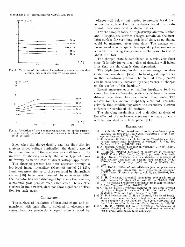
sity is uniform around tl-e circumference within 10percent. However, for pronounced nonuniformities at thecathode-insulator-vacuunm triple junction it is possibleto have larger variations in the surface-charge densities.Fig. 6 shows a graph of the charge density for variouspositionls around the insulator. Fig. 7 shows such agraph for a strongly nonuniforin case. The results arerepeatable and the nonuniformity always appears inthe same position with respect to the cathode. In mostsuch cases of nonuniform distribution, careful cleaningand polishing of the cathode was necessary to removethe nonuniform charge deposition.
178
DE TOURREIL et al.: INSULATORS FOR VACUUM APPARATUS
105 -[C m-2]
4
3
2-
.- ~~~-70 k V
60 kV
. _. *-6O50 kV
. -40kv
3 0k V
Fg6.V Iation ofIheurfceharednsiyaounanal
Fig. 6. Variation of the surface charge density around an aluminaceramic insulator stressed by dc voltages.
105c [C m-2]
4-
3-
2/ . . . 60-kV
<~~~~~~~~~.*650 kV
- .~_ . ._ *~.-40kV
*-3OkV
90 180 270-9)[ 0 1
Fig. 7. Variation of the nonuniform distribution of the surface-charge density around an alumina ceramic insulator stressedby dc voltages.
Even when the charge density was less than that fora given direct voltage application, the density aroundthe circumference of the insulator was still found to beuniform or showing exactly the same type of non-
uniformity as in the case of direct voltage application.The charging process has been observed through a
low-level image intensifier (Machlett model 25-135).Luminous areas similar to those reported by the authorsearlier [10] have been observed. In some cases, afterthe insulator has been discharged by raising the pressure,
a residual glow persists even after several hours. Theelectron beam, however, does not show significant deflec-tion for such cases.
CONCLUSIONThe surface of insulators of practical shape and di-
mensions, with ends slightly shielded in electrode re-
cesses, becomes positively charged when stressed by
90 180
179
voltages well below that needed to produce breakdownacross the surface. For the insulators tested the condi-tioned breakdown level is above 100 kV.For the samples made of high-density alumina, Teflon,
and Plexiglas, the surface charges remain on the insu-lator surface for very long periods of time, as no changecould be measured after four days. The charges canbe removed when a spark develops along the surface asa result of allowing the pressure in the vessel to rise toabout 10-2 torr.The charged state is established in a relatively short
time. It is only for voltage pulses of duration well below1 tks that the charging is time dependent.The triple junction, insulator-vacuum-negative elec-;
trode, has been shown [5]-[S] to be of great importancein the breakdown process. The field at this junctioncan be considerably increased by the presence of chargeson the surface of the insulator.
Recent measurements on similar insulators tend toshow that the surface-charge density is lower for con-ditioned insulators than for unconditioned ones. Thereasons for this are not completely clear but it is con-ceivable that conditioning alters the secondary electronemission properties of the surface.The charging mechanism and a detailed analysis of
the effect of the surface charges on the triple junctionwill be described in a later paper [11].
REFERENCES[1] I. D. Smith, "Pulse breakdown of insulator surfaces in poor
vacuum," in 1964 Proc. Int. Symp. Insulation of High Volt-ages in Vacuum, M.I.T., pp. 261.
[2] J. Shannon, S. Philp, and J. G. Trump, "Insulation of highvoltage across solid insulators in vacuum," J. Vac. Sci,Technol., vol. 2, pp. 234-239, 1965.
[3] A. Watson, "Pulsed flashover in vacuum," J. Appl. Phys.,vol. 38, pp. 2019-2023, 1967.
[41 0. Milton, "Pulsed flashover of insulators in vacuum,"IEEE Trans. Elec. Insul., vol. EI-7, pp. 9-15, Mar. 1972,
[5] M. J. Kofoid, "Phenomena at metal-dielectric junctions ofhigh voltage insulators in vacuum and magnetic field,'"AIEE Trans. (Power App. Syst.), vol. 79, pp. 991-999, Dec.1960.
[6] M. J. Kofoid, "Effect of metal-dielectric junction phenomenaon high voltage breakdown over insulators in vacuum,"AIEE Trans. (Power App. Syst.), vol. 79, pp. 999-1004, Dec.1960.
[7] P. H. Gleichauf, "Electrical breakdown over insulators inhigh vaccuum," J. Appl. Phys., vol. 22, pp. 535-541, 1951.
[8] "Electrical breakdown over insulators in high vacuum,"J. Appl. Phys., vol. 22 pp. 766-771, 1951.
[9] C. H. de Tourreil, "Surface charging of insulators stressedby high voltag2s in vacuuim," Ph.D. diss2rtation, Univ.Waterloo, Waterloo, Ont.. Canada, Apr. 1971.
[10] K. D. Srivastava and C. H. de Tourreil. "Electrical break-down across ceramic surfaces in high vacuum under dc andpulse voltages," in 1.968 Proc. 3rd Int. Symp. Discharges andElectrical Insulation in Vacuum. Paris, France. pp. 243-247.
[11] C. H. de Tourreil and K. D. Srivastava, "Mechanism ofsuirfa ce charging of high voltage insulators in vacuum,"IEEE Trans. Elec. Insul., to be published.
stei