Embed Size (px)
DESCRIPTION
physics
Citation preview

1
EXPERIMENT 5
Introduction to Diodes, Rectifiers, and Construction of a dc Power Supply
This experiment introduces diodes, transistors, and circuits that utilize these components.
While diodes are used extensively in today’s instrumentation and circuits, most stand-alone
transistors and transistor amplifiers have been replaced by integrated circuits (IC). Integrated
circuits are actually a number of transistors, resistors, and capacitive elements on a single chip.
Therefore, we will focus on diode behavior in this experiment.
Recommended reading: EDC, Sec. 7.6 and Ch. 8.
The following components will be used in this lab:
Signal diode - IN4001
Power diode - IN4004
Zener diode - IN5226
Zener diode - IN4742
Bridge rectifier - W02G
Power supply Kit
12V Transformer
I. Characteristics of Semiconductor Devices
Simple check of diode failure. Diodes have a small impedance to current flow in one
direction (forward-biased) and a large impedance in the reverse-biased mode. When diodes
fail they either short-circuit (pass current in both directions – i.e. low resistance in both
directions) or open-circuit (do not pass current at all). Since the low impedance path is the
one from anode to cathode, one needs to know which end is which. In many cases there is a
colored band painted on the package to denote the cathode end. Larger diodes often have one
end either pointed or enlarged to denote the cathode. Others simply have the diode symbol
printed on the case. Examine Appendix 1 for the electrical characteristics of the diodes to be
used in the lab.
A. A multimeter used in the resistance mode can be used to tell if a diode is operational and
reveal its polarity. (Remember: the ohmmeter acts like a battery in series with a voltmeter.)
Measure the forward and reverse “resistance” of your IN4001 signal diode using several
scales of the DVM. Are the “resistance” values measured on different scales the same? Why
not? (Hint: recall how an ohmmeter works and how different scales are obtained.)
B. Using the Two-Wire Current-Voltage Analyzer VI in the ELVIS workstation, characterize an
IN4001 signal diode in both the forward and reverse directions. Refer to experiment 1 for
instructions on using this VI. Choose the appropriate voltage ranges to give you an accurate
characterization of the diode. What is the turn on voltage of the diode? Is it what you
expected? Is there current flowing when the diode is off? Why or why not? Put a resistor in
series with the diode and hook this circuit across the Current-Hi and Current-Lo inputs to
analyze the circuit. Choose the resistor such that using the maximum voltage range possible,
the maximum current reached is ~6.5 mA. (Hint: Is any voltage dropped across the diode?)
Keep this resistor for use later in this experiment. What are the maximum voltage ranges and
maximum current ranges that can be achieved because of ELVIS? Repeat these

2
measurements with the diode reverse bias. Is the maximum voltage range the same in the
forward and reverse bias directions? Did the IV plot change with the addition of the resistor?
If so what is the role of the resistor? You should be able to explain each section of the IV
curve.
II. Transformers
Power transformers are used to alter the voltage, impedance, and current of a system without
altering the power. The type of transformer used in this lab is a 2 coil transformer wrapped
around a core that will step the voltage down from 120 Vrms to 24 V0-p from end to end or 12
V0-p from the center tap. The transformer as it comes does not have a plug to go into the wall,
so you will have to attach a plug to the transformer. It is extremely important that you
exercise caution and DO NOT PLUG IN the transformer until it has been checked by your
TA.
Transformer Preparation:
A. Carefully split the two wires on the line cord using the wire cutters as shown below.
B. Pull the wire ends apart as shown below.

3
C. Strip ½” of insulation back on each lead as shown below.
D. Twist the line cord wires with the red transformer leads as shown below.
E. Screw on the wire nuts as shown below.
4
III. Diodes used as part of power supplies.
Diodes are often used to produce dc voltages from ac voltage sources or to regulate a dc
power supply (maintaining the desired voltage from a higher voltage source). For the
remainder of this section use power diodes in your circuits.
A. Half-wave rectifier. Use the oscilloscope probe (10x) to measure the waveform of the
transformer, try both center tap and across the whole transformer. Record the frequency and
determine Vrms. Build and test the half-wave rectifier circuit shown in Figure 1. Record the
waveform across the load resistor and diode, including the peak voltages. Be sure that you
know where 0 V is on the waveforms you observe. How closely do these match what you
expect? Explain.
What is the frequency of the “ripple voltage” across the load resistor? What is the
magnitude of the ripple factor (defined as Vrms/Vdc)? Determine Vrms and Vdc
independently to answer this question. Vrms is most easily determined with the scope set
in the ac mode.
Figure 1
Reverse the diode and repeat the measurements. Explain your observations.
Add a capacitor to the rectifier as shown in Figure 2. Measure the ac and dc voltages across
the load. Calculate the ripple factor and compare to theory.
Figure 2
B. Full-Wave Bridge Rectifiers. Using power diodes, IN4004, construct the bridge rectifier
shown in Figure 3. Measure and record the waveform across the load of each circuit. What
is the current path through the circuit for each half-cycle of the transformer oscillation?
What is the frequency of the ripple (ac) and ripple factor?
115V ac 12V0-p R L 100µF
115V ac 12V0-p R
L =1k
=1 k

5
C. Full-Wave Rectifiers with Filtering. Replace the load in the bridge rectifier circuit shown
in Figure 3 with the load shown in Figure 4. Measure the ac and dc voltages across the load
at several current settings. What is the ripple frequency and ripple factor? Compare to that
measured for a half-wave, filtered rectifier.
Figure 3
Figure 4
D. Full-wave rectifier on a chip. Full wave rectifiers can be purchased as a single chip. Test
the 103018 WO2G as a bridge rectifier. Measure the ripple factor and Vdc. You will need to
know the actual dc voltage of this supply: each transistor may vary a little. Use this circuit in
parts f and g (this is the “12V” power supply pictured in Figures 5 and 6). This power supply
may not output 12 V dc, you will need to know what its output actually is.
100
100µF
A 10k
pot
V out
100
A 10k
pot
V out
12V0-p
12V0-p

6
E. Zener diode functionality. In part 1b of this experiment you explored the functionality of an
IN4001 signal diode using the Two-Wire Current-Voltage Analyzer VI. Using the same
methodology, explore the functionality of an IN5226B zener diode in forward and reverse
bias. How do the IV plots with just the zener diode compare with those from theory? Using
the same resistor as in part IB, repeat the measurements. How do these IV plots compare to
the ones taken without the resistor and to the IV plots taken with the signal diode? How
much voltage is dropped across the zener diode in forward and reverse bias? (Hint: AFTER a
diode is turned on it is just like a wire.) Is reverse or forward bias better? Why or Why not?
F. Zener diode regulator. Zener diodes are often used as a “shunt” to regulate the output
voltage of a power supply. Construct the Zener diode shunt-regulated full wave rectifier
shown in Figure 5 using the “12V” power supply from part d. Use an IN4742 zener diode;
(look up its specifications). Compare the behavior (Vdc, Vrms, ripple factor) for various load
currents. Using what you learned in the previous section about zener diodes, choose a resistor
value that will keep the power below the ratings of the resistor. If the resistor is getting hot
rethink the choice in resistor. Note: Be careful not to choose to high of a resistor or most of
the voltage while be dropped across the resistor. If the resistor is too low, the current will be
too high. A good starting point for this resistor might be 1 kΩ.
Figure 5
Make a table describing the characteristics, advantages and disadvantages of each of
the power supply wave-shaping circuits studied, using your experimental data. Include
ripple frequency, ripple factor and Vrms data.
100 100µF
A 10k
pot
V out
12V
Power
Supply
R
Zener
Diode

7
IV. Constructing a power supply
General Soldering Instructions
As you have learned in your soldering lab, the following steps should be followed for
each solder joint to be made:
1. Turn on soldering iron and set between 600 and 700. Allow soldering iron to warm up.
Wet sponge with water for use in cleaning the soldering iron tip.
2. Wipe the soldering iron tip on the wet sponge until the tip is clean and “bright”.
3. Place a tiny amount of solder directly on the tip.
4. Place the soldering iron tip, and the small amount of solder on it, in contact with both the
pad on the board and the component lead.
5. Add a small amount of solder to the joint until the pad has enough solder on it to cover
the hole and the lead. The solder joint should be smooth and should have a symmetrical
fillet.
The complete kit of parts for the power supply is shown in the figure below:
Power Supply Description
In this portion of the lab you will be building a dual voltage (+/-12 VDC) power supply
that can be used as a general laboratory supply. The theoretical basis for the design of this power
supply is attached as an Appendix to this document. To fully understand what is going on this
power supply refer to the data sheets for any component in the power supply. A lot of data sheets
can be found at www.national.com. The schematic for this power supply is as follows:

8
Power Supply PCB Construction
A photograph showing a completed PCB is found at the end of this document. You
should use it in determining the size, shape, and location of any components.
A. Install a 1 k, ¼ W resistor in the location marked R+. Pull the resistor body close to the
board and bend the leads out slightly in order to hold the resistor in place while soldering.
Solder both leads of this component as directed in the soldering instructions above. Clip the
leads close to the board using the wire cutters (cut only the excess lead wire, do not cut into
the solder joint).
Correct Resistor Installation. Incorrect Resistor Installation.
(Note that resistor body is not pulled onto
the PCB and the leads are not uniformly bent)
B. Install a 1 k, ¼ W resistor in the location marked R- as in #2 above.
C. Install a 0.1 F ceramic, non-polarized capacitor in the position marked .1 just below the
79XX and solder in place.
9
D. Install a 0.1 F ceramic, non-polarized capacitor in the position marked .1 just below the
78XX and solder in place.
Note: Electrolytic capacitors can explode if the polarity is reversed and power is applied.
Make certain that you do not install them backwards.
E. Install a 22 F polarized electrolytic capacitor in the top position labeled C2 and solder in
place. Make sure that the capacitor polarity is observed (i.e., the negative lead of the
capacitor is marked on the body with a “-“. The opposite lead is the positive lead and will
align with the “+” mark on the PCB.
F. Install a 22 F polarized electrolytic capacitor in the middle position labeled C2 and solder in
place.
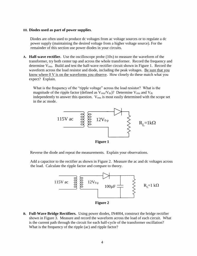
G. Install bridge rectifier DB104 into the top position labeled BR and solder in place. Make
certain that the “+” mark on the bridge rectifier lines up with the “+” mark on the PCB.
There is only one configuration where they line up correctly. The board should now look as
shown in the photo below. (Note: the bridge may not look like it fits, it does)
H. Insert a 5-position terminal block into the holes marked “- GND + GND +” (on the right
hand side in the photo above). Make sure that the holes in the terminal block that
accommodate the wires face outward as shown in the photo below.
10
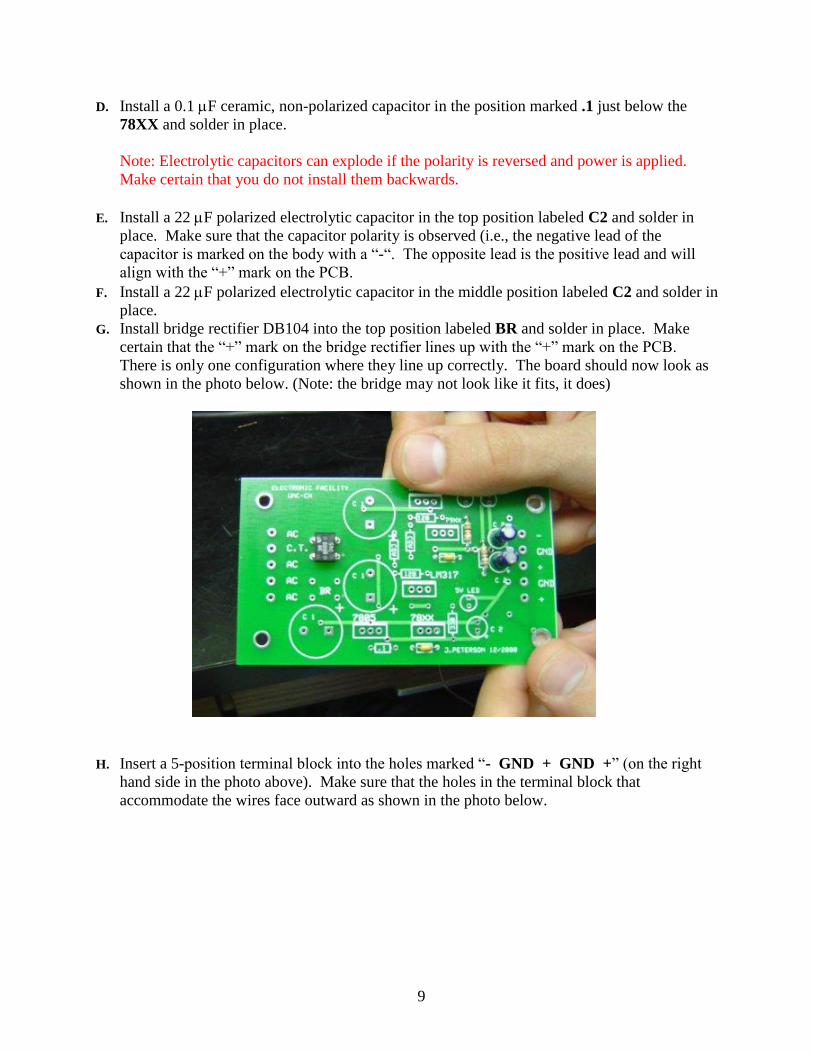
I. Insert a 5-position terminal block into the holes marked “AC C.T. AC AC AC”. Once
again, make sure that the holes in the terminal block that accommodate the wires face
outward.
J. Insert an LM7812 three-terminal regulator into the position marked 78XX. The darker, solid
line above the holes indicates that the heat sink (metallic side) of the device should line up
with the solid line.
K. Insert an LM7912 three-terminal regulator into the position marked 79XX. The darker, solid
line above the holes indicates that the heat sink (metallic side) of the device should line up
with the solid line.
L. Insert a green LED into the position marked –LED. Note that the circle around the holes is
not perfectly circular; it has a flat side. This flat indicates the negative lead of the LED. The
negative lead on the LED is the short lead and it lines up with a flat spot on the “skirt” of the
LED.
M. Insert a green LED into the position marked +LED as in “L” above.
N. Install a 3300 F polarized electrolytic capacitor in the top position labeled C1 and solder in
place. Make sure that the capacitor polarity is observed (i.e., the negative lead of the
capacitor is marked on the body with a “-“. The opposite lead is the positive lead and will
align with the “+” mark on the PCB.
O. Install a 3300 F polarized electrolytic capacitor in the middle position labeled C1 and solder
in place as in “N” above.
P. Attach an aluminum ¼” long stand-off into the four corner holes of the board using the nuts
provided.
Q. Connect the transformer to the PCB as shown in the photo below.
a. Connect one blue lead to the input terminal block top position marked AC.
b. Connect the yellow lead to the input terminal block position marked C.T.
c. Connect the remaining blue lead to the input terminal block marked AC (the one
located just below the one marked C.T.).

11
PCB Inspection
The completed PCB should be inspected for poor solder joints, solder bridges, stray
wires, or other anomalies. The completed board will look like the one in the photo below.
Power Supply Testing
NOTE: Read this section entirely before proceeding so that you will know exactly what to do
ahead of time!
12
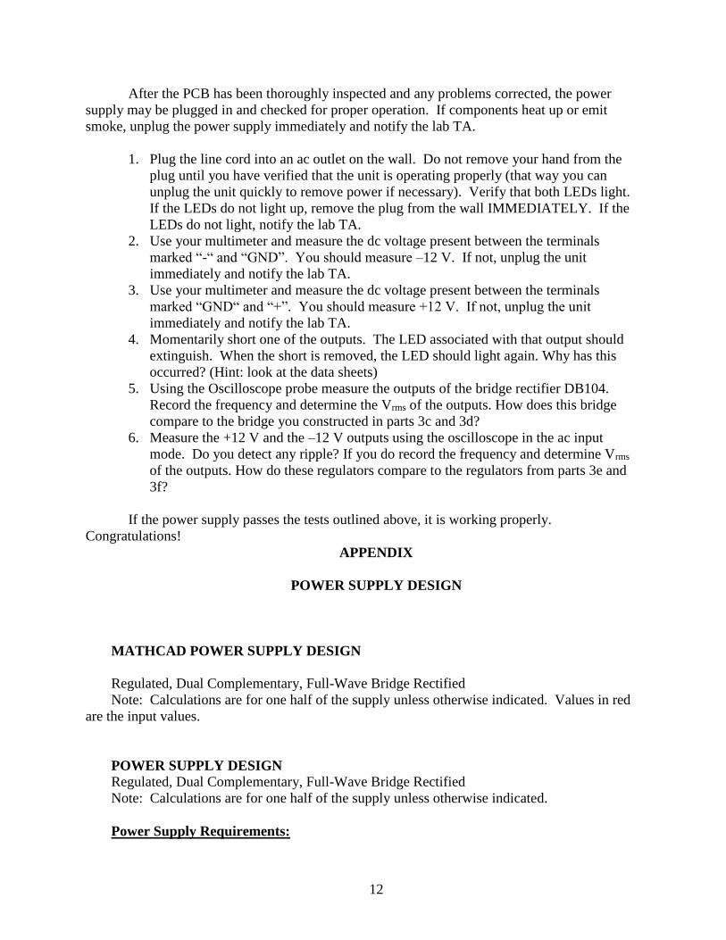
After the PCB has been thoroughly inspected and any problems corrected, the power
supply may be plugged in and checked for proper operation. If components heat up or emit
smoke, unplug the power supply immediately and notify the lab TA.
1. Plug the line cord into an ac outlet on the wall. Do not remove your hand from the
plug until you have verified that the unit is operating properly (that way you can
unplug the unit quickly to remove power if necessary). Verify that both LEDs light.
If the LEDs do not light up, remove the plug from the wall IMMEDIATELY. If the
LEDs do not light, notify the lab TA.
2. Use your multimeter and measure the dc voltage present between the terminals
marked “-“ and “GND”. You should measure –12 V. If not, unplug the unit
immediately and notify the lab TA.
3. Use your multimeter and measure the dc voltage present between the terminals
marked “GND“ and “+”. You should measure +12 V. If not, unplug the unit
immediately and notify the lab TA.
4. Momentarily short one of the outputs. The LED associated with that output should
extinguish. When the short is removed, the LED should light again. Why has this
occurred? (Hint: look at the data sheets)
5. Using the Oscilloscope probe measure the outputs of the bridge rectifier DB104.
Record the frequency and determine the Vrms of the outputs. How does this bridge
compare to the bridge you constructed in parts 3c and 3d?
6. Measure the +12 V and the –12 V outputs using the oscilloscope in the ac input
mode. Do you detect any ripple? If you do record the frequency and determine Vrms
of the outputs. How do these regulators compare to the regulators from parts 3e and
3f?
If the power supply passes the tests outlined above, it is working properly.
Congratulations!
APPENDIX
POWER SUPPLY DESIGN
MATHCAD POWER SUPPLY DESIGN
Regulated, Dual Complementary, Full-Wave Bridge Rectified
Note: Calculations are for one half of the supply unless otherwise indicated. Values in red
are the input values.
POWER SUPPLY DESIGN Regulated, Dual Complementary, Full-Wave Bridge Rectified
Note: Calculations are for one half of the supply unless otherwise indicated.
Power Supply Requirements:

13
Desired Output Voltage (VDC)
Desired Output Current (ADC)
Nominal Input Line Voltage (VrmsAC)
Input Line Voltage Variation (+/- %)
High and Low Line Input Voltage (VrmsAC)
Line Frequency (Hz)
Line Frequency (Radians)
Minimum Voltage Drop Across Regulator for Proper Regulation (from data sheet)(VDC)
Minimum Required Input Voltage (above output) to Regulator (VDC)
Forward Voltage Drop Across Single Rectifier (VDC)
Capacitor Input Filter
Filter Capacitor Value (Farads)
Ripple Voltage Estimate on Output of Capacitor Filter (Vp-p)
Voltage Regulator
Minimum Input Voltage to Rectifier to Meet Output and Regulator Requirements at Low
Line and Maximum Output Current (Vp-p)
Vo 12V
Io 0.5A
VinNom 115V
Vvar 5%
VinLow 1 Vvar( ) VinNom
VinLow 109.25V
VinHigh 1 Vvar( ) VinNom
VinHigh 120.75V
f 60Hz
2 f
376.991Hz
Vreg 2.3V
Vregin Vo Vreg
Vregin 14.3V
Vrect .6V
C 3300 106F
VripIo
2f C
Vrip 1.263V
Vmin Vo Vreg 2 VrectVrip
2
VinNom
VinLow
Vmin 16.98V

14
Minimum Input Voltage to Rectifier to Meet Output and Regulator Requirements at Low
Line and Maximum Output Current (Vrms)
<---- This is the CT voltage output specification for the transformer at
full load. Double this to get the total output voltage specification for the transformer.
Transformer Center Tap (CT) No Load and Full Load Output Voltages (Vrms)
Note: These are either measured or may sometimes be obtained from the manufacturer.
These values are different than the "rated" voltage typically found on the label and are
associated with a specific input line rms voltage value. "Full Load" here means measured or
specified at Io.
@
Maximum Transformer CT Output Voltage at High Line Input and No Load (Vrms)
Transformer CT Output Voltage at High Line Input and Full Load (Vrms)
Bridge Rectifier Output Voltage at High Line Input and Full Load (VDC)
Power Dissipated in Regulator -- High Line, Full Load (W)
<--- Check regulator data sheet to see if you need to put a heatsink
on the regulator at this dissipation level.
Vac Vmin1
2
Vac 12.007V
Vnoload 13V
Vfulload 12.13V
Vline 115V
Vtmax VnoloadVinHigh
Vline
Vtmax 13.65V
Vthf VfulloadVinHigh
Vline
Vthf 12.737V
Vbrthf Vthf 2 VrectVrip
2
1
2
Vbrthf 14.031V
Preghlfl Vbrthf Vo( ) Io
Preghlfl 1.016W

15
Maximum Current in Rectifier Diodes -- Due to charging current in capacitor and load
current (ADC)
During conduction:
by substitution:
Where i is of the form:
and where
and
Adapted from Millman and Halkias, Integrated Electronics, pg.113
So, using data from above:
(p-p Volts)
<--- Peak current in diodes for one half of the supply. Double this for
the complete supply. Note that this is a peak current requirement, not constant.
iVo
Rl
CdVo
dt
IloadVm
Rl
RlVm
Iload
iVm
Rl
sin t C Vm cos t
i Iload( ) sin t C Vm cos t
i Im sin t
Im Io2
Vm2
2C
2
arctan C Rl
Vm VfulloadVinHigh
VinNom
Vm 12.737V
Im Io2
Vm2
2 C
2 *
Im 15.853A
Vi Vmsin t