Embed Size (px)
Citation preview

© Panasonic System Networks Co., Ltd. 2010Unauthorized copying and distribution is a violationof law.
ORDER NO. KM41003051CEF13
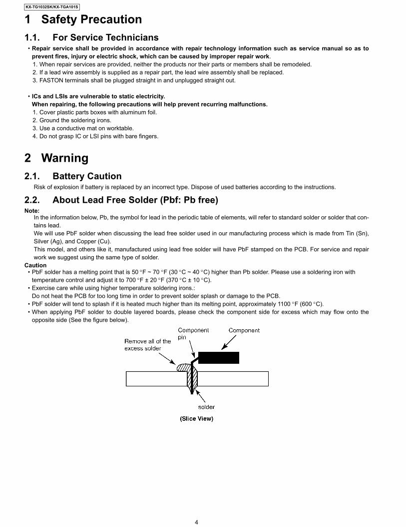
Telephone EquipmentModel No. KX-TG1032SK
KX-TGA101SExpandable Digital Cordless Answering SystemS: Silver Version(for U. S. A.)

2
KX-TG1032SK/KX-TGA101S

3
KX-TG1032SK/KX-TGA101S
TABLE OF CONTENTSPAGE PAGE
1 Safety Precaution ------------------------------------------------ 41.1. For Service Technicians --------------------------------- 4
2 Warning -------------------------------------------------------------- 42.1. Battery Caution--------------------------------------------- 42.2. About Lead Free Solder (Pbf: Pb free)--------------- 42.3. Discarding of P. C. Board-------------------------------- 5
3 Specifications ----------------------------------------------------- 64 Technical Descriptions ----------------------------------------- 7
4.1. Block Diagram (Base Unit) ------------------------------ 74.2. Circuit Operation (Base Unit) --------------------------- 84.3. Block Diagram (Handset)-------------------------------114.4. Circuit Operation (Handset)----------------------------124.5. Circuit Operation (Charger Unit) ----------------------134.6. Signal Route -----------------------------------------------14
5 Location of Controls and Components ------------------166 Installation Instructions ---------------------------------------167 Operation Instructions-----------------------------------------168 Service Mode -----------------------------------------------------17
8.1. Engineering Mode----------------------------------------178.2. Copying Phonebook Items when Repairing -------218.3. How to Clear User Setting------------------------------23
9 Troubleshooting Guide ----------------------------------------249.1. Troubleshooting Flowchart -----------------------------249.2. Troubleshooting by Symptom (Base Unit and
Charger Unit) ----------------------------------------------379.3. Troubleshooting by Symptom (Handset) -----------37
10 Disassembly and Assembly Instructions ---------------3810.1. Disassembly Instructions -------------------------------3810.2. How to Replace the Handset LCD -------------------4310.3. How and Where to fix the spacer---------------------44
11 Measurements and Adjustments---------------------------4611.1. Equipment Required-------------------------------------4611.2. The Setting Method of JIG (Base Unit) -------------4611.3. Adjustment Standard (Base Unit)---------------------4811.4. Adjustment Standard (Charger Unit)-----------------5011.5. The Setting Method of JIG (Handset) ---------------5111.6. Adjustment Standard (Handset) ----------------------5311.7. Things to Do after Replacing IC or X'tal ------------5411.8. How to Check the Handset Speaker or
Receiver ----------------------------------------------------5511.9. Frequency Table (MHz) ---------------------------------55
12 Miscellaneous ----------------------------------------------------5612.1. How to Replace the Flat Package IC----------------5612.2. How to Replace the LLP (Leadless Leadframe
Package) IC------------------------------------------------5812.3. Terminal Guide of the ICs, Transistors and
Diodes-------------------------------------------------------6013 Schematic Diagram ---------------------------------------------61
13.1. For Schematic Diagram---------------------------------6113.2. Schematic Diagram (Base Unit_Main) --------------6213.3. Schematic Diagram (Base Unit_Operation) -------6413.4. Schematic Diagram (Handset) ------------------------6613.5. Schematic Diagram (Charger Unit) ------------------68
14 Printed Circuit Board-------------------------------------------6914.1. Circuit Board (Base Unit_Main)-----------------------6914.2. Circuit Board (Base Unit_Operation) ----------------7114.3. Circuit Board (Handset) ---------------------------------7314.4. Circuit Board (Charger Unit) ---------------------------75
15 Exploded View and Replacement Parts List ----------- 7615.1. Cabinet and Electric Parts (Base Unit) ------------- 7615.2. Cabinet and Electric Parts (Handset) --------------- 7715.3. Cabinet and Electric Parts (Charger Unit) --------- 7815.4. Accessories------------------------------------------------ 7915.5. Replacement Part List ---------------------------------- 80
4
KX-TG1032SK/KX-TGA101S
1 Safety Precaution1.1. For Service Technicians
• Repair service shall be provided in accordance with repair technology information such as service manual so as toprevent fires, injury or electric shock, which can be caused by improper repair work.1. When repair services are provided, neither the products nor their parts or members shall be remodeled. 2. If a lead wire assembly is supplied as a repair part, the lead wire assembly shall be replaced. 3. FASTON terminals shall be plugged straight in and unplugged straight out.
• ICs and LSIs are vulnerable to static electricity.When repairing, the following precautions will help prevent recurring malfunctions.1. Cover plastic parts boxes with aluminum foil.2. Ground the soldering irons.3. Use a conductive mat on worktable.4. Do not grasp IC or LSI pins with bare fingers.
2 Warning2.1. Battery Caution
Risk of explosion if battery is replaced by an incorrect type. Dispose of used batteries according to the instructions.
2.2. About Lead Free Solder (Pbf: Pb free)Note:
In the information below, Pb, the symbol for lead in the periodic table of elements, will refer to standard solder or solder that con-tains lead.We will use PbF solder when discussing the lead free solder used in our manufacturing process which is made from Tin (Sn),Silver (Ag), and Copper (Cu).This model, and others like it, manufactured using lead free solder will have PbF stamped on the PCB. For service and repairwork we suggest using the same type of solder.
Caution• PbF solder has a melting point that is 50 °F ~ 70 °F (30 °C ~ 40 °C) higher than Pb solder. Please use a soldering iron with
temperature control and adjust it to 700 °F ± 20 °F (370 °C ± 10 °C). • Exercise care while using higher temperature soldering irons.:
Do not heat the PCB for too long time in order to prevent solder splash or damage to the PCB.• PbF solder will tend to splash if it is heated much higher than its melting point, approximately 1100 °F (600 °C).• When applying PbF solder to double layered boards, please check the component side for excess which may flow onto the
opposite side (See the figure below).

5
KX-TG1032SK/KX-TGA101S
2.2.1. Suggested PbF SolderThere are several types of PbF solder available commercially. While this product is manufactured using Tin, Silver, and Copper(Sn+Ag+Cu), you can also use Tin and Copper (Sn+Cu) or Tin, Zinc, and Bismuth (Sn+Zn+Bi). Please check the manufacturer’sspecific instructions for the melting points of their products and any precautions for using their product with other materials. The following lead free (PbF) solder wire sizes are recommended for service of this product: 0.3 mm, 0.6 mm and 1.0 mm.
2.3. Discarding of P. C. BoardWhen discarding P. C. Board, delete all personal information such as telephone directory and caller list or scrap P. C. Board.

6
KX-TG1032SK/KX-TGA101S
3 Specifications
Note:• Design and specifications are subject to change without notice.
Note for Service:• Operation range: Up to 300 m outdoors, Up to 50 m indoors, depending on the condition.• Analog telephone connection: Telephone Line• Optional headset: KX-TCA60, KX-TCA86, KX-TCA92,KX-TCA93, KX-TCA94
7
KX-TG1032SK/KX-TGA101S
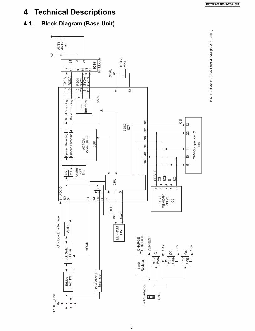
4 Technical Descriptions4.1. Block Diagram (Base Unit)
Ana
log
Fro
ntE
nd
To
TE
L_LI
NE
A B
CN
1
Brid
geR
ect D
3D
3H
ook
Sw
itch
Q3,
Q4
Aud
io
Bel
l/Cal
ler
IDIn
terf
ace
CP
U
59 54 61 52 60 56 55B
ELL
HO
OK
Off-
Hoo
k Li
ne V
olta
ge64
AD
CO
D/A
A/D
AD
PC
MC
odec
Filt
er
DS
P
Spe
ech
Dec
odin
g
Spe
ech
Enc
odin
g
BM
C
Bur
st D
ecod
ing
Bur
st E
ncod
ing
RF
Inte
rfac
e
18 19
TX
DA
RX
DA
15 2120 22
RS
SI
SY
CL
SY
DA
SY
EN
AN
T1
AN
T2
RF
Mod
ule
18 16
231
8
2114 13 12
12 13
XT
AL
X1
10.3
68M
Hz
EE
PR
OM
SC
L
SD
A
6 5
To
AC
Ada
ptor
CN
2
Lim
itR
esis
tor
CH
AR
GE
CO
NT
AC
T
VU
NR
EG
3.3V
Reg
.IC
1
2.5V
Reg
.Q
9
1.8V
Reg
.Q
83.3V
2.5V
1.8V
BB
ICIC
5
FLA
SH
ME
MO
RY
(TA
M)
TA
M C
ompa
nion
IC
RE
SE
T
CS
CS
3 4 2 1 8
SC
K
SI
SO
9
3940
3836
3762
1011
2312
IC9
IC8
IC7
IC10
KX
-TG
1032
BLO
CK
DIA
GR
AM
(B
AS
E U
NIT
)

8
KX-TG1032SK/KX-TGA101S
4.2. Circuit Operation (Base Unit)4.2.1. Outline
Base Unit consists of the following ICs as shown in Block Diagram (Base Unit) (P.7).• DECT BBIC (Base Band IC): IC7
- Handling all the audio, signal and data processing needed in a DECT base unit- Controlling the DECT specific physical layer and radio section (Burst Module Controller section)- ADPCM code filter for speech encoding and speech decoding (DSP section)- Echo-cancellation and Echo-suppression (DSP section)- Any tones (tone, sidetone, ringing tone, etc.) generation (DSP section)- DTMF receiver (DSP section)- Clock Generation for RF Module- ADC, DAC, timer, and power control circuitry- All interfaces (ex: RF module, EEPROM, LED, Analog Front End, etc.)
• RF Module: IC10- PLL Oscillator- Detector- Compress/Expander- First Mixer- Amplifier for transmission and reception
• EEPROM: IC5- Temporary operating parameters (for RF, etc.)
• FLASH MEMORY: IC9- Voice Prompt (TAM) D/L Area- ICM/OGM/MEMO Recording Area
• TAM Companion: IC8- Voice data compression and decompression- Speaker Amp- LED Driver
• Additionally,- Power Supply Circuit (+3.3 V, +2.5 V, +1.8 V output)- Crystal Circuit (10.368 MHz)- Charge Circuit- Telephone Line Interface Circuit

9
KX-TG1032SK/KX-TGA101S
4.2.2. Power Supply CircuitThe power is supplied to the DECT BBIC, RF Module, EEPROM and Charge Contact from AC Adaptor (+6.5 V) as shown inFig.101. The power supply is as follows;
• DECT BBIC (IC7): CN2 (+6.5 V) → IC1 → Q9 → IC7CN2 (+6.5 V) → IC1 → Q8 → IC7
• RF Module (IC10): CN2 (+6.5 V) → IC1 → Q9 → IC10 (PLL)CN2 (+6.5 V) → IC1 → Q10 → IC10 (Power AMP)
• EEPROM (IC5): CN2 (+6.5 V) → IC1 → Q9 → IC5
• FLASH MEMORY (IC9): CN2 (+6.5 V) → IC1 → IC9
• TAM Companion (IC8): CN2 (+6.5 V) → IC1 → Q9 → IC8CN2 (+6.5 V) → IC1 → Q8 → IC8
• Charge Contact (TP16): CN2 (+6.5 V) → R55, R56 → TP16
<Fig.101>
10
KX-TG1032SK/KX-TGA101S
4.2.3. Telephone Line Interface<Function>
• Bell signal detection• Clip signal detection• ON/OFF hook circuit
Bell & Clip (: Calling Line Identification Presentation: Caller ID) signal detection:In the standby mode, Q3 is open to cut the DC loop current and decrease the ring load.When ring voltage appears at the L1T (A) and L1R (B) leads (when the telephone rings), the AC ring voltage is transferred asfollows;
• A → C4 → R6 → R33 → IC7 Pin 60 (CID INp) • B → C3 → R4 → R35 → IC7 Pin 52 (CID INn)
ON/OFF hook circuit:In the standby mode, Q3 is open, and connected as to cut the DC loop current and to cut the voice signal. The unit is conse-quently in an on-hook condition. When IC7 detects a ring signal or press the TALK Key onto the handset, Q4 turns on and then Q3 turns on, thus providing anoff-hook condition (DC current flows through the circuit) and the following signal flow makes the loop current.
• A → D3 → Q3 → Q5 → R21 → R22 → D3 → B [OFF HOOK]
4.2.4. Transmitter/Receiver• Audio Circuits and DTMF tone signal circuits.
Base Unit and Handset mainly consist of RF Module and DECT BBIC. Base Unit and Handset transmit/receive voice signal and data signal through the antenna on carrier frequency.
Signal Path:*Refer to Signal Route (P.14).
4.2.4.1. Transmitter BlockThe voice signal input from the TEL LINE interface goes to RF Module (IC10) through DECT BBIC (IC7) as shown in Block Dia-gram (Base Unit) (P.7)The voice signal passes through the analog part of IC7 where it is amplified and converted to a digital audio stream signal. Theburst switch controller processes this stream performing encryption and scrambling, adding the various other fields to producethe GAP (Generic Access Profile) standard DECT frame, assigning to a time slot and channel etc.In IC10, the carrier frequency is changing, and frequency modulated RF signal is generated and amplified, and radiated fromantenna. Handset detects the voice signal or data signal in the circuit same as the following explanation of Receiver Block.
4.2.4.2. Receiver BlockThe signal of 1900 MHz band (1881.792 MHz ~ 1897.344 MHz) which is input from antenna is input to IC10 as shown in BlockDiagram (Base Unit) (P.7).In IC10, the signal of 1900 MHz band is downconverted to 864 kHz signal and demodulated, and goes to IC7 as GAP (GenericAccess Profile) standard DECT frames. It passes through the decoding section burst switch controller where it separates out theframe information and performs de-encryption and de-scrambling as required. It then goes to the DSP section where it is turnedback into analog audio. This is amplified by the analog front end, and goes to the TEL LINE Interface.

11
KX-TG1032SK/KX-TGA101S
4.3. Block Diagram (Handset)
CHARGECIRCUITQ4,Q5,Q9R7
CHARGECONTACTS
CHARGE(+)
CHARGE(-)
CHARGE
CHARGE DETECT
EEPROMSCL
SDA
SWITCHEDSUPPLY Q1Q1
BATTERYTERMINAL
D7
VBAT1
DC/DC-SWITCH
J1
J2
2.5VQ3
1.8VQ2
4.0V 2.5V
1.8V
LCD
RS
RESETCS
SI
SCL
CPU
AnalogFrontEnd
D/A
A/D
30
3266
67
72
62
52
45
44
58
56
59
60
6
9
10
77
ADPCMCodecFilter
DSP
SpeechDecodingSpeech
Encoding
BMC
BurstDecoding
BurstEncoding
RFInterface
RFModule
IC4
23
22
RXDA
TXDA
19
2625
24
RSSISYDASYENSYCL
16
17
XTALX1
10.368MHz
BATTERY
61
ON SWITCH
KEYPAD
ROWS
COLUMNS
1,12,40,76
27,28,34,35,36,74
BBICIC1
IC3
11
LCD-BACK LIGHT
Ringer LED
7
46
KX-TGA101 BLOCK DIAGRAM (HANDSET)
SPEAKER
RECEIVER
MIC
CN4
Headset
12345
12
KX-TG1032SK/KX-TGA101S
4.4. Circuit Operation (Handset)4.4.1. Outline
Handset consists of the following ICs as shown in Block Diagram (Handset) (P.11).• DECT BBIC (Base Band IC): IC1
- All data signals (forming/analyzing ACK or CMD signal)- All interfaces (ex: Key, Detector Circuit, Charge, DC/DC Converter, EEPROM, LCD)
• RF Module: IC4- PLL Oscillator- Detector- Compress/Expander- Amplifier for transmission and reception
• EEPROM: IC3- Temporary operating parameters (for RF, etc.)
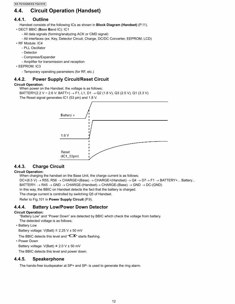
4.4.2. Power Supply Circuit/Reset CircuitCircuit Operation:
When power on the Handset, the voltage is as follows;BATTERY(2.2 V ~ 2.6 V: BATT+) → F1, L1, D1 → Q2 (1.8 V), Q3 (2.5 V), Q1 (3.3 V)The Reset signal generates IC1 (53 pin) and 1.8 V.
4.4.3. Charge CircuitCircuit Operation:
When charging the handset on the Base Unit, the charge current is as follows;DC+(6.5 V) → R55, R56 → CHARGE+(Base) → CHARGE+(Handset) → Q4 → D7→ F1 → BATTERY+... Battery... BATTERY- → R45 → GND → CHARGE-(Handset)→ CHARGE-(Base) → GND → DC-(GND)In this way, the BBIC on Handset detects the fact that the battery is charged.The charge current is controlled by switching Q5 of Handset.Refer to Fig.101 in Power Supply Circuit (P.9).
4.4.4. Battery Low/Power Down DetectorCircuit Operation:
“Battery Low” and “Power Down” are detected by BBIC which check the voltage from battery.The detected voltage is as follows;
• Battery LowBattery voltage: V(Batt) 2.25 V ± 50 mV
The BBIC detects this level and " " starts flashing.• Power Down
Battery voltage: V(Batt) 2.0 V ± 50 mVThe BBIC detects this level and power down.
4.4.5. SpeakerphoneThe hands-free loudspeaker at SP+ and SP- is used to generate the ring alarm.

13
KX-TG1032SK/KX-TGA101S
4.5. Circuit Operation (Charger Unit)4.5.1. Power Supply CircuitThe power supply is as shown.

14
KX-TG1032SK/KX-TGA101S
4.6. Signal Route

15
KX-TG1032SK/KX-TGA101S
16
KX-TG1032SK/KX-TGA101S
5 Location of Controls and ComponentsRefer to the Operating Instructions.
Note:You can download and refer to the Operating Instructions (Instruction book) on TSN Server.
6 Installation InstructionsRefer to the Operating Instructions.
Note:You can download and refer to the Operating Instructions (Instruction book) on TSN Server.
7 Operation InstructionsRefer to the Operating Instructions.
Note:You can download and refer to the Operating Instructions (Instruction book) on TSN Server.

17
KX-TG1032SK/KX-TGA101S
8 Service Mode8.1. Engineering Mode8.1.1. Base Unit

18
KX-TG1032SK/KX-TGA101S
Frequently Used Items (Base Unit)ex.)
Note:(*1) Refer to Registering a Handset (P.34)(*2) When you enter the address or New Data, please refer to the table below.
Items Address Default Data New Data RemarksFrequency 00 01 75 - - Use these items in a READ-ONLY mode to
confirm the contents. Careless rewriting maycause serious damage to the computer system.
ID 00 10~00 14 Given value - -
Desired Number (hex) Input Keys Desired Number (hex) Input Keys0 0 A [Flash] + 01 1 B [Flash] + 1. . C [Flash] + 2. . D [Flash] + 3. . E [Flash] + 49 9 F [Flash] + 5

19
KX-TG1032SK/KX-TGA101S
8.1.2. Handset

20
KX-TG1032SK/KX-TGA101S
Frequently Used Items (Handset)ex.)
Note:(*1) When you enter the address or New Data, please refer to the table below.
(*2) Use these items in a READ-ONLY mode to confirm the contents. Careless rewriting may cause serious damage to thehandset.
Items Address Default Data New Data Possible AdjustedValue MAX (hex)
Possible AdjustedValue MIN (hex)
Remarks
Battery Low 00 04 25 - - -(*2)Frequency 00 01 75 - - -
ID 00 10~00 14 Given value - - -
Desired Number (hex.) Input Keys Desired Number (hex.) Input Keys0 0 A [Flash] + 01 1 B [Flash] + 1. . C [Flash] + 2. . D [Flash] + 3. . E [Flash] + 49 9 F [Flash] + 5

21
KX-TG1032SK/KX-TGA101S
8.2. Copying Phonebook Items when RepairingYou can copy the handset phonebook to another (compatible Panasonic) handset. This will help to save the original phonebookdata which the customer has registered. Refer to the following procedures.
Note:• BS=Base Unit, HS=Handset• If the max number of handsets are already registered to the base unit, a new handset cannot be registered.• To register the handset, refer to Registering a Handset (P.34).• To cancel the handset, refer to Deregistering a handset (P.34).• To copy the handset phonebook, refer to Copying Handset Phonebook Items (P.34).

22
KX-TG1032SK/KX-TGA101S
Note:• BS=Base Unit, HS=Handset• If the max number of handsets are already registered to the base unit, a new handset cannot be registered.• To register the handset, refer to Registering a Handset (P.34).• ToTo cancel the handset, refer to Deregistering a handset (P.34).• ToTo copy the handset phonebook, refer to Copying Handset Phonebook Items (P.34).
23
KX-TG1032SK/KX-TGA101S
8.3. How to Clear User SettingUnits are reset to the Factory settings by this operation (Erase recorded Voice messages, stored Phone numbers, Caller list andetc.)
Note:• The reset menus differ depending on the following operations.• This operation should not be performed for a usual repair.
8.3.1. Resetting both base unit and handset
Note:(*1) Refer to Registering a Handset (P.34).• Handset registration will not be reset.
8.3.2. Resetting only handsetThe only handset is reset by doing the following steps to .
Note: (*2)• The registration of the base unit and the handset are cancelled.• If the handset needs to be registered to the base unit, refer to Registering a Handset (P.34).• If users do not bring the base unit with them, the registration procedure has to be done by users themselves.• Caller ID data will not be reset.
8.3.3. Delete all handset registration of base unit

24
KX-TG1032SK/KX-TGA101S
9 Troubleshooting Guide9.1. Troubleshooting Flowchart
Cross Reference:Check Power (P.25)Bell Reception (P.35)Check Battery Charge (P.26)Check Link (P.27)Check Handset Transmission (P.35)Check Handset Reception (P.35)Signal Route (P.14)Check Caller ID (P.35)Check TAM Operation (P.36)

25
KX-TG1032SK/KX-TGA101S
9.1.1. Check Power9.1.1.1. Base Unit
Is the AC Adaptor inserted into AC outlet? (*1)
Cross Reference:Power Supply Circuit (P.9)
Note:(*1) Refer to Specifications (P.6) for part number and supply voltage of AC Adaptor.
9.1.1.2. Handset
Cross Reference:Power Supply Circuit/Reset Circuit (P.12)

26
KX-TG1032SK/KX-TGA101S
9.1.2. Check Battery Charge9.1.2.1. Base Unit
Cross Reference:Charge Circuit (P.12)
9.1.2.2. Handset
Cross Reference:Check Power (P.25)Charge Circuit (P.12)
9.1.2.3. Charger Unit
Cross Reference:Charge Circuit (P.12)

27
KX-TG1032SK/KX-TGA101S
9.1.3. Check Link9.1.3.1. Base Unit
Cross Reference:Check Point (Base Unit) (P.37)Power Supply Circuit (P.9)Check the RF part (P.29)
28
KX-TG1032SK/KX-TGA101S
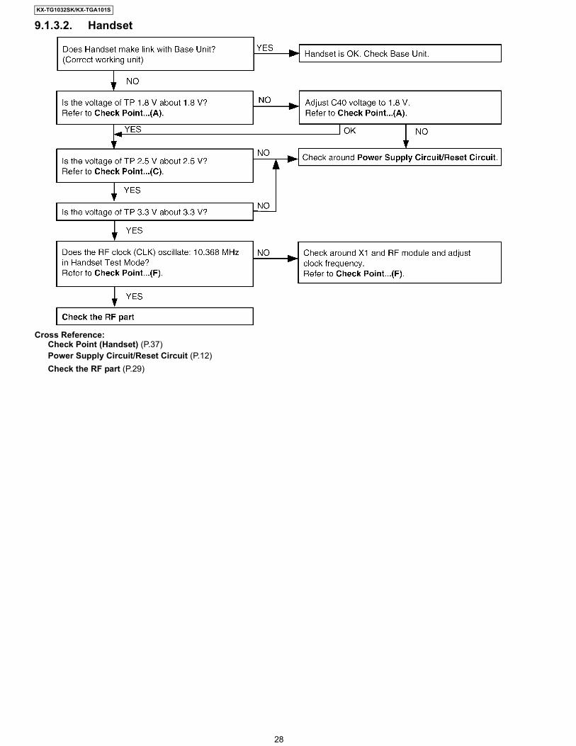
9.1.3.2. Handset
Cross Reference:Check Point (Handset) (P.37)Power Supply Circuit/Reset Circuit (P.12)Check the RF part (P.29)
29
KX-TG1032SK/KX-TGA101S
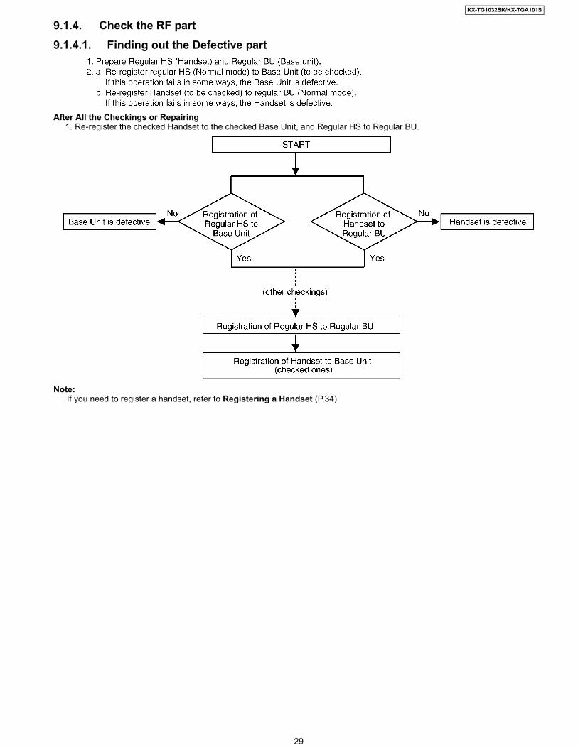
9.1.4. Check the RF part9.1.4.1. Finding out the Defective part
After All the Checkings or Repairing1. Re-register the checked Handset to the checked Base Unit, and Regular HS to Regular BU.
Note:If you need to register a handset, refer to Registering a Handset (P.34)
30
KX-TG1032SK/KX-TGA101S
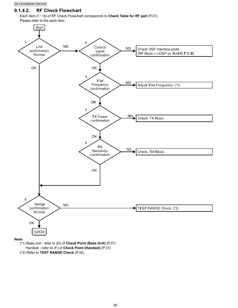
9.1.4.2. RF Check FlowchartEach item (1 ~ 6) of RF Check Flowchart corresponds to Check Table for RF part (P.31).Please refer to the each item.
Note:(*1) Base unit - refer to (D) of Check Point (Base Unit) (P.37) Handset - refer to (F) of Check Point (Handset) (P.37)(*2) Refer to TEST RANGE Check (P.32)

31
KX-TG1032SK/KX-TGA101S
9.1.4.3. Check Table for RF part
Note:(*1) Refer to Commands (P.47) for Base unit, and refer to Commands (P.52) for Handset.(*2) Refer to RF-BBIC Interface Signal Wave Form (P.33)(*3) Refer to Adjustment Standard (Base Unit) (P.48)(*4) Refer to Adjustment Standard (Handset) (P.53)(*5) Caution for measuring RSSI:It must be measured RSSI of reception unit when the timing of transmission corresponds to the timing of reception as below.EX.) RSSI waveform
No. Item BU (Base Unit) Check HS (HandSet) Check1 Link Confirmation Normal
HS, BU Mode: [Normal mode]
1. Register Regular HS to BU (to be checked).
2. Press [Talk] key of the Regular HS to establish link.
1. Register HS (to be checked) to Regular BU.
2. Press [Talk] key of the HS to establish link.
2 Control signal confirmation
HS, BU Mode: [Burst TX mode]
1. Check BBIC interface. (*2) 1. Check BBIC interface. (*2)
3 X’tal Frequency confirmation 1. Check X’tal Frequency. (*3)(10.368 MHz ± 100 Hz)
1. Check X’tal Frequency. (*4)(10.368 MHz ±100Hz)
4 TX Power confirmation (*5)
HS, BU mode Checked unit: [Burst TX mode] (*1)Regular unit: [Test RX mode] (*1)
1. Place the Regular HS about 15cm away from the BU.
2. Confirm that RSSI of the Regular HS is approximately 0.85 V by Oscilloscope. (*3)
1. Place the HS about 15cm away from the Regular BU.
2. Confirm that RSSI of the Regular BU is approximately 0.85 V by Oscilloscope. (*4)
5 RX Sensitivity confirmation (*5)
HS, BU mode Checked unit: [Test RX mode] (*1)Regular unit: [Burst TX mode] (*1)
1. Place the Regular HS about 15cm away from the BU.
2. Confirm that RSSI of the BU is approxi-mately 0.85 V by Oscilloscope. (*3)
1. Place the HS about 15cm away from the Regular BU.
2. Confirm that RSSI of the HS is approxi-mately 0.85 V by Oscilloscope. (*4)
6 Range Confirmation Normal
HS, BU Mode: [Normal mode]
1. Register Regular HS to BU (to be checked).
2. Press [Talk] key of the Regular HS to establish link.
3. Compare the range of the BU (being checked) with that of the Regular BU.
1. Register HS (to be checked) to Regular BU.
2. Press [Talk] key of the HS to establish link.3. Compare the range of the HS (being
checked) with that of the Regular HS.

32
KX-TG1032SK/KX-TGA101S
9.1.4.4. TEST RANGE CheckCircuit block which range is defective can be found by the following check.
CHART1: Setting of TX Power and RX Sensitivity in Range Confirmation TX TEST, RX TEST
Note:(*1) Refer to Commands (P.47) for Base unit, and refer to Commands (P.52) for Handset.
Item BU (Base Unit) Check HS (Handset) CheckRange Confirmation TX TEST(TX Power check)
HS, BU settingChecked unit: Low TX power (*1)Regular unit: High TX power (*1)
1. Register Regular HS to BU (to be checked).
2. Set TX Power of the BU and the Regular HS according to CHART1.
3. At distance of about 20m between HS and BU,Link OK = TX Power of the BU is OK.No Link = TX Power of the BU is NG.
1. Register HS (to be checked) to Regular BU.
2. Set TX Power of the HS and the Regular BU according to CHART1.
3. At distance of about 20m between HS and BU,Link OK = TX Power of the HS is OK.No Link = TX Power of the HS is NG.
Range Confirmation RX TEST(RX sensitivity check)
HS, BU settingChecked unit: High TX power (*1)Regular unit: Low TX power (*1)
1. Register Regular HS to BU (to be checked).
2. Set TX Power of the BU and the Regular HS according to CHART1.
3. At distance of about 20m between HS and BU,Link OK= RX Sensitivity of the BU is OK.No Link = RX Sensitivity of the BU is NG.
1. Register HS (to be checked) to Regular BU.
2. Set TX Power of the Checking HS and the Reg-ular BU according to CHART1.
3. At distance of about 20m between HS and BU,Link OK= RX Sensitivity of the HS is OK.No Link = RX Sensitivity of the HS is NG
BU (to be checked) Regular_HSTX Power TX Power
BU (Base Unit) TX Power Check Low HighBU (Base Unit) RX Sensitivity Check High Low
HS (to be checked) Regular_BUTX Power TX Power
HS (Handset) TX Power Check Low HighHS (Handset) RX Sensitivity Check High Low
33
KX-TG1032SK/KX-TGA101S
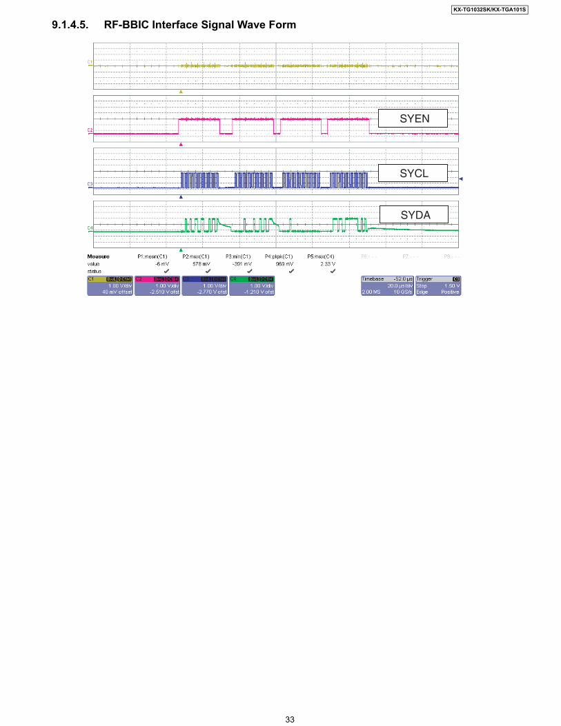
9.1.4.5. RF-BBIC Interface Signal Wave Form
SYCL
SYEN
SYDA
34
KX-TG1032SK/KX-TGA101S
9.1.5. Registering a Handset
9.1.5.1. Deregistering a handset
9.1.6. Copying Handset Phonebook ItemsYou can copy one or all of the phonebook items from one handset to another.

35
KX-TG1032SK/KX-TGA101S
9.1.7. Check Handset Transmission
Cross Reference:Signal Route (P.14)
9.1.8. Check Handset Reception
Cross Reference:How to Check the Handset Speaker or Receiver (P.55).Signal Route (P.14)
9.1.9. Check Caller ID
Cross Reference:Signal Route (P.14)
9.1.10. Bell Reception9.1.10.1. Base Unit
9.1.10.2. Handset
Cross Reference:Telephone Line Interface (P.10)Check Link (P.27)How to Check the Handset Speaker or Receiver (P.55)

36
KX-TG1032SK/KX-TGA101S
9.1.11. Check TAM Operation
A) How to change the Auto Disconnect activation (time)Some Telephone Company lines (fiber or cable) ON Hook and OFF Hook voltages are lower than conventional lines, which maycause a malfunction of Auto Disconnect detection. To solve this problem, try changing the Auto Disconnect activation throughthe procedures below.
Note:*1 Auto Disconnect doesn't detect for the first 2 seconds.*2 If the “Disable” is selected, even if the parallel-connected telephone is OFF HOOK, the line isn’t disconnected.
B) How to change the VOX levelIt makes easier to detect a small voice (caller) by raising the sensitivity of VOX level. Therefore, the recording of TAM is notturned off during a detection.
Cross Reference:Power Supply Circuit (P.9)
Auto Disconnect detect PROCEDURE at Stand-by modeEnable*1 [default] “STOP” + "ANSWER" + "SKIP" simultaneouslyDisable*2 “STOP” + "ANSWER" + "REPEAT" simultaneously
VOX Level sensitivity PROCEDURENormal [default] “STOP” + “LOCATOR" + "REPEAT” simultaneously6 dB Up “STOP” + “LOCATOR" + "SKIP” simultaneously

37
KX-TG1032SK/KX-TGA101S
9.2. Troubleshooting by Symptom (Base Unit and Charger Unit)9.2.1. Check Point (Base Unit)
Please follow the items below when BBIC or EEPROM or FLASH is replaced.Note:
After the measuring, suck up the solder of TP.*: The Setting Method of JIG (Base Unit) (P.46) is required beforehand.The connections of simulator equipment are as shown in Adjustment Standard (Base Unit) (P.48).
9.3. Troubleshooting by Symptom (Handset)9.3.1. Check Point (Handset)
Please follow the items below when BBIC or EEPROM or FLASH is replaced.Note:
After the measuring, suck up the solder of TP.*: The Setting Method of JIG (Base Unit) (P.46) is required beforehand.The connections of adjustment equipment are as shown in Adjustment Standard (Handset) (P.53).
Items Check Point
Procedure Check or Replace Parts
(A) 3.3 V Supply Confirma-tion
VDD3 1. Confirm that the voltage between test point VDD3 and GND is 3.3 V ± 0.2 V. IC1, C30, C32, R38, R39, C36,
C37(B) 2.5 V Supply Confirma-
tionVDD2 1. Confirm that the voltage between test point VDD2 and GND is 2.5 V ± 0.2 V. Q9, C70, C71
(C) 1.8 V Supply Confirma-tion
VDD1 1. Confirm that the voltage between test point VDD1 and GND is 1.8 V ± 0.1 V. Q8, R72, D12, C68
(D)* BBIC Clock Adjustment CLK 1. Input Command “rdeeprom 00 01 01”, then you can confirm the current value.2. Adjust the frequency of CLK executing the command “setfreq xx (where xx is
the value)” so that the reading of the frequency counter is 10.368000 MHz ±10 Hz.
IC10, C111, C112, X1, R73,
C62, C63
Items Check Point
Procedure Check or Replace Parts
(A)* 1.8 V Supply Adjustment 1.8 V 1. Confirm that the voltage between test point 1.8 V and GND is 1.8 V ± 0.02 V.2. Execute the command “bandgap”, then check the current value.3. Adjust the 1.8V voltage of VDD1 executing command “bandgap XX“(XX is the
value).
IC1, Q2, C10
(B) DC/DC Supply Confir-mation
3.3 V 1. Confirm that the voltage between test point 3.3 V and GND is 3.3 V ± 0.3 V(Backlight is ON).
IC1, F1, C1, C2, C3, R1, Q1, D1, L1
(C) 2.5 V Supply Confirma-tion
2.5 V 1. Confirm that the voltage between test point 2.5 V and GND is 2.5 V ± 0.1 V. IC1, Q3, C5
(D) Charge Control Check & Charge Current Monitor
Check
- 1. Apply 3.5 V between CHG(+) and CHG(-) with DC power supply and set cur-rent limit to 250 mA.
2. Confirm that the current limit LED of DC power supply is ON/OFF.3. Decrease current limit of DC power supply to 100mA.4. Confirm that the current limit LED of DC power supply is stable. (Current limiter
is ON.)(If charge control cannot be confirmed by this procedure, please use battery to hand-set power supply and try again.)
IC1, Q4, Q5, Q9, D6, D7,
D8, L4, L5, R5, R6, R7, R8, F1
(E) Battery Low Confirma-tion
- 1. Apply 2.40 V between BATT(+) and BATT(-).2. Confirm that there is no flashing of Battery Icon.3. Apply 2.25 V ± 0.08 V between BATT(+) and BATT(-).4. Confirm that there is flashing of Battery Icon.
IC1, F1, C1 C3, R12
(F)* BBIC Clock Adjustment CLK 1. Apply 2.6 V between BATT(+) and BATT(-) with DC power.2. Execute the command “conttx”.3. Input Command “rdeeprom 00 01 01”, then you can confirm the current value.4. Adjust the frequency of CLK executing the command “setfreq xx (where xx is
the value)” so that the reading of the frequency counter is 10.368000 MHz ± 10Hz.
Note:CLK is displayed only for a few seconds when executing the command “conttx”after battery is inserted.
IC1, X1, C6, C7, R19, IC4, C57

38
KX-TG1032SK/KX-TGA101S
10 Disassembly and Assembly Instructions10.1. Disassembly Instructions10.1.1. Base Unit

39
KX-TG1032SK/KX-TGA101S

40
KX-TG1032SK/KX-TGA101S
10.1.2. Handset

41
KX-TG1032SK/KX-TGA101S
10.1.3. Charger Unit

42
KX-TG1032SK/KX-TGA101S

43
KX-TG1032SK/KX-TGA101S
10.2. How to Replace the Handset LCD

44
KX-TG1032SK/KX-TGA101S
10.3. How and Where to fix the spacer

45
KX-TG1032SK/KX-TGA101S

46
KX-TG1032SK/KX-TGA101S
11 Measurements and AdjustmentsThis chapter explains the measuring equipment, the JIG connection, and the PC setting method necessary for the measurement in Troubleshooting Guide (P.24)
11.1. Equipment Required• Digital multi-meter (DMM): it must be able to measure voltage and current.• Oscilloscope.• Frequency counter: It must be precise enough to measure intervals of 1 Hz (precision; ±4 ppm)
Hewlett Packard, 53131A is recommended.• DECT tester: Rohde & Schwarz, CMD 60 is recommended.
This equipment may be useful in order to precisely adjust like a mass production.
11.2. The Setting Method of JIG (Base Unit)This section explains the PC setting to use command required in Check Point (Base Unit) (P.37).
<Preparation>• Serial JIG cable: PQZZ1CD300E*• PC which runs in DOS mode• Batch file CD-ROM for setting: PQZZTG1032M
Note:*: If you have the JIG Cable for TCD500 series
(PQZZ1CD505E), change the following values ofresistance. Then you can use it as a JIG Cable for bothTCD300 and TCD500 series. (It is an upper compatible JIGCable.)
11.2.1. ConnectionsConnect the AC adaptor to CN2 (base unit).
Connect the JIG Cable GND (black).
Connect the JIG Cable RX (red) and TX (yellow).
Note:*: COM port names may vary depending on what your PC calls it.
Resistor Old value (kΩ) New value (kΩ)R2 22 3.3R3 22 3.3R4 22 4.7R7 4.7 10

47
KX-TG1032SK/KX-TGA101S
11.2.2. How to install Batch file into P.C.
Note:• “****” varies depending on the country or models.
11.2.3. CommandsSee the table below for frequently used commands.
Command name Function Examplerdeeprom Read the data of EEPROM Type “rdeeprom 00 00 FF”, and the data from address
“00 00” to “FF” is read out.readid Read ID (RFPI) Type “readid”, and the registered ID is read out.writeid Write ID (RFPI) Type “writeid 00 18 E0 0E 98”, and the ID “0018 E0 0E
98” is written.setfreq Adjust Frequency of RFIC Type “setfreq nn”.hookoff Off-hook mode on Base Type “hookoff”.hookon On-hook mode on Base Type “hookon”.getchk Read checksum Type “getchk”.wreeprom Write the data of EEPROM Type “wreeprom 01 23 45”. “01 23” is address and “45”
is data to be written.bursttx Burst TX mode Type "bursttx"testrx Test RX mode Type "testrx"tph High TX power Type "tph"tpl Low TX power Type "tpl"
48
KX-TG1032SK/KX-TGA101S
11.3. Adjustment Standard (Base Unit)When connecting the simulator equipment for checking, please refer to below.
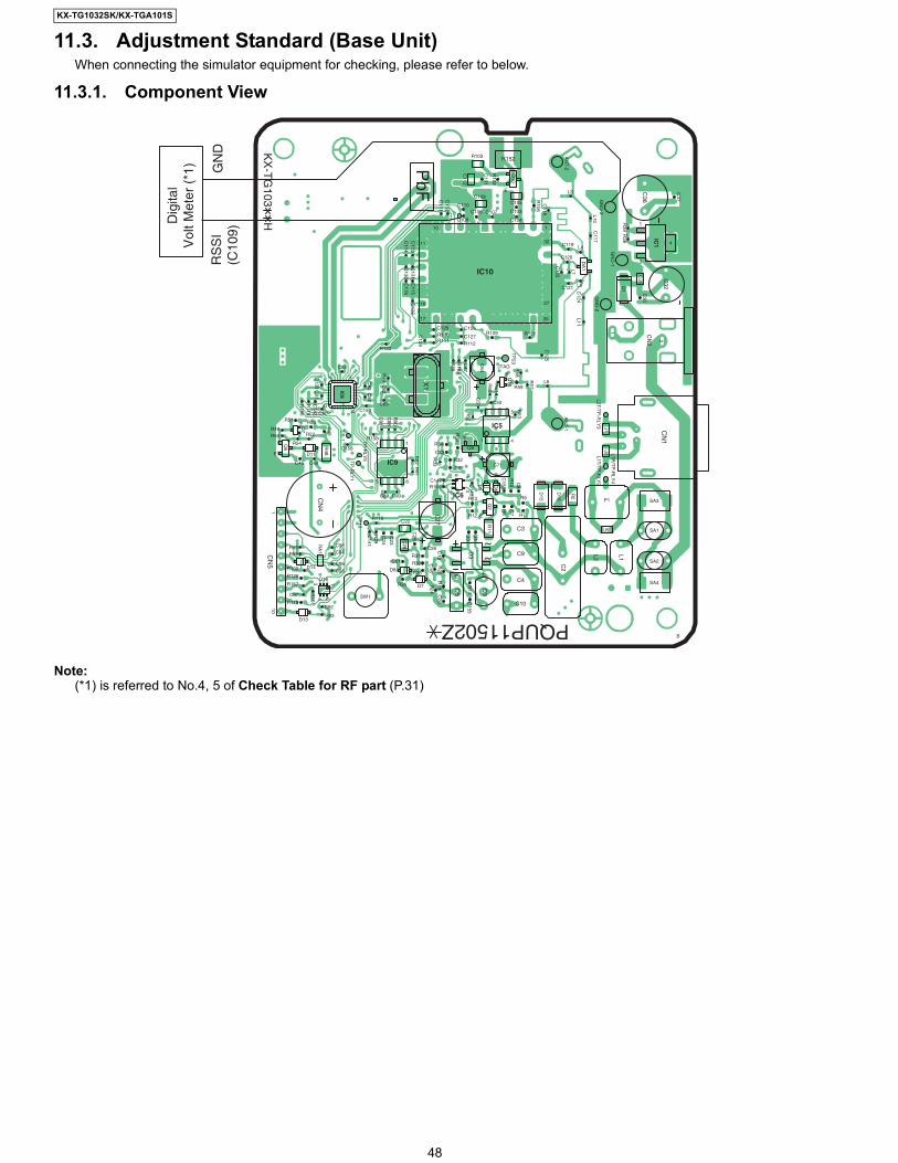
11.3.1. Component View
Note:(*1) is referred to No.4, 5 of Check Table for RF part (P.31)
C92
C97
C21
C22
C26
C53
C3
EE
C9
C4
C10
C71
C119
C120
C104
C103C107C106
C109
C110
C108C105
E
C128 C126
C127
C63C159
C85
16 9
25 32
17
24 1
1 14 4
8
8
5
5
8
C44
C158
C80
C45
C95C94
C96
C93
C147
C50
C52
C89 C90
C121
R93
R116
R50R49
R54
R99R98
R100
R120
R157
R119
R51 R53
R52
R25
R30
R31
R26
R103 R152
R109
R112R122
16
11
27
32
17
10
26
11
3
4
R110
R34R158
R32
R160
R13 R9
R7R12 E
E
E
E
E
R111R151
R59L6
JTAG
L4
L5
L3
IC10
IC5
IC6
IC9
TP
23
SA1
SA3
SA4
B
SA2
D13
Q16
SW1
D14
D11
D7
D8
P1
J5
Q9
L2T/T
P-R
LY3
L1R/T
P-R
LY4
L1T/T
P-R
LY2
AN
T-1
CN
4
CN
51
1
1
5
3
3
4
4 6
10
Q6 R48
US
-1 TP
-RLY
5TP
-RLY
1
C27
C2
C155
C20
C19
C18
C23
C24
C141
C29C
28
CN
1
C117
C125
C51
C88
C91
C82
C83
C133
C81
C46
C62
C140
C153
C8
C7
C87
C129
C64
C31
C30
C32
CN
2C
36
C37
C122
C124
C111
C112
C102
C101
C118
C113
C114
C131
C130
C115
C132
C116
R2
R57
R58
R8
R10
R118
C142
R156
R11
R163
R89
X1
Q14
R35
R14
R18
R101
R20
R29
R24
RA
1
R92
R91
R33
R61
R73
R60
R62R
90
R63
R39
AN
T-2
GN
D-3
GN
D-1DA
1
GN
D-2
R38
R106
R102
J4
J1J2
J3
L1L2
L11
1
2
L7
L10
IC8
IC1
TP
10
D3
D6
D5
D15
D16
D1
Q7
Q3
Q5
Q2
Q10
PbF
PQUP11502Z
KX
-TG
103HD
igita
lV
olt M
eter
(*1
) GN
DR
SS
I(C
109)

49
KX-TG1032SK/KX-TGA101S
11.3.2. Bottom View
Note:(A) - (D) is referred to Check Point (Base Unit) (P.37)(*1) is referred to No.3 of Check Table for RF part (P.31)
RX
TX
GN
D
L1R
L1T
DT
MF
Tes
ter
Cal
l - ID
Sim
ulat
or
BE
LLS
imul
ator
LOO
PS
imul
ator
AF
OS
C
AF
VO
LTM
ET
ER
OS
C
OS
C
600Ω
150ΩSP
U-A
RT
PC
Dig
ital
Vol
t Met
er
GN
D
LIN
E_D
C
AF
Vol
t Met
er
GN
D
BU
Z
VD
D1
VD
D3
Dig
ital
Vol
t Met
er
VD
D2
AF
VO
LTM
ET
ER D
umm
yH
ands
et
AF
OS
CM
IC
6.3 V 47uF
DC
PO
WE
R6.
0 V
Con
nect
A_1
to G
ND
.D
C_I
N
Fre
quen
cyC
ount
er (
*1)
GN
D
GN
D
CLK
(D)
(D)
(A)
(B)
(C)
Dig
ital
Vol
t Met
er
CH
AR
GE
+
CH
AR
GE
-
PQUP11502Z
KX
-TG
103
H
RE
DS
PE
AK
ER
PbF
GN
DT
XR
XD
C
J104
J102
J103
J101
BLA
CK
CH
AR
GE
2.5V
3.3V
1.8V
LIN
E-D
C
RED
BLACK
A
C84
C162
US-2
C56 C152
C74
C79
C78
C77
C72
C70
C69
C161
C68
C11
C57
C12
C58 C54
C55
C67
E
E
R115R114
R80
R79
R78
R77
R162 R56R76
R5
R6
R4
R3
R70
R69
R16
R36R72
R15R17
R21 R22
R19
R23
R75
R81
R86R85
R84
11
161732
33
4849 64
5
34
L9
IC7
IC4
D9
D17
Q8
Q4C
48
C17
C76 B
UZ
C15
C14
C13
C16
C25
C49
C14
9C
151
C47
C14
3C
134C
148
C15
0
C86
C15
4
C75
C14
4
C13
9
C13
8
C65
C61
C73
C13
6C
137
C6
L1T
L2T
DC
M
VD
D1
VD
D2
A-1
CLK
SP
+
SP
-
A-2
VD
D3
AN
T
L2R
L1R
1
1
3
2
2
4
C5
C60
C59
C66
C1
R55
R27
R28
R74
R16
1
R1
R88
R87R
68R
117
R66
R71
R15
3
R67
R83
R82
Q17
EE
E
R65
TP
15T
P16
TP
9
D12
D4
D2
Q11
Q1

50
KX-TG1032SK/KX-TGA101S
11.4. Adjustment Standard (Charger Unit)When connecting the simulator equipment for checking, please refer to below.
11.4.1. Bottom View
PQLV30053Z
TP4
TP3
1
2
A
PQUP11516Z
PbF
GND (TP4) TP3
DC POWER6.5 V
DigitalVolt
Meter
12 /2 W
GND
51
KX-TG1032SK/KX-TGA101S
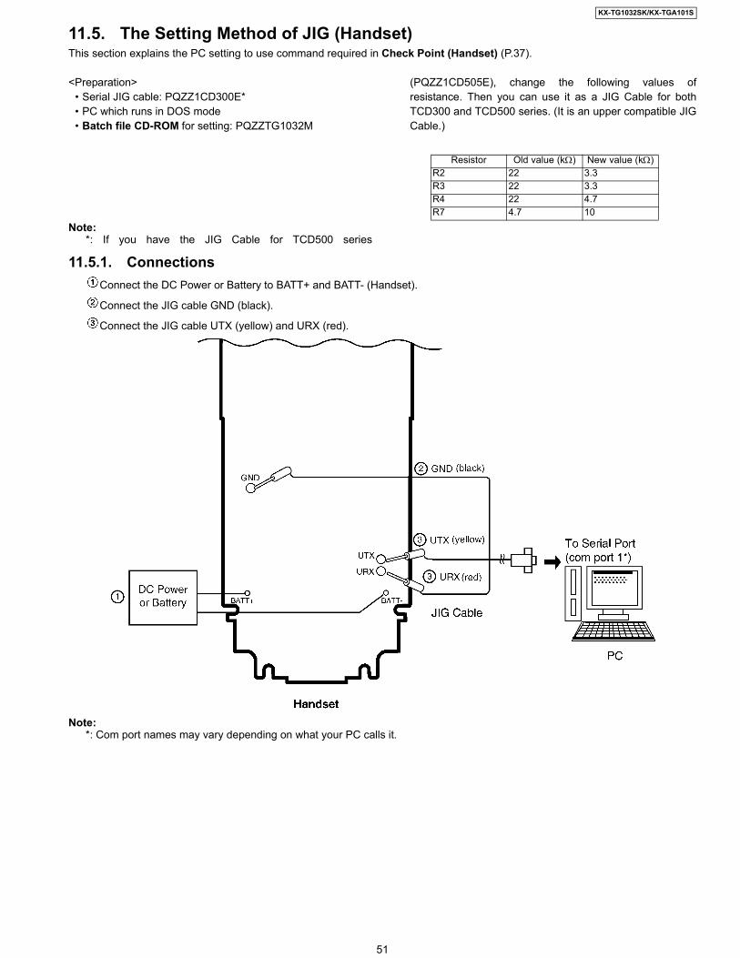
11.5. The Setting Method of JIG (Handset)This section explains the PC setting to use command required in Check Point (Handset) (P.37).
<Preparation>• Serial JIG cable: PQZZ1CD300E*• PC which runs in DOS mode• Batch file CD-ROM for setting: PQZZTG1032M
Note:*: If you have the JIG Cable for TCD500 series
(PQZZ1CD505E), change the following values ofresistance. Then you can use it as a JIG Cable for bothTCD300 and TCD500 series. (It is an upper compatible JIGCable.)
11.5.1. ConnectionsConnect the DC Power or Battery to BATT+ and BATT- (Handset).
Connect the JIG cable GND (black).
Connect the JIG cable UTX (yellow) and URX (red).
Note:*: Com port names may vary depending on what your PC calls it.
Resistor Old value (kΩ) New value (kΩ)R2 22 3.3R3 22 3.3R4 22 4.7R7 4.7 10

52
KX-TG1032SK/KX-TGA101S
11.5.2. How to install Batch file into P.C.
Note:• “*****” varies depending on the country or models.
11.5.3. CommandsSee the table below for frequently used commands.
Command name Function Examplerdeeprom Read the data of EEPROM Type “rdeeprom 00 00 FF”, and the data from address
“00 00” to “FF” is read out.readid Read ID (RFPI) Type “readid”, and the registered ID is read out.writeid Write ID (RFPI) Type “writeid 00 18 E0 0E 98”, and the ID “0018 E0 0E
98” is written.setfreq Adjust Frequency of RFIC Type “setfreq nn”.getchk Read checksum Type “getchk”.wreeprom Write the data of EEPROM Type “wreeprom 01 23 45”. “01 23” is address and “45”
is data to be written.bursttx Burst TX mode Type "bursttx"testrx Test RX mode Type "testrx"tph High TX power Type "tph"tpl Low TX power Type "tpl"

53
KX-TG1032SK/KX-TGA101S
11.6. Adjustment Standard (Handset)When connecting the simulator equipment for checking, please refer to below.
11.6.1. Component View
Note:(A) - (F) is referred to Check Point (Handset) (P.37)(*1) is referred to No.3 of Check Table for RF part (P.31)(*2) is referred to No.4, 5 of Check Table for RF part (P.31)
OS
C
AF
VO
LTM
ET
ER
LOO
PS
imul
ator
Dum
my
Bas
eU
nit
3.3V
6.3
V 4
7uF
AF
GE
NE
RA
TO
R
DC
6.5V
DC
PO
WE
R2.
30-2
.60V
DC
PO
WE
R2.
00-2
.25V
GN
D
Dig
ital
Vol
t Met
er (
*2)
UR
XU
TX
GN
D
PC
GN
D
GN
DC
HG
(-)
CH
G (
+)
CLK
(F)
(A)
(B)
(C)
(A)
(F)
(D)
(E)
Fre
quen
cyC
ount
er (
*1)
2.7
VZ
ener
AF
OS
C
MIC
-
MIC
+
1.8V
2.5V
RS
SI (
C58
) (At b
atte
ry lo
w)
PO
WE
R K
EY
SP+REV-
REV+
SP-
1uF
AF
VO
LTM
ET
ER
Osc
illos
cope
AB1
Cur
rent
Pro
be
Osc
illos
cope
C91
UTX
URXBATT-
C32
C92
C15
L3
L1
L75
L72
L71
L14
L6
C97
C148
C150
R12GND
BAT
R11
R33
R47
R61
R32
MIC- MIC+
CHG (-)
CHG (+)
MIC
D8
C147
C137C138
C152
C71C70C52
C53C51
C86
C128C127
CLK
1
27
2617
16
32
10
11
CLK_G
ANT_G
C57C58 C62
C61
C59
C60
C101
C3
C39C22
C26 JTAG
POWER
RA1
RECEIVER
R53R52 R143
R201R96
R43
R7
R202 3.3V
2.5V
E
1.8V
F1
BATT+
R125
Q8E
Q1
Q10
Q9
Q4
E
D1
C55
D19
RE
D
BLA
CK
RE
DB
LAC
K
D20
C50
C90
C49
C48
C42
C54
C56
C14
0 C72
C38
CN
4
C2
C1
C11
0
C10
8
C83
43
251
C82
C11
3
C35
C15
1
C15
7
C5
C18
C17
C21
C73
C33C
8 C37
C15
6
C10
C24
C19 1
2021 40
4160
6180C14
9
C20
C7
C6
C25
C14
C93
C94
C10
9
C10
7
C34
C36
C11
C12
C30 C
96
R25
R45
R5
R8
R89
R93
R90
R92
R54
R2
R1
R51
AN
T
R6
R46
R14
R42
D13 SP
EA
KE
RR
41R
40
R66
R63
R44
R19
R13
R23 R24 R15
R65
R64
R62
X1
Q5
Q2
Q3
D14
D7
IC1
IC3
IC4
PbF
PQUP11501ZTG103xSR (TGA101)

54
KX-TG1032SK/KX-TGA101S
11.7. Things to Do after Replacing IC or X'talIf repairing or replacing BBIC (FLASH type), EEPROM and X'tal, it is necessary to download the required data such asProgramming data or adjustment data, etc in memory.The set doesn't operate if it is not executed.
11.7.1. How to download the data11.7.1.1. Base Unit
First, operate the PC setting according to The Setting Method of JIG (Base Unit) (P.46). Then download the appropriate dataaccording to the following procedures.
Note:(*1) Refer to Check Point (Base Unit) (P.37)
11.7.2. HandsetFirst, operate the PC setting according to The Setting Method of JIG (Base Unit) (P.46). Then download the appropriate dataaccording to the following procedures.
Note:(*2) Refer to Check Point (Handset) (P.37)
Items Necessary AdjustmentBBIC(IC7)
Programs for Voice processing, interface for RF andEEPROM
1)Make sure to connect the JIG cable, then detach the DCPower.2) Execute the command “flw480 *********.hex“.3) Connect the DC Power.4) Press the PC Enter key once.5) After a few minutes, “Successful upgrade“ is displayed on thePC indicating downloading has finished.6) Detach the JIG cable, then disconnect the DC Power.7) Connect the DC Power.8)Connect the JIG cable again, and execute the command“getchk“, then confirm the checksum value is correct.If the downloading fails, start again from step 1)
EEPROM(IC5)
Adjustment parameter data(country version batch file, default batch file, etc.)
1. Clock adjustment: Refer to Check Point (D). (*1)
X'tal (X1) System clock
Items Necessary AdjustmentBBIC(IC1)
Programs for Voice processing, interface for RF andEEPROM
1)Make sure to connect the JIG cable, then detach the DCPower.2) Execute the command “flw480 *********.hex“.3) Connect the DC Power.4) Press the PC Enter key once.5) After a few minutes, “Successful upgrade“ is displayed on thePC indicating downloading has finished.6) Detach the JIG cable, then disconnect the DC Power.7) Connect the DC Power.8)Connect the JIG cable again, and execute the command“getchk“, then confirm the checksum value is correct.If the downloading fails, start again from step 1)
EEPROM(IC3)
Adjustment parameter data(country version batch file, default batch file, etc.)
1) Clock adjustment: Refer to Check Point (F). (*2)2) 1.8 V setting and battery low detection: Refer to Check Point (A), (B) and (C). (*2)
X'tal (X1) System clock

55
KX-TG1032SK/KX-TGA101S
11.8. How to Check the Handset Speaker or Receiver1. Prepare the digital voltmeter, and set the selector knob to ohm meter.2. Put the probes at the speaker terminals as shown below.
11.9. Frequency Table (MHz)
Note:Channel No. 2: In the Test Mode on Base Unit and Handset.
BASE UNIT HANDSETChannel No Transmit Frequency Receive Frequency Transmit Frequency Receive Frequency
0 1928.448 1928.448 1928.448 1928.448 1 1926.720 1926.720 1926.720 1926.720 2 1924.992 1924.992 1924.992 1924.992 3 1923.264 1923.264 1923.264 1923.264 4 1921.536 1921.536 1921.536 1921.536
56
KX-TG1032SK/KX-TGA101S
12 Miscellaneous12.1. How to Replace the Flat Package IC
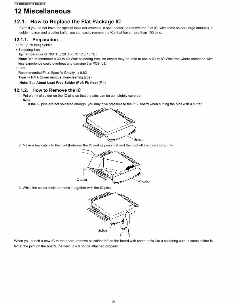
Even if you do not have the special tools (for example, a spot heater) to remove the Flat IC, with some solder (large amount), asoldering iron and a cutter knife, you can easily remove the ICs that have more than 100 pins.
12.1.1. Preparation• PbF (: Pb free) Solder• Soldering Iron
Tip Temperature of 700 °F ± 20 °F (370 °C ± 10 °C)Note: We recommend a 30 to 40 Watt soldering iron. An expert may be able to use a 60 to 80 Watt iron where someone withless experience could overheat and damage the PCB foil.
• FluxRecommended Flux: Specific Gravity → 0.82.Type → RMA (lower residue, non-cleaning type)Note: See About Lead Free Solder (Pbf: Pb free) (P.4)
12.1.2. How to Remove the IC1. Put plenty of solder on the IC pins so that the pins can be completely covered.
Note:If the IC pins are not soldered enough, you may give pressure to the P.C. board when cutting the pins with a cutter.
2. Make a few cuts into the joint (between the IC and its pins) first and then cut off the pins thoroughly.
3. While the solder melts, remove it together with the IC pins.
When you attach a new IC to the board, remove all solder left on the board with some tools like a soldering wire. If some solder isleft at the joint on the board, the new IC will not be attached properly.

57
KX-TG1032SK/KX-TGA101S
12.1.3. How to Install the IC1. Temporarily fix the FLAT PACKAGE IC, soldering the two marked pins.
*Check the accuracy of the IC setting with the corresponding soldering foil.
2. Apply flux to all pins of the FLAT PACKAGE IC.
3. Solder the pins, sliding the soldering iron in the direction of the arrow.
12.1.4. How to Remove a Solder Bridge1. Lightly resolder the bridged portion.2. Remove the remaining solder along the pins using a soldering iron as shown in the figure below.

58
KX-TG1032SK/KX-TGA101S
12.2. How to Replace the LLP (Leadless Leadframe Package) IC12.2.1. Preparation
• PbF (: Pb free) Solder• Soldering Iron
Tip Temperature of 700°F ± 20°F (370°C ± 10°C)Note:We recommend a 30 to 40 Watt soldering iron. An expert may be able to use a 60 to 80 Watt iron where someone with less experience could overheat and damage the PCB foil.
• Hot Air Desoldering ToolTemperature: 608°F ± 68°F (320°C ± 20°C)
12.2.2. Caution• To replace the IC efficiently, choose the right sized nozzle of the hot air desoldering tool that matches the IC package.• Be careful about the temperature of the hot air desoldering tool not to damage the PCB and/or IC.
12.2.3. How to Remove the IC1. Heat the IC with a hot air desoldering tool through the P. C. board.
2. Pick up the IC with tweezers, etc. when the solder is melted completely.Note:
• Be careful not to touch the peripheral parts with tweezers, etc. They are unstable.
When it is hard to melt the solder completely, heat it with a hot air desoldering tool through the IC besides through the P. C.board.
3. After removing the IC, clean the P. C. board of residual solder.
59
KX-TG1032SK/KX-TGA101S
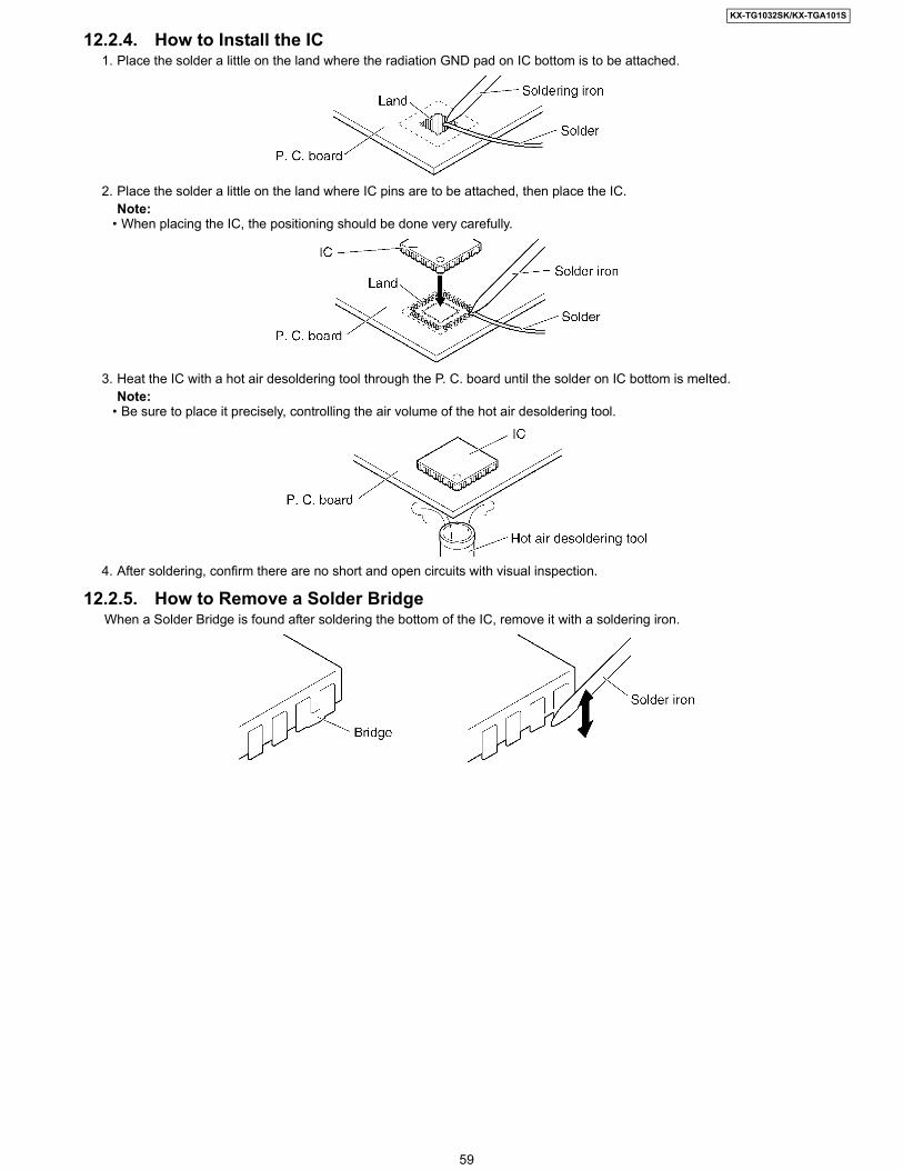
12.2.4. How to Install the IC1. Place the solder a little on the land where the radiation GND pad on IC bottom is to be attached.
2. Place the solder a little on the land where IC pins are to be attached, then place the IC.Note:
• When placing the IC, the positioning should be done very carefully.
3. Heat the IC with a hot air desoldering tool through the P. C. board until the solder on IC bottom is melted.Note:
• Be sure to place it precisely, controlling the air volume of the hot air desoldering tool.
4. After soldering, confirm there are no short and open circuits with visual inspection.
12.2.5. How to Remove a Solder BridgeWhen a Solder Bridge is found after soldering the bottom of the IC, remove it with a soldering iron.

60
KX-TG1032SK/KX-TGA101S
12.3. Terminal Guide of the ICs, Transistors and Diodes12.3.1. Base Unit
12.3.2. Handset

61
KX-TG1032SK/KX-TGA101S
13 Schematic Diagram13.1. For Schematic Diagram13.1.1. Base Unit (Schematic Diagram (Base Unit_Main))Notes:
1. DC voltage measurements are taken with voltmeter from the negative voltage line.
2. The schematic diagrams may be modified at any time with the development of new technology.
13.1.2. Handset (Schematic Diagram (Handset))Notes:
1. DC voltage measurements are taken with an oscilloscope or a tester with a ground.2. The schematic diagram may be modified at any time with the development of new technology.
13.1.3. Charger Unit (Schematic Diagram (Charger Unit))Notes:
1. DC voltage measurements are taken with voltmeter from the negative voltage line.
2. The schematic diagram may be modified at any time with the development of new technology.

62
KX-TG1032SK/KX-TGA101S
13.2. Schematic Diagram (Base Unit_Main)
L2R
J1
NC
J2
NC
L1
33u
L2
33u
K6
80
p
C9
K6
80
p
C1
0
D3
4
1
3
2
R1
1
NC
J3 NC
J4 NC
100k
R14
2.7
k
R1
5 C1
1
NC
LINE-DC
2.2k
R17
10k
R1
6
C1
3
NC
27k
R1
8
Q53
2
1
C2
0
NC
47k
R2
4
C2
1
NC
R2
5
NC
R2
6
NC
R2
NC
Q2
NC
13
2 Q41
3
2
C18
NC
K4700p
C1
4
8.2
k
R1
9 100k
R23
C2
4
NC
+2.5V
100k
R27
470k
R2
8
R1
10k
1500p
C3
1M
R4
C5
K1000p
1500p
C4
1M
R6
R5
180k
C6
K1000p
R7
NC
100k
R8
+2.5V
R9
NC
100k
R1
0
J101
J104
J103
J102
R7
61k
C7
6
NC
SW1NC
1 2
R813.3k
Q9
Q8
1
3 2
K0
.1u
C5
6
+1.8V
D1
212
15
R7
2 VDD1
+2.5V
+2.5V
NC
I/O1
O/I2
VSS3
VDD 5
CONT4
VDD2
R6
3
2.2
k
+2.5V
+2.5V
R61
1k
R6
0
22k
+3.3V
R5
8
6.8
k
NC
I/O1
O/I2
VSS3
VDD 5
CONT4
C47
NC
R54
NC
R5
2
NC
R5
1
NC
R4
8
NC
Q6
NC
13
2C4
5
NC
R49
NC
R5
3
NC
TP16
TP15
VDD3+3.3V
120
R3
8
200
R3
9
4Fin
1ADJ/GND
3Input
2Output
+8.0V
DCM
1k
R79
1k
R80
NC
R50
L2T L1T L1R
CN2
2
1
CN1
1234
5
6
2.2
k
R6
2
100k
R34
12
R2
1
D8
NC
12
D1
7
NC
12
2.2k
R59
K1
u
C7
0
100k
R32
SA
2
J220p
C52
J220p
C53
D1
NC
12
CN4
NC
12
27
R2
2
3.3M
R73
R6
5
NC
NC
R66
NC
R6
8
R69
NC
0
R70
C2
NC
R75
NCTP23
3.9
k
R5
7
R74
NC
TP10
TP9
TP-RLY1L1T/TP-RLY2L2T/TP-RLY3L1R/TP-RLY4TP-RLY5
10k
R7
7
10k
R7
8
+2.5V
C8
NC
C7
NC
D1
0p
C4
9
D1
0p
C4
8
1k
R3
5
56
R29
3.3
k
R1
17
1k
R3
3
64k1
A02
A13
A24
GND5
SDA
6SCL
7WP
8VCC
R3
180k
C1
5
NC
C1
6
NC
K2
.2u
C1
7
K1u
C22
C3
1
NC
C148 NC
R13NC
C1
2
NC
D1
0p
C1
9
R1
2
NC
1*INT1/P11
2VDDIO1
3VDD1
4VSS1
5SDA1/P25
6SCL1/P24
7*INT5/VDDE/P15
8*INT2/P12
9AVD
10AVS
11CAP
12Xtal1
13VSSRF
14RFCLKp
15RSSI/RFCLKm
16VDDRF
17
RF
CLK
d
18
TD
O
19
RD
I
20
SK
21
PD
1/S
IO
22
LE
23
P31/P
D1
24
P32/P
D2
25
P33/P
D3
26
P34/P
D4
27
TD
OD
/P35/P
D5
28
P36/P
D6
29
VS
S2
30
VD
DIO
2
31
VD
D2
32
PC
M_F
SC
/*IN
T0/P
10
33P00/UTX
34P01/URX
35P02/JTIO
36P03/SDA2
37P04/SCL2
38P05/SPICLK/PCM_CLK
39P06/SPIDO/PCM_DOUT
40P07/SPIDI/PCM_DIN
41VSS3
42VDD3
43P23/ADC1
44P17/CHARGE/INT7
45*RST
46VBAT1
47LDO1_CTRL
48LDO2_CTRL
49
LD
O1_S
ense
50
AV
S2
51
AV
D2
52
*CID
IN53
*LS
R/R
EF
54
LS
Rp/R
EF
55
RIN
GIN
G56
*MIC
/CID
OU
T57
VR
EF
m58
AG
ND
59
MIC
p60
CID
INp
61
P14/*
INT
462
P13/*
INT
363
AD
C2
64
AD
C0
2.7k
R20
K0
.1u
C2
5
L9
K0
.1u
C3
7
K0
.1u
C3
0
C4
6
NC
P1
22
SA
4
NC
21
SA
3
NC
21
BUZ
Q3
B
CE
NC
Q1B
C
E
330u
C3
6
D7
NC
AK
NC
D1
1A
K
US-1
SA
1
NC
D5
AK
NC
D6
AK
D9
AK
D1
5
NC
AK
NC
D1
6 AK
10u
C6
4
10u
C7
1
Q7
NC
BC
E
Q14B
C
E
NC
D2
AK
NC
J5
R1
53
NC
X1
132
100u
C3
2
D4
30V
AK
5.6
R56
5.6
R55
C1
NC
NC
C5
8
NC
C6
6
C134
NC
10p
C1
36
10p
C1
37
C5
0
K0
.01
u
C5
1
K0
.1u
C5
7
NC
C59
K0.1u
C60
K0.1u
C61
K0.1u
C6
5K
1u
C6
7K
0.1
u
C6
8
K1
u
C73K0.1u
C7
4K
0.1
u
C7
5 K0
.1u
C140
NC
C1
41
K0
.1u
C143
NC
C1
47
NC
C1
49
NC
C1
50
NC
C151
NC
NC
C1
52
NC
C1
53
C1
54
NC
C54
K0.022u
C4
4
NC
NC
C7
7
NC
C7
9
NC
C7
8
C72K0.22u
C6
9K
0.1
u
C1
61
NC
C62
22p
C63
8p
10p
C1
55
US-2
R36
100k
C5
5
K0
.1u
R67
NC
R160
NC
390
R116
K0
.06
8u
C2
3
R7
1N
C
RS
SI
LE
SIO
TD
OR
DI
SK
RD
Y
RE
SE
T
KE
Y0
RO
W2
KE
Y1
SPICLK
TAM_CSn
RO
W1
RO
W0
RO
W0
TAM_RSTn
RF
CL
KR
FCLK
NSA/CLIP
TAMIC_CSn
SPIDOSPIDI
Charge +
Charge -
DC_IN
GND
JTAGRX
TX
For NL
For JT
for TG1022
for TG1022
for TG1022
for TG1032/33/34
for TG1032/33/34
for TG1022
For BR
For BR
For M
IC7
IC6
IC4
IC1
IC5
EEPROM
BBIC
NC: No Components
(1)
(2)
(3)
Charge Current
RX_AF
1.8V
2.5V
3.3V
TX_AF
Loop Current
25mV p-p
0V
0.7V
Caller ID, Bell Signal
Bell signal
TX DATA
RX DATA

63
KX-TG1032SK/KX-TGA101S
C29 NC
+3.3V
C10
1
NC
R10
2
NC
R10
3
NC
Q10
NC1
32
C10
3
NC
CLK
R11
0
NC
R112
1k
C10
6
NC
+2.5V
DA
1 12
3L5 NC
ANT-2 ANT-1
R10
9
180
10k
R98
10k
R99
+2.5V +1.8V
+2.5V
+3.3V
+2.5V
10k
R89
+3.3V+3.3V
R86 NC
R85
NC
R83 NC
R84 NC
0
R88
1GP
IO4/P
CM_D
I2
GPI
O5/
PCM
_DO 9
SPI_DI
3G
PIO
6/PC
M_C
LK4
GPI
O7/
PCM
_FSC
5V
DD
16
VD
DIO
17
CLK
8*P
F
10SPI_DO
11SPI_CLK
12SPI_EN
13AVD1
14GPO9/PAOUTp
15VDDPA
16GPO8/PAOUTm
17G
PIO
0
18G
PIO
1
19V
DD
2
20V
DD
IO2
21G
PIO
2
22G
PIO
3
23*R
ST
24A
VD
2
25*LSR
26LSRp
27MICh
28*MIC
29VREFm
30VBUF
31MICp
32VREFp
33
Fin
100k
R82
R87
NC
1kR92
R90 NC
+3.3V
0
R11
4
R11
5
NC
ANT
A-1A-2
R93 NC
K1u
C10
2
C28 NC
L4 NC
CN5
82
R30
820
R31
R12
2N
C
GND-1
D13AK
D14AK
10u
C27
Q11
NC
B
C
E
GND-2
RA1
NC1
2
3
4 5
6
7
8
330
R91
C26 NC
NC
C87
NC
C88 NC
C91
C11
4
NC
C11
6
NC
C11
9
NC
C12
1
NC
C12
9
NC
C13
0
NC
C13
2
NC
C80
K0.
1u
C81
K0.
1uC
82 K0.
1u
C83
K0.
1u
C85
K0.
1u
C89 NC
C13
3
K0.
1uC14
2
K0.
1u
C86 NC
NC
C13
8N
C
C13
9
NC
C144
C11
0
K10
00p C12
7
K10
00p
NC
C15
8N
C
C15
9
C11
1
J33p
C11
2
J22p
C10
9
NC
C11
3
NC
C11
5
NC
C13
1
NC
150p
C12
6
1GND1
2ANT2
3VCCPA
4GND2
5GND3
6VCC_OC
7GND4
8RSSI
9SYRI
10GND5
11G
ND
6
12S
YE
N
13S
YD
A
14S
YC
L
15G
ND
7
16R
X_D
AT
A
17GND8
18TXDA
19GND9
20*RESET
21ANT1
22GND10
23GND11
24GND12
25GND13
26GND14
27G
ND
1528
GN
D16
29G
ND
1730
GN
D18
31A
_132
GN
D19
1uC84
R15
6
NC
GND-3
C122
NC
D10
p
C12
5
D10
p
C11
8
0
L11
2.2n
C12
0
L7
15n
C11
7
10p1n
L10
L3
C0.
5p18
0
R10
6
D10
p
C10
4
D10
p
C10
7
+2.5V +3.3V
R10
1
NC
R15
7
NC
C97
NC
Q16
1E1
2B1
3C2
4E2
5B2
6C1
10k
R10
0
270
R120
270
R119
C10
5
4.7u
C10
8
NC
2.2
R152
R111
390
2p
C12
4
C0.
5p
L6
1.5k
R151
10k
R15
8
+2.5V
Q17NC
13
2
+8.0V
R16
1
NC
R16
2
NC
C12
8
220p
SP- SP+
4.7k
R11
8
1nC92 1nC95 1nC94 1nC96 1nC93
C16
2
NC
C90
K1u
R163
NC
1SI
2SCK
3*RESET
4*CS
5*WP
6VCC
7GND
8SO
CN5-2GND
LED1CN5-7
VDDCN5-8
LED2CN5-9
KEY1CN5-10
ROW1CN5-3
ROW2CN5-4
ROW0CN5-6
KEY0CN5-5
GNDCN5-1
RESET
RD
I
TAMIC_CSnSPICLK
SPIDISPIDO
NS
A/C
LIP
SPIDO
TDO
SP(-)
SP(+)
SP
(+)
SP
(-)
AN
SW
ER
_ON
ME
SS
AG
E
RSSI
RFCLK
LESIO
SK
MESSAGE
ANSWER_ON
SPIDI
TAM_CSn
TAM_RSTn
SPICLK
KEY1
ROW1ROW2ROW0KEY0
TAM
_RST
n
RDY
RF
CLK
RF UNIT
for TG1032/33/34
Flat-cable
IC10
IC9
IC8
FLASH MEMORY
KX-TG1032 SCHEMATIC DIAGRAM (Base Unit_Main)
NC: No Components
(1)
(2)
(3)
0V
2.5V10.368MHz
RX DATA
TX DATA
3.3V

64
KX-TG1032SK/KX-TGA101S
13.3. Schematic Diagram (Base Unit_Operation)
C
LED
2A
NS
_ON 1
2
C
STOP
1 2
ERASE
1 2
LOCATOR
1 2GND
VDD
LED2T
ANS_ON
1 2
CN10-1
CN10-2
CN10-6(ROW0)
CN10-7(LED1)
CN10-8(VDD)
CN10-9(LED2)
CN10-10(KEY1)
CN10-4(ROW2)
CN10-3(ROW1)
CN10-5(KEY0)
SKIP
1 2
REPEAT
1 2
VOL_UP
1 2
VOL_DOWN
1 2
PLAY
1 2
LED1T
PLA
Y
LED
1
12
KX-TG1032 SCHEMATIC DIAGRAM (Base Unit_Operation)

65
KX-TG1032SK/KX-TGA101S
Memo

66
KX-TG1032SK/KX-TGA101S
13.4. Schematic Diagram (Handset)
1s
(When on charge)
Charge Current 3.3V
2.5V 1.8V
TX DATA
RX DATA
115kHz(Talk Mode)
0.7V
0V
25mVp-p
BATT+
BATT-
4.0V
330u
C1
47u
L1 D1
0.1
R45 1uC34
Q1
0.1R1
Q3 Q2
BATTERY +3.3V 3.3V
+2.5V +1.8V2.5V 1.8V
Q4 D7
+2.5V+1.8V
INT
12
R
12
UTX
URX
GND
+2.5V
1uC40 1uC42
+2.5V
+2.5V
POWER
1uC
39
CHG(+)
CHG(-)
BAT
CN
3R
S1
CN
3C
S2
CN
3S
I3
CN
3S
CL
4
CN
3V
DD
5
CN
3V
46
CN
3V
37
CN
3V
28
CN
3V
19
CN
3V
010
CN
3V
R11
CN
3V
OU
T12
CN
3C
AP
2-13
CN
3C
AP
2+14
CN
3C
AP
1-15
CN
3C
AP
1+16
CN
3V
SS
17
CN
3R
ES
ET
18
1uC41
68
R2
470
R510
kR
6
10k
R65
1k
R8
1k
R61
1k
R62
39k
R11
100
R13
2.2k
R25
JTAG59
LDO1_CTRL
61P
16/P
ON
/INT6
63LD
O1_
sens
e
65A
VD
2
67LS
Rp/
RE
F
69V
RE
Fm
71A
GN
D
73V
RE
Fp
4VSS1
75P
14/*
INT4
6LED2/PWM1/P21
77P
22/C
LK10
0
8LED_BIAS/P36/PD6
79A
DC
3
10SCL1/P24
12*INT2/P12
14AVS
16Xtal1
18RFCLKp
20VDDRF
22TD
O
24S
K
26LE
28P
32/P
D2
30P
AO
UTm
32P
AO
UTp
34P
33/P
D3
36TD
OD
/P35
/PD
5
38V
DD
IO2
40P
CM
_FS
C/*
INT0
/P10
42P01/URX
44P03/SDA2
46P05/SPICLK/PCM_CLK
48P07/SPIDI/PCM_DIN
50VDD3
52P17/CHARGE/INT7
54DC_STAB
56DC_CTRL
58VBAT1
60LDO2_CTRL
62P
26/S
TOP
_CH
AR
GE
64A
VS
2
66*L
SR
/RE
F
68*M
IC
70V
BU
F
72M
ICp
1*INT1/P11
3VDD1
74P
30
5LED1/PWM0/P20
76P
13/*
INT3
7LED3
78A
VS
_sen
se
9SDA1/P25
80A
DC
0
11*INT5/VDDE/P15
13AVD
15CAP
17VSSRF
19RSSI/RFCLKm
21R
FCLK
d
2VDDIO1
23R
DI
25P
D1/
SIO
27P
31/P
D1
29V
SS
PA
1
31V
DD
PA
33V
SS
PA
2
35P
34/P
D4
37V
SS
2
39V
DD
2
41P00/UTX
43P02/JTIO
45P04/SCL2
47P06/SPIDO/PCM_DOUT
49VSS3
51P23/ADC1
53*RST
55DC_I
57DC_Sense
100nC25
C94 NC
5.6k
R46
220k
R7
10k
R64
5.6k
R47
BATTERY
470
R23
3.3k
R24
LED
10 AK
Q9
120
R92
C5
2.2u
C10
2.2u
UP
12
DO
WN
12
RIG
HT
12
LEFT
12
0
12
11
22
12
3
12
41
25
12
61
2
71
28
12
TALK
12
S11 2
1kR66
C93 NC
91
2S
OFT
_C
12
SO
FT_B
12
SH
AR
P12
AS
T12
SO
FT_A
12
SP
12
CA
NC
EL
12
Q8
330RA1
1 2 3 45678
LED
1 AKLE
D2 A
KLED
3 AK
10kR14
10R
140
10R
141
10R
142
0.1u
C14
8
4.7
R12
4.7
R93
6.3V
330u
C2
5.6n
F1
820kR95
100n
C45
100n
C43
100n
C46
100n
C44
100n
C4743
0kR
94
Q5
BC
E
D8
R89 NC
R63
NC
10p
C107
C149NC
C3
K0.
1u
C36 NC
10p
C90
NC
C13
7
10p
C13
8
C19 K0.1uC24 K0.1u
C20
K0.1u
C21K0.1u
C22
K0.
1u
100n
C26
C30NC
C32
K0.1u C38
NC
C48
K0.
01u
C14
7
K0.
01u
C49
NC
C10
1
K0.
1u
C15
0
K0.
1u
C15
1K
0.1u
C91 NC
C92 NC
100p
C35
100p
C14
1
100p
C14
4
100p
C14
3
100p
C14
2
L6
3.3k
R15 NC
L14
L3
C12
10uF
C15
7N
C
1000p
C96
R19 NC
10p
C97
K0.01u
C11
X1
1 32
1uC15
56k
R12
556
kR
33
0.022
C109
C17NC
1000pC18
C6
15p
12p
C7
C8K0.22u
NC
R90
DC
_I
LDO
1_C
TRL
LDO
2_C
TRL
RESET
BELL_LED
UTXURX
JTAG
ROW
0
CO
L5C
OL4
CO
L3
CO
L2C
OL1
LESIO
SK
RD
ITD
0A
DC
3A
VS
_sen
se
STO
P_C
HA
RG
ECHARGE
DC_CTLDC_I
LDO2_CTRLLDO1_CTRL
ROW2LCD_RSLCD_SCLLCD_SI
LCD_CSB
ROW1
COL0
COL1
COL2
COL3
URX
JTAG
RSSI
COL5
RO
W0
RO
W1
RO
W3
RO
W2
COL4
DC
_CTL
RO
W3
CO
L0
UTX
LCD_
RESE
TLC
D_S
ILC
D_C
SB
LCD
_RS
LCD_
SCL
AV
S_s
ense
RFC
LK
AD
C3
LCD_BACKLIT
LCD
_BA
CK
LIT
LCD
_RE
SE
T
HE
AD
SE
T_D
ET
STO
P_C
HA
RG
E
CH
AR
GE
BE
LL_L
ED
CHARGETerminal
BA
TTE
RY
NC: No Components
IC1BBIC
(1)
(2)
(3)(4)
(5)(6)
(7)(8)
(9)
(10)(11)(12)
(13)
(14)(15)

67
KX-TG1032SK/KX-TGA101S
Sp-phone RXBeep
TX-AF
RX-AF(Handset)
TX DATA
RX DATA
10.368MHz2.5V
0V
+5V DC supply to Mic
R53 NC
R51 NC
BATTERY
+2.5V
+2.5V
CLK
C60 NC
C61 NC 1k
R52
ANT
1A0
2A1
3A2
4GND
5SDA
6SCL
7WP
8VCC
CLK_G
10u
C86
CN4
Headset Jack
1
4
2
3
5
100k
R32
D13 NC
D14 NC
MIC-
MIC+
D19
D20
R43
NC
RECEIVER
+
-
SPEAKER
+
-
Q10NC
BC
E
R96
NC
C14 NC
10p
C50
C54 NC
C55 NC
10p
C56
10p
C59
10p
C62
C70 NC
C71 NC
10p
C83
10p
C72
10p
C73
10p
C11
3
C12
7
NC
C12
8
NC
C52
K10
00p
C58
K10
00p
C10
8
NC
C82
K47
0p
100n
C156
C152
NC
C37 NC
NC
C11
0
C140
NC
150p
C53
39p
C57
1GND1
2ANT2
3VCCPA
4GND2
5GND3
6VCC_OC
7GND4
8RSSI
9SYRI
10GND5
11G
ND
6
12S
YE
N
13S
YD
A
14S
YC
L
15G
ND
7
16R
X_D
AT
A
17GND8
18TXDA
19GND9
20*RESET
21ANT1
22GND10
23GND11
24GND12
25GND13
26GND14
27G
ND
1528
GN
D16
29G
ND
1730
GN
D18
31A
_132
GN
D19
NCL75
0
R201 R202
NC
C33 NC
L71
L72
1.5k
R143
390
R54
C51
220p
10k
R40
10k
R41 R42
NC
NC
R44
MIC1
2
ANT_G
RESET
SK
LE
CHARGE
DC_CTLDC_I
LDO2_CTRLLDO1_CTRL
RD
I
SIO
RFCLK
RSSI
HEADSET_DET
TD0
KX-TGA101 SCHEMATIC DIAGRAM (Handset)
NC: No Components
IC3EEPROM
IC4RF Module
(1)
(2)
(3)(4)
(5)(6)
(7)(8)
(9)
(10)(11)(12)
(13)
(14)(15)

68
KX-TG1032SK/KX-TGA101S
13.5. Schematic Diagram (Charger Unit)
TP4
G
12 R2
TP3
12 R4
J1
2
1
10 R1
10 R3
TP1
TP2
SCHEMATIC DIAGRAM (Charger Unit)

69
KX-TG1032SK/KX-TGA101S
14 Printed Circuit Board14.1. Circuit Board (Base Unit_Main)14.1.1. Component View
KX-TG1032 CIRCUIT BOARD (Base Unit (Component View))
C92
C97
C21
C22
C26
C53
C3
EE
C9
C4
C10
C71
C11
9
C12
0
C10
4
C10
3C
107
C10
6
C10
9
C11
0
C10
8C
105
E
C12
8C
126
C12
7
C63
C15
9
C85
169
2532
17 241
11
44
8
8
5
5
8
C44
C15
8
C80
C45
C95
C94
C96
C93
C14
7
C50
C52
C89
C90
C12
1
R93
R11
6
R50
R49
R54
R99
R98
R10
0
R12
0
R15
7
R11
9
R51
R53
R52
R25
R30
R31
R26
R10
3R
152
R10
9
R11
2R
122
1611
2732
17
10
2611 3
4
R11
0
R34
R15
8
R32
R16
0
R13
R9
R7
R12
E
E
E
E
E
R11
1R
151
R59
L6
JTA
G
L4 L5
L3
IC10
IC5
IC6
IC9
TP23
SA
1
SA
3
SA
4
SA
2
D13
Q16
SW
1
D14
D11
D7
D8
P1
J5
Q9
L2T/TP-RLY3
L1R/TP-RLY4
L1T/TP-RLY2
ANT-1
CN4
CN51
1
1
5
3
3
4
4
6
10
Q6
R48
US-1
TP-RLY5
TP-RLY1
C27
C2
C155
C20C19
C18
C23
C24
C141
C29
C28
CN1
C117
C125
C51
C88
C91
C82C83
C133 C81
C46
C62
C140
C153
C8C7
C87
C129
C64
C31C30
C32
CN2C36
C37
C122
C124
C111C112
C102
C101
C118
C113C114
C131C130
C115 C132C116
R2
R57
R58
R8
R10
R118C142
R156
R11
R163R89
X1
Q14
R35
R14
R18
R101
R20
R29
R24
RA1
R92 R91
R33
R61
R73
R60
R62
R90
R63
R39
ANT-2
GND-3
GND-1
DA1
GND-2
R38
R106
R102
J4
J1 J2
J3
L1
L2
L11
1
2
L7
L10
IC8
IC1
TP10
D3
D6
D5
D15
D16
D1
Q7
Q3
Q5
Q2
Q10
PbF
PQ
UP
11502Z
KX-TG103 H B
RSSI(C109)
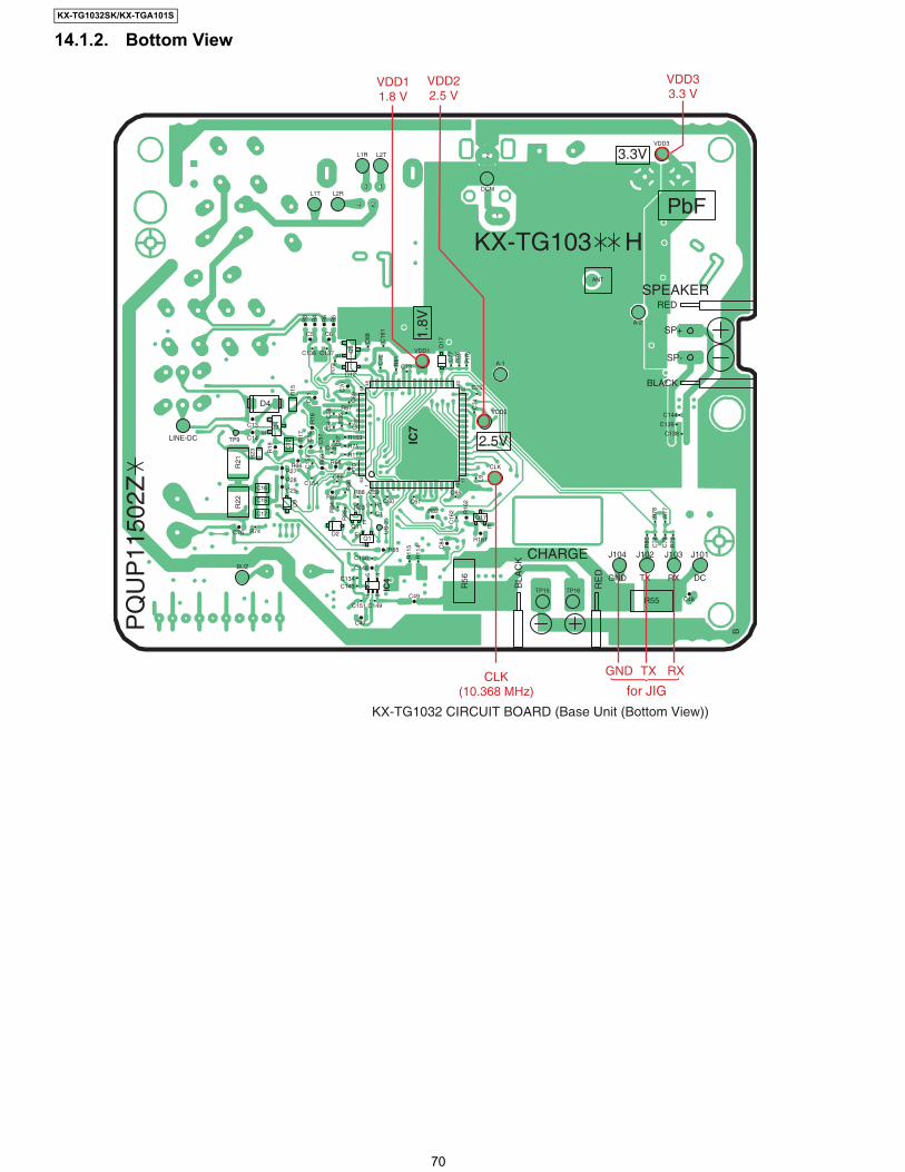
70
KX-TG1032SK/KX-TGA101S
14.1.2. Bottom View
KX-TG1032 CIRCUIT BOARD (Base Unit (Bottom View))
PQ
UP
1150
2Z
KX-TG103 H
REDSPEAKER
PbF
GND TX RX DC
J104 J102 J103 J101
BLACK
CHARGE
2.5V
3.3V
1.8V
LINE-DC
RE
D
BLA
CK
B
C84
C16
2
US
-2
C56
C15
2
C74
C79
C78
C77
C72
C70
C69
C16
1
C68
C11
C57
C12
C58
C54 C55
C67
E
E
R11
5
R11
4 R80
R79
R78
R77R
162
R56
R76
R5
R6
R4
R3
R70
R69
R16
R36
R72
R15
R17
R21
R22
R19
R23
R75
R81
R86
R85
R84
11 16
1732
334849
645
34
L9
IC7
IC4
D9
D17
Q8
Q4
C48
C17
C76
BUZ
C15
C14
C13
C16 C25
C49
C149C151
C47
C143C134
C148
C150
C86C154
C75
C144
C139
C138
C65
C61
C73
C136 C137
C6
L1T
L2T
DCM
VDD1
VDD2
A-1
CLK
SP+
SP-
A-2
VDD3
ANT
L2R
L1R
1
1
3
2
2
4
C5
C60
C59
C66
C1
R55
R27
R28
R74R161
R1
R88R87
R68R117
R66
R71
R153
R67
R83 R82Q17
EE
E
R65
TP15 TP16
TP9
D12
D4
D2Q11
Q1
VDD11.8 V
VDD22.5 V
CLK(10.368 MHz)
GND TX RX
VDD33.3 V
for JIG

71
KX-TG1032SK/KX-TGA101S
14.2. Circuit Board (Base Unit_Operation)14.2.1. Bottom View
KX-TG103 H
REPEAT
ERASE
LOCATOR
1 10
PQUP11503Z
VOL_DOWN VOL_UP
A
STOP
PLAY
CN10
SKIP ANS_ON
LED
2
LED
1
GN
D
LED
1
LED
2V
DD
PbF
KX-TG1032 CIRCUIT BOARD (Base Unit_Operation (Bottom View))

72
KX-TG1032SK/KX-TGA101S
Memo

73
KX-TG1032SK/KX-TGA101S
14.3. Circuit Board (Handset)14.3.1. Component View
C91
UTX
URXBATT-
C32
C92
C15
L3
L1
L75
L72
L71
L14
L6
C97
C148
C150
R12GND
BAT
R11
R33
R47
R61
R32
MIC-MIC+
CHG (-) CHG (+)MIC
D8
C147
C137C138
C152
C71 C70
C52C53 C51
C86
C128C127
CLK
1
27
26 17
16
32
10
11
CLK_G
ANT_G
C57
C58C62
C61
C59
C60
C101
C3
C39C22
C26JTAG
POWER
RA1
RECEIVER
R53R52R143
R201 R96
R43
R7
R2023.3V2.5V
E
1.8V
F1
BATT+
R125
Q8E
Q1
Q10
Q9
Q4
E
D1
C55
D19
RE
D
BLA
CK
RE
DB
LAC
K
D20
C50
C90
C49
C48
C42
C54
C56
C140C
72C
38
CN
4
C2
C1
C110
C108
C83
43
25 1
C82
C113
C35
C151
C157
C5
C18
C17
C21
C73
C33 C
8C37
C156
C10
C24
C191
20214041
60 61
80
C149
C20
C7
C6
C25
C14
C93
C94
C109
C107
C34
C36
C11
C12
C30C
96
R25
R45
R5
R8
R89
R93
R90
R92
R54
R2
R1
R51
AN
T
R6
R46
R14
R42
D13
SP
EA
KE
R
R41
R40 R
66 R63
R44
R19
R13
R23
R24
R15
R65
R64
R62
X1
Q5
Q2
Q3
D14
D7
IC1
IC3
IC4
PbF
PQUP11501ZTG103xSR (TGA101)
KX-TGA101 CIRCUIT BOARD (Handset (Component View))
for JIG
BATT+ BATT-
GND
UTX
URX3.3 V
2.5 V
1.8 V
CLK(10.368 MHz)
RSSI(C58)
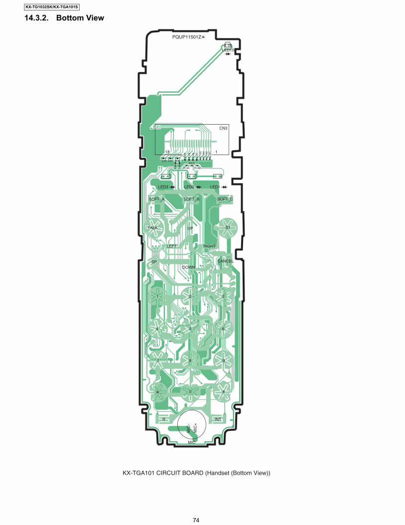
74
KX-TG1032SK/KX-TGA101S
14.3.2. Bottom View
CN3
18 1
R140
R141C40 R95
R94
C43
C44
C45
C46
C47
C14
3C
144
C14
2C
141
C41
R142
PQUP11501Z
LEFT
TALK
SP
1 2 3
4 5 6
7 8 9
INTR
C
MIC
MIC
-
MIC
+
0 #
UP
DOWN
SOFT_B SOFT_CSOFT_A
CANCEL
S1
RIGHT
LED3 LED2 LED1
LED10
KX-TGA101 CIRCUIT BOARD (Handset (Bottom View))

75
KX-TG1032SK/KX-TGA101S
14.4. Circuit Board (Charger Unit)14.4.1. Component View
14.4.2. Bottom View
PQLV30053Z
R3
R4
R1
J1
A
R2
1
2
PQUP11516Z
PbF
CIRCUIT BOARD (Charger Unit (Component View))
PQLV30053Z
TP4
TP3
1
2
A
PQUP11516Z
PbF
CIRCUIT BOARD (Charger Unit (Bottom View))

76
KX-TG1032SK/KX-TGA101S
15 Exploded View and Replacement Parts List15.1. Cabinet and Electric Parts (Base Unit)

77
KX-TG1032SK/KX-TGA101S
15.2. Cabinet and Electric Parts (Handset)
Note:(*1) This cable is fixed by welding. Refer to How to Replace the Handset LCD (P.43).(*2) The rechargeable Ni-MH battery HHR-4DPA is available through sales route of Panasonic.(*3) Attach the spacer (No. 122) to the exact location described above.

78
KX-TG1032SK/KX-TGA101S
15.3. Cabinet and Electric Parts (Charger Unit)

79
KX-TG1032SK/KX-TGA101S
15.4. Accessories
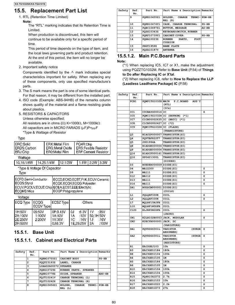
80
KX-TG1032SK/KX-TGA101S
15.5. Replacement Part List1. RTL (Retention Time Limited)
Note:The “RTL” marking indicates that its Retention Time isLimited.When production is discontinued, this item willcontinue to be available only for a specific period oftime.This period of time depends on the type of item, andthe local laws governing parts and product retention.At the end of this period, the item will no longer beavailable.
2. Important safety noticeComponents identified by the mark indicates specialcharacteristics important for safety. When replacing anyof these components, only use specified manufacture’sparts.
3. The S mark means the part is one of some identical parts.For that reason, it may be different from the installed part.
4. ISO code (Example: ABS-94HB) of the remarks columnshows quality of the material and a flame resisting gradeabout plastics.
5. RESISTORS & CAPACITORSUnless otherwise specified;All resistors are in ohms (Ω) K=1000Ω, M=1000kΩAll capacitors are in MICRO FARADS (µF)P=µµF*Type & Wattage of Resistor
15.5.1. Base Unit15.5.1.1. Cabinet and Electrical Parts
15.5.1.2. Main P.C.Board PartsNote:
(*1) When replacing IC5, IC7 or X1, make the adjustmentusing PQZZTG1032M. Refer to Base Unit (P.54) of Thingsto Do after Replacing IC or X'tal.(*2) When replacing IC8, refer to How to Replace the LLP(Leadless Leadframe Package) IC (P.58)
Safety Ref. No.
Part No. Part Name & Description Remarks
1 PQKM10755Z1 CABINET BODY PS-HB2 PQQT23193Z LABEL, CHARGE3 L0AA02A00072 SPEAKER4 PQHG10729Z RUBBER PARTS, SPEAKER5 PQHR10778Z GUIDE, SPEAKER ABS-HB6 PQJT10241V CHARGE TERMINAL (L) 7 PQJT10242X CHARGE TERMINAL (R) 8 PQKE10454Z1 HOLDER, CHARGE TERMI-
NAL (L) POM-HB
9 PQKE10455Z1 HOLDER, CHARGE TERMI-NAL (R)
POM-HB
10 PQKE10474Y1 CASE, CHARGE TERMINAL PS-HB11 PQBC10497Z1 BUTTON, MESSAGE AS-HB12 PQSX10343Z KEYBOARD SWITCH, RUBBER 13 PQKF10739Y1 CABINET COVER PS-HB14 PQHA10023Z RUBBER PARTS, FOOT
CUSHION15 PNGT1959Z NAME PLATE 16 PQSA10187Y ANTENNA
Safety Ref. No.
Part No. Part Name & Description Remarks
PCB1 PQWP1TG1032H MAIN P.C.BOARD ASS'Y(RTL)
(ICs)IC1 C0CBAYG00016 IC SIC5 PQWI1TG1032H IC (EEPROM) (*1) IC7 C1CB00002635 IC (BBIC) (*1) IC8 C1CB00002427 IC (*2) IC9 PQWI3TG1032H IC (FLASH)
(TRANSISTORS)Q3 B1ACGP000007 TRANSISTOR(SI) Q4 PQVTBF822T7 TRANSISTOR(SI) Q5 2SD1994A TRANSISTOR(SI) Q8 B1ADGE000004 TRANSISTOR(SI) Q9 B1ADGE000004 TRANSISTOR(SI) Q14 B1ADCF000161 TRANSISTOR(SI) Q16 XP0421300L TRANSISTOR(SI)
(DIODES)D3 B0EDER000009 DIODE(SI) D4 MA1Z300 DIODE(SI) SD9 MA111 DIODE(SI) SD12 MA112 DIODE(SI) SD13 MA111 DIODE(SI) SD14 MA111 DIODE(SI) SDA1 B0DDCM000001 DIODE(SI)
(COILS)L1 PQLQXF330K COIL SL2 PQLQXF330K COIL SL7 MQLRF15NJFB COIL L10 MQLRF1N0DFB COIL C120 ELJRF2N2ZFB COIL S
(JACKS)CN1 K2LB102B0053 JACK, MODULAR S CN2 K2ECYB000001 JACK, DC
(VARISTORS) SA1 PQVDDSS301L VARISTOR (SURGE
ABSORBER) S
SA2 PQVDDSS301L VARISTOR (SURGEABSORBER)
S
(RESISTORS)R1 ERJ2GEJ103 10k SR3 ERJ3GEYJ184 180k SR8 ERJ3GEYJ104 100k SR4 ERJ3GEYJ105 1M SR5 ERJ3GEYJ184 180k SR6 ERJ3GEYJ105 1M SR10 ERJ3GEYJ104 100k SR14 ERJ3GEYJ104 100k SR15 PQ4R10XJ272 2.7k SR16 ERJ3GEYJ103 10k SR17 ERJ3GEYJ222 2.2k SR18 ERJ3GEYJ273 27k S
Safety Ref. No.
Part No. Part Name & Description Remarks

81
KX-TG1032SK/KX-TGA101S
R19 ERJ3GEYJ822 8.2k SR20 ERJ3GEYJ272 2.7k SR21 ERJ12YJ120 12 R22 ERJ12YJ270 27 R23 ERJ3GEYJ104 100k SR24 ERJ3GEYJ473 47k SR27 ERJ3GEYJ104 100k SR28 ERJ3GEYJ474 470k SR29 ERJ2GEJ560X 56 SR30 ERJ3GEYJ820 82 SR31 ERJ3GEYJ821 820 SR32 ERJ3GEYJ104 100k SR33 ERJ2GEJ102 1k SR34 ERJ3GEYJ104 100k SR35 ERJ3GEYJ102 1k SR36 ERJ2GEJ104 100k SR38 ERJ2RKF1200 120 R39 ERJ2RKF2000 200 R55 ERJ1TYJ5R6U 5.6 R56 ERJ1TYJ5R6U 5.6 R57 ERJ2GEJ392 3.9k SR58 ERJ2GEJ682 6.8k SR59 ERJ3GEYJ222 2.2k SR60 ERJ2GEJ223 22k SR61 ERJ2GEJ102 1k SR62 ERJ2GEJ222 2.2k SR63 ERJ2GEJ222 2.2k SR70 ERJ3GEY0R00 0 SR71 ERJ2GEJ332 3.3k SR72 ERJ2GEJ150 15 SR73 ERJ2GEJ335 3.3M SR76 ERJ2GEJ102 1k SR77 ERJ2GEJ103 10k SR78 ERJ2GEJ103 10k SR79 ERJ2GEJ102 1k SR80 ERJ2GEJ102 1k SR81 ERJ2GEJ332 3.3k SR82 ERJ3GEYJ104 100k SR88 ERJ2GE0R00 0 SR89 ERJ2GEJ103 10k SR91 ERJ2GEJ331 330 SR92 ERJ2GEJ102 1k SR98 ERJ2GEJ103 10k SR99 ERJ2GEJ103 10k SR100 ERJ2GEJ103 10k SR106 ERJ3GEYJ181 180 SR109 ERJ3GEYJ181 180 SR111 ERJ2GEJ391 390 SR112 ERJ2GEJ102 1k SR114 ERJ2GE0R00 0 SR116 ERJ2GEJ391 390 SR117 ERJ2GEJ332 3.3k SR118 ERJ2GEJ472X 4.7k SR119 ERJ3GEYJ271 270 SR120 ERJ3GEYJ271 270 SR151 ERJ2GEJ152 1.5k SR152 ERJ12YJ2R2 2.2 R158 ERJ2GEJ103 10k SL11 ERJ2GE0R00 0 S
(CAPACITORS)C3 F1B2H152A048 1500p C4 F1B2H152A048 1500p C5 ECUV1H102KBV 0.001 C6 ECUV1H102KBV 0.001 C9 F1B2H681A070 680 C10 F1B2H681A070 680 C14 ECUV1H472KBV 0.0047 C17 PQCUV1A225KB 2.2 C19 ECUV1H100DCV 10p C22 PQCUV1A105KB 1 C23 ECUV1C683KBV 0.068 C25 ECUV1C104KBV 0.1 C27 F2G1H1000009 10
Safety Ref. No.
Part No. Part Name & Description Remarks
C30 ECUV1C104KBV 0.1 C32 ECEA1CK101 100 SC36 ECEA0JKA331 330 C37 ECUV1C104KBV 0.1 C48 ECUV1H103KBV 0.01 C50 ECUE1C103KBQ 0.01 C51 ECUE1A104KBQ 0.1 C52 ECUV1H221JCV 220p C53 ECUV1H221JCV 220p C54 ECUE1C223KBQ 0.022 C55 ECUE1A104KBQ 0.1 C56 ECUV1C104KBV 0.1 C59 ECUE1A104KBQ 0.1 C60 ECUE1A104KBQ 0.1 C61 ECUE1A104KBQ 0.1 C62 ECUE1H220JCQ 22p C63 ECUE1H8R0DCQ 8p C64 F2G1C1000014 10 C65 ECUE0J105KBQ 1 C67 ECUE1A104KBQ 0.1 C68 ECUE0J105KBQ 1 C69 ECUE1A104KBQ 0.1 C70 ECUV1A105KBV 1 C71 F2G1C1000014 10 C72 ECJ0EB0J224K 0.22 SC73 ECUE1A104KBQ 0.1 C74 ECUE1A104KBQ 0.1 C75 ECUE1A104KBQ 0.1 C80 ECUE1A104KBQ 0.1 C81 ECUE1A104KBQ 0.1 C82 ECUE1A104KBQ 0.1 C83 ECUE1A104KBQ 0.1 C84 ECUV1A105KBV 1 C85 ECUE1A104KBQ 0.1 C90 ECUE0J105KBQ 1 C92 ECUE1H102KBQ 0.001 C93 ECUE1H102KBQ 0.001 C94 ECUE1H102KBQ 0.001 C95 ECUE1H102KBQ 0.001 C96 ECUE1H102KBQ 0.001 C102 PQCUV1A105KB 1 C111 ECUE1H330JCQ 33p SC112 ECUE1H220JCQ 22p C113 ECUE1H100DCQ 10p C142 ECUE1A104KBQ 0.1 C104 ECUE1H100DCQ 10p C105 F1J0J4750005 4.7 C107 ECUE1H100DCQ 10p C110 ECUE1H102KBQ 0.001 C115 ECUE1H100DCQ 10p C117 ECUE1H100DCQ 10p C118 ECUE1H100DCQ 10p C124 ECUE1H2R0CCQ 2 C125 ECUE1H100DCQ 10p C126 ECUE1H151JCQ 150p C127 ECUE1H102KBQ 0.001 C128 ECUE1H221JCQ 220p C129 ECUE1H100DCQ 10p C131 ECUE1H100DCQ 10p C133 ECUE1A104KBQ 0.1 C136 ECUE1H100DCQ 10p C137 ECUE1H100DCQ 10p C141 ECUE1A104KBQ 0.1 C155 ECUV1H100DCV 10p L3 ECJ0EC1H0R5C 0.5 SL6 ECJ0EC1H0R5C 0.5 S
(OTHERS)CN5 WBX10SH-5GG PARALLEL WIRE IC10 PQLP10291Z RF UNIT L9 J0JCC0000275 IC FILTER P1 PFRT002 THERMISTOR (POSISTOR) SX1 H0J103500022 CRYSTAL OSCILLATOR (*1)
Safety Ref. No.
Part No. Part Name & Description Remarks

82
KX-TG1032SK/KX-TGA101S
15.5.1.3. Operational P.C.Board Parts
15.5.2. Handset15.5.2.1. Cabinet and Electrical Parts
15.5.2.2. Main P.C.Board PartsNote:
(*1) When replacing IC1, IC3 or X1, make the adjustmentusing PQZZTG1032M. Refer to Handset (P.54) of Thingsto Do after Replacing IC or X'tal.(*2) When replacing the Handset LCD, See How toReplace the Handset LCD (P.43).
Safety Ref. No.
Part No. Part Name & Description Remarks
PCB2 PQWP2TG1032H OPERATIONAL P.C.BOARDASS'Y (RTL)(LEDS)
LED1 PQVDBR1111C LED SLED2 PQVDBR1111C LED S
Safety Ref. No.
Part No. Part Name & Description Remarks
101 PQGP10322Z1 PANEL, LCD PC-V-2102 PQKM10756Z1 CABINET BODY ABS-HB103 PQHS10658Z SPACER, RECEIVER NET104 L0AD02A00023 RECEIVER105 PQHR11197Z GUIDE, RECEIVER ABS-HB106 PQHS10722Y SPACER, LCD107 PQBC10494Y3 BUTTON, NAVIGATOR KEY ABS-HB108 PQSX10344Z KEYBOARD SWITCH 109 PQJT10251Z CHARGE TERMINAL (R) 110 PQJT10250Z CHARGE TERMINAL (L) 111 PQWE10045Y BATTERY TERMINAL ABS-HB112 PQHR11198Z GUIDE, SP HOLDER ABS-HB113 PQHG10729Z RUBBER PARTS, SPEAKER
CUSHION114 L0AA02A00072 SPEAKER 115 PQHS10622Z SPACER, SPEAKER NET116 PQKE10475Z1 COVER, EARPHONE CAP117 PQJC10056W BATTERY TERMINAL118 PQHR11306Z OPTIC CONDUCTIVE PARTS,
LED LENS PS-HB
119 PQKF10740Z1 CABINET COVER ABS-HB120 PQQT23182Z LABEL, ATTENTION121 PQQT23350Y LABEL, BATTERY122 PQHS10561Y SPACER, BATTERY 123 PQKK10602Z1 LID, BATTERY ABS-HB124 PQYNTG1032SR LID, BATTERY ASS'Y ABS-HB
Safety Ref. No.
Part No. Part Name & Description Remarks
PCB100 PQWPTGA101SR MAIN P.C.BOARD ASS'Y(RTL)
(ICs)IC1 C1CB00002636 IC (BBIC) (*1) IC3 PQWITGA101SR IC (EEPROM) (*1)
(TRANSISTORS)Q1 PQVTFDN335N TRANSISTOR(SI) SQ2 B1ADGE000004 TRANSISTOR(SI) Q3 B1ADGE000004 TRANSISTOR(SI) Q4 B1ADGE000004 TRANSISTOR(SI) Q5 B1ABCF000103 TRANSISTOR(SI) SQ8 UN9219J TRANSISTOR(SI) SQ9 UN9219J TRANSISTOR(SI) S
(DIODES)D1 B0JCME000035 DIODE(SI) D7 MA2Z72000 DIODE(SI) D19 MA8047 DIODE(SI) SD20 MA8047 DIODE(SI) S
(LEDS)
LED1 B3ACB0000139 LED LED2 B3ACB0000139 LED LED3 B3ACB0000139 LED LED10 B3ACB0000134 LED
(IC FILTERS)L3 J0JCC0000287 IC FILTER L6 J0JCC0000275 IC FILTER L71 J0JCC0000276 IC FILTER L72 J0JCC0000276 IC FILTER
(RESISTOR ARRAY)RA1 D1H83314A013 RESISTOR ARRAY S
(COILS)L1 G1C470M00025 COIL F1 PQLQR2M5N6K COIL S
(RESISTORS)R1 ERJ6RSJR10V 0.1 R2 ERJ2GEJ680 68 SR5 ERJ2GEJ471 470 SR6 ERJ2GEJ103 10k SR7 ERJ3GEYJ224 220k SR8 ERJ2GEJ102 1k SR11 ERJ2GEJ393X 39k SR12 PQ4R10XJ4R7 4.7 SR13 ERJ2GEJ101 100 SR14 ERJ2GEJ103 10k SR15 ERJ2GEJ332 3.3k SR23 ERJ2GEJ471 470 SR24 ERJ2GEJ332 3.3k SR25 ERJ2GEJ222 2.2k SR32 ERJ2GEJ104 100k SR33 ERJ2GEJ563 56k SR40 ERJ2GEJ103 10k SR41 ERJ2GEJ103 10k SR45 ERJ6RSJR10V 0.1 R46 ERJ3GEYJ562 5.6k SR47 PQ4R10XJ562 5.6k SR52 ERJ2GEJ102 1k SR54 ERJ2GEJ391 390 SR61 ERJ2GEJ102 1k SR62 ERJ2GEJ102 1k SR64 ERJ3GEYJ103 10k SR65 ERJ2GEJ103 10k SR66 ERJ2GEJ102 1k SR92 ERJ2GEJ121 120 SR93 ERJ2GEJ4R7 4.7 SR94 ERJ3EKF4303 430k R95 ERJ3EKF8203 820k R125 ERJ2GEJ563 56k SR140 ERJ2GEJ100 10 SR141 ERJ2GEJ100 10 SR142 ERJ2GEJ100 10 SR143 ERJ2GEJ122 1.2k SR201 ERJ3GEY0R00 0 S
(CAPACITORS)C1 EEE0GA331WP 330 C2 EEE0JA331P 330 C3 ECUE1A104KBQ 0.1 C5 PQCUV1A225KB 2.2 C6 ECUE1H150JCQ 15p C7 ECUE1H120JCQ 12p C8 ECJ0EB0J224K 0.22 SC10 PQCUV1A225KB 2.2 C11 ECUV1H103KBV 0.01 C12 PQCUV0J106KB 10 C15 ECUV1A105KBV 1 C18 ECUE1H102KBQ 0.001 C19 ECUE1A104KBQ 0.1 C20 ECUE1A104KBQ 0.1 C21 ECUE1A104KBQ 0.1 C22 ECUE1A104KBQ 0.1 C24 ECUE1A104KBQ 0.1 C25 ECUV1C104KBV 0.1 C26 ECUV1C104KBV 0.1
Safety Ref. No.
Part No. Part Name & Description Remarks

83
KX-TG1032SK/KX-TGA101S
15.5.3. Charger Unit15.5.3.1. Cabinet and Electrical Parts
15.5.3.2. Main P.C.Board Parts
15.5.4. AccessoriesNote:
(*1) You can download and refer to the operating instruc-tions (Instruction book) on TSN server.
15.5.5. Screws
15.5.6. Fixtures and ToolsNote:
(*1) See Equipment Required (P.46), and The SettingMethod of JIG (Handset) (P.51).(*2) When replacing the Handset LCD, See How toReplace the Handset LCD (P.43).
T.IKXTG1032SKKXTGA101S
C32 ECUE1A104KBQ 0.1 C34 ECUV1A105KBV 1 C35 ECUE1H101JCQ 100p C39 ECUV1A105KBV 1 C40 ECUV1A105KBV 1 C41 ECUV1A105KBV 1 C42 ECUV1A105KBV 1 C43 ECUV1C104KBV 0.1 C44 ECUV1C104KBV 0.1 C45 ECUV1C104KBV 0.1 C46 ECUV1C104KBV 0.1 C47 ECUV1C104KBV 0.1 C48 ECUE1C103KBQ 0.01 C50 ECUE1H100DCQ 10p C51 ECUE1H221JCQ 220p C52 ECUE1H102KBQ 0.001 C53 ECUE1H151JCQ 150p C56 ECUE1H100DCQ 10p C57 ECUE1H390JCQ 39p C58 ECUE1H102KBQ 0.001 C59 ECUE1H100DCQ 10p C62 ECUE1H100DCQ 10p C72 ECUE1H100DCQ 10p C73 ECUE1H100DCQ 10p C82 ECUE1H471KBQ 470p C83 ECUE1H100DCQ 10p C86 ECUV1A106ZF 10 SC90 ECUE1H100DCQ 10p C96 ECUE1H102KBQ 0.001 C97 ECUV1H100DCV 10p C101 ECUE1A104KBQ 0.1 C107 ECUV1H100DCV 10p C109 ECUV1H223KBV 0.022 C113 ECUE1H100DCQ 10p C138 ECUE1H100DCQ 10p C141 ECUE1H101JCQ 100p C142 ECUE1H101JCQ 100p C143 ECUE1H101JCQ 100p C144 ECUE1H101JCQ 100p C147 ECUE1C103KBQ 0.01 C148 ECUV1C104KBV 0.1 C150 ECUE1A104KBQ 0.1 C151 ECUE1A104KBQ 0.1 C156 ECUV1C104KBV 0.1
(OTHERS)MIC L0CBAY000018 MICROPHONE E101 L5DCAYY00010 LIQUID CRYSTAL DISPLAY
(*2)
E102 PQHX11378Z COVER, LCD E103 PQHR11195Z TRANSPARENT PLATE, LCD PMMA-HBE104 PQHR11205Z GUIDE, LCD ABS-HBIC4 PQLP10291Z RF UNIT CN4 K2HD103D0001 JACK D8 D4ED1270A014 VARISTOR (SURGE
ABSORBER)
X1 H0J103500021 CRYSTAL OSCILLATOR (*1)
Safety Ref. No.
Part No. Part Name & Description Remarks
200 PQLV30053ZS CHARGER UNIT ASS'Ywithout NAME PLATE(RTL)
200-1 PQKM10757Z1 CABINET BODY PS-HB200-2 PQKF10741Y1 CABINET COVER PS-HB200-3 PQHA10023Z RUBBER PARTS, FOOT
CUSHION
200-4 PQJT10249Z CHARGE TERMINAL 201 PNGT1953Z NAME PLATE
Safety Ref. No.
Part No. Part Name & Description Remarks
Safety Ref. No.
Part No. Part Name & Description Remarks
PCB200 PQWPTGA101CH MAIN P.C.BOARD ASS'Y(RTL)(JACK)
J1 K2ECYB000001 JACK, DC S(RESISTORS)
R1 ERDS1VJ100 10 SR2 ERDS1TJ120 12 SR3 ERDS1VJ100 10 SR4 ERDS1TJ120 12 S
Safety Ref. No.
Part No. Part Name & Description Remarks
A1 PQLV219Z AC ADAPTOR (for BaseUnit)
A2 PQJA10075Z CORD, TELEPHONE A3 PQQX15791U INSTRUCTION BOOK (*1) A4 PQQW15572W LEAFLET, QUICK GUIDE A5 PQKE10456Z2 HANGER, BELT CLIP PC+ABS-
HBA6 PQKL10088Z1 STAND, WALL MOUNT ABS-HB
Safety Ref. No.
Part No. Part Name & Description Remarks
A XTW26+T8PFJ TAPPING SCREW B XTW26+T12PFJ TAPPING SCREW C XTW2+R10PFJ TAPPING SCREW
Safety Ref. No.
Part No. Part Name & Description Remarks
PQZZ1CD300E JIG CABLE (*1)
PQZZTG1032M BATCH FILE CD-ROM (*1)
PQZZ430PIR TIP OF SOLDERING IRON(*2)
PQZZ430PRB RUBBER OF SOLDERINGIRON (*2)