Embed Size (px)
Citation preview

EXAMPLE 10.1OBJECTIVETo determine the excess minority-carrier electron concentration in the base of an npn bipolar transistor. Consider a uniformly doped silicon bipolar transistor at T = 300 K with impurity doping concentrations of NE = 1018 cm-3 and NB = 1016 cm-3. A forward-bias B-E voltage of VBE = 0.610 V is applied. Assume a neutral base width of xB = 1 m and a minority-carrier diffusion length of LB = 10 m. Determine the ratio of actual minority-carrier concentration at x = xB/2 [Equation (10.15a)] to the ideal case of a linear minority-carrier distribution [Equation (10.15b)]. SolutionWe find
For the actual distribution, we have
or
3-416
2102
0 cm1025.210
105.1
B
iB N
nn
10
5.0sinh
10
5.01sinh1
0259.0
610.0exp
sinh
1025.2
2 101
4B
B
xxn
314 cm109018.12
B
B
xxn

EXAMPLE 10.1 SolutionFor the linear approximation, we find
or
Taking the ratio of the actual to the linear approximation, we obtain
CommentWe see that for the case when xB = 1 m and LB = 10 m, the excess minority-carrier concentration is very nearly a linear function of distance through the base region..
9987.0109042.1
109018.1Ratio
14
14
314 cm109042.12
B
B
xxn
44
101
4
105.0105.010259.0
610.0exp
sinh
1025.2
2B
B
xxn

EXAMPLE 10.2OBJECTIVETo determine the excess minority-carrier concentration in the emitter compared to that in the base of a bipolar transistor. Consider a silicon bipolar transistor with the same parameters as given in Example 10.1. Determine the ratio pE (x = 0) / nB (x = 0). SolutionWe find from Equation (10.20a)
and we find from Equation (10.13a)
so
Then
CommentAs we continue our analysis of the bipolar transistor, we will see that this ratio needs to be fairly small for a “good” transistor.
1exp0 0 kT
eVpp BE
EE
1exp0 0 kT
eVnn BE
BB
18
16
2
2
0
0
10
10
0
0
B
E
Bi
Ei
B
E
B
E
N
N
Nn
Nn
n
p
n
p
01.0B
E
n
p

EXAMPLE 10.3OBJECTIVETo calculate a distance into the collector region. Consider the collector region of an npn bipolar transistor biased in the forward-active mode. At what value of x, compared to LC, does the magnitude of the minority-carrier concentration reach 95 percent of the thermal equilibrium value? SolutionCombining Equations (10.23) and (10.26), we find the minority-carrier concentration to be
or
For , we find
CommentIn order for the excess minority-carrier concentration in the collector to reach the steady-state value as assumed in the preceding analysis, the collector region must be fairly wide. This situation may not be valid in all cases.
CCCC L
xppxpxpc exp100
CC
C
L
x
p
xpexp1
0
3
CL
x 95.0
0
C
C
pxp
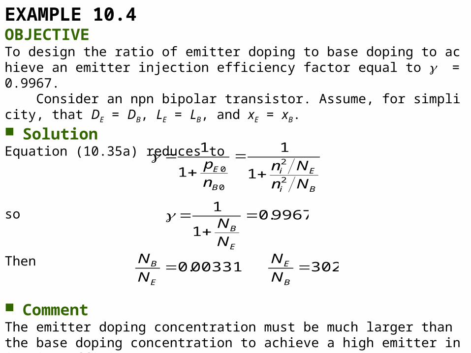
EXAMPLE 10.4OBJECTIVETo design the ratio of emitter doping to base doping to achieve an emitter injection efficiency factor equal to = 0.9967. Consider an npn bipolar transistor. Assume, for simplicity, that DE = DB, LE = LB, and xE = xB. SolutionEquation (10.35a) reduces to
so
Then
CommentThe emitter doping concentration must be much larger than the base doping concentration to achieve a high emitter injection efficiency.
Bi
Ei
B
E
NnNn
np
2
2
0
0 1
1
1
1
9967.01
1
E
B
NN
30200331.0 B
E
E
B
N
N
N
N

EXAMPLE 10.5OBJECTIVETo design the base width required to achieve a base transport factor equal to T = 0.9967. Consider a pnp bipolar transistor. Assume that DB = 10 cm2/s and B0 = 10-7 s. SolutionThe base transport factor applies to both pnp and npn transistors and is given by
Then
We have
so that the base width must then be
CommentIf the base width is less than approximately 0.8 m, then the required base transport factor will be achieved. In most cases, the base transport factor will not be the limiting factor in the bipolar transistor current gain.
9967.0cosh
1
BBT Lx
0814.0B
B
L
x
cm101010 370
BBB DL
m0.814cm10814.0 4 Bx

EXAMPLE 10.6OBJECTIVETo calculate the forward-bias B-E voltage required to achieve a recombination factor equal to = 0.9967. Consider an npn bipolar transistor at T = 300 K. Assume that Jr0 = 10-8 A/cm2 ad that Js0 = 10-11 A/cm2.
SolutionThe recombination factor, from Equation (10.44), is
We then have
We can rearrange this equation and write
Then VBE = 2(0.0259) ln (3.02 105) = 0.654 V
CommentThis example demonstrates that the recombination factor may be an important limiting factor in the bipolar current fain. In this example, if VBE is smaller than 0.654 V, then the recombination factor will fall below the desired 0.9967 value.
kTeV
JJ BE
s
r
2exp1
1
0
0
kTeVBE
2exp
1010
1
19967.0
11
8
53
1002.39967.01
109967.0
2exp
kT
eVBE
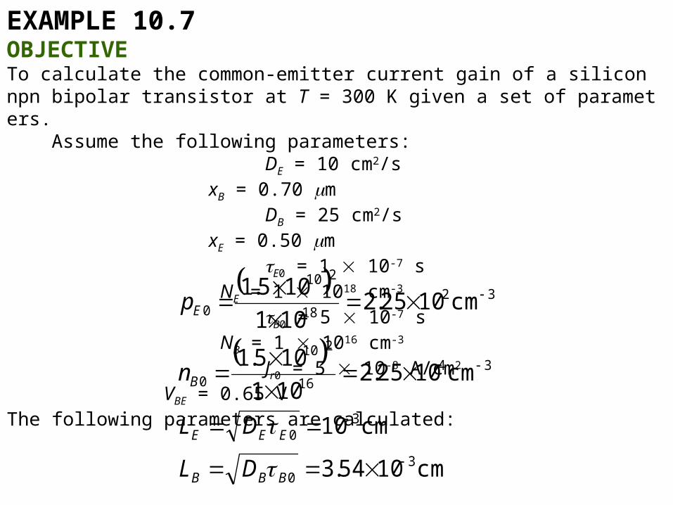
EXAMPLE 10.7OBJECTIVETo calculate the common-emitter current gain of a silicon npn bipolar transistor at T = 300 K given a set of parameters. Assume the following parameters: DE = 10 cm2/s xB = 0.70 m DB = 25 cm2/s xE = 0.50 m E0 = 1 10-7 s NE = 1 1018 cm-3
B0 = 5 10-7 s NB = 1 1016 cm-3
Jr0 = 5 10-8 A/cm2 VBE = 0.65 VThe following parameters are calculated:
cm1054.3
cm10
cm1025.2101
105.1
cm1025.2101
105.1
30
30
3416
210
0
3218
210
0
BBB
EEE
B
E
DL
DL
n
p

SolutionThe emitter injection efficiency factor, from Equation (10.35a), is
The base transport factor, from Equation (10.39a) is
The recombination factor, from Equation (10.44), is
where
9944.0
050.0tanh0198.0tanh
10251025.21054.3101025.2
1
1
34
32
9998.0
1054.31070.0
cosh
1
3
4
T
0259.02065
exp105
1
1
0
8
sJ
2923
4190
0 A/cm1029.110977.1tanh1054.3
1025.225106.1
tanh
B
BB
BBs
Lx
L
neDJ

SolutionWe can now calculate = 0.99986. The common-base current gain is then
= T = (0.9944)(0.9998)(0.99986) = 0.99406which gives a common-emitter current gain of
CommentIn this example, the emitter injection efficiency is the liming factor in the current gain.
16799406.01
99406.0
1

15102
EXAMPLE 10.8OBJECTIVETo calculate the change in the neutral base width with a change in C-B voltage. Consider a uniformly doped silicon bipolar transistor at T = 300 K with a base doping of NB = 5 1016 cm-3 and a collector doping of NC = 2 1015 cm-3. Assume the metallurgical base width is 0.70 m. Calculate the change in the neutral base width as the C-B voltage changes from 2 to 10 V. SolutionThe space chare width extending into the base region can be written as
or
which becomesxdB = [(9.96 10-12)(Vbi + VCB)]1/2
The built-in potential is
21
12
CBB
CCBbisdB NNN
N
e
VVx
21
151616
15
19
14
102105
1
105
102
106.1
1085.87.112
CBbi
dB
VVx
V718.0ln2
i
CBbi n
NN
e
kTV

SolutionFor VCB = 2 V, we find xdB = 0.052 m, and for VCB = 10 V, we find xdB = 0.103 m. If we neglect the B-E space charge region, which will be small because of the forward-biased junction, then we can calculate the neutral base width. For VCB = 2 V.
xB = 0.70 0.052 = 0.648 mand for VCB = 10 V,
xB = 0.70 0.103 = 0.597 m CommentThis example shows that the neutral base width can easily change by approximately 8 percent as the C-B voltage changes from 2 to 10 V.

EXAMPLE 10.9OBJECTIVETo calculate change in collector current with a change in neutral base width, and to estimate the Early voltage. Consider a uniformly doped silicon npn bipolar transistor with parameters described in Example 10.8. Assume DB = 25 cm2/s, and VBE = 0.60 V, and also assume that xB << L
B. SolutionThe excess minority-carrier electron concentration in the base is given by w”quation (10.15) as
If xB << LB, then (xB x) << LB so we can write the approximations
The expression for nB(x) can then be approximated as
B
B
BB
BBEB
B
Lx
Lx
Lxx
kTeV
n
xn
sinh
sinhsinhexp0
B
B
B
B
B
B
B
B
L
xx
L
xx
L
x
L
xsinhandsinh
xxx
kT
eV
x
nxn B
BE
B
BB 1exp0

The collector current is now
The value of nB0 is calculated as
If we let xB = 0.648 m when VCB = 2 V (VCE = 2.6 V), then
Now let xB = 0.597 m when VCB = 10 V (VCE = 10.6 V). In this case we have |JC| = 3.47 A/cm2. From Equation (10.45a), we can write
Using the calculated values of current and voltage, we have
The Early voltage is then determined to be VA 92 V CommentThis example indicates how much the collector current can change as the neutral base width changes with a change in the B-C space charge width, and it also indicates the magnitude of the Early voltage.
kT
eV
x
neD
dx
xndeDJ BE
B
BBBBC exp0
3316
2102
0 cm105.4105
105.1
B
iB N
nn
24
319
A/cm20.30259.0
60.0exp
10648.0
105.425106.1
CJ
AACE
C
CE
C
VVV
J
V
J
6.2
20.3
6.26.10
20.347.3
CE
C
ACE
C
CE
C
V
J
VV
J
dV
dJ

EXAMPLE 10.10OBJECTIVETo determine the increase in pE0 in the emitter due to bandgap narrowing. Consider a silicon emitter at T = 300 K. Assume the emitter doping increases from 1018 cm-3 to 1019 cm-3. Calculate the change in the pE0 value. SolutionFor emitter doping of NE = 1018 cm-3 and 1019 cm-3, we have, neglecting bandgap narrowing.
and
Taking into account the bandgap narrowing, we obtain, respectively, for NE = 1018 cm-3 and NE = 1019 cm-3
and
CommentIf the emitter doping increases from 1018 to 1019 cm-3, the thermal equilibrium minority carrier concentration decreases by approximately a factor of 2 rather than a factor of 10. This effect is due to bandgap narrowing.
3218
2102
0 cm1025.210
105.1
E
iE N
np
3119
210
0 cm1025.210
105.1
Ep
3218
210
0 cm1016.70259.0
030.0exp
10
105.1
Ep
3219
210
0 cm1094.40259.0
08.0exp
10
105.1
Ep

EXAMPLE 10.11OBJECTIVETo determine the effect of emitter current crowding. Consider the geometry shown in Figure 10.33. The base doping concentration is NB = 1016 cm-3, the neutral base width is xB = 0.80 m, the emitter width is S = 10 m, and the emitter length is L = 10 m. (a) Determine the resistance of the base between x = 0 and x = S/2. Assume a hole mobility of p = 400 cm2/V-s. (b) If the base current in this region is uniform and given by IB/2 = 5 A, determine the potential difference between x = 0 and x = S/2. (c) Using the results of part (b), what is the ratio of emitter current density at x = 0 and x = S/2? Solution(a) The resistance is found from
or
R = 9.77 103 = 9.77 k
44
4
1619 1010108.0
105
10400106.1
1
21
Lx
S
NeA
lR
BBp

(b) The potential difference is
or
V = 4.885 10-2 V = 48.85 mV
36 1077.91052
R
IV B
n+ emitter
L
S
xB
x = S/2x = 0
p base
IB/2
n collectorFigure 10.33 Geometry used for Example 10.11 and Exercise Problem EX 10.11.

(c) The ratio of emitter current at x = 0 to that at x = S/2 is found to be
or
CommentBecause the B-E voltage at the emitter edge (x = 0) is larger than that in the center of the emitter (x = S/2), the current at the edge is larger than that in the center of the emitter.
0259.0
04885.0expexp
2
0
tE
E
V
V
SxI
xI
59.6
2
0
SxI
xI
E
E

EXAMPLE 10.12OBJECTIVETo design the collector doping and collector width to meet a punch-through voltage specification. Consider a uniformly doped silicon bipolar transistor with a metallurgical base width of 5 m and a base doping of NB = 1016 cm-3. The punch-through voltage is to be Vpt = 25 V. SolutionThe maximum collector doping concentration can be determined from Equation (10.54) as
or
which yields NC = 8.38 1014 cm-3
This n-type doping concentration in the collector must extend at least as far as the depletion width extends into the collector to avoid breakdown in the collector region. We have, using results from Chapter 5.
C
C
N
N14
1616419
1085.87.112
1010105.0106.125
CN
1610194.12
21
12
CBC
BRbisn NNN
N
e
VVx

Neglecting Vbi compared to VR = Vpt, we obtain
orxn = 5.97 m
CommentFrom Figure 9.30, the expected avalanche breakdown voltage for this junction is greater than 300 V. Obviously punch-through will occur before the normal breakdown voltage in this case. For a larger punch-through voltage, a larger metallurgical base width will be required, since a lower collector doping concentration is becoming impractical. A larger punch-through voltage will also require a larger collector width in order to avoid premature breakdown in this region.
2/1
141614
16
19
14
1038.810
1
1038.8
10
106.1
251085.87.112
nx

EXAMPLE 10.13OBJECTIVETo design a bipolar transistor to meet a breakdown voltage specification. Consider a silicon bipolar transistor with a common-emitter current gain of = 100 and a base doping concentration of NB = 1017 cm-3. The minimum open-base breakdown voltage is to be 15 V. SolutionFrom Equation (10.63), the minimum open-emitter junction breakdown voltage must be
Assuming the empirical constant n is 3, we find
From Figure 9.30, the maximum collector doping concentration should be approximately 7 1015 cm-3 to achieve this breakdown voltage. CommentIn a transistor circuit, the transistor must be designed to operate under a worst-case situation. In this example, the transistor must be able to operate in an open-base configuration without going into breakdown. As we determined previously, an increase in breakdown voltage can be achieved by decreasing the collector doping concentration.
00 CEn
CB BVBV
V6.691510030 CBBV

2
EXAMPLE 10.14OBJECTIVETo determine, to a first approximation, the frequency at which the small-signal current gain decreases to 1/ of its low frequency value. Consider the simplified hybrid-pi circuit shown in Figure 10.42. We are ignoring C, Cs, r, Cje, r0, and the series resistances. We must emphasize that this is a first-order calculation and that C normally cannot be neglected.
SolutionAt very low frequency, we may neglect C so that
Vbe = Ibr and Ic = gmVbe = gmrIb
C rgmVbeVbe
+
B C
E
Ib Ic
Figure 10.42 Simplified hybrid-pi equivalent circuit.

SolutionWe can then write
where hfe0 is the low-frequency, small-signal common-emitter current gain. Taking into account C, we have
Then
or the small-signal current gain can be written as
The magnitude of the current gain drops to 1/ of its low-frequency value at f = 1/2rC. If, for example, r = 2.6 k and C = 4 pF, then
f = 15.3 MHz Commentthe frequency calculated in this example is called the beta cutoff frequency. High-frequency transistors must have small diffusion capacitances, implying the use of small devices.
rgI
Ih m
b
cfe 0
Crj
rIV bbe 1
Crj
hIVgI fe
bbemc 10
Crj
h
I
IA fe
b
ci 1
0
2

EXAMPLE 10.15OBJECTIVETo calculate the emitter-to-collector transit time and the cutoff frequency of a bipolar transistor, given the transistor parameters. Consider a silicon npn transistor at T = 300 K. Assume the following parameters: IE = 1 mA Cje = 1 pF xB = 0.5 m Dn = 25 cm2/s xdc = 2.4 m rc = 25 C = 0.1 pF Cs = 0.1 pF SolutionWe will initially calculate the various time-delay factors. If we neglect the parasitic capacitance, the emitter-base junction charging time is
e = reCje
where
Thene = (25.9)(1012) = 25.9 ps
The base transit time is
9.25101
0259.013
Ee Ie
kTr
ps50252
105.0
2
242
n
Bb D
x

The collector depletion region transit time is
The collector capacitance charging time isc = rc(C + Cs) = (20)(0.2 1012) = 4 ps
The total emitter-to-collector time delay is thenec = 25.9 + 50 + 24 + 4 = 103.9 ps
so that the cutoff frequency is calculated as
If we assume a low-frequency common-emitter current gain of = 100, then the beta cutoff frequency is
CommentThe design of high-frequency transistors requires small device geometries to reduce capacitances and narrow base widths to reduce the base transit time.
GHz53.1109.1032
1
2
112
ecTf
ps2410
104.27
4
s
dcb
x
MHz3.15100
1053.1 9
0
Tff