Embed Size (px)
Citation preview

EWM-C109F6 series
Specifications subject to change without notice, contact your sales representatives for the most update information.
REV 1.4 Page 1 of 66 26.Sep. 2017
EWM-C109F6 series Datasheet

EWM-C109F6 series
Specifications subject to change without notice, contact your sales representatives for the most update information.
REV 1.4 Page 2 of 66 26. Sep. 2017
CONTENTS 1. Functional description ...................................................................... 5
1.1 Overview ......................................................................................................................... 5
1.2 Features .......................................................................................................................... 6
1.3 Block diagram ................................................................................................................. 7
1.4 Product description ......................................................................................................... 8
1.5 AT Command support ..................................................................................................... 9
1.6 AssustNow clients and GPS integration (EWM-C109F6G1E only) ............................... 10
1.7 In-Band modem (EWM-C109F6G1E only) .................................................................... 10
1.8 Smart temperature supervision ..................................................................................... 10
1.9 TCP/IP and UDP/IP ....................................................................................................... 11
1.10 FTP and FTPS .............................................................................................................. 11
1.11 HTTP and HTTPS ......................................................................................................... 11
1.12 Jamming Detection ....................................................................................................... 11
1.13 Hybrid positioning and CellLocate (EWM-C109F6G1E only) ........................................ 12 1.13.1 Positioning through cellular information: CellLocate .......................................................................... 12 1.13.2 Hybrid positioning ............................................................................................................................... 12
2. Mechanical Specifications ............................................................. 14 2.1 Dimensions and interfaces ............................................................................................ 14
2.1.1 RF Antenna guidelines ....................................................................................................................... 18 2.1.2 GPS Antenna guidelines .................................................................................................................... 19
2.2 Antenna connector ........................................................................................................ 19
2.3 Dimensions of the Mini PCI Express Connector ............................................................ 20
3. System description ......................................................................... 22 3.1 Pin assignment .............................................................................................................. 22
3.2 Operating modes ........................................................................................................... 23
3.3 Module supply (VCC) .................................................................................................... 24 3.3.1 VCC application circuits ..................................................................................................................... 26
3.4 Real Time Clock supply input/output (V_BCKP) ............................................................ 27
3.5 System functions ........................................................................................................... 29 3.5.1 Module power-on ................................................................................................................................ 29 3.5.2 Module power-off ................................................................................................................................ 31 3.5.3 Module reset ....................................................................................................................................... 32
3.6 USB interface ................................................................................................................ 33 3.6.1 USB features ...................................................................................................................................... 34 3.6.2 USB application circuit ....................................................................................................................... 35
3.7 Serial communication .................................................................................................... 35 3.7.1 Serial interfaces configuration ............................................................................................................ 36 3.7.2 Asynchronous serial interface (UART) ............................................................................................... 37 3.7.3 UART features .................................................................................................................................... 38 3.7.4 UART signal behavior (AT commands interface case) ....................................................................... 40
3.8 (U)SIM interface ............................................................................................................ 44
3.9 Audio Interface .............................................................................................................. 45 3.9.1 I
2S interface - PCM mode ................................................................................................................... 47
3.9.2 I2S interface - Normal I
2S mode ......................................................................................................... 48
3.10 Network status indication .............................................................................................. 48
4. Electrical specifications ................................................................. 50 4.1 Maximum ESD .............................................................................................................. 50
4.2 Operating conditions ..................................................................................................... 50
EWM-C109F6 series
Specifications subject to change without notice, contact your sales representatives for the most update information.
REV 1.4 Page 3 of 66 26. Sep. 2017
4.2.1 Operating temperature range ............................................................................................................. 50 4.2.2 Supply/Power pins .............................................................................................................................. 51 4.2.3 Power consumption ............................................................................................................................ 51 4.2.4 RF Performance ................................................................................................................................. 53 4.2.5 RESET_N pin ..................................................................................................................................... 55 4.2.6 (U)SIM pins ......................................................................................................................................... 55 4.2.7 AC characteristics of digital audio interfaces pins .............................................................................. 56
Appendix: Part Number Table ........................................................... 66

EWM-C109F6 series
Specifications subject to change without notice, contact your sales representatives for the most update information.
REV 1.4 Page 4 of 66 26. Sep. 2017
Revision History
Rev. Date History
1.0 2012/07/11 1. 1st release
1.1 2012/10/05 1. Modify Mechanical and pin define
1.2 2014/4/30 1. Modify the height of component
1.3 2014/6/9 1. Modify the pin definition
1.4 2017/9/26 1. Update module label for new CE RED
Advantech reserves the right to make changes without further notice to any products or data herein to improve reliability, function, or
design. Information furnished by Advantech is believed to be accurate and reliable. However, Advantech does not assure any liability
arising out of the application or use of this information, nor the application or use of any product or circuit described herein, neither
does it convey any license under its patent rights nor the rights of others.
Copyright © 1983-2014 Advantech Co., Ltd. All rights reserved.

EWM-C109F6 series
Specifications subject to change without notice, contact your sales representatives for the most update information.
REV 1.4 Page 5 of 66 26. Sep. 2017
1. Functional description
1.1 Overview
The EWM-C109F601E is base on U-blox LISA-U200 and the EWM-C109F6G1E is a
combination of U-blox LISA-U200 and GPS MAX-6 module.
The EWM-C109F6 HSPA series (EWM-C109F601E and EWM-C109F6G1E) mini PCIE
module with an integrated SIM holder is ideal for consumer and industrial applications requiring
high-speed data transmission rates, and machine-to-machine applications. They are the perfect
choice for mobile Internet terminals, tablets, in-car infotainment, connected navigation systems,
security and surveillance system, eCall, fleet management, metering, anti-theft systems, and
other automotive applications.
The EWM-C109F6 HSPA series modules with 6-band WCDMA(UMTS) and quad-band
GSM/GPRS/EDGE are suited for networks worldwide. Featuring 7.2 Mb/s HSDPA downlink and
5.76 Mb/s HSUPA uplink speeds, a rich set of Internet protocols, and very low power
consumption and extended operating temperature range.
EWM-C109F6G1E module provides fully integrated access to u-blox GPS receivers.
Wireless and GPS are controlled through a single serial port from any host processor.

EWM-C109F6 series
Specifications subject to change without notice, contact your sales representatives for the most update information.
REV 1.4 Page 6 of 66 26. Sep. 2017
1.2 Features
Module Technology Bands Interface Audio Function
HSU
PA
[M
b/s
]
HSD
PA
[M
b/s
]
UM
TS/H
SPA
[M
Hz]
GP
RS/
EDG
E q
uad
-ban
d
UA
RT
USB
U.F
L-R
-SM
T 5
0Ω
an
ten
na
con
nec
tor
UIC
C/S
IM c
ard
inte
rfac
e
An
alo
g A
ud
io
Dig
ital
Au
dio
(4
-wir
e I2
C)
GP
S /
A-G
PS
Inte
grat
ed S
IM h
old
er
Net
wo
rk in
dic
atio
n
Emb
edd
ed T
CP
/UD
P
FTP
, H
TTP
SSL
Ass
istN
ow
so
ftw
are
FW u
pd
ate
via
ser
ial
EWM
-C1
09
F60
1E
5.7
6
7.2
80
0/8
50
/90
0/
17
00
/19
00
/21
00
1
1
1
1
EWM
-C1
09F6
G1
E
5.7
6
7.2
800
/850
/900
/ 1
700/
1900
/21
00
1 1 2 1

EWM-C109F6 series
Specifications subject to change without notice, contact your sales representatives for the most update information.
REV 1.4 Page 7 of 66 26. Sep. 2017
VCC 4.2V USB_DET 5.0V
GPIO
MAX-6G
VCC 1.8V
LISA-U200
USB
UART
Digital Audio (I
2S)
V_BCKP (RTC)
External Reset
VCC 3.8V
VCC 3.3V
VCC 5V For USB_D
I2C
(DCC) GPIO
USIM
MAX-6G
VCC 1.8V
1.3 Block diagram
Note : EWM-C109F601E model does not include MAX-6G GPS block.
PC
I exp
ress m
ini c
ard
SIM slot
DC/DC converter

EWM-C109F6 series
Specifications subject to change without notice, contact your sales representatives for the most update information.
REV 1.4 Page 8 of 66 26. Sep. 2017
1.4 Product description
The EWM-C109F6 HSPA series modules integrate full-feature 3G UMTS/HSxPA
and 2G GSM/GPRS/ EDGE with integrated SIM holder and compatible Mini PCIE spec.
standard interface revision 1.0 & 1.2. The EWM-C109F6G1E module protocol stack
with Assisted GPS support.
Table 1 EWM-C109F6 HSPA series module UMTS/HSDPA/HSUPA and GSM/GPRS/EDGE characteristics
3G UMTS/HSDPA/HSUPA Characteristics 2G GSM/GPRS/EDGE Characteristics
Class A User Equipment1 Class B Mobile Station
2
UMTS Terrestrial Radio Access (UTRA) Frequency Division Duplex (FDD) operating mode
Six-band support: Band I (2100 MHz), Band II (1900 MHz),
Band IV (1700 MHz), Band V (850 MHz), Band VI (800 MHz), Band VIII (900 MHz)
Quad-band support GSM 850 MHz, E-GSM 900 MHz, DCS 1800 MHz, PCS 1900 MHz
WCDMA/HSDPA/HSUPA Power Class Power Class 3 (24 dBm) for WCDMA/HSDPA/
HSUPA mode
GSM/GPRS Power Class 4 (33 dBm) for GSM/E-GSM bands
Power Class 1 (30 dBm) for DCS/PCS bands
EDGE Power Class Power Class E2 (27 dBm) for GSM/E-GSM
bands Power Class E2 (26 dBm) for DCS/PCS bands
PS (Packet Switched) Data Rate HSUPA category 6, up to 7.2 Mb/s DL, 5.76 Mb/s
UL HSDPA category 8, up to 7.2 Mb/s DL, 384 kb/s
UL
WCDMA PS data up to 384 kb/s DL/UL
PS (Packet Switched) Data Rate GPRS multislot class 33
3, coding scheme
CS1-CS4, up to 107kb/s DL, 85.6kb/s UL EDGE multislot class 33
3, coding scheme
MCS1- MCS9, up to 296kb/s DL, 236.8 kb/s UL
CS (Circuit Switched) Data Rate
WCDMA CS data up to 64 kb/s DL/UL
CS (Circuit Switched) Data Rate GSM CS data up to 9.6kb/s DL/UL supported in
transparent/non transparent mode
Operation modes I to III are supported on GSM/GPRS network, with user-defined preferred service selectable from GSM to GPRS. Paging messages for GSM calls can be optionally monitored during GPRS data transfer in not-coordinating NOM II-III.
The network automatically configures the number of timeslots used for reception or
transmission (voice calls take precedence over GPRS traffic) and channel encoding
(CS1 to MCS9). The maximum (E)GPRS bit rate of the mobile station depends on the
coding scheme and number of time slots. Direct Link mode is supported for TCP and
UDP sockets.
EWM-C109F6 series
Specifications subject to change without notice, contact your sales representatives for the most update information.
REV 1.4 Page 9 of 66 26. Sep. 2017
1 Note : Device can work simultaneously in Packet Switch and Circuit Switch mode: voice calls are possible while the data connection is active without any interruption in service.
2 Note : Device can be attached to both GPRS and GSM services (i.e. Packet Switch and Circuit Switch mode) using one service at a time. If for example during data transmission an incoming call occurs, the data connection is suspended to allow the voice communication. Once the voice call has terminated, the data service is resumed.
3 Note : GPRS/EDGE multislot class 12 implies a maximum of 5 slots in DL (reception) and 4 slots in UL (transmission) with 6 slots in total. GPRS class determines the number of timeslots available for upload and download and thus the speed at which data can be transmitted and received, with higher classes typically allowing faster data transfer rates.
Table 2: Basic Features, Supplementary Services, and Short Message Service (SMS)
Basic features4 Supplementary services Short Message Service (SMS)
Display of Called Number Call Hold/Resume (CH) SMS Classes 1, 2, 3
Indication of Call Progress Signals Call Waiting (CW) Mobile-Originating SMS (MO SMS)
Country/PLMN Indication Multi-Party (MTPY) Mobile-Terminating SMS (MT SMS)
International Access Function Call Forwarding (CF) SMS Cell Broadcast (SMS CB)
Service Indicator Call Divert Text and PDU mode supported
Dual Tone Multi Frequency (DTMF) Explicit Call Transfer (ECT) SMS during circuit-switched calls
Subscription Identity Management Call Barring (CB) SMS over PSD or CSD
Service Provider Indication Call Completion to Busy Subscriber (CCBS)
SMS storage on SIM and memory module
Abbreviated Dialing Advice of Charge Charging (AOCC)
SIM Toolkit Calling Line Identification Presentation (CLIP)
Calling Line Identification Restriction (CLIR)
Connected Line Identification Presentation (COLP)
Connected Line Identification Restriction (COLR)
Unstructured Supplementary Services Data (USSD)
Network Identify and Time Zone (NITZ)
4 Note : These functionalities are supported via AT commands (for more details see the u-blox AT Commands Manual [5]).
1.5 AT Command support
The module supports AT commands according to 3GPP standards: TS 27.007 [1],
27.005 [2], 27.010 [3], and the u-blox AT command extension.
For the complete list of the supported AT commands and their syntax see the u-blox AT Commands Manual [5].

EWM-C109F6 series
Specifications subject to change without notice, contact your sales representatives for the most update information.
REV 1.4 Page 10 of 66 26. Sep. 2017
1.6 AssustNow clients and GPS integration (EWM-C109F6G1E only)
EWM-C109F6G1E module feature embedded AssistNow Online and AssistNow
Offline clients. AssistNow A-GPS provides better GPS performance and faster
Time-To-First-Fix. The clients can be enabled / disabled with an AT command.
The wireless modules act as a stand-alone AssistNow client, making AssistNow
available with no additional requirements for resources or software integration on an
external host micro controller.
This means that GSM/WCDMA and GPS can be controlled through a single serial
port from any host processor.
1.7 In-Band modem (EWM-C109F6G1E only)
EWM-C109F6G1E supports In-Band modem for eCall, according to the 3GPP TS
26.267 specification [8]. According to the eCall (Pan-European automatic in-vehicle
emergency call system) specification, an eCall must be generated automatically or
manually following a car accident, using GSM cellular service “112”. When activated, the
in-vehicle eCall system (IVS) creates an emergency call carrying both voice and data
(e.g. vehicle GPS position) directly to the nearest 112 Public Safety Answering Point
(PSAP) to quickly decide upon detaching rescue services to the known position.
In-Band modem diagram flow
In-band modem allows the fast and reliable transmission of vehicle Minimum Set of
Data (MSD - 140 bytes) and the establishment of a voice emergency call using the same
physical channel (voice channel) without any modifications of the existing cellular
network architecture. In-Band modem is a mandatory feature to meet the eCall
requirements and to develop in vehicle devices fully supporting eCall.
1.8 Smart temperature supervision
An internal sensor is used to constantly monitor the board temperature of The
EWM-C109F6 HSPA series modules. The measured value is compared with the
internally predefined thresholds and it accordingly proceeds. A shutdown is notified and

EWM-C109F6 series
Specifications subject to change without notice, contact your sales representatives for the most update information.
REV 1.4 Page 11 of 66 26. Sep. 2017
automatically forced by the module when the temperature value is outside the specified
range (i.e. the module is in a dangerous working condition). For security reasons the
shutdown is suspended in case of emergency call in progress: in this case the device will
switch off at call termination. The Smart Temperature Supervisor feature can be enabled
or disabled via an AT command (for more details please to u-blox AT commands manual
[5], +USTS AT command). If the feature is disabled there is no embedded protection
against not allowed temperature working conditions.
The sensor measures the board temperature inside the shields, which can differ from ambient temperature.
1.9 TCP/IP and UDP/IP
Via AT commands it is possible to access the TCP/IP and UDP/IP functionalities
over the Packet Switched Data (PSD) connection. For more details about AT commands
see the u-blox AT Commands Manual [5].
Direct Link mode for TCP and UDP sockets is supported. Sockets can be set in
Direct Link mode to establish a transparent end to end communication with an already
connected TCP or UDP socket via serial interface.
1.10 FTP and FTPS
The EWM-C109F6 HSPA series modules support the File Transfer Protocol as well
as Secure File Transfer Protocol functionalities via AT commands. Files are read and
stored in the local file system of the module. For more details about AT commands see
u-blox AT Commands Manual [5].
1.11 HTTP and HTTPS
HTTP and HTTPS client are implemented in EWM-C109F6 series
(EWM-C109F601E and EWM-C109F6G1E) modules. HEAD, GET, POST, DELETE and
PUT operations are available. The file size to be uploaded or downloaded depends on
the free space available in the local file system (FFS) at the moment of the operation. Up
to 4 client contexts can be simultaneously used.
For more details about AT commands see the u-blox AT Commands Manual [5].
1.12 Jamming Detection
In real network situations, modules can experience various out-of-coverage
conditions: limited service conditions when roaming to networks not supporting the
specific SIM, limited service in cells which are not suitable or barred due to operators’
choices, no cell conditions when moving to poorly served or highly interfered areas. In
the latter case, interference can be artificially injected in the environment by a noise
generator covering a given spectrum, thus obscuring the operator’s carriers entitled to
give access to the GSM/UMTS service.

EWM-C109F6 series
Specifications subject to change without notice, contact your sales representatives for the most update information.
REV 1.4 Page 12 of 66 26. Sep. 2017
The Jamming Detection Feature detects such “artificial” interference and reports the
start and stop of such conditions to the client, which can react appropriately by e.g.
switching off the radio transceiver in order to reduce power consumption and monitoring
the environment at constant periods.
The jamming detection feature can be enabled and configured by the +UCD AT
command (for more details refer to the u-blox AT Commands Manual [5]).
1.13 Hybrid positioning and CellLocate (EWM-C109F6G1E only)
Although GPS is a widespread technology, its reliance on the visibility of extremely
weak GPS satellite signals means that positioning is not always possible. Especially
difficult environments for GPS are indoors, in enclosed or underground parking garages,
as well as in urban canyons where GPS signals are blocked or jammed by multipath
interference. The situation can be improved by augmenting GPS receiver data with
cellular network information to provide positioning information even when GPS reception
is degraded or absent. This additional information can benefit numerous applications.
1.13.1 Positioning through cellular information: CellLocate
CellLocate, from u-blox, enables the estimation of device position based on the
parameters of the mobile network cells visible to the specific device. To estimate its
position the u-blox wireless module sends the CellLocate server the parameters of
network cells visible to it using a UDP connection. In return the server provides the
estimated position based on the CellLocate database. The u-blox wireless module can
either send the parameters of the visible home network cells only (normal scan) or the
parameters of all surrounding cells of all mobile operators (deep scan).
CellLocate is implemented using a set of two AT commands that allow configuration
of the CellLocate service (AT+ULOCCELL) and requesting position according to the user
configuration (AT+ULOC). The answer is provided in the form of an unsolicited AT
command including latitude, longitude and estimated accuracy.
Normal scan is only possible in 2G mode.
1.13.2 Hybrid positioning
With u-blox Hybrid positioning technology, u-blox wireless devices can be triggered
to provide their current position using either a u-blox GPS receiver or the estimated
position from CellLocate. The choice depends on which positioning method provides the
best and fastest solution according to the user configuration, exploiting the benefit of
having multiple and complementary positioning methods.
Hybrid positioning is implemented through a set of three AT commands that allow
configuration of the GPS receiver (AT+ULOCGNSS), configuration of the CellLocate
service (AT+ULOCCELL), and requesting the position according to the user configuration
(AT+ULOC). The answer is provided in the form of an unsolicited AT command including

EWM-C109F6 series
Specifications subject to change without notice, contact your sales representatives for the most update information.
REV 1.4 Page 13 of 66 26. Sep. 2017
latitude, longitude and estimated accuracy (if the position has been estimated by
CellLocate), and additional parameters if the position has been computed by the GPS
receiver.
u-blox is extremely mindful of user privacy. When a position is sent to the CellLocate server u-blox is unable to track the SIM used or the specific device.

EWM-C109F6 series
Specifications subject to change without notice, contact your sales representatives for the most update information.
REV 1.4 Page 14 of 66 26. Sep. 2017
2. Mechanical Specifications
2.1 Dimensions and interfaces
The dimension of EWM-C109F601E module is 50.85mm(length) x 29.9mm(width) x
6.2mm(height), Figure 2-1-1 shows the dimensions of EWM-C109F601E module in
details.
Figure 2-1-1 Dimensions of EWM-C109F601E module

EWM-C109F6 series
Specifications subject to change without notice, contact your sales representatives for the most update information.
REV 1.4 Page 15 of 66 26. Sep. 2017
The dimension of EWM-C109F6G1E module is 50.85mm(length) x 29.9mm(width) x
6.7mm(height) Figure 2-1-2 shows the dimensions of EWM-C109F6G1E module in
details.
Figure 2-1-2 Dimensions of EWM-C109F601E module

EWM-C109F6 series
Specifications subject to change without notice, contact your sales representatives for the most update information.
REV 1.4 Page 16 of 66 26. Sep. 2017
Figure 2-1-3 Appearance of the interfaces on EWM-C109F6 HSPA series module

EWM-C109F6 series
Specifications subject to change without notice, contact your sales representatives for the most update information.
REV 1.4 Page 17 of 66 26. Sep. 2017

EWM-C109F6 series
Specifications subject to change without notice, contact your sales representatives for the most update information.
REV 1.4 Page 18 of 66 26. Sep. 2017
① Mini PCI Express connector – It’s used to connect EWM-C109F6 HSPA
series modules to the WWAN Mini PCI Express interface of the PC.
② RF main antenna connector
③ GPS antenna connector
④ SIM holder
2.1.1 RF Antenna guidelines
Antenna characteristics are essential for good functionality of the module. Antenna
radiating performance has direct impact on the reliability of connections over the Air
Interface. A bad termination of the ANT pin (main RF input/output) can result in poor
performance of the module. The following parameters should be checked:

EWM-C109F6 series
Specifications subject to change without notice, contact your sales representatives for the most update information.
REV 1.4 Page 19 of 66 26. Sep. 2017
Table 2-1-1 General recommendation for GSM/UMTS antenna
2.1.2 GPS Antenna guidelines
The modules are designed for use with passive and active antennas.
Table 2-1-2 Antenna Specifications for GPS antenna
Parameter Specification
Antenna Type Active antenna
Active Antenna Recommendations
Minimum gain Maximum gain Maximum noise figure
15 dB (to compensate signal loss in RF cable) 50 dB 1.5 dB
2.2 Antenna connector
The antenna connector type used is a U.FL microwave coaxial connector. It is also
can be used for testing purpose.
Item Recommendations
Impedance 50 Ω nominal characteristic impedance
Frequency Range
824..960 MHz (GSM 850, GSM 900, UMTS B5, UMTS B6, UMTS B8)
1710..2170 MHz (GSM 1800, GSM 1900, UMTS B1, UMTS B2, UMTS B4)
Input Power >2 W peak
V.S.W.R <2:1 recommended, <3:1 acceptable
Return Loss S11<-10 dB recommended, S11<-6 dB acceptable
Gain <3 dBi

EWM-C109F6 series
Specifications subject to change without notice, contact your sales representatives for the most update information.
REV 1.4 Page 20 of 66 26. Sep. 2017
2.3 Dimensions of the Mini PCI Express Connector
The EWM-C109F6 HSPA series modules adopt a standard mini PCIE connector
that has 52 pins and complies with the PCIE mini card electromechanical specification
revision 1.2.
Figure 2-3-1 show a 52-pin Mini PCI Express connector for The EWM-C109F6
HSPA series module use. (take the ChiTek AKP-3B0A-052-3 as an example).

EWM-C109F6 series
Specifications subject to change without notice, contact your sales representatives for the most update information.
REV 1.4 Page 21 of 66 26. Sep. 2017
Figure 2-3-1 Dimensions of the Mini PCI Express connector

EWM-C109F6 series
Specifications subject to change without notice, contact your sales representatives for the most update information.
REV 1.4 Page 22 of 66 26. Sep. 2017
3. System description
3.1 Pin assignment
PIN No. Name Describe PIN No. Name Describe
1 NC
2 VCC I , Module supply input
3 RI 4 GND
5 NC 6 NC
7 NC 8 UIM_PWR O , SIM supply output 1.8/3.0V
9 GND 10 UIM_DATA I/O ,SIM data
11 NC 12 UIM_CLK O , SIM clock
13 NC 14 UIM_RESET O , SIM reset
15 GND 16 NC
17 V_BCKP I/O , Real time clock supply inpot/output
18 GND
19 NC 20 NC
21 GND 22 RESET_N I , External reset input
23 NC
24 VCC I , Module supply input
25 NC 26 GND
27 GND 28 NC
29 GND 30 NC
31 NC 32 NC
33 NC
34 GND
35 GND 36 USB_D- I/O , USB data line D-
37 GND 38 USB_D+ USB , USB data line D+
39 VCC I , Module supply input 40 GND
41 VCC I , Module supply input 42 LED_WAN# O , Network status indication
43 GND 44 NC
45 I2S_CLK O , I2S clock 46 NC
47 I2S_TXD O , I2S transmit data 48 NC
49 I2S_RXD I , I2S receive data 50 GND
51 I2S_WA O , I2S word alignment 52 VCC I , Module supply input

EWM-C109F6 series
Specifications subject to change without notice, contact your sales representatives for the most update information.
REV 1.4 Page 23 of 66 26. Sep. 2017
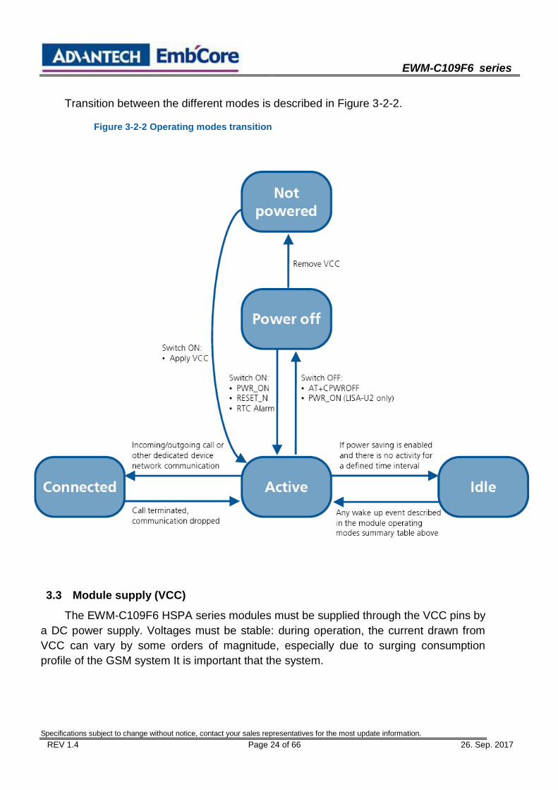
3.2 Operating modes
The EWM-C109F6 HSPA series modules have several operating modes.
Table 3-2-1 summarizes the various operating modes and provides general guidelines for operation.
EWM-C109F6 series
Specifications subject to change without notice, contact your sales representatives for the most update information.
REV 1.4 Page 24 of 66 26. Sep. 2017
Transition between the different modes is described in Figure 3-2-2.
Figure 3-2-2 Operating modes transition
3.3 Module supply (VCC)
The EWM-C109F6 HSPA series modules must be supplied through the VCC pins by
a DC power supply. Voltages must be stable: during operation, the current drawn from
VCC can vary by some orders of magnitude, especially due to surging consumption
profile of the GSM system It is important that the system.

EWM-C109F6 series
Specifications subject to change without notice, contact your sales representatives for the most update information.
REV 1.4 Page 25 of 66 26. Sep. 2017
Table 3-3 Module supply pins
Name Description Remarks VCC Module power supply input VCC pins are internally connected, but all the
available pads must be connected to the external supply in order to minimize the power loss due to series resistance. Clean and stable supply is required: low ripple and low voltage drop must be guaranteed. Voltage provided must always be above the minimum limit of the operating range. Consider that during a GSM call there are large current spikes in connected mode.
GND Ground GND pins are internally connected but a good (low impedance) external ground can improve RF performance: all available pads must be connected to ground.
VCC pins ESD sensitivity rating is 1 kV (Human Body Model according to JESD22-A114F). Higher protection level can be required if the line is externally accessible on the application board. Higher protection level can be achieved by mounting an ESD protection (e.g. EPCOS CA05P4S14THSG varistor array) on the line connected to this pin.
The voltage provided to the VCC pins must be within the normal operating range
limits as specified in the EWM-C109F6 HSPA series Data Sheet. Complete functionality
of the module is only guaranteed within the specified minimum and maximum VCC
voltage normal operating range.
The module cannot be switched on if the VCC voltage value is below the specified normal operating range minimum limit: ensure that the input voltage at VCC pins is above the minimum limit of the normal operating range for more than 1 s after the start of the switch-on of the module.
When EWM-C109F6 HSPA series modules are in operation, the voltage provided to
VCC pins can go outside the normal operating range limits but must be within the
extended operating range limits specified in ZU200 series DataSheet. Occasional
deviations from the ETSI specifications may occur when the input voltage at VCC pins is
outside the normal operating range and is within the extended operating range.
The EWM-C109F6 HSPA series modules switch off when VCC voltage value drops below the specified extended operating range minimum limit: ensure that the input voltage at VCC pins never drops below the minimum limit of the extended operating range when the module is switched on, not even during a

EWM-C109F6 series
Specifications subject to change without notice, contact your sales representatives for the most update information.
REV 1.4 Page 26 of 66 26. Sep. 2017
GSM transmit burst, where the current consumption can rise up to maximum peaks of 2.5 A in case of a mismatched antenna load.
Operation above the normal operating range maximum limit is not recommended and extended exposure beyond it may affect device reliability.
Stress beyond the VCC absolute maximum ratings can cause permanent damage to the module: if necessary, voltage spikes beyond VCC absolute maximum ratings must be restricted to values within the specified limits by using appropriate protection.
3.3.1 VCC application circuits
The power supply of EWM-C109F6 HSPA series module has to be a single voltage
source in the range of VCC = 3.3V~3.6V. It must be able to with stand a sufficient current
in a transmission burst which typically rises to 2.5A. Beyond that, the power supply must
be able to account for increased current consumption if the module is exposed to
inappropriate conditions, for example antenna mismatch.
For the VCC input, a local bypass capacitor is recommended. A capacitor (about
1500μF, low ESR) is recommended. A lower cost choice may be a 1500 μF tantalum
capacitor (low ESR) with a small (1 μF to 10μF) ceramic in parallel, which is illustrated as
following figure. And the capacitors should be put as closer as possible to EWM-C109F6
HSPA series module VCC pins. The following figure is the recommended circuit.
Figure 3-3-1: VCC input
When designing the power supply for your application, special attention should be
paid on power losses. Please ensure VCC never drops below 3.0V on the EWM-C109F6
HSPA series modules, not even in a transmit burst where current consumption can rise
to typical peaks of 2.5 A. If the power voltage drops below 3.0V, the module may be

EWM-C109F6 series
Specifications subject to change without notice, contact your sales representatives for the most update information.
REV 1.4 Page 27 of 66 26. Sep. 2017
switched off.
3.4 Real Time Clock supply input/output (V_BCKP)
The V_BCKP pin connects the supply for the Real Time Clock (RTC) and Power-On
/ Reset internal logic. This supply domain is internally generated by a linear regulator
integrated in the power Management Unit. The output of this linear regulator is always
enabled when the main voltage supply provided to the module through VCC is within the
valid operating range, with the module switched-off or powered-on.
Table 3-4-1 Real Time Clock supply pin
Name Description Remarks
V_BCKP Real Time Clock
supply
V_BCKP output voltage = 1.8 V (typical) on
EWM-C109F6 HSPA series generated by the
module to supply Real Time Clock whenVCC
supply voltage is within valid operating range.
The RTC provides the time reference (date and time) of the module, also in
power-off mode, when the V_BCKP voltage is within its valid range (specified in the Input
characteristics of Supply/Power pins table in EWM-C109F6 HSPA series modules. The
RTC timing is normally used to set the wake-up interval during idle-mode periods
between network paging, but is able to provide programmable alarm functions by means
of the internal 32.768 kHz clock.
The RTC can be supplied from an external back-up battery through the V_BCKP,
when the main voltage supply is not provided to the module through VCC. This lets the
time reference (date and time) run until the V_BCKP voltage is within its valid range,
even when the main supply is not provided to the module.
The RTC oscillator doesn't necessarily stop operation (i.e. the RTC counting doesn't
necessarily stop) when V_BCKP voltage value drops below the specified operating range
minimum limit (1.00 V): the RTC value read after a system restart could be not reliable as
explained in the following Table 3-4-2.

EWM-C109F6 series
Specifications subject to change without notice, contact your sales representatives for the most update information.
REV 1.4 Page 28 of 66 26. Sep. 2017
Table3-4-2 RTC value reliability as function of V_BCKP voltage value
Consider that the module cannot switch on if a valid voltage is not present on VCC
even when the RTC is supplied through V_BCKP (meaning that VCC is mandatory to
switch-on the module). The RTC has very low power consumption, but is highly
temperature dependent. For example at 25°C, with the V_BCKP voltage equal to the
typical output value, the power consumption is approximately 2 μA, whereas at 70°C and
an equal voltage the power consumption increases to 5-10 μA.
If V_BCKP is left unconnected and the module main voltage supply is removed from
VCC, the RTC is supplied from the bypass capacitor mounted inside the module.
However, this capacitor is not able to provide a long buffering time: within few
milliseconds the voltage on V_BCKP will go below the valid range (1 V min). This has no
impact on wireless connectivity, as all the functionalities of the module do not rely on
date and time setting.
If RTC is required to run for a time interval of T [s] at 25°C when VCC supply is
removed, place a capacitor with a nominal capacitance of C [μF] at the V_BCKP pin.
Choose the capacitor using the following formula:
C [μF] = (Current_Consumption [μA] x T [s]) / Voltage_Drop [V]
= 2.50 x T [s] for EWM-C109F6 HSPA series
For example, a 100 μF capacitor (such as the Murata GRM43SR60J107M) can be
placed at V_BCKP to provide a long buffering time. This capacitor will hold V_BCKP
voltage within its valid range for around 50 s at 25°C, after the VCC supply is removed. If
a very long buffering time is required, a 70 mF super-capacitor (e.g. Seiko Instruments
XH414H-IV01E) can be placed at V_BCKP, with a 4.7 k series resistor to hold the
V_BCKP voltage within its valid range for approximately 10 hours at 25°C, after the VCC
supply is removed. The purpose of the series resistor is to limit the capacitor charging
current due to the large capacitor specifications, and also to let afast rise time of the
voltage value at the V_BCKP pin after VCC supply has been provided. These capacitors
will allow the time reference to run during battery disconnection.
V_BCKP voltage value RTC value reliability Notes
1.00 V < V_BCKP < 1.90 V RTC oscillator doesn't stop operation V_BCKP within operating range
0.05 V < V_BCKP < 1.00 V RTC oscillator doesn't necessarily stop operation
V_BCKP below operating range
RTC value read after a restart of the system is not reliable
0.00 V < V_BCKP < 0.05 V RTC oscillator stops operation V_BCKP below operating range
RTC value read after a restart of the system is reliable

EWM-C109F6 series
Specifications subject to change without notice, contact your sales representatives for the most update information.
REV 1.4 Page 29 of 66 26. Sep. 2017
Figure 3-4-3 : Real time clock supply (V_BCKP) application circuits
(a) using a 100 μF capacitor to let the RTC run for ~50 s after VCC removal;
(b) using a 70 mF capacitor to let RTC run for ~10 hours after VCC removal;
(c) using a non-rechargeable battery
Table 3-4-4: Example of components for V_BCKP buffering
Reference Description Part Number -Manufacturer
C1 100 μF Tantalum Capacitor GRM43SR60J107M -Murata
R2 4.7 kΩ Resistor 0402 5% 0.1 W RC0402JR-074K7L -Yageo Phycomp
C2 70 mF Capacitor XH414H-IV01E -Seiko Instruments
3.5 System functions
3.5.1 Module power-on
The power-on sequence of EWM-C109F6 HSPA series modules is initiated in one of
these ways:
Rising edge on the VCC pin to a valid voltage as module supply (i.e.
applying module supply)
Rising edge on the RESET_N pin (i.e. releasing from low level the pin,
normally high by internal pull-up)
RTC alarm (i.e. pre-programmed scheduled time by AT+CALA command)
3.5.1.1. Rising edge on VCC
When a supply is connected to VCC pins, the module supply supervision circuit
controls the subsequent activation of the power up state machines: the module is
switched on when the voltage rises up to the VCC normal operating range minimum limit
starting from a voltage value lower than 2.25 V
The voltage at the VCC pins must ramp from 2.5 V to 3.2 V within 1 ms to

EWM-C109F6 series
Specifications subject to change without notice, contact your sales representatives for the most update information.
REV 1.4 Page 30 of 66 26. Sep. 2017
switch on the module.
3.5.1.2. Rising edge on RESET_N
EWM-C109F6 HSPA series modules can be switched on by means of the
RESET_N input pin: the RESET_N signal must be forced low for at least 50 ms and then
released to generate a rising edge that starts the module power-on sequence.
RESET_N input pin can also be used to perform an “external” or “hardware” reset of
the module, as described in the section 3.4.3.
Electrical characteristics of the EWM-C109F6 HSPA series RESET_N input are
slightly different from the other digital I/O interfaces: the pin provides different input
voltage thresholds. RESET_N is pulled high to V_BCKP by an integrated pull-up
resistor also when the module is in power-off mode. Therefore an external pull-up is not
required on the application board.
The simplest way to switch on the module by means of the RESET_N input pin is to
use a push button that shorts the RESET_N pin to ground: the module will be switched
on at the release of the push button, since the RESET_N will be forced to the high level
by the integrated pull-up resistor, generating a rising edge.
If RESET_N is connected to an external device (e.g. an application processor on an
application board) an open drain output can be directly connected without any external
pull-up. A push-pull output can be used too: in this case make sure that the high level
voltage of the push-pull circuit is below the maximum voltage operating range of the
RESET_N pin. To avoid unwanted power-on or reset of the module make sure to fix the
proper level at the RESET_N input pin in all possible scenarios.
3.5.1.3. Real Time Clock (RTC) alarm
If a voltage within the operating range is maintained at the VCC pin, the module can
be switched on by the RTC alarm when the RTC system reaches a pre-programmed
scheduled time (refer to the u-blox AT Commands Manual [3], AT+CALA command). The
RTC system will then initiate the boot sequence by instructing the Power Management
Unit to turn on power. Also included in this setup is an interrupt signal from the RTC
block to indicate to the baseband processor that an RTC event has occurred.
3.5.1.4. Additional considerations
The module is switched on when the VCC voltage rises up to the normal operating
range (i.e. applying module supply): the first time that the module is used, it is switched
on in this way. Then, EWM-C109F6 HSPA series modules can be switched off by means
of the AT+CPWROFF command. When the module is in power-off mode, i.e. the
AT+CPWROFF command has been sent and a voltage value within the normal operating
range limits is still provided to the VCC pin, the digital input-output pads of the baseband

EWM-C109F6 series
Specifications subject to change without notice, contact your sales representatives for the most update information.
REV 1.4 Page 31 of 66 26. Sep. 2017
chipset (i.e. all the digital pins of the module) are locked in tri-state (i.e. floating). The
power down tri-state function isolates the module pins from its environment, when no
proper operation of the outputs can be guaranteed.
The module can be switched on from power-off mode by forcing a proper start-up
event (i.e. low level on the PWR_ON pin, or an RTC alarm). After the detection of a
start-up event, all the digital pins of the module are held in tri-state until all the internal
LDO voltage regulators are turned on in a defined power-on sequence. Then, as
described in Figure 3-5-1-4, the baseband core is still held in reset state for a time
interval: the internal reset signal (which is not available on a module pin) is still low and
any signal from the module digital interfaces is held in reset state.
When the internal signal is released, the configuration of the module interfaces
starts: during this phase any digital pin is set in a proper sequence from the reset state to
the default operational configuration. Finally, the module is fully ready to operate when all
interfaces are configured.
Figure 3-5-1-4: EWM-C109F6 HSPA series power-on sequence description (* - the PWR_ON signal state is not relevant during this phase)
3.5.2 Module power-off
The correct way to switch off EWM-C109F6 HSPA series modules is by means of
+CPWROFF AT command (more details in u-blox AT Commands Manual [3]): in this way
the current parameter settings are saved in the module’s non-volatile memory and a
proper network detach is performed.
EWM-C109F6 HSPA series modules can additional be properly switched off by
means of the PWR_ON input pin: the PWR_ON signal must be held to the low logic level

EWM-C109F6 series
Specifications subject to change without notice, contact your sales representatives for the most update information.
REV 1.4 Page 32 of 66 26. Sep. 2017
for more than 1 s to start the module power-off sequence.
In this way, current parameter settings are saved in EWM-C109F6 HSPA series
module’s non-volatile memory and a correct network detach is performed: the same
sequence is performed as by the +CPWROFF AT command.
An under-voltage shutdown occurs on EWM-C109F6 HSPA series modules when
the VCC supply is removed, but in this case the current parameter settings are not saved
in the module’s non-volatile memory and a proper network detach cannot be performed.
The power-off sequence by means of +CPWROFF AT command is described in
Figure 3-5-2. When the +CPWROFF AT command is sent, the module starts the
switch-off routine replying OK on the AT interface: during this phase, the current
parameter settings are saved in the module’s non-volatile memory, a network detach is
performed and all module interfaces are disabled (i.e. the digital pins are locked in
tri-state by the module). Since the time to perform a network detach depends on the
network settings, the duration of this phase can differ from the typical value reported in
the following figure. At the end of the switch-off routine, all the digital pins are locked in
tri-state by the module and all the internal LDO voltage regulators except the RTC supply
(V_BCKP) are turned off in a defined power-off sequence. The module remains in
power-off mode as long as a switch on event doesn’t occur (i.e. a falling edge on the
PWR_ON pin or an RTC alarm), and enters not-powered mode if the supply is removed
from the VCC pin.
Figure 3-5-2: EWM-C109F6 HSPA series Power-off sequence description (* - the PWR_ON signal state is not relevant during this phase)
3.5.3 Module reset
EWM-C109F6 HSPA series modules reset can be performed in one of 2 ways:

EWM-C109F6 series
Specifications subject to change without notice, contact your sales representatives for the most update information.
REV 1.4 Page 33 of 66 26. Sep. 2017
Forcing a low level on the RESET_N input pin, causing an “external” or
“hardware” reset
Via AT command, causing an “internal” or “software” reset
RESET_N input pin: force low for at least 50 ms; either an “external” or “hardware”
reset is performed. This causes an asynchronous reset of the entire module, including
the integrated Power Management Unit, except for the RTC internal block: the V_INT
interfaces supply is switched off and all the digital pins are tri-stated, but the V_BCKP
supply and the RTC block are enabled. Forcing an “external” or “hardware” reset, the
current parameter settings are not saved in the module’s non-volatile memory and a
proper network detach is not performed.
AT+CFUN command (more details in u-blox AT Commands Manual [3]): in this case
an “internal” or “software” reset is performed, causing an asynchronous reset of the
baseband processor, excluding the integrated Power Management Unit and the RTC
internal block: the V_INT interfaces supply is enabled and each digital pin is set in its
internal reset state, the V_BCKP supply and the RTC block are enabled. Forcing an
“internal” or “software” reset, the current parameter settings are saved in the module’s
non-volatile memory and a proper network detach is performed.
When RESET_N is released from the low level, the module automatically starts its
power-on sequence from the reset state. The same procedure is followed for the module
reset via AT command after having performed the network detach and the parameter
saving in non-volatile memory.
Table 3-5-3 Reset pin
Name Description Remarks
RESET_N External reset input Internal 10 k pull-up to V_BCKP.
The electrical characteristics of RESET_N are different from the other digital I/O
interfaces. RESET_N is pulled high by an integrated 10 k pull-up resistor to V_BCKP.
Therefore an external pull-up is not required on the application board.
3.6 USB interface
EWM-C109F6 HSPA series modules provide a high-speed USB interface at 480
Mb/s compliant with the Universal Serial Bus Revision 2.0 specification [8]. It acts as a
USB device and can be connected to any USB host such as a PC or other Application
Processor.
The USB-device shall look for all upper-SW-layers like any other serial device. This
means that EWM-C109F6 HSPA series modules emulate all serial control logical lines.

EWM-C109F6 series
Specifications subject to change without notice, contact your sales representatives for the most update information.
REV 1.4 Page 34 of 66 26. Sep. 2017
Name Description Remarks
USB_D+ USB Data Line D+
90 Ω nominal differential impedance.
Pull-up or pull-down resistors and external series
resistors as required by the USB 2.0 high-speed
specification [8] are part of the USB pad driver and
need not be provided externally.
USB_D- USB Data Line D-
90 Ω nominal differential impedance.
Pull-up or pull-down resistors and external series
resistors as required by the USB 2.0 high-speed
specification [8] are part of the USB pad driver and
need not be provided externally.
3.6.1 USB features
EWM-C109F6 HSPA series modules simultaneously support 6 USB CDC
(Communications Device Class) that assure multiple functionalities to the USB physical
interface. The 6 available CDCs are configured as described in the following list:
USB1: AT commands / data connection
USB2: AT commands / data connection
USB3: AT commands / data connection
USB4: GPS tunneling dedicated port
USB5: 2G and BB trace dedicated port
USB6: 3G trace dedicated port
The user can concurrently use AT command interface on one CDC and
Packet-Switched / Circuit-Switched Data communication on another CDC.
EWM-C109F6 HSPA series module identifies itself by its VID (Vendor ID) and PID
(Product ID) combination, included in the USB device descriptor.
VID and PID of EWM-C109F6 HSPA series modules are the following:
VID = 0x1546
PID = 0x1102
If the USB interface of EWM-C109F6 HSPA series module is connected to the host
before the module switch on, or if the module is reset with the USB interface connected
to the host, the VID and PID are automatically updated runtime, after the USB detection.
First, VID and PID are the following:
VID = 0x058B
PID = 0x0041

EWM-C109F6 series
Specifications subject to change without notice, contact your sales representatives for the most update information.
REV 1.4 Page 35 of 66 26. Sep. 2017
Then, after a time period (~5 s), VID and PID are updated to the following:
VID = 0x1546
PID = 0x1102
3.6.2 USB application circuit
The USB_D+ and USB_D- lines carry the USB serial data and signaling. The lines
are used in single ended mode for relatively low speed signaling handshake, as well as
in differential mode for fast signaling and data transfer.
USB pull-up or pull-down resistors on pins USB_D+ and USB_D- as required by the
Universal Serial Bus Revision 2.0 specification [8] are part of the USB pad driver and do
not need to be externally provided.
External series resistors on pins USB_D+ and USB_D- as required by the Universal
Serial Bus Revision 2.0 specification [8] are also integrated: characteristic impedance of
USB_D+ and USB_D- lines is specified by the USB standard. The most important
parameter is the differential characteristic impedance applicable for odd-mode
electromagnetic field, which should be as close as possible to 90 differential: signal
integrity may be degraded if the PCB layout is not optimal, especially when the USB
signaling lines are very long.
3.7 Serial communication
EWM-C109F6 HSPA series modules provide the following serial communication
interfaces where AT command interface and Packet-Switched / Circuit-Switched Data
communication are concurrently available:
One asynchronous serial interface (UART) that provides complete RS-232
functionality conforming to ITU-T V.24 Recommendation [4], with limited data
rate. The UART interface can be used for firmware upgrade
One Inter Processor Communication (IPC) interface that includes a
synchronous SPI-compatible interface,with maximum data rate of 26 Mb/s
One high-speed USB 2.0 compliant interface, with maximum data rate of
480 Mb/s. The single USB interface implements several logical devices. Each
device is a USB communications device class (or USB CDC), that is a
composite Universal Serial Bus device class. The USB interface can be used
for firmware upgrade
The EWM-C109F6 HSPA series modules are designed to operate as an HSPA
wireless modem, which represents the data circuit-terminating equipment (DCE) as
described by the ITU-T V.24 Recommendation [4]. A customer application processor

EWM-C109F6 series
Specifications subject to change without notice, contact your sales representatives for the most update information.
REV 1.4 Page 36 of 66 26. Sep. 2017
connected to the module through one of the interfaces represents the data terminal
equipment (DTE).
All the interfaces listed above are controlled and operated with:
AT commands according to 3GPP TS 27.007 [5]
AT commands according to 3GPP TS 27.005 [6]
AT commands according to 3GPP TS 27.010 [7]
u-blox AT commands
For the complete list of supported AT commands and their syntax refer to the u-blox AT Commands Manual [3].
The following serial communication interfaces can be used for firmware upgrade:
The UART interface, using the RxD and TxD lines only
The USB interface, using all the lines provided (USB_D+ and USB_D-)
The following sub-chapters describe the serial interfaces configuration and provide a
detailed description of each interface for the application circuits.
3.7.1 Serial interfaces configuration
UART, USB and SPI/IPC serial interfaces are available as AT command interface
and for Packet-Switched / Circuit-Switched Data communication. The serial interfaces
are configured as described in Table 3-7-1 (for information about further settings, please
refer to the u-blox AT Commands Manual [3]).

EWM-C109F6 series
Specifications subject to change without notice, contact your sales representatives for the most update information.
REV 1.4 Page 37 of 66 26. Sep. 2017
3.7.2 Asynchronous serial interface (UART)
The UART interface is a 9-wire unbalanced asynchronous serial interface that
provides AT commands interface, PSD and CSD data communication, firmware upgrade.
UART interface provides RS-232 functionality conforming to the ITU-T V.24
Recommendation (more details available in ITU Recommendation [4]), with CMOS
compatible signal levels: 0 V for low data bit or ON state, and 1.8 V for high data bit or
OFF state. Two different external voltage translators (e.g. Maxim MAX3237E and Texas
Instruments SN74AVC8T245PW) could be used to provide full RS-232 (9 lines)

EWM-C109F6 series
Specifications subject to change without notice, contact your sales representatives for the most update information.
REV 1.4 Page 38 of 66 26. Sep. 2017
compatible signal levels. The Texas Instruments chip provides the translation from 1.8 V
to 3.3 V, while the Maxim chip provides the necessary RS-232 compatible signal towards
the external connector. If a UART interface with only 5 lines is needed, the Maxim
13234E voltage level translator can be used. This chip translates the voltage levels from
1.8 V (module side) to the RS-232 standard.
The EWM-C109F6 HSPA series modules are designed to operate as an HSPA
wireless modem, which represents the data circuit-terminating equipment (DCE) as
described by the ITU-T V.24 Recommendation [4]. A customer application processor
connected to the module through the UART interface represents the data terminal
equipment (DTE).
The signal names of the EWM-C109F6 HSPA series modules UART interface
conform to the ITU-T V.24 Recommendation [4]. UART interfaces include the following
lines:
Table 3-7-2 UART interface signals
3.7.3 UART features
All flow control handshakes are supported by the UART interface and can be set by
appropriate AT commands (see u-blox AT Commands Manual [3], &K, +IFC, \Q AT
commands): hardware flow control (RTS/CTS), software flow control (XON/XOFF), or
none flow control.
Hardware flow control is enabled by default.
The following baud rates can be configured using AT commands:
1200 b/s

EWM-C109F6 series
Specifications subject to change without notice, contact your sales representatives for the most update information.
REV 1.4 Page 39 of 66 26. Sep. 2017
2400 b/s
4800 b/s
9600 b/s
19200 b/s
38400 b/s
57600 b/s
115200 b/s
230400 b/s
460800 b/s
The default baud rate is 115200 b/s. Autobauding is not supported.
The frame format can be:
8N1 (8 data bits, No parity, 1 stop bit)
8E1 (8 data bits, even parity, 1 stop bit)
8O1 (8 data bits, odd parity, 1 stop bit)
8N2 (8 data bits, No parity, 2 stop bits)
7E1 (7 data bits, even parity, 1 stop bit)
7O1 (7 data bits, odd parity, 1 stop bit)
The default frame configuration with fixed baud rate is 8N1, described in the Figure
3-7-3.
Figure 3-7-3: UART default frame format (8N1) description
EWM-C109F6 series
Specifications subject to change without notice, contact your sales representatives for the most update information.
REV 1.4 Page 40 of 66 26. Sep. 2017
3.7.4 UART signal behavior (AT commands interface case)
See Table 3-2-1 for a description of operating modes and states referred to in this
section. At the switch on of the module, before the initialization of the UART interface, as
described in the power-on sequence reported in the Figure 3-4-1-4, at the end of the boot
sequence, the UART interface is initialized, the module is by default in active mode and
the UART interface is enabled. The configuration and the behavior of the UART signals
after the boot sequence are described below.
RxD signal behavior
The module data output line (RxD) is set by default to OFF state (high level) at
UART initialization. The module holds RxD in OFF state until no data is transmitted by
the module.
TxD signal behavior
The module data input line (TxD) is set by default to OFF state (high level) at UART
initialization. The TxD line is then held by the module in the OFF state if the line is not
activated by the DTE: an active pull-up is enabled inside the module on the TxD input.
CTS signal behavior
The module hardware flow control output (CTS line) is set to the ON state (low level)
at UART initialization.
If the hardware flow control is enabled (for more details please refer to u-blox AT
Commands Manual [3], AT&K, AT\Q, AT+IFC AT command) the CTS line indicates when
the UART interface is enabled (data can be sent and received): the module drives the
CTS line to the ON state or to the OFF state when it is either able or not able to accept
data from the DTE.
If the hardware flow control is not enabled, the CTS line is always held in the ON
state after UART initialization.
In case of hardware flow control enabled, when CTS line is ON the UART is enabled and the module is in active mode. Instead, CTS line to OFF doesn’t necessary mean that the module is in idle-mode, but only that the UART is not enabled (the module could be forced to stay in active-mode for instance by USB).
When the MUX protocol is active on UART interface, the CTS line state is mapped to FCon / FCoff MUX command for flow control issues outside the power saving configuration while the physical CTS line is still used as a power state indicator. For more details please refer to Mux Implementation Application Note [15].
EWM-C109F6 series
Specifications subject to change without notice, contact your sales representatives for the most update information.
REV 1.4 Page 41 of 66 26. Sep. 2017
RTS signal behavior
The hardware flow control input (RTS line) is set by default to the OFF state (high
level) at UART initialization.
The RTS line is then held by the module in the OFF state if the line is not activated
by the DTE: an active pull-up is enabled inside the module on the RTS input.
If the HW flow control is enabled (for more details please refer to u-blox AT
Commands Manual [3] AT&K, AT\Q, AT+IFC command description) the RTS line is
monitored by the module to detect permission from the DTE to send data to the DTE
itself. If the RTS line is set to OFF state, any on-going data transmission from the module
is immediately interrupted or any subsequent transmission forbidden until the RTS line
changes to ON state.
The DTE must be able to still accept a certain number of characters after the RTS line has been set to OFF state: the module guarantees the transmission interruption within 2 characters from RTS state change.
If AT+UPSV=2 is set and HW flow control is disabled, the RTS line is monitored by
the module to manage the power saving configuration:
When an OFF-to-ON transition occurs on the RTS input line, the UART is
enabled and the module is forced to active-mode; after 20 ms from the
transition the switch is completed and data can be received without loss. The
module can’t enter idle-mode and the UART is keep enabled as long as the
RTS input line is held in the ON state
If RTS is set to OFF state by the DTE, the module automatically enters
idle-mode whenever possible as in the AT+UPSV=1 configuration (cyclic
idle/active mode), but UART is disabled (held in low power mode)
DSR signal behavior
If AT&S0 is set, the DSR module output line is set by default to ON state (low level)
at UART initialization and is then always held in the ON state.
If AT&S1 is set, the DSR module output line is set by default to OFF state (high level)
at UART initialization. The DSR line is then set to the OFF state when the module is in
command mode or in online command mode and is set to the ON state when the module
is in data mode.
The above behavior is valid for both Packet-Switched and Circuit-Switched Data transfer.

EWM-C109F6 series
Specifications subject to change without notice, contact your sales representatives for the most update information.
REV 1.4 Page 42 of 66 26. Sep. 2017
DTR signal behavior
The DTR module input line is set by default to OFF state (high level) at UART
initialization. The DTR line is then held by the module in the OFF state if the line is not
activated by the DTE: an active pull-up is enabled inside the module on the DTR input.
Module behavior according to DTR status depends on the AT command configuration
(see u-blox AT Commands Manual [3], &D AT command).
DCD signal behavior
If AT&C0 is set, the DCD module output line is set by default to ON state (low level)
at UART initialization and is then always held in the ON state.
If AT&C1 is set, the DCD module output line is set by default to OFF state (high
level) at UART initialization. The DCD line is then set by the module in accordance with
the carrier detect status: ON if the carrier is detected, OFF otherwise. In case of voice
call DCD is set to ON state when the call is established. For a data call there are the
following scenarios:
GPRS data communication: Before activating the PPP protocol (data
mode) a dial-up application must provide the ATD*99***<context_number># to
the module: with this command the module switches from command mode to
data mode and can accept PPP packets. The module sets the DCD line to the
ON state, then answers with a CONNECT to confirm the ATD*99 command.
Please note that the DCD ON is not related to the context activation but with the
data mode
CSD data call: To establish a data call the DTE can send the
ATD<number> command to the module which sets an outgoing data call to a
remote modem (or another data module). Data can be transparent (nonreliable)
or non transparent (with the reliable RLP protocol). When the remote DCE
accepts the data call, the module DCD line is set to ON and the CONNECT
<communication baudrate> string is returned by the module. At this stage the
DTE can send characters through the serial line to the data module which
sends them through the network to the remote DCE attached to a remote DTE
In case of a voice call DCD is set to ON state on all the serial communication interfaces supporting the AT command interface. (including MUX virtual channels, if active).
DCD is set to ON during the execution of a command requiring input data from the DTE (all the commands where a prompt is issued; see AT commands +CMGS, +CMGW, +USOWR, +USODL, +UDWNFILE in u-blox AT Commands Manual [3]). The DCD line is set to ON state as soon as the switch to binary/text input mode is completed and the prompt is issued; DCD line is set to OFF as soon as the input mode is interrupted or completed.
DCD line is kept to ON state even during the online command state to indicate

EWM-C109F6 series
Specifications subject to change without notice, contact your sales representatives for the most update information.
REV 1.4 Page 43 of 66 26. Sep. 2017
that the data call is still established even if suspended, while if the module enters command mode DSR line is set to OFF state. For more details refer to DSR signal behavior description.
In case of scenarios for which the DCD line setting is requested for different reasons (e.g. SMS texting during online command state), the DCD line changes to guarantee the correct behavior for all the scenarios. For instance, in case of SMS texting in online command state, if the data call is released, the DCD line will be kept to ON till the SMS command execution is completed (even if the data call release would request the DCD setting to OFF).
RI signal behavior
The RI module output line is set by default to the OFF state (high level) at UART
initialization. Then, during an incoming call, the RI line is switched from OFF state to ON
state with a 4:1 duty cycle and a 5 s period (ON for 1 s, OFF for 4 s, see Figure 3-7-4-1),
until the DTE attached to the module sends the ATA string and the module accepts the
incoming data call. The RING string sent by the module (DCE) to the serial port at
constant time intervals is not correlated with the switch of the RI line to the ON state.
Figure 3-7-4-1 RI behavior during an incoming call
The RI line can notify an SMS arrival. When the SMS arrives, the RI line switches
from OFF to ON for 1 s (see Figure 3-7-4-2), if the feature is enabled by the proper AT
command (please refer to u-blox AT Commands Manual [3], AT+CNMI command).
Figure 3-7-4-2 RI behavior at SMS arrival
This behavior allows the DTE to stay in power saving mode until the DCE related
event requests service. In case of SMS arrival, if several events occur coincidently or in

EWM-C109F6 series
Specifications subject to change without notice, contact your sales representatives for the most update information.
REV 1.4 Page 44 of 66 26. Sep. 2017
quick succession each event triggers the RI line independently, although the line will not
be deactivated between each event. As a result, the RI line may stay to ON for more than
1 s. If an incoming call is answered within less than 1 s (with ATA or if autoanswering is
set to ATS0=1) than the RI line will be set to OFF earlier.
As a result:
RI line monitoring can’t be used by the DTE to determine the number of received SMSes.
In case of multiple events (incoming call plus SMS received), the RI line can’t be used to discriminate the two events, but the DTE must rely on the subsequent URCs and interrogate the DCE with the proper commands.
3.8 (U)SIM interface
High-speed SIM/ME interface is implemented as well as automatic detection of the
required SIM supporting voltage.
Both 1.8 V and 3 V SIM types are supported: activation and deactivation with
automatic voltage switch from 1.8 V to 3 V is implemented, according to ISO-IEC 7816-3
specifications. The SIM driver supports the PPS (Protocol and Parameter Selection)
procedure for baud-rate selection, according to the values determined by the SIM Card.
Table 3-8 SIM Interface pins
Figure 3-8 shows an application circuit connecting the EWM-C109F6 HSPA series
module and the SIM card placed in a SIM card holder.

EWM-C109F6 series
Specifications subject to change without notice, contact your sales representatives for the most update information.
REV 1.4 Page 45 of 66 26. Sep. 2017
Figure 3-8 an application circuit connecting the module and the SIM card
The USIM_DATA line of USIM is connected to USIM_VCC by a pull-up
resistor with reference value 15KΩ.
To avoid the instantaneous voltage overflowing, the resistor with reference
value 22Ω can be used for the USIM_DATA, USIM_CLK and USIM_RESET
line.
To avoid the static electricity in USIM socket, it is recommended to use the
ESD protection device for the USIM_DATA, USIM_CLK and USIM_VCC line.
To get more flat USIM power supply, it is recommended to use the filter
capacitors, and reference value 33pF and 100nF.
To eliminate the peak interference and high frequency interface signal on
USIM_RESET line, the filter capacities can be placed in USIM_RESET line, the
reference value is 33pF.
3.9 Audio Interface
The EWM-C109F6 HSPA series modules provide one bidirectional 4-wire I2S digital
audio interface, EWM-C109F6 HSPA series modules can act as an I2S master or I2S
slave. In master mode the word alignment and clock signals of the I2S digital audio
interface are generated by the module. In slave mode these signal must be generated by
the remote device. Table 3-9 lists the signals related to digital audio functions.
EWM-C109
ZU200/
ZU202
V_BCKP voltage value
RTC value reliability Notes
ZU200/
ZU202

EWM-C109F6 series
Specifications subject to change without notice, contact your sales representatives for the most update information.
REV 1.4 Page 46 of 66 26. Sep. 2017
Table 3-9 Digital audio interface pins
Name PIN number Description Remarks
I2S_TXD 47 I
2S transmit data Module output
I2S_RXD 49 I
2S receive data Module input
I2S_CLK 45 I
2C clock
Module output in master mode Module input in slave mode
I2S_WA 51 I
2C word alignment
Module output in master mode Module input in slave mode
The I2S interface can be set to two modes, by the <I2S_mode> parameter of the AT+UI2S command:
PCM mode
Normal I2S mode
The I2S interface can be set to two configurations, by the <I2S_Master_Slave> parameter of AT+UI2S:
Master mode
Slave mode
The sample rate of transmitted/received words can be set, by the <I2S_sample_rate> parameter of AT+UI2S, to:
8 kHz
11.025 kHz
12 kHz
16 kHz
22.05 kHz
24 kHz
32 kHz
44.1 kHz
48 kHz
The <main_uplink> and <main_downlink> parameters of the AT+USPM command must be properly configured to select the I2S digital audio interfaces paths (for more details please refer to u-blox AT Commands Manual [3]):
<main_uplink> has to be properly set to select:
the first I2S interface (using I2S_RXD module input)

EWM-C109F6 series
Specifications subject to change without notice, contact your sales representatives for the most update information.
REV 1.4 Page 47 of 66 26. Sep. 2017
the second I2S interface (using I2S1_RXD module input)
<main_downlink> has to be properly set to select:
the first I2S interface (using I2S_TXD module output)
the second I2S interface (using I2S1_TXD module output)
Parameters of digital path can be configured and saved as the normal analog paths,
using appropriate path parameter as described in the u-blox AT Commands Manual [3],
+USGC, +UMGC, +USTN AT command. Analog gain parameters of microphone and
speakers are not used when digital path is selected.
The I2S receive data input and the I2S transmit data output signals are respectively
connected in parallel to the analog microphone input and speaker output signals, so
resources available for analog path can be shared:
Digital filters and digital gains are available in both uplink and downlink
direction. They can be properly configured by the AT commands
Ringer tone and service tone are mixed on the TX path when active
(downlink)
The HF algorithm acts on I2S path
Refer to the u-blox AT Commands Manual [3]: AT+UI2S command for possible settings of I2S interface.
3.9.1 I2S interface - PCM mode
Main features of the I2S interface in PCM mode:
I2S runs in PCM - short alignment mode (configurable by AT commands)
I2S word alignment signal can be configured to 8, 11.025, 12, 16, 22.05, 24,
32, 44.1, 48 kHz
I2S word alignment toggles high for 1 or 2 CLK cycles of synchronization
(configurable), then toggles low for 16 CLK cycles of sample width. Frame
length can be 1 + 16 = 17 bits or 2 + 16 = 18 bits
I2S clock frequency depends on frame length and <sample_rate>. Can be
17 x <sample_rate> or 18 x <sample_rate>
I2S transmit and I2S receive data are 16 bit words long with the same
sampling rate as I2S word alignment, mono. Data is in 2’s complement
notation. MSB is transmitted first When I2S word alignment toggles high, the
first synchronization bit is always low. Second synchronization bit (present only

EWM-C109F6 series
Specifications subject to change without notice, contact your sales representatives for the most update information.
REV 1.4 Page 48 of 66 26. Sep. 2017
in case of 2 bit long I2S word alignment configuration) is MSB of the transmitted
word (MSB is transmitted twice in this case)
I2S transmit data changes on I2S clock rising edge, I2S receive data changes
on I2S clock falling edge
3.9.2 I2S interface - Normal I2S mode
Normal I2S supports:
16 bits word
Mono interface
Configurable sample rate: 8, 11.025, 12, 16, 22.05, 24, 32, 44.1, 48 kHz
Main features of I2S interface in normal I2S mode:
I2S word alignment signal always runs at <sample_rate> and synchronizes 2
channels (timeslots on word alignment high, word alignment low)
I2S transmit data is composed of 16 bit words, dual mono (the words are
written on both channels). Data are in 2’s complement notation. MSB is
transmitted first. The bits are written on I2S clock rising or falling edge
(configurable)
I2S receive data is read as 16 bit words, mono (words are read only on the
timeslot with WA high). Data is read in 2’s complement notation. MSB is read
first. The bits are read on the I2S clock edge opposite to I2S transmit data
writing edge (configurable)
I2S clock frequency is 16 bits x 2 channels x <sample_rate>
The modes are configurable through a specific AT command (refer to the related
chapter in u-blox AT Commands Manual [3], +UI2S AT command) and the following
parameters can be set:
MSB can be 1 bit delayed or non-delayed on I2S word alignment edge
I2S transmit data can change on rising or falling edge of I2S clock signal
(rising edge in this example)
I2S receive data are read on the opposite front of I2S clock signal
3.10 Network status indication
LED_WWAN# can be configured to indicate network status (i.e. no service,
registered home 2G network, registered home 3G network, registered visitor 2G network,

EWM-C109F6 series
Specifications subject to change without notice, contact your sales representatives for the most update information.
REV 1.4 Page 49 of 66 26. Sep. 2017
registered visitor 3G network, voice or data 2G/3G call enabled), setting the parameter
<gpio_mode> of AT+UGPIOC command to 2.
The “Network status indication” mode can be provided only on one pin per time: it is
not possible to simultaneously set the same mode on another pin.
The pin configured to provide the “Network status indication” function is set as
Continuous Output / Low, if no service (no network coverage or not registered)
Cyclic Output / High for 100 ms, Output / Low for 2 s, if registered home 2G
network
Cyclic Output / High for 50 ms, Output / Low for 50 ms, Output / High for 50 ms,
Output / Low for 2 s, if registered home 3G network
Cyclic Output / High for 100 ms, Output / Low for 100 ms, Output / High for 100
ms, Output / Low for 2 s, if registered visitor 2G network (roaming)
Cyclic Output / High for 50 ms, Output / Low for 50 ms, Output / High for 50 ms,
Output / Low for 100 ms, if registered visitor 3G network (roaming)
Continuous Output / High, if voice or data 2G/3G call enabled
The pin configured to provide the “Network status indication” function can be
connected on the application board to an input pin of an application processor or can
drive a LED by a transistor with integrated resistors to indicate network status.

EWM-C109F6 series
Specifications subject to change without notice, contact your sales representatives for the most update information.
REV 1.4 Page 50 of 66 26. Sep. 2017
4. Electrical specifications
4.1 Maximum ESD
Table 4-1 Maximum ESD ratings
Parameter Min. Typ. Max. Unit Remarks
ESD sensitivity for all pins except ANT and ANT_DIV pins
1000 V Human Body Model according to JESD22-A114F
ESD sensitivity for ANT pin 1000 V Human Body Model according to JESD22-A114F
ESD immunity for ANT pin TBD V Contact Discharge according to IEC 61000-4-2
TBD V Air Discharge according to IEC 61000-4-2
4.2 Operating conditions
Unless otherwise indicated, all operating condition specifications are at an ambient
temperature of 25°C.
Operation beyond the operating conditions is not recommended and extended
exposure beyond them may affect device reliability.
4.2.1 Operating temperature range
Symbol Parameter Min. Typ. Max. Units Remarks
Topr Operating temperature range -40 +85 °C
-20 +65 °C Normal operating temperature range
-40 -20 °C Extended operating temperature range 1
+65 +85 °C Extended operating temperature range 2
4.2.1.1. Normal operating temperature range
The wireless module is fully functional and meets the ETSI specification across the
specified temperature range.
4.2.1.2. Extended operating temperature range 1
The wireless module is fully functional across the specified temperature range.
Occasional deviations from the ETSI specification may occur.
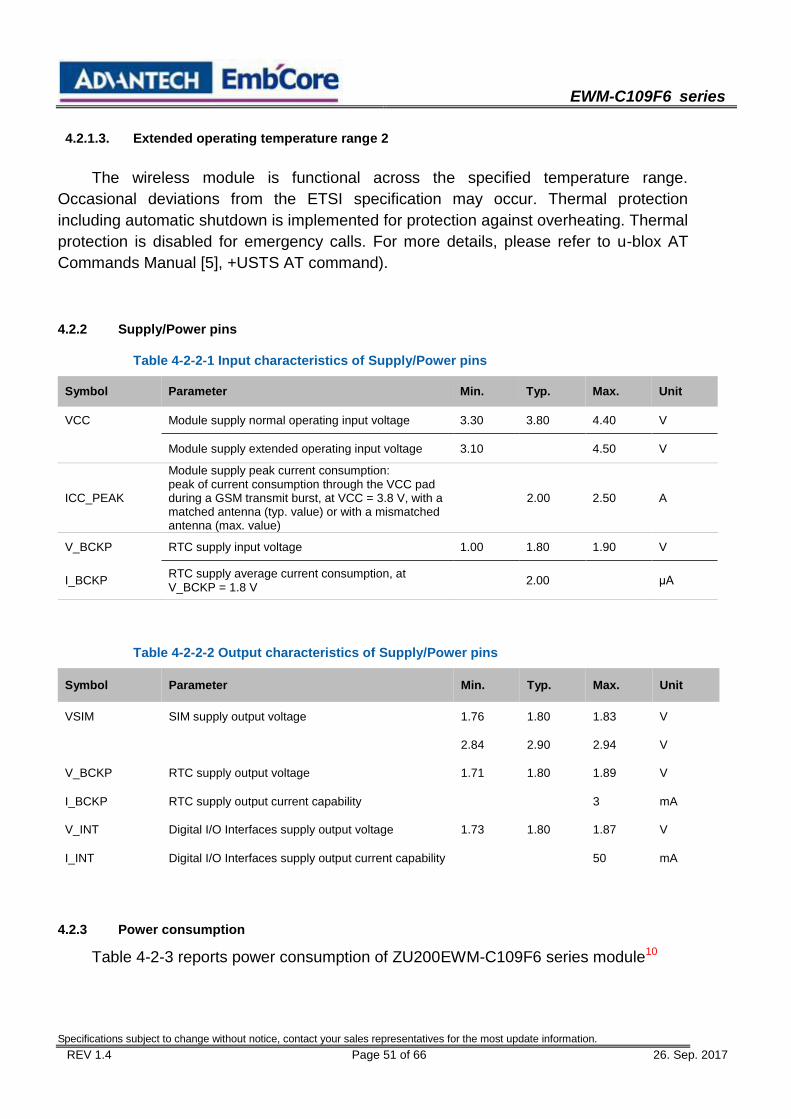
EWM-C109F6 series
Specifications subject to change without notice, contact your sales representatives for the most update information.
REV 1.4 Page 51 of 66 26. Sep. 2017
4.2.1.3. Extended operating temperature range 2
The wireless module is functional across the specified temperature range.
Occasional deviations from the ETSI specification may occur. Thermal protection
including automatic shutdown is implemented for protection against overheating. Thermal
protection is disabled for emergency calls. For more details, please refer to u-blox AT
Commands Manual [5], +USTS AT command).
4.2.2 Supply/Power pins
Table 4-2-2-1 Input characteristics of Supply/Power pins
Symbol Parameter Min. Typ. Max. Unit
VCC Module supply normal operating input voltage 3.30 3.80 4.40 V
Module supply extended operating input voltage 3.10 4.50 V
ICC_PEAK
Module supply peak current consumption: peak of current consumption through the VCC pad during a GSM transmit burst, at VCC = 3.8 V, with a matched antenna (typ. value) or with a mismatched antenna (max. value)
2.00 2.50 A
V_BCKP RTC supply input voltage 1.00 1.80 1.90 V
I_BCKP RTC supply average current consumption, at V_BCKP = 1.8 V
2.00 μA
Table 4-2-2-2 Output characteristics of Supply/Power pins
Symbol Parameter Min. Typ. Max. Unit
VSIM SIM supply output voltage 1.76 1.80 1.83 V
2.84 2.90 2.94 V
V_BCKP RTC supply output voltage 1.71 1.80 1.89 V
I_BCKP RTC supply output current capability 3 mA
V_INT Digital I/O Interfaces supply output voltage 1.73 1.80 1.87 V
I_INT Digital I/O Interfaces supply output current capability 50 mA
4.2.3 Power consumption
Table 4-2-3 reports power consumption of ZU200EWM-C109F6 series module10

EWM-C109F6 series
Specifications subject to change without notice, contact your sales representatives for the most update information.
REV 1.4 Page 52 of 66 26. Sep. 2017
Table 4-2-3 Power consumption
Mode Condition Power Consumption11
Power Off Mode Module is switched off by AT+CPWROFF < 60 μA
GSM/GPRS/EDGE Cyclic Idle/Active-Mode (Power Saving enabled by AT+UPSV)
Over all the supported 2G bands DRX = 512
USB interface not attached to a USB host
< 1.8 mA
Over all the supported 2G bands DRX = 5
12
USB interface in the suspend state < 2.2 mA
GSM Talk (Connected) Mode GSM 850 / E-GSM 900 bands Maximum Tx power (32.5 dBm typ.)
< 300 mA
DCS 1800 / PCS 1900 bands Maximum Tx power (29.5 dBm typ.)
< 210 mA
GPRS TBF (Connected) Mode GSM 850 / E-GSM 900 bands 4 Tx + 2 Rx slots (up to 85.6 kb/s UL, 42.8 kb/s DL) Maximum Tx power
< 600 mA
DCS 1800 / PCS 1900 bands 4 Tx + 2 Rx slots (up to 85.6 kb/s UL, 42.8 kb/s DL) Maximum Tx power
< 450 mA
EDGE TBF (Connected) Mode GSM 850 / E-GSM 900 bands 4 Tx + 2 Rx slots (up to 236.8 kb/s UL, 118.4 kb/s DL) Maximum Tx power
< 510 mA
DCS 1800 / PCS 1900 bands 4 Tx + 2 Rx slots (up to 236.8 kb/s UL, 118.4 kb/s DL) Maximum Tx power
< 460 mA
UMTS/HSxPA Cyclic Idle/Active-Mode (Power Saving enabled by AT+UPSV)
Over all the supported 3G bands DRX = 7
13 USB interface not attached to a USB
host
< 1.8 mA
Over all the supported 3G bands DRX = 7
13
USB interface in the suspend state < 2.2 mA
UMTS Talk (Connected) Mode Over all the supported 3G bands 12.2 kb/s UL, 12.2 kb/s DL Maximum Tx power
< 650 mA
HSDPA (Connected) Mode Over all the supported 3G bands 384 kb/s UL, 7.2 Mb/s DL Maximum Tx power
< 700 mA
HSUPA (Connected) Mode Over all the supported 3G bands 5.76 Mb/s UL, 384 kb/s DL Maximum Tx power
< 700 mA
HSPA (Connected) Mode Over all the supported 3G bands 5.76 Mb/s UL, 7.2 Mb/s DL Maximum Tx power
< 700 mA
10 It is assumed that no significant load is connected to any digital and analog pin except for antenna.
11 Maximum values for module average current consumption through the VCC pad in the listed
modes/conditions, at 25°C, with VCC = 3.8 V, with a matched antenna.
12 Module is registered with the network, with a paging period of 1177 ms (2G network DRX setting =
5), with 16 neighbour cells.
13 Module is registered with the network, with a paging period of 1280 ms (3G network DRX setting =
7), with 16 neighbour cells.

EWM-C109F6 series
Specifications subject to change without notice, contact your sales representatives for the most update information.
REV 1.4 Page 53 of 66 26. Sep. 2017
4.2.4 RF Performance
Table 4-2-4-1 Operating RF frequency bands
Parameter Min. Max. Unit Remarks
Frequency range GSM 850 Uplink 824 849 MHz Module transmit
Downlink 869 894 MHz Module receive
Frequency range E-GSM 900 Uplink 880 915 MHz Module transmit
Downlink 925 960 MHz Module receive
Frequency range DCS 1800 Uplink 1710 1785 MHz Module transmit
Downlink 1805 1880 MHz Module receive
Frequency range PCS 1900 Uplink 1850 1910 MHz Module transmit
Downlink 1930 1990 MHz Module receive
Frequency range UMTS 800 (band VI)
Uplink 830 840 MHz Module transmit
Downlink 875 885 MHz Module receive
Frequency range UMTS 850 (band V)
Uplink 824 849 MHz Module transmit
Downlink 869 894 MHz Module receive
Frequency range UMTS 900 (band VIII)
Uplink 880 915 MHz Module transmit
Downlink 925 960 MHz Module receive
Frequency range UMTS 1700 (band IV)
Uplink 1710 1755 MHz Module transmit
Downlink 2110 2155 MHz Module receive
Frequency range UMTS 1900 (band II)
Uplink 1850 1910 MHz Module transmit
Downlink 1930 1990 MHz Module receive
Frequency range UMTS 2100 (band I)
Uplink 1920 1980 MHz Module transmit
Downlink 2110 2170 MHz Module receive

EWM-C109F6 series
Specifications subject to change without notice, contact your sales representatives for the most update information.
REV 1.4 Page 54 of 66 26. Sep. 2017
Table 4-2-4-2 Receiver sensitivity performance
Parameter Min. Typ. Max. Unit Remarks
Receiver input sensitivity GSM 850
-102 -110 dBm Downlink RF level @ BER Class II < 2.4 %
Receiver input sensitivity E-GSM 900
-102 -110 dBm Downlink RF level @ BER Class II < 2.4 %
Receiver input sensitivity DCS 1800
-102 -109 dBm Downlink RF level @ BER Class II < 2.4 %
Receiver input sensitivity PCS 1900
-102 -109 dBm Downlink RF level @ BER Class II < 2.4 %
Receiver input sensitivity UMTS 800 (band VI)
-106 -111 dBm Downlink RF level for RMC @ BER < 0.1 %
Receiver input sensitivity UMTS 850 (band V)
-104 -112 dBm Downlink RF level for RMC @ BER < 0.1 %
Receiver input sensitivity UMTS 900 (band VIII)
-103 -111 dBm Downlink RF level for RMC @ BER < 0.1 %
Receiver input sensitivity UMTS 1700 (band IV)
-106 -111 dBm Downlink RF level for RMC @ BER < 0.1 %
Receiver input sensitivity UMTS 1900 (band II)
-104 -111 dBm Downlink RF level for RMC @ BER < 0.1 %
Receiver input sensitivity UMTS 2100 (band I)
-106 -111 dBm Downlink RF level for RMC @ BER < 0.1 %
Condition: 50 Ω source

EWM-C109F6 series
Specifications subject to change without notice, contact your sales representatives for the most update information.
REV 1.4 Page 55 of 66 26. Sep. 2017
Table 4-2-4-3 Transmitter maximum output power
Parameter Min. Typ. Max. Unit Remarks
Maximum output power GSM 850
31.0 32.5 35.0 dBm Uplink burst RF power for Single slot TCH at maximum output power control level (PCL5)
Maximum output power E-GSM 900
31.0 32.5 35.0 dBm Uplink burst RF power for Single slot TCH at maximum output power control level (PCL5)
Maximum output power DCS 1800
28.0 29.5 32.0 dBm Uplink burst RF power for Single slot TCH at maximum output power control level (PCL0)
Maximum output power PCS 1900
28.0 29.5 32.0 dBm Uplink burst RF power for Single slot TCH at maximum output power control level (PCL0)
Maximum output power UMTS 800 (Band VI
21.0 23.0 25.0 dBm Uplink continuous RF power for RMC at maximum power (continuous UP power control command)
Maximum output power UMTS 850 (Band V)
21.0 23.0 25.0 dBm Uplink continuous RF power for RMC at maximum power (continuous UP power control command)
Maximum output power UMTS 900 (Band VIII)
21.0 23.0 25.0 dBm Uplink continuous RF power for RMC at maximum power (continuous UP power control command)
Maximum output power UMTS 1700 (Band IV)
21.0 23.0 25.0 dBm Uplink continuous RF power for RMC at maximum power (continuous UP power control command)
Maximum output power UMTS 1900 (Band II)
21.0 23.0 25.0 dBm Uplink continuous RF power for RMC at maximum power (continuous UP power control command)
Maximum output power UMTS 2100 (Band I)
21.0 23.0 25.0 dBm Uplink continuous RF power for RMC at maximum power (continuous UP power control command)
Condition: 50 Ω output load
4.2.5 RESET_N pin
Table 4-2-5 RESET_N pin characteristics (ERS domain)
Pin Name Parameter Min. Typ. Max. Unit Remarks
RESET_N Internal supply for External Reset Input Signal
1.71 1.80 1.89 V RTC supply (V_BCKP)
L-level input -0.30 0.51 V
H-level input 1.32 2.01 V
L-level input current -180 μA
Pull-up resistance 10 kΩ Internal pull-up to RTC supply (V_BCKP)
RESET_N low time to perform a proper reset
50 ms
4.2.6 (U)SIM pins
The SIM pins are a dedicated interface to the (U)SIM chip card/IC. The electrical
characteristics fulfill regulatory specification requirements. The values in Table 4-2-6 are
for information only.

EWM-C109F6 series
Specifications subject to change without notice, contact your sales representatives for the most update information.
REV 1.4 Page 56 of 66 26. Sep. 2017
Table 4-2-6 (U)SIM pins characteristics (SIM domain)
Parameter Min. Typ. Max. Unit Remarks
Low-level input 0.00 0.35 V VSIM = 1.80 V
0.00 0.57 V VSIM = 2.90 V
High-level input 1.29 3.30 V VSIM = 1.80 V
2.07 3.30 V VSIM = 2.90 V
Low-level output 0.00 0.35 V VSIM = 1.80 V, Max value at IOL = +1.0 mA
0.00 0.35 V VSIM = 2.90 V, Max value at IOL = +1.0 mA
High-level output 1.26 1.80 V VSIM = 1.80 V, Min value at IOH = -1.0 mA
2.03 2.90 V VSIM = 2.90 V, Min value at IOH = -1.0 mA
Input/Output leakage current 0.7 μA 0.2V < VIN < 3.3V
Internal pull-up resistor on SIM_IO to VSIM
4.7 kΩ
Clock frequency on SIM_CLK 3.25 MHz
4.2.7 AC characteristics of digital audio interfaces pins
The 4-wire I2S digital audio interfaces can be configured in 4 different modes:
Normal I2S mode–Master mode
Normal I2S mode–Slave mode
PCM mode–Master mode
PCM mode–Slave mode
AC characteristics of the 4 different modes of the I2S digital audio interfaces are
reported as follows.

EWM-C109F6 series
Specifications subject to change without notice, contact your sales representatives for the most update information.
REV 1.4 Page 57 of 66 26. Sep. 2017

EWM-C109F6 series
Specifications subject to change without notice, contact your sales representatives for the most update information.
REV 1.4 Page 58 of 66 26. Sep. 2017

EWM-C109F6 series
Specifications subject to change without notice, contact your sales representatives for the most update information.
REV 1.4 Page 59 of 66 26. Sep. 2017

EWM-C109F6 series
Specifications subject to change without notice, contact your sales representatives for the most update information.
REV 1.4 Page 60 of 66 26. Sep. 2017

EWM-C109F6 series
Specifications subject to change without notice, contact your sales representatives for the most update information.
REV 1.4 Page 61 of 66 26. Sep. 2017

EWM-C109F6 series
Specifications subject to change without notice, contact your sales representatives for the most update information.
REV 1.4 Page 62 of 66 26. Sep. 2017
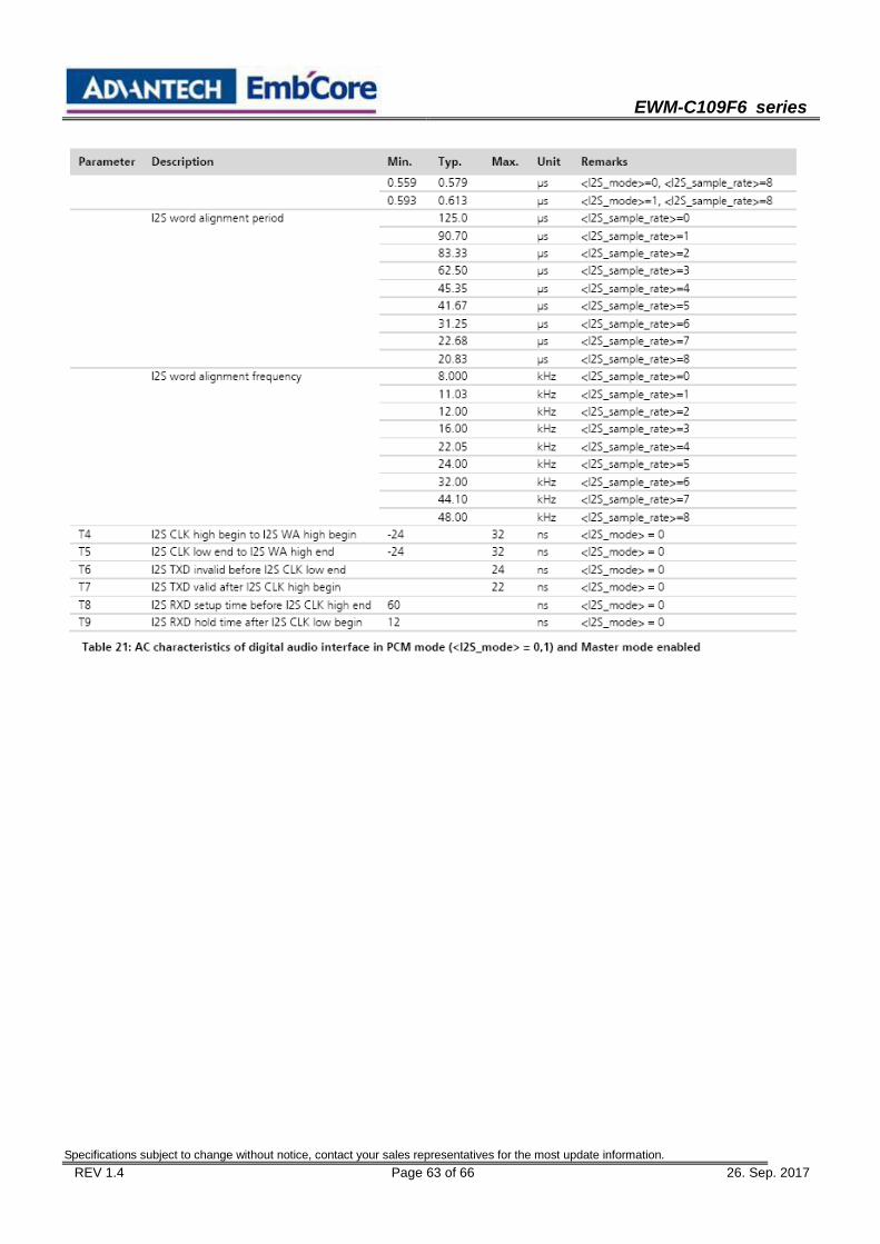
EWM-C109F6 series
Specifications subject to change without notice, contact your sales representatives for the most update information.
REV 1.4 Page 63 of 66 26. Sep. 2017

EWM-C109F6 series
Specifications subject to change without notice, contact your sales representatives for the most update information.
REV 1.4 Page 64 of 66 26. Sep. 2017

EWM-C109F6 series
Specifications subject to change without notice, contact your sales representatives for the most update information.
REV 1.4 Page 65 of 66 26. Sep. 2017

EWM-C109F6 series
Specifications subject to change without notice, contact your sales representatives for the most update information.
REV 1.4 Page 66 of 66 26. Sep. 2017
Appendix: Part Number Table
Product Advantech PN
3.75G UMTS/HSPA, w/ SIM Slot, 6-band WCDMA, Quad-band GSM/GPRS/EDGE, voice function
EWM-C109F601E
3.75G UMTS/HSPA, w/ SIM Slot, 6-band WCDMA, Quad-band GSM/GPRS/EDGE, voice function, with Hardware Standalone GPS Module
EWM-C109F6G1E