Embed Size (px)
Citation preview

i
Evaluation of organic perovskite photoconductors for x-ray imaging
detectors
Dhilippan Mamsapuram Panneerselvam
A Thesis
in
the Department
of
Electrical and Computer Engineering
Presented in Partial Fulfillment of the Requirement
for the Degree of Master of Applied Science at
Concordia University
Montréal, Québec, Canada
August 2017
© Dhilippan Mamsapuram Panneerselvam, 2017

ii
CONCORDIA UNIVERSITY
SCHOOL OF GRADUATE STUDIES
This is to certify that the thesis prepared
By: Dhilippan Mamsapuram Panneerselvam
Entitled: Evaluation of organic perovskite photoconductors for x-ray imaging detectors
and submitted in partial fulfillment of the requirements for the degree of
Master of Applied Science
Complies with the regulations of this university and meets the accepted standards with respect to
originality and quality.
Signed by the final examining committee:
________________________________________________ Chair
Dr. Robin Raut
________________________________________________ Examiner, External
Dr. Anjan Bhowmick (BCEE)
________________________________________________ Examiner
Dr. Steve Shih
________________________________________________ Supervisor
Dr. M. Z. Kabir
Approved by: ___________________________________________
Dr. W. E. Lynch, Chair
Department of Electrical and Computer Engineering
____________20_____ ___________________________________
Dr. Amir Asif, Dean
Faculty of Engineering and Computer
Science

iii
Abstract
Evaluation of organic perovskite photoconductors for x-ray imaging detectors
Dhilippan Mamsapuram Panneerselvam
Research over organic perovskites for light harvesting gained the momentum in past
decades. Due to the convenient low temperature and uniform deposition over large area these
materials are being tested for the vitality in various light harvesting devices such as in solar cells,
X-ray detectors, gamma photon captures etc., On meeting the expectation, the power conversion
efficiency in these devices peaked above 20% in around four years of research. But the underlying
physics in these materials remains a mystery particularly that which concerns the undesirable high
dark currents and photo gains when illuminated with X-ray for medical imaging.
In this thesis, the x-ray sensitivity of perovskite photoconductors under different detector operating
conditions has been identified. The primary mechanism that regulates the photocurrent and dark
current behavior of X-ray imagers based on organic perovskite photoconductors has been
identified. Energy level misalignments between different layers of X-ray imagers leading an
injective photo-gain has been investigated. The signal spreading due to trapping, k-fluorescence
generation and reabsorption, pixel aperture and primary charge interaction with photoconductor
has been accounted by calculating the theoretical MTF for different spatial frequency. These
imaging performances are also explored by calculating the theoretical Detective Quantum
Efficiency (DQE) at zero spatial frequency. Proceeding further, numerical investigation of organic
perovskite had also been accounted to visualize the electric field profiles along the thickness of
photoconductor. All possible recombination mechanisms and tr aps are included in the numerical
solution of continuity, trap, and Poisson's equations simultaneously. Sensitivity reduction due to
repeated exposure (Ghosting) has been investigated. A variation of electric field profile under
different exposure levels has been noticed. It becomes evident that significant deviations between
the analytical and numerical approaches were noticed under high exposure levels. This is due to
the significant variation of electric field profiles under very high exposures. The work in this thesis
identifies the important factors such as the need for appropriate blocking contacts for low dark
currents, improved carrier transport properties in perovskite films and proper energy level

iv
alignment between different layers of photodetector in order to make successful perovskite x-ray
detectors.

v
ACKNOWLEDGEMENT
My gratitude extends over this existence which made me a potential for the completion of
this thesis work. Principally, I would like to express my earnest gratitude to my supervisor Dr. M.
Z. Kabir for this motivation, encouragement, guidance and financial support throughout my thesis
work. I am also grateful to my parents who supported me mentally through their thought provoking
insights. I am also grateful to my colleagues Mr. Salman Moazzem Arnab and Mr. Kaveh
Rahbardar Mojaver for their innumerable friendly discussions. I would also like to extend my
gratitude to my colleague Ms. Nour Hijazi for help with COMSOL simulations. I am also grateful
to Mr. Md Mesbahus Saleheem for his encouragements, and friendly advice. Finally, I would like
to extend my gratitude to my lab mates named Ms. Sevin Samadi, Mr. Seyedamin Firouzeh, and
Ms. Fatemeh Ahmadi.

vi
With
meditative
awareness

vii
Table of contents
Abstract ............................................................................................................................................... iii
ACKNOWLEDGEMENT ................................................................................................................... v
Table of contents .................................................................................................................................vii
Table of Figures ................................................................................................................................... ix
List of tables ......................................................................................................................................... xi
List of Abbreviations ..........................................................................................................................xii
Chapter 1: Introduction .................................................................................................................... 1
1.1 X-rays ..................................................................................................................................... 1
1.2 X-ray imaging ........................................................................................................................ 1
1.2.1 Analog X-ray imaging ................................................................................................... 1
1.2.2 Digital X-ray imaging .................................................................................................... 2
1.2.3 Direct conversion X-ray detector .................................................................................. 2
1.2.4 Indirect conversion X-ray detector ............................................................................... 3
1.3 Image readout ........................................................................................................................ 4
1.4 Research Motivation ............................................................................................................. 5
1.4.1 Problem Identification ................................................................................................... 5
1.4.2 Excellency and perplexity of Perovskite – Present scenario ....................................... 6
1.5 Research objective ................................................................................................................. 7
1.6 Summary ................................................................................................................................ 7
Chapter 2: Literature review and theories....................................................................................... 8
2.1 Properties of Perovskite ........................................................................................................ 8
2.1.1 Composition and structure of Perovskite ..................................................................... 8
2.1.2 Band gap energy, Eg ...................................................................................................... 8
2.1.3 Charge carrier lifetime (τ) and mobility (µ) ................................................................. 9
2.2 Essential parameters defining an X-ray photodetector ..................................................... 10
2.2.1 X-ray Sensitivity .......................................................................................................... 10
2.2.2 Photo-gain .................................................................................................................... 11
2.2.3 Detector Structure ........................................................................................................ 12
2.2.4 Dark Current................................................................................................................. 15
2.2.5 Modulation transfer function....................................................................................... 15

viii
2.2.6 Detective Quantum Efficiency .................................................................................... 17
2.2.7 Ghosting ....................................................................................................................... 18
2.3 Properties of an ideal X-ray Photodetector ........................................................................ 19
2.4 Summary .............................................................................................................................. 20
Chapter 3: Analytical evaluation of organic perovskites ............................................................. 21
3.1 Abstract ................................................................................................................................ 21
3.2 Introduction .......................................................................................................................... 21
3.3 Characteristics of perovskite photoconductors .................................................................. 22
3.3.1 Attenuation Coefficient ............................................................................................... 23
3.3.2 X-ray sensitivity ........................................................................................................... 24
3.3.3 X-ray Photocurrent ...................................................................................................... 27
3.3.4 Detective Quantum efficiency .................................................................................... 30
3.3.5 Modulation transfer function....................................................................................... 32
3.4 Conclusions .......................................................................................................................... 35
Chapter 4: Numerical evaluation of organic perovskites ............................................................. 36
4.1 Equations depicting carrier transport ................................................................................. 36
4.2 Results and Discussion ........................................................................................................ 38
4.2.1 Numerical evaluation of perovskite based X-ray photodetector – Mammography
[26]…………………………………………………………………………………………..38
4.2.2 Numerical evaluation of perovskite based X-ray photodetectors – Chest
Radiography ................................................................................................................................ 44
4.3 Summary .............................................................................................................................. 50
Chapter 5: Conclusion, Contribution, and Future works ............................................................. 51
5.1 Conclusion ........................................................................................................................... 51
5.2 Contribution ......................................................................................................................... 52
5.3 Future Works ....................................................................................................................... 52
Chapter 6: Reference ...................................................................................................................... 54
ix
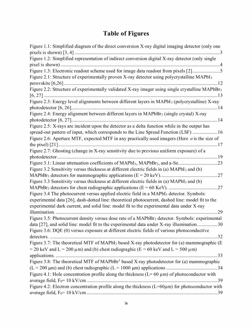
Table of Figures
Figure 1.1: Simplified diagram of the direct conversion X-ray digital imaging detector (only one
pixels is shown) [3, 4] .......................................................................................................................... 3
Figure 1.2: Simplified representation of indirect conversion digital X-ray detector (only single
pixel is shown) ...................................................................................................................................... 4
Figure 1.3: Electronic readout scheme used for image data readout from pixels [2] ....................... 5
Figure 2.1: Structure of experimentally proven X-ray detector using polycrystalline MAPbI3
perovskite [6,26] ................................................................................................................................. 12
Figure 2.2: Structure of experimentally validated X-ray imager using single crystalline MAPbBr3
[6, 27] .................................................................................................................................................. 13
Figure 2.3: Energy level alignments between different layers in MAPbI3 (polycrystalline) X-ray
photodetector [6, 26]........................................................................................................................... 14
Figure 2.4: Energy alignment between different layers in MAPbBr3 (single crystal) X-ray
photodetector [6, 27]........................................................................................................................... 14
Figure 2.5: X-rays are incident upon the detector as a delta function while in the output has
spread-out pattern of input, which corresponds to the Line Spread Function (LSF) ..................... 16
Figure 2.6: Aperture MTF, expected MTF in any practically used imagers (Here a is the size of
the pixel) [21] ...................................................................................................................................... 17
Figure 2.7: Ghosting (change in X-ray sensitivity due to previous uniform exposure) of a
photodetector ....................................................................................................................................... 19
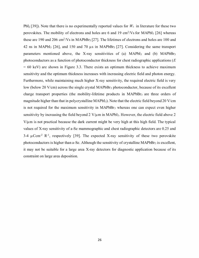
Figure 3.1: Linear attenuation coefficients of MAPbI3, MAPbBr3, and a-Se................................. 23
Figure 3.2 Sensitivity versus thickness at different electric fields in (a) MAPbI3 and (b)
MAPbBr3 detectors for mammographic applications (E = 20 keV)................................................ 27
Figure 3.3 Sensitivity versus thickness at different electric fields in (a) MAPbI3 and (b)
MAPbBr3 detectors for chest radiographic applications (E = 60 KeV). ......................................... 27
Figure 3.4 The photocurrent versus applied electric field in a MAPbI3 detector. Symbols:
experimental data [26], dash-dotted line: theoretical photocurrent, dashed line: model fit to the
experimental dark current, and solid line: model fit to the experimental data under X-ray
illumination. ........................................................................................................................................ 29
Figure 3.5: Photocurrent density versus dose rate of a MAPbBr3 detector. Symbols: experimental
data [27], and solid line: model fit to the experimental data under X-ray illumination. ................ 30
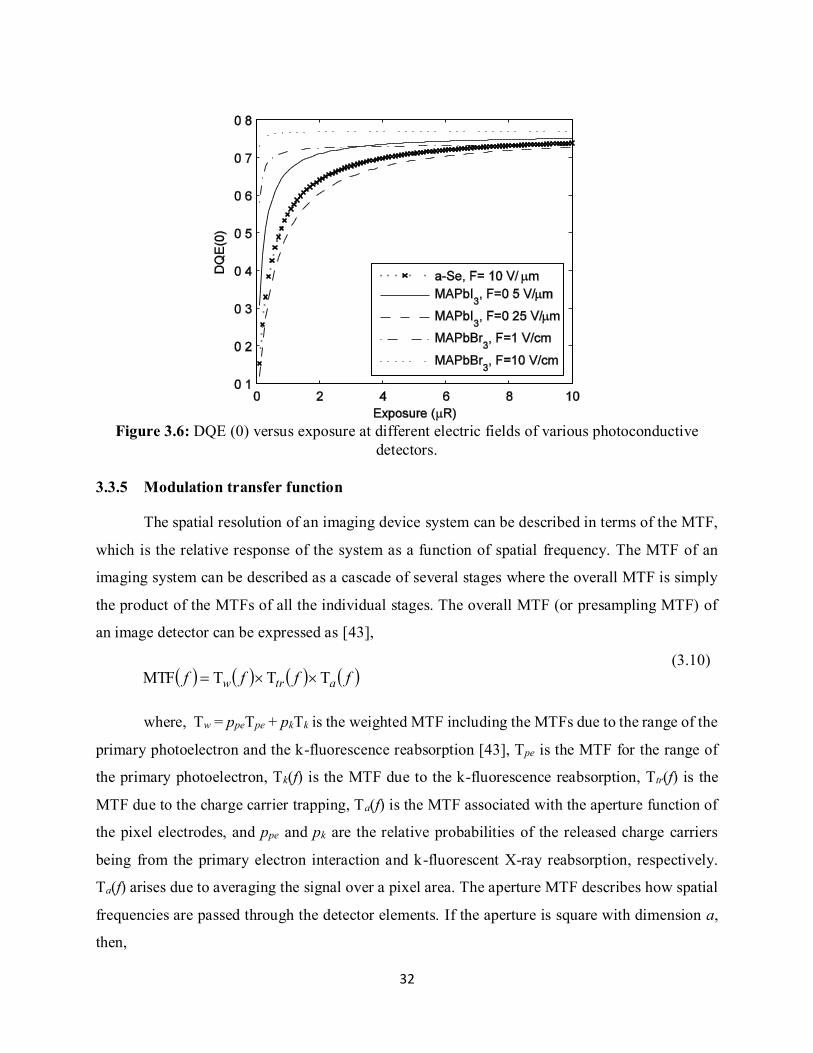
Figure 3.6: DQE (0) versus exposure at different electric fields of various photoconductive
detectors. ............................................................................................................................................. 32
Figure 3.7: The theoretical MTF of MAPbI3 based X-ray photodetector for (a) mammographic (E
= 20 keV and L = 200 m) and (b) chest radiograghic (E = 60 keV and L = 500 m)
applications. ........................................................................................................................................ 33
Figure 3.8: The theoretical MTF of MAPbBr3 based X-ray photodetector for (a) mammographic
(L = 200 µm) and (b) chest radiographic (L = 1000 µm) applications ........................................... 34
Figure 4.1: Hole concentration profile along the thickness (L= 60 µm) of photoconductor with
average field, F0= 10 kV/cm .............................................................................................................. 39
Figure 4.2: Electron concentration profile along the thickness (L=60µm) for photoconductor with
average field, F0= 10 kV/cm .............................................................................................................. 39
x
Figure 4.3: Distribution of trapped hole concentration across the thickness (L=60µm) of
photoconductor at the end of exposure time with average field, F0= 10 kV/cm ............................ 40
Figure 4.4: Distribution of trapped electron concentration across the thickness (L=60µm) of
photoconductor at the end of exposure time with initial field, F0= 10 kV/cm................................ 41
Figure 4.5: Photocurrent density vs time for L=60µm with average electric field, F0= 10 kV/cm
.............................................................................................................................................................. 42
Figure 4.6: Variation of photocurrent with respect to electric Field (E= 8 keV, L=60 µm) .......... 43
Figure 4.7: Electric Field profile across the thickness of the detector for various exposure levels
at the end of exposure time (E= 8 keV, F0= 10 kV/cm) ................................................................... 43
Figure 4.8: Hole concentration along the thickness of detector (L=500 µm) for chest radiography
application with average field, F0= 1 V/µm ...................................................................................... 44
Figure 4.9: Electron concentration along the thickness of detector (L=500µm) for chest
radiography application with average field, F0= 1 V/µm ................................................................. 45
Figure 4.10: Distribution of trapped hole concentration across the thickness (L=500µm) of
photoconductor at the end of exposure time with average field, F0= 1 V/µm ................................ 45
Figure 4.11: Distribution of trapped electron concentration across the thickness (L=500µm) of
photoconductor at the end of exposure time with average field, F0= 1 V/µm ................................ 46
Figure 4.12: Variation of sensitivity versus photoconductor thickness MAPbI3 ........................... 46
Figure 4.13: Electric field profile along the thickness of detector for various exposure levels (E=
60 keV, F0= 1 V/µm) .......................................................................................................................... 47
Figure 4.14: Ghosting characteristics of MAPbI3 X-ray photodetector (E=60keV) ...................... 48
Figure 4.15: Dose vs charge density in MAPbI3 x-ray detector. Experimental data were extracted
from [48] (E= 42 keV, F0= 0.2 V/µm, L= 0.8 mm).......................................................................... 49
Figure 4.16: Electric field profile along the thickness of photodetector corresponding to Figure
4.15 ...................................................................................................................................................... 50

xi
List of tables
Table 2.1: Comparison of band gap energy (Eg) of various organic perovskite materials which
are in the present state of art in optoelectronic research [8, 10] ........................................................ 9
Table 2.2: Comparison of charge carrier mobility and lifetime in various organic perovskite
compounds [12] .................................................................................................................................. 10
Table 3.1: Comparison of device parameters of an X-ray imaging system between different
active layer [22, 26, 27, 46]................................................................................................................ 35
xii
List of Abbreviations
A/D Analog to Digital
AMA Active Matrix Array
FPD Flat Panel Detector
TFT Thin Film Transistor
Ag Silver
Au Gold
Gd2O2S Gadolinium oxysulfide
CsI Cesium iodide
CH3NH3PbI3 Methyl ammonium lead iodide
CH3NH3PbBr3 Methyl ammonium lead bromide
PEDOT: PSS Poly polystyrene sulfonate
PCBM Phenyl-C61-butyric acid methyl ester
ZnO Zinc oxide
VB Valance Band
CB Conduction Band
HOMO Highest Occupied Molecular Orbit
LUMO Lowest Unoccupied Molecular Orbit
DQE Detective Quantum Efficiency
MTF Modulation Transfer Function
NPS Noise Power Spectrum
LSF Line Spread Function

1
Chapter 1: Introduction
1.1 X-rays
The innovation of X-rays on 1895 by Wilhelm Röntgen marks a landmark for medical
diagnosis of internal organs. X-rays are electromagnetic waves which can be produced when
electrons in the inner shell of a heavy atom are knocked out influencing the other electron from
the outer shell to fill this space. This process initiates the formation of x-rays. The produced x-rays
have very short wavelength (~nm) correspondingly larger energy. The unit of X-ray exposure is
Roentgen (R) in CGS systems while it has a unit of Gray (Gy) on modern SI system. Exposure
establishes the ability of X-ray to ionize the air. X-rays are mainly used in imaging of internal
organs and luggage scans.
1.2 X-ray imaging
X-rays encounters different attenuation for different materials. This lays the basis of X-ray
imaging in medical diagnosis. Depending upon the attenuation encountered on different body
parts, it forms a gray image for tissues, white for bones, and complete black images are obtained
for air [1]. The X-ray imaging has also seen an evolution. As such there can be two different types
of X-ray imaging techniques as Analog imaging technique and Digital imaging technique.
1.2.1 Analog X-ray imaging
An analog X-ray medical imaging uses photographic plates to record the images. These
photographic plates require chemical treatments to develop the images for diagnosis. According
to this process, the patients have been positioned appropriately between the X-ray tube and
photographic plate and exposure to x-rays are made. After the exposure of radiations, the
photographic plates are removed for post processing to develop the images. This process is time-
consuming as an ample time span is necessary to develop the image from photographic plates.
Furthermore, the probability that an appropriate image can be developed from these techniques is
low as it requires careful chemical processing of the films in dark rooms [2].
2
1.2.2 Digital X-ray imaging
The limitations of the analog X-ray imaging have been overcome through the usage of digital
imaging techniques. Here the images are formed instantaneously through the usage of X-ray
detectors, modern computers and image processing schemes. Better-quality images of the internal
organs can be developed with minimum dose deposition on patients through this technique. In this
technique, an X-ray detector (solid state device), and Active Matrix Arrays (AMA) are used. The
AMA is a 2-dimensional arrangement of many pixels. Each Pixel consist of a storage capacitor,
A/D converters and thin film transistors A/D converters are essential for interpretation of the
analog signal that is formed in imagers, to digital information. Thin film transistor (TFT) is used
as a switch to transfer the stored information of the image in capacitor for data processing. The
photodetector in this method forms the basis for imaging. In photodetector, the attenuated x-rays
(attenuated from the patient body) are absorbed and electron-hole pairs are generated. These
electron-hole pairs constitute the data for the image. In recent days, the Flat Panel Detector (FPD)
constituting an integrated package of the photodetector, thin film transistor, and A/D converters
are conveniently made in an Active Matrix Array (AMA). Not all the photoconductor establishes
a state where the electron-hole pairs are production through the direct absorption of the x-ray
radiation. Based on the scheme used to produce electron-hole pairs the digital X-ray imagers are
classified as direct conversion detector and indirect conversion detector.
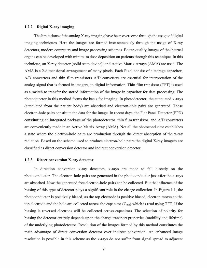
1.2.3 Direct conversion X-ray detector
In direction conversion x-ray detectors, x-rays are made to fall directly on the
photoconductor. The electron-hole pairs are generated in the photoconductor just after the x-rays
are absorbed. Now the generated free electron-hole pairs can be collected. But the influence of the
biasing of this type of detector plays a significant role in the charge collection. In Figure 1.1, the
photoconductor is positively biased, as the top electrode is positive biased, electron moves to the
top electrode and the hole are collected across the capacitor (Cmn) which is read using TFT. If the
biasing is reversed electrons will be collected across capacitors. The selection of polarity for
biasing the detector entirely depends upon the charge transport properties (mobility and lifetime)
of the underlying photodetector. Resolution of the images formed by this method constitutes the
main advantage of direct conversion detector over indirect conversion. An enhanced image
resolution is possible in this scheme as the x-rays do not suffer from signal spread to adjacent

3
pixel, multistep processes for the creation of electron-hole pair is avoided, and the addition of noise
in the signal is also limited due to direct formation of electron-hole pairs. Furthermore, the number
of layers required in the fabrication of the detector also less.
Figure 1.1: Simplified diagram of the direct conversion X-ray digital imaging detector (only one
pixels is shown) [3 ,4]
1.2.4 Indirect conversion X-ray detector
Indirect conversion is another method employed to mount the image from an object. Here
the scintillators play a major role in the conversion of incoming x-ray radiations to light photons
as shown in Figure 1.2. These generated light photons are then absorbed by the photoconductor on
the AMA. After absorption, the conventional process takes place in which the data (charge
collected) in the capacitors are read appropriately using the external peripheral circuitry.
Practically either gadolinium oxysulfide (Gd2O2S) or cesium iodide (CsI) is used as scintillators
for indirect conversion x-ray imagers. Normally indirect conversion x-ray imaging is not preferred

4
over direct conversion because the resolution of the images formed are poor and the light photon
generated in scintillators tend to spread toward the adjacent pixel and cause blur [2].
Figure 1.2: Simplified representation of indirect conversion digital X-ray detector (only single
pixel is shown)
1.3 Image readout
Figure 1.3, shown the image readout scheme for a group of pixels. Here Thin Film
Transistors (TFT) are used in the readout mechanism. All the TFT’s gate terminal are connected
for the trigger, while the data points are conveyed through the source terminal. When the gate
terminals in ‘m’ row is activated this will enable all the TFT in ‘m’ row and the data will be relayed
parallel to the multiplexer. This process continues to all the rows as m, m+1… Hence all the data
of images are read and relayed to a computer for image construction.

5
Figure 1.3: Electronic readout scheme used for image data readout from pixels [2]
1.4 Research Motivation
1.4.1 Problem Identification
With the present state of the art, most of the modern flat panel X-ray imaging systems are
dominated using a-Se (amorphous selenium) as a photoconductor because of its low dark current,
reasonable carrier transport properties and convenient deposition over a large area. But a-Se fails
to establish an ideal performance in many instances. Though the achievable sensitivity in the a-Se
based imager is significant and suitable for imaging, it has low conversion gain. Low conversion
gain corresponds to the inability of the material to produce sufficiently large electron-hole pairs
when X-rays are illuminated. Furthermore, the electron-hole pair creation energy (W±) has a strong
dependence on applied electric field (F) as,
nF
EBWW
)(0 (1.1)
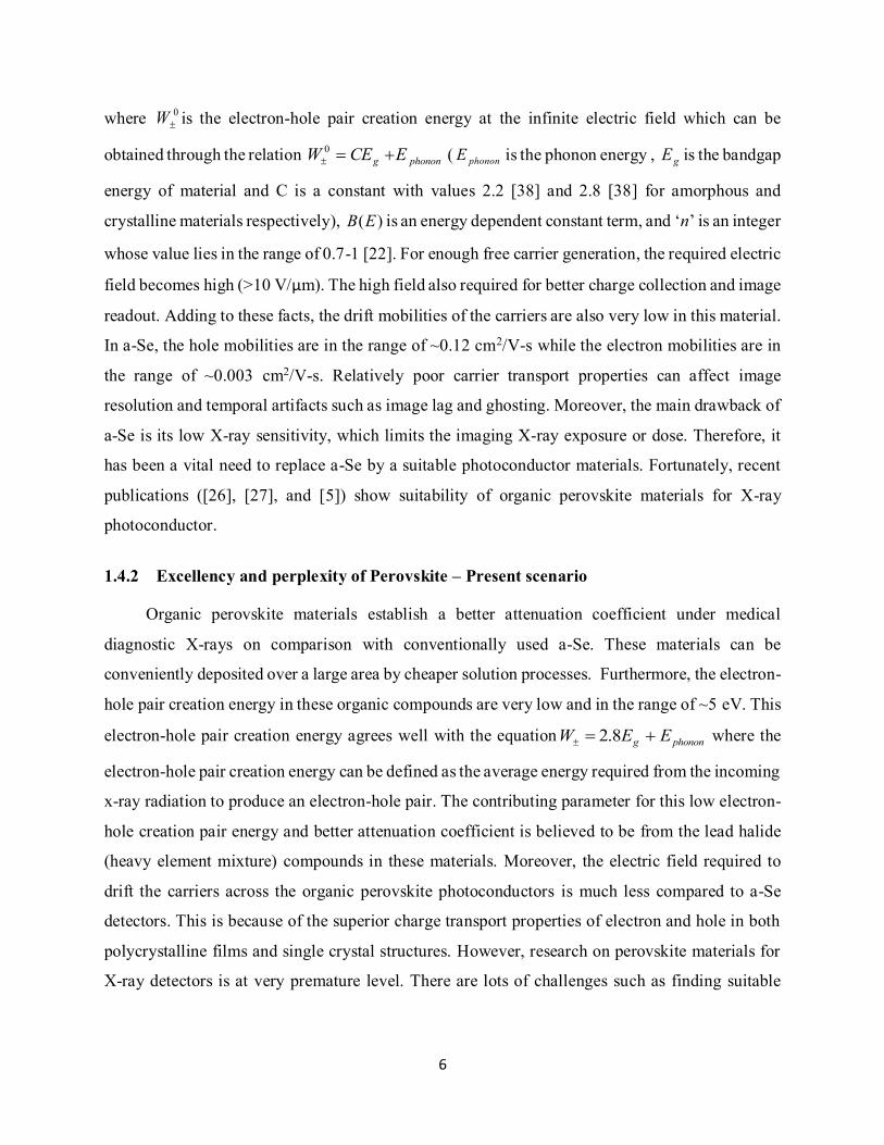
6
where 0
W is the electron-hole pair creation energy at the infinite electric field which can be
obtained through the relation phonong ECEW
0 ( phononE is the phonon energy , gE is the bandgap
energy of material and C is a constant with values 2.2 [38] and 2.8 [38] for amorphous and
crystalline materials respectively), )(EB is an energy dependent constant term, and ‘n’ is an integer
whose value lies in the range of 0.7-1 [22]. For enough free carrier generation, the required electric
field becomes high (>10 V/µm). The high field also required for better charge collection and image
readout. Adding to these facts, the drift mobilities of the carriers are also very low in this material.
In a-Se, the hole mobilities are in the range of ~0.12 cm2/V-s while the electron mobilities are in
the range of ~0.003 cm2/V-s. Relatively poor carrier transport properties can affect image
resolution and temporal artifacts such as image lag and ghosting. Moreover, the main drawback of
a-Se is its low X-ray sensitivity, which limits the imaging X-ray exposure or dose. Therefore, it
has been a vital need to replace a-Se by a suitable photoconductor materials. Fortunately, recent
publications ([26], [27], and [5]) show suitability of organic perovskite materials for X-ray
photoconductor.
1.4.2 Excellency and perplexity of Perovskite – Present scenario
Organic perovskite materials establish a better attenuation coefficient under medical
diagnostic X-rays on comparison with conventionally used a-Se. These materials can be
conveniently deposited over a large area by cheaper solution processes. Furthermore, the electron-
hole pair creation energy in these organic compounds are very low and in the range of ~5 eV. This
electron-hole pair creation energy agrees well with the equation phonong EEW 8.2 where the
electron-hole pair creation energy can be defined as the average energy required from the incoming
x-ray radiation to produce an electron-hole pair. The contributing parameter for this low electron-
hole creation pair energy and better attenuation coefficient is believed to be from the lead halide
(heavy element mixture) compounds in these materials. Moreover, the electric field required to
drift the carriers across the organic perovskite photoconductors is much less compared to a-Se
detectors. This is because of the superior charge transport properties of electron and hole in both
polycrystalline films and single crystal structures. However, research on perovskite materials for
X-ray detectors is at very premature level. There are lots of challenges such as finding suitable
7
detector structure for low dark current along with high sensitivity, resolution and better signal to
noise performance.
1.5 Research objective
The objective of this thesis is to evaluate and establish the scope of perovskite materials in X-
ray medical imaging. Hence this includes the research tasks as follows,
• Evaluating X-ray performances such as X-ray sensitivity, resolution, Detective Quantum
Efficiency (DQE) of perovskite photoconductors using analytical models.
• Developing a suitable numerical model to determine the limits of the established analytical
models and to examine the sensitivity reduction under repeated exposure.
• Investigating the origin of some unexpected detector phenomena such as excess carrier
injection and dark current.
1.6 Summary
In this chapter, the essential of X-ray imaging and image readout are discussed. Towards the
end, the research motivations are discussed along with my research objective. This thesis work is
divided into five chapters. The first chapter governed the initial introduction of X-ray imaging and
research motivation. The second chapter deals with the essential background theories of X-ray
imaging, metrics of an ideal X-ray photodetector along with recently resolved charged transport
properties of perovskite materials. Proceeding further, chapter three deals with the analytical
evaluation of perovskite materials for X-ray imaging. Numerical evaluation of organic perovskite
materials has been made in chapter four. Further scope of this material in X-ray imaging has been
highlighted in chapter five.

8
Chapter 2: Literature review and theories
In this chapter, the properties of organic perovskites, and essential parameters that qualify an
X-ray imaging detectors have been discussed. Moreover, vital conditions a photodetector must
possess to qualify for X-ray medical imaging has also been discussed.
2.1 Properties of Perovskite
2.1.1 Composition and structure of Perovskite
The first ever observed Perovskite compound was calcium titanate (CaTiO3) by German
mineralogist Gustav Rose on 1839 [6]. Over the evolution of time, research in the field of
optoelectronics concerns the usage of organic perovskite compounds [6], [7]. These organic
perovskite materials have the chemical composition ABX3, where A is the organic cation as
CH3NH3+ (methyl ammonium) or NH2CH3NH2
+ (formamidine), B is usually a divalent metal ion
either pb2+ or Sn2+, and X is the monovalent halogen atoms as Cl- or Br- or I-. The atomic
arrangement consists of the organic cation (A) occupying all the eight corners of the unit cell, the
divalent metal ion (B) is located at the body center of the unit cell, and the monovalent halogen
ions (X) are located at the face center of the unit cells.
Numerous possible perovskite materials can be formed by varying the A, B, and X elements in
perovskite composition 3ABX . But 333 PbXNHCH perovskite material, where orBrorClIX
has been of special interest in optoelectronic research because of their high carrier mobilities, low
charge recombination in bulk and low-temperature fabrication [8]. Recent review [9], highlighted
a sharp increase in the power conversion efficiency of these materials in less than a decade which
concludes that 333 PbINHCH is the best candidate for optoelectronic research.
2.1.2 Band gap energy, Eg
Band gap energy can be defined as the difference in energy levels between the top of the
valence band to the bottom of the conduction band. An insight on band gap, results in minimum
amount of energy required, from the exciting radiations, to excite an electron from the valence
band to the conduction band.

9
The band gap energy of complex three-dimensional perovskite structure )( 333 PbINHCH
observed though density function theory deduces an energy band gap of ~1.6 eV [10]. The
observed band gap of 333 PbINHCH is comparable with other organic perovskites, as given in
Table 2.1 below, by substituting halogen )(X atom.
Table 2.1: Comparison of band gap energy (Eg) of various organic perovskite materials
which are in the present state of art in optoelectronic research [8, 10]
Perovskite compound Band gap )( gE
333 PbINHCH ~1.6 eV
333 PbBrNHCH ~2.34 eV
333 PbClNHCH ~3.11 eV
2.1.3 Charge carrier lifetime (τ) and mobility (µ)
The charge carrier lifetime (τ) is defined as the average time a carrier take to recombine and
becomes unavailable for conduction. The mobility (µ) can be defined as velocity attained by the
carriers per unit electric field. The product of mobility and lifetime (µτ) determines the external
electric field required for efficient charge collection in each optoelectronic application.
Although a long range of charge transport has been reported for 333 PbINHCH perovskite
[11], with the present state of the art of these materials, the mobility and lifetime depend upon the
deposition techniques, nature of the film formed and the structure of the photodetectors.
Considering these phenomena’s, the mobility and lifetime of various organic perovskite films can
be summarized in
Table 2.2.

10
Table 2.2: Comparison of charge carrier mobility and lifetime in various organic perovskite
compounds [12]
Perovskite compound Mobility
(cm2V-1s-1)
Carrier lifetime
(µs)
333 PbINHCH
(Polycrystalline) ~1-10 ~0.01-1
333 PbINHCH
(Single crystal) ~24-105 ~0.5-1
333 PbBrNHCH
(Polycrystalline) ~30 ~0.05-0.16
333 PbBrNHCH
(Single crystal) ~24-115 ~0.3-1
2.2 Essential parameters defining an X-ray photodetector
2.2.1 X-ray Sensitivity
X-ray sensitivity can be defined as the charge collected per unit area per unit exposure of
radiations,
AX
QS
(2.1)
where Q is the collectible charge (C), A is the area of the photoconductor (cm2), and X is the
exposure level of incident radiation (R). Thus, the unit of X-ray sensitivity is C/cm2/R. The
exposure levels can also be conveniently defined in terms of SI unit as Gray, Gy (J/kg). 1 Roentgen
of exposure can be defined as,
1 R= 2.58×10⁻⁴ C/kg= 0.00876 J/kg= 8.76 mGy
for 3-cm1-airCmGyµ25 are imagersray -The experimentally obtained sensitivity of perovskite X
single crystal films. It is 3for MAPbBr 2-cm1-air80 µCmGypolycrystalline films and 3MAPbI
11
evident from these values of sensitivity that it is comparable with the values of sensitivity
obtained from conventionally used a-Se detectors.
2.2.2 Photo-gain
When the X-rays are absorbed on the photoconductor (perovskite) it results in the creation of
electron-hole pairs. These electron-hole pairs are separated and drifted to appropriately biased
contacts. The drifting carriers constitute the current both under illumination as well as in dark. But
recently many researchers [13,14, 15 and 16], have demonstrated that in photodetectors based on
perovskite there is an undesirable gain which is either due to injection or tunneling of carriers from
metal contacts.
One possible hypothesize about the origin of this gain is the presence of interfacial traps in
metal-semiconductor interfaces. The existence of these interfacial traps is argued due to the
presence of Pb2+ ions in perovskite films [17]. These ions at the interfaces create an ohmic interface
which favors the injection of carriers. One possible solution to this problem is to modulate the
concentration of Pb2+ ions during the preparation of perovskite films.
Another promising postulate for the origin of gain is the nature of films formed, by various
deposition techniques used in the fabrication process of photodetectors. Films deposited by spray
coating technique shows a superior gain. While the films deposited via spin coating shows a
negligible or no gain during the operation of the photodetector. These are due to the formation of
compact and dense films by spin coating while porous or less dense films by spray coating
technique [15, 16]. Remarkably the nature of films brings out a short circuit between different
layers. It is understood that a short circuit between glass (electrode) and photoconductor
principally constitute the gain (injection) during the operation of the photodetector [15, 16]. It is
also thought-provoking to note here that; the gain is a slow process and it establishes an onset time
for it to take place. Furthermore, the gain also depends upon the operating temperature of the
photodetector.
Figure 2.3 shows the energy band alignment of practically proven perovskite-based X-ray
imagers. From the above theories, it becomes evident that injection of carriers in this photodetector
takes place from metal (Ag) to photoconductor (Perovskite). Further theories of gain associated
12
with this perovskite-based x-ray detectors have been explained and the photocurrents are fitted
with experimental results in section 3.3.3.
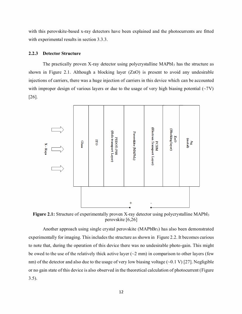
2.2.3 Detector Structure
The practically proven X-ray detector using polycrystalline MAPbI3 has the structure as
shown in Figure 2.1. Although a blocking layer (ZnO) is present to avoid any undesirable
injections of carriers, there was a huge injection of carriers in this device which can be accounted
with improper design of various layers or due to the usage of very high biasing potential (~7V)
[26].
Figure 2.1: Structure of experimentally proven X-ray detector using polycrystalline MAPbI3
perovskite [6,26]
Another approach using single crystal perovskite (MAPbBr3) has also been demonstrated
experimentally for imaging. This includes the structure as shown in Figure 2.2. It becomes curious
to note that, during the operation of this device there was no undesirable photo-gain. This might
be owed to the use of the relatively thick active layer (~2 mm) in comparison to other layers (few
nm) of the detector and also due to the usage of very low biasing voltage (~0.1 V) [27]. Negligible
or no gain state of this device is also observed in the theoretical calculation of photocurrent (Figure
3.5).

13
Figure 2.2: Structure of experimentally validated X-ray imager using single crystalline
MAPbBr3 [6, 27]

14
Figure 2.3: Energy level alignments between different layers in MAPbI3 (polycrystalline) X-ray
photodetector [6, 26]
Figure 2.4: Energy alignment between different layers in MAPbBr3 (single crystal) X-ray
photodetector [6, 18, 19, 20, 27]

15
The charge transport in these devices can be visualized using these energy alignment
diagrams. In Figure 2.3 and Figure 2.4, VB signifies Valence Band, CB signifies, Conduction
Band, LUMO signifies Lowest Unoccupied Molecular Orbit, and HOMO signifies Highest
Occupied Molecular Orbit.
2.2.4 Dark Current
An undesired current, after a biasing potential is applied across the photodetector without
illumination, is termed as dark current. Injection of carriers from the metal contacts constitutes a
chief mechanism for the origin of the dark current. An appropriate blocking contacts with larger
bandgap and interface matching layers at metal/semiconductor interface may reduce the dark
current. But the dark currents cannot be completely nullified due to some unbound charges. The
origin of these unbound charges is still a factor for debate, as it might arise due to thermal
generation of carriers from mid-bandgap of the semiconductors and it might also be associated
with some material properties used in different layers of the detectors. Dark currents in the range
of Femto to picoampere per mm2 are considered as an optimum level in X-ray imaging detectors.
An increase in the dark current above this range introduces image distortion or image blur in X-
ray imaging detectors. But X-ray imagers based on perovskite shows dark current in the range of
nano ampere. Hence investigating the mechanisms of the dark current has become vital in these
detectors.
2.2.5 Modulation transfer function
Resolving ability of an imaging detector under different spatial frequencies can be
conveniently expressed in terms of Modulation Transfer Function (MTF). It is the signal response
of the imaging system accounting photo-conducting material used and the dimensions of the
imaging system (pixel size). Superlatively, an MTF should reveal Fourier transform of the Point
Spread Function (PSF) with respect to the spatial frequency. But due to the complexity associated
with this transformation procedure a Fourier transform of the Line Spread Function (LSF) has been
agreed as an expedient norm for MTF description of an imaging system.

16
Figure 2.5: X-rays are incident upon the detector as a delta function while in the output has
spread-out pattern of input, which corresponds to the Line Spread Function (LSF)
The dependency of MTF on detector material and dimension (pixel dimension) establishes a
cascaded model for the calculation of a reliable MTF for imaging systems. Fundamentally the
resolution distortion of the image that arises due to the size of the pixel and the arrange of it (pixel
pitch). The MTF phenomena that arise out of it can be termed as aperture MTF (MTFap) which can
be qualified with a sinc function of a pixel width. Secondly, the MTF arising from K-fluorescence
reabsorption (MTFk) becomes significant. This undesirable and unpredictable image distortion
occurs due to the reabsorption of the secondary electron which has the energy corresponding to K-
edge of the photoconductor. It has always been a metric of measure to have a closer MTF due to
K-fluorescence with aperture MTF in imaging systems. Other parameters that contribute to the
signal response of an imaging system are the MTF due to the trapping levels (MTFtrap) in the
photoconductor, and the MTF results from the initial primary electron interaction (MTFpe). Thus,
the net MTF of imaging system is the product of individual MTF that is calculated due to individual
effects.
MTF= MTFpe× MTFk × MTFap × MTFap 2.2)
The MTF of an imaging system rolls down to zero at a spatial frequency ( f ) known as the
Nyquist frequency. This frequency is determined by pixel pitch (a) in the imaging detectors and
the Nyquist frequency can be expressed as )2/(1 afny . For the spatial frequencies above
Nyquist, the quality of the image formed will be distorted due to aliasing. Hence the aperture MTF
invariantly determines the ability of the detector for imaging under different spatial frequencies.

17
The expected MTF behavior of any practical imaging detector can be associated with the aperture
MTF as shown in Figure 2.6.
Figure 2.6: Aperture MTF, expected MTF in any practically used imagers (Here a is the size of
the pixel) [21]
2.2.6 Detective Quantum Efficiency
The imaging ability of any imaging system has been qualified with Detective Quantum
Efficiency (DQE). It defines the ability of the imaging system to transfer the signal with different
spatial frequencies from input to output with the minimal addition of noise. Hence DQE can be
conveniently defined as the ratio of SNRs at the output to input.
)(
)()(
2
2
fSNR
fSNRfDQE
in
out (2.3)
Ideally, an imaging system will possess a DQE equals unity. But in practice due to various
physical phenomena, the DQE rolls off from the ideal case. One primary reason is due to severe
variation in the spatial frequency of the object that must be imaged. Moreover, the deep trapped
charges and reabsorption of K-fluorescence lay down the law for DQE roll-off. The deeply trapped
charges in the semiconductor create a non-uniform charge collection and this, in turn, adds
additional noise in the system. Hence the DQE of the system starts to deviate from unity. Moving

18
on, the DQE reduction due to K-fluorescence reabsorption constitutes an important mechanism.
When X-rays strikes the photoconductor, it releases numerous primary electron but some
electrons, which corresponds to the K-edge energy, are reabsorbed and includes an undesired noise
during the imaging process. This mechanism is prone when photoconductor which has a K-edge
energy in the range of diagnostic medical imaging are used. Naturally a frequency dependent DQE
is preferred to explain the performance of the system. But for convenience and to avoid the
complexity of calculations the DQE at spatial frequency zero )0( f is chosen. DQE at zero
spatial frequency ))0((DQE signifies the decrease in the DQE performance of the imaging system
without considering the signal spread.
DQE has a dependency with MTF of the system. The MTF can be defined as the image blur
that is caused due to the scattering of image quanta. The relation between the DQE and MTF of
the system can be expressed as,
)(
)()0()(
2
fNPS
fMTFDQEfDQE
(2.4)
Where, )( fNPS is the noise power spectrum which can be approximated to one as spatial
frequency tends to zero.
2.2.7 Ghosting
Ghosting is defined as the change in X-ray sensitivity of the photoconductor due to the
previous exposure of radiations. Consider the Figure 2.7, where the X-rays are projected on a small
rectangle (left figure) then the X-rays are projected on the entire area. It becomes evident that it
forms a shadow image in the subsequent exposure. Thus, the ghosting reduces the pixel sensitivity
as well as it also worsens the image quality that has been formed. This phenomenon becomes a
significant threat when imaging is done in subsequent rapid frames (e.g.) fluoroscopy.

19
Figure 2.7: Ghosting (change in X-ray sensitivity due to previous uniform exposure) of a
photodetector
2.3 Properties of an ideal X-ray Photodetector
The essential properties that an ideal X-ray photodetector should pose when used in medical
imaging are as follows [22],
1. An ideal X-ray photodetector must have high quantum efficiency )( , this condition is
achievable when the penetration depth )( of incident X-ray does not exceed the thickness (L)
of the detectors )( L . That means, it should have a higher attenuation coefficient.
2. The electron-hole pair creation energy )( W must be low in order to create a sufficient number
of collectible electron-hole pairs per unit incident radiation.
3. Recombination in the bulk of photodetectors should be negligible.
4. Schubweg length, the mean distance a carrier travels by drifting before it becomes unavailable
for conduction, for both the holes and electron should be greater than the thickness of the
detector )( LF . This condition improves the charge transport property of the
photoconductor.
5. The most challenging condition that should be fulfilled by an imaging detector is to pose
extremely low dark current. An ideal X-ray imaging detector will hold zero dark current under
no illumination of X-rays. But in practice, the most acceptable level of dark current is in the

20
range of 10-1000 pA/cm2. These very low values of the dark currents are achievable by careful
engineering of a device structure to prevent any injection of carriers from the contacts.
6. Imaging detectors must be able to easily deposit uniformly over the entire Active Matrix Array
(AMA). Although excellent charge transport properties are achievable in many single crystal
imaging detectors, this condition prevents their commercialization as single crystal has the
constraint over large area deposition. Hence a better choice is the utilization of polycrystalline
or amorphous materials in X-ray imaging.
7. X-ray fatigue, deterioration of photodetector properties by repeated exposure to X-ray
radiation, should be negligible.
Perovskite materials (CH3NH3PbI3 and CH3NH3PbBr3) in this research work have been
critically evaluated by accounting most of the above-mentioned criteria for X-ray imaging.
2.4 Summary
Thus, in this chapter, the structural and electronics properties of different perovskite materials
are explained and compared with each other. Furthermore, the basic parameters used in
understanding an X-ray imaging detectors are briefed. Towards the conclusion, the qualificative
constraints for an X-ray imaging system are highlighted.

21
Chapter 3: Analytical evaluation of organic perovskites
The imaging performances of perovskite photoconductors are evaluated in this chapter. This
work has already been published [1].
3.1 Abstract
Enhancing the sensitivity of a direct conversion flat panel X-ray imaging detector with
minimum manufacturing cost has been a major dream for long decades. This criterion has been
recently addressed by the usage of MAPbX3 (MA is CH3NH3 and X is a halogen atom such as Cl,
I, or Br) perovskite in X-ray imaging detectors. Though MAPbI3 has shown large area deposition
capability and good X-ray sensitivity, it has to fulfill other criteria such as low dark current, high
spatial resolution and high signal to noise transfer capabilities. This paper evaluates the imaging
performances such as X-ray sensitivity, detective quantum efficiency (DQE) and modulation
transfer function (MTF) of organic perovskites (e.g., MAPbI3 and MAPbBr3) with a comparison
to amorphous selenium (a-Se). These perovskite materials have slightly higher linear attenuation
coefficients than a-Se and the expected X-ray sensitivity of these two perovskite photoconductors
is higher than a-Se. The mechanisms of the dark current and photocurrent gain in the MAPbI3
detector are also investigated. The MAPbI3 detector shows some photocurrent gain, which is due
to the enhanced electron injection under X-ray illumination. The expected theoretical zero spatial
frequency DQE of the MAPbI3 detectors is similar to that of a-Se while the MAPbBr3 detector
establishes a better DQE than a-Se. The expected MTF of the MAPbBr3 detectors is similar to that
of a-Se while the MAPbI3 shows worse resolution than a-Se. Based upon our theoretical
investigation, we believe that the organic perovskite can find its state of the art in near future if
rigorous research for improving the charge carrier transport properties and optimizing its detector
structure for low dark current were to be made.
3.2 Introduction
Mounting the image of the internal organs with minimal dose rate on the patient has been one
of the greatest challenges faced by recent medical imaging techniques. Amorphous selenium (a-
Se) is the most successful photoconductor for the direct conversion (the incident X-rays directly
[1] D. M. Panneerselvam and M. Z. Kabir, "Evaluation of organic perovskite photoconductors for direct conversion
X-ray imaging detectors", Journal of Materials Science: Materials in Electronics, vol. 28, no. 10, pp. 7083-7090,
2017.

22
generate electron and hole pairs, EHPs, in the photoconductor layer) flat-panel digital X-ray
detectors because of its low dark current, convenient deposition over large area, good charge
carrier transport properties (mobility and lifetime) and moderate X-ray sensitivity [23, 24, 25].
Recently, Yakunin et al. [26] reported that a thick layer (100 m) of polycrystalline
methylammonium lead iodide (poly-MAPbI3 where MA is CH3NH3) perovskite can be uniformly
deposited over a large area using a solution based synthesis technique without affecting the
underline Active Matrix Array (AMA) electronics. This material also shows a reasonable X-ray
absorption coefficient and its X-ray sensitivity is comparable to a-Se. Therefore, MAPbI3 can be
a potential candidate for large area X-ray detectors that leads to a new class of perovskite large-
area X-ray sensors. Although the reported 60 m thick detector [26] shows a reasonable level of
photocurrent for the X-ray fluence of 1.4×10⁷ photons mm-2 s-1, the dark current is almost half of
the photocurrent, which is not desirable for X-ray imaging. Moreover, the detectors show some
photocurrent gain, which will have some effects on the imaging performances. Therefore, it is vital
to investigate the origin of the photocurrent gain and high dark current and analyze the detector
performances by physics-based theoretical models.
In this paper, we examine the effects of X-ray interaction and charge transport properties on
the imaging performances such as X-ray sensitivity, detective quantum efficiency (DQE) and
modulation transfer function (MTF) of organic perovskites (e.g., MAPbI3 and MAPbBr3 [27]). We
also analyze the photocurrent characteristics with our physics-based theoretical model [28, 29] and
compare the theoretical results with the experimental data. We evaluate the quantity of signal that
could be lost due to traps or any recombination centers in the MAPbI3 and hence determine the
actual photocurrent gain. The mechanisms of the dark current and photocurrent gain in the
MAPbI3 are also studied. We find that the detector structure and the dark current mechanisms are
equally important as the charge carrier transport and X-ray absorption properties.
3.3 Characteristics of perovskite photoconductors
MAPbI3 is a direct bandgap semiconductor of bandgap energy of 1.6 eV and the relative
dielectric constant of 28. Its density is 4.3 g/cm3 [30]. The electron and hole mobilities in
polycrystalline films are 8 and 15 cm2/Vs, respectively [26]. The dark resistivity is 109 cm.
The effective masses of electrons and holes are 0.23m0 and 0.29m0 respectively [31], where m0 is
the free electron mass. The bandgap of MAPbBr3 is 2.3 eV [32], density is 3.8 g/cm3 and the

23
relative dielectric constant is 28 [33]. The electron and hole mobilities in crystalline MAPbBr3 are
190 and 206 cm2/Vs, respectively [27].
The basic detector structure consists of a photoconductor layer that is sandwiched between
two parallel plate electrodes. The top electrode (the radiation-receiving electrode) is biased with a
voltage V to establish an electric field F across the photoconductor layer and the charge is collected
from the bottom electrode. The biasing voltage can be positive if the holes have superior transport
properties (the product of mobility µ and carrier lifetime ) and negative for the superior transport
properties of electrons.
The effects of charge transport properties and attenuation coefficient of photoconductor
materials on the detector performances depend on the photoconductor thickness L and electric field
F through the following normalized parameters; the normalized attenuation depth (attenuation
depth/thickness) = 1/(L), the normalized electron schubweg (electron schubweg per unit
thickness) xe =eeF/L, and the normalized hole schubweg (hole schubweg per unit thickness) xh
= hhF/L. Here is the linear attenuation coefficient of the photoconductor, e(h) is the mobility,
and e(h) is the deep trapping time (lifetime) of electrons (holes). The schubweg (F) is the
distance a carrier drifts before it is deeply trapped and unavailable for conduction. The subscripts
h and e stand for holes and electrons respectively. Equivalently, xe and xh are the normalized carrier
lifetimes (carrier lifetimes per unit transit time) for electrons and holes, respectively.
3.3.1 Attenuation Coefficient
Figure 3.1: Linear attenuation coefficients of MAPbI3, MAPbBr3, and a-Se
24
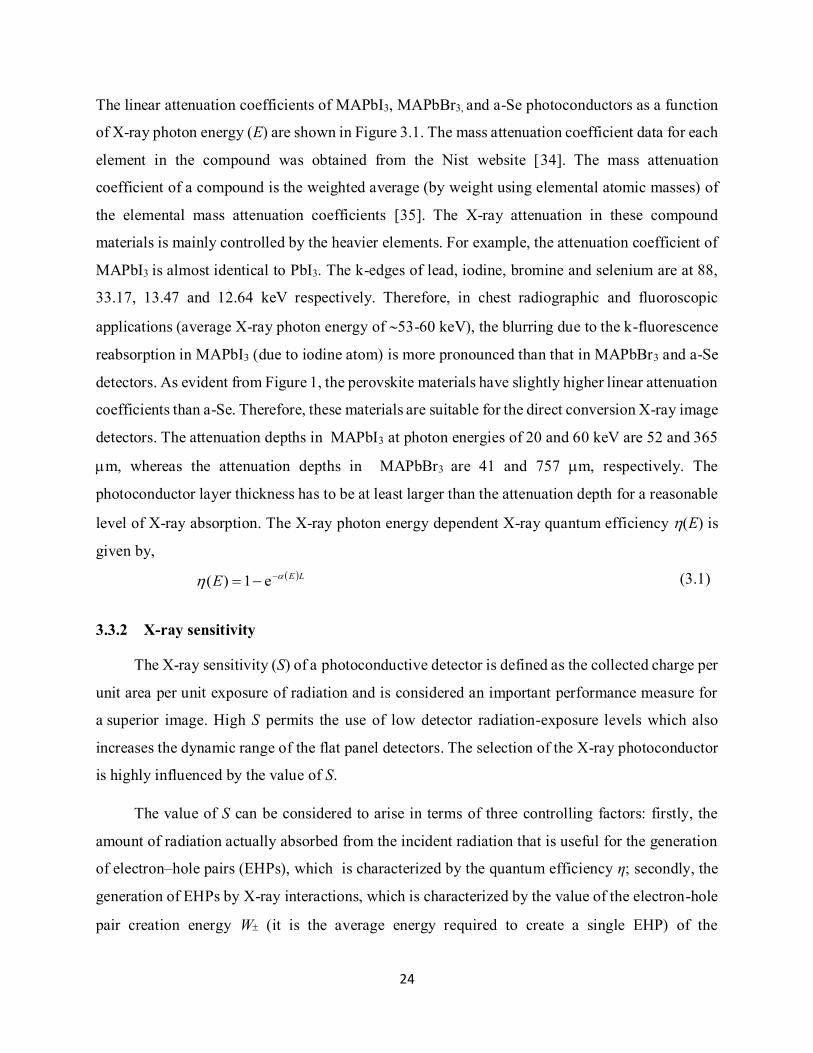
The linear attenuation coefficients of MAPbI3, MAPbBr3, and a-Se photoconductors as a function
of X-ray photon energy (E) are shown in Figure 3.1. The mass attenuation coefficient data for each
element in the compound was obtained from the Nist website [34]. The mass attenuation
coefficient of a compound is the weighted average (by weight using elemental atomic masses) of
the elemental mass attenuation coefficients [35]. The X-ray attenuation in these compound
materials is mainly controlled by the heavier elements. For example, the attenuation coefficient of
MAPbI3 is almost identical to PbI3. The k-edges of lead, iodine, bromine and selenium are at 88,
33.17, 13.47 and 12.64 keV respectively. Therefore, in chest radiographic and fluoroscopic
applications (average X-ray photon energy of 53-60 keV), the blurring due to the k-fluorescence
reabsorption in MAPbI3 (due to iodine atom) is more pronounced than that in MAPbBr3 and a-Se
detectors. As evident from Figure 1, the perovskite materials have slightly higher linear attenuation
coefficients than a-Se. Therefore, these materials are suitable for the direct conversion X-ray image
detectors. The attenuation depths in MAPbI3 at photon energies of 20 and 60 keV are 52 and 365
m, whereas the attenuation depths in MAPbBr3 are 41 and 757 m, respectively. The
photoconductor layer thickness has to be at least larger than the attenuation depth for a reasonable
level of X-ray absorption. The X-ray photon energy dependent X-ray quantum efficiency (E) is
given by,
LEE e1)( (3.1)
3.3.2 X-ray sensitivity
The X-ray sensitivity (S) of a photoconductive detector is defined as the collected charge per
unit area per unit exposure of radiation and is considered an important performance measure for
a superior image. High S permits the use of low detector radiation-exposure levels which also
increases the dynamic range of the flat panel detectors. The selection of the X-ray photoconductor
is highly influenced by the value of S.
The value of S can be considered to arise in terms of three controlling factors: firstly, the
amount of radiation actually absorbed from the incident radiation that is useful for the generation
of electron–hole pairs (EHPs), which is characterized by the quantum efficiency η; secondly, the
generation of EHPs by X-ray interactions, which is characterized by the value of the electron-hole
pair creation energy W (it is the average energy required to create a single EHP) of the

25
photoconductor and thirdly, how much of the X-ray generated charge is actually collected in the
external circuit. The later is characterized by the charge collection efficiency cc. If the top
electrode is positively biased, the cc for a monoenergetic X-ray beam is given by [28]
exhx
ee
hhcc
xx
xxE
1111
e11
11ee
1
11
(3.2)
It is assumed in equation (3.2) that the electric field is uniform across the photoconductor layer
under small signal operation, which is the case in diagnostic X-ray detectors [36]. If the bias
polarity is reversed, then xe and xh must be interchanged in equation (3.2). The X-ray Sensitivity S
of an X-ray imaging detector is conveniently normalized with respect to the maximum sensitivity
(S0) that would arise if all the incident radiation were absorbed and all the liberated carriers were
collected. The charge collection and absorption-limited normalized sensitivity s for a
monoenergetic X-ray beam is,
EESSEs cc 0 (3.3)
Assuming a sufficiently thick photoconductor layer so that the fluorescent X-rays (if any)
are reabsorbed within the photoconductor layer, the expression for S0 is given by, [37]
WES
airair
e1045.5 13
0 (3.4)
where e is the elementary charge, air and air are the energy absorption coefficient of air
and its density. If W± is expressed in eV, air/air is in cm2 g-1 and exposure (symbol not in equation
(3.4)) is in Roentgens, then S0 is in Ccm-2 R-1.
Figure 3.2 shows the X-ray sensitivity of (a) MAPbI3 and (b) MAPbBr3 photoconductors
as a function of photoconductor thickness at different electric fields and for mammographic
applications (The X-ray photon energy, E = 20 keV). The values of W in MAPbI3 and MAPbBr3
are taken as 5 and 6 eV as used in Refs. [26] & [27]. We believe that these are approximately the
theoretical values according to the Klein rule, 2.8Eg + Ephonon [38], where Ephonon is the phonon
energy. With Eg 1.6 eV and Ephonon < 0.5 eV, we would expect that W 5 eV. As mentioned in
section 3.3.1, since the attenuation coefficient of MAPbI3 is almost identical to PbI3 one would
expect that the value of W in MAPbI3 should be almost the same as in PbI3 (in fact, W 5 eV in
26
PbI2 [39]). Note that there is no experimentally reported values for W in literature for these two
perovskites. The mobility of electrons and holes are 6 and 19 cm2/Vs for MAPbI3 [26] whereas
these are 190 and 206 cm2/Vs in MAPbBr3 [27]. The lifetimes of electrons and holes are 100 and
42 ns in MAPbI3 [26], and 150 and 70 s in MAPbBr3 [27]. Considering the same transport
parameters mentioned above, the X-ray sensitivities of (a) MAPbI3 and (b) MAPbBr3
photoconductors as a function of photoconductor thickness for chest radiographic applications (E
= 60 keV) are shown in Figure 3.3. There exists an optimum thickness to achieve maximum
sensitivity and the optimum thickness increases with increasing electric field and photon energy.
Furthermore, while maintaining much higher X-ray sensitivity, the required electric field is very
low (below 20 V/cm) across the single crystal MAPbBr3 photoconductor, because of its excellent
charge transport properties (the mobility-lifetime products in MAPbBr3 are three orders of
magnitude higher than that in polycrystalline MAPbI3). Note that the electric field beyond 20 V/cm
is not required for the maximum sensitivity in MAPbBr3 whereas one can expect even higher
sensitivity by increasing the field beyond 2 V/m in MAPbI3. However, the electric field above 2
V/m is not practical because the dark current might be very high at this high field. The typical
values of X-ray sensitivity of a-Se mammographic and chest radiographic detectors are 0.25 and
3-4 Ccm-2 R-1, respectively [39]. The expected X-ray sensitivity of these two perovskite
photoconductors is higher than a-Se. Although the sensitivity of crystalline MAPbBr3 is excellent,
it may not be suitable for a large area X-ray detectors for diagnostic application because of its
constraint on large area deposition.

27
(a) (b)
Figure 3.2 Sensitivity versus thickness at different electric fields in (a) MAPbI3 and (b)
MAPbBr3 detectors for mammographic applications (E = 20 keV).
(a) (b)
Figure 3.3 Sensitivity versus thickness at different electric fields in (a) MAPbI3 and (b)
MAPbBr3 detectors for chest radiographic applications (E = 60 KeV).
3.3.3 X-ray Photocurrent
The duration of the X-ray exposure is usually much higher than the fastest carrier transit
time. The photocurrent due to an individual carrier transport (electron or hole) reaches almost a
steady value after its transit time. The photocurrent density due to hole transport under positive
bias is given by [29],

28
hhhhhh
hhhhhhh
h
TtFLFLL
FAe
TtFttLFtL
FAe
tJ
)]};/exp(1[)]exp(1{[
0)]};/exp(1)[exp()1)(/exp(1{[)(
(3.5)
where F
GA
hh
h
1
0 . The expression of G0 (in cm-3s-1) is given by [29],
exairair TW
XEG
13
0
1045.5
(3.6)
where t is the instantaneous time, Tex is the exposure time and X is the amount of
exposure/dose. If W± is expressed in eV, air/air is in cm2 g-1, is in cm-1, X is in Roentgens and
Tex in seconds, then G0 is in cm-3 s-1.
Similarly, the photocurrent density due to electron transport is [29],
eeeee
e
eeeeee
e
e
TtFLLFLL
FBe
TttLFFttL
FBe
tJ
)]};/exp(1)[exp()]exp(1{[
0)]};/exp(1)[exp()1()]/exp(1{[)(
(3.7)
Where F
GB
ee
e
1
0 .
The total photocurrent density, Jph = Jh + Je.
Figure 3.4 shows the current as a function of electric field in a MAPbI3 detector. The
symbols represent the experimental data, which are extracted from Ref. [26]. The dark
conductivity of this material is 1.410-9 Scm-1. Considering the contacts are ohmic-type, the
dark current (the current density = F) becomes almost three times larger than the measured
values. Therefore, the current is probably limited by the Schottky emission from the metal contacts.
The electron injection is more probable than the hole injection as discussed by Dong et al. [40].
The electron injection current density can be written as [24],
kTFeNJ e
eCinj
exp
(3.8)

29
where NC is the effective density of states in the conduction band, e is the effective barrier
height for the electron injection, k is the Boltzmann constant and T is the absolute temperature.
The dashed, dash-dotted and solid lines in Figure 3.4 represent the fitting of equation (3.8) with
experimental results under no illumination, the theoretical photocurrent and the model fit to the
experimental data under X-ray illumination, respectively. The photon energy E = 8 keV and
exposure rate is 2 R/s (2 mR per 1 ms), which corresponds to 1.4107 photons mm-2 s-1. The
electron-hole pair creation energy, W = 5 eV, L = 60 m, NC = 2.81018 cm-3, e = 6 cm2/Vs, h
= 19 cm2/Vs, e = 100 ns, and h = 42 ns. The fitted values of e under dark and X-ray illumination
are 0.57 and 0.52 eV, respectively. The difference between the dash-dotted line (theoretical
photocurrent) and the solid line represent the photocurrent gain, which is due to the enhanced
electron injection under X-ray illumination. We believe that the enhanced carrier injection occurs
due to the lack of appropriate blocking layers for the carrier injections from the metal electrodes.
Under dark condition, the energy barrier for electron injection from ZnO/Ag contact is larger. The
photogenerated holes are trapped near the PCBM/ZnO interface, which induces band bending,
reduces the barrier thickness and thus reduces the effective barrier height (see figure 1 of Ref.
[40]). The photocurrent gain is almost a linear function of the applied electric field.
Figure 3.4 The photocurrent versus applied electric field in a MAPbI3 detector. Symbols:
experimental data [26], dash-dotted line: theoretical photocurrent, dashed line: model fit to the
experimental dark current, and solid line: model fit to the experimental data under X-ray
illumination.

30
The photocurrent density as a function of dose rate in a MAPbBr3 detector is shown in
Figure 3.5. The experimental data were extracted from Ref. [27]. The electric field, F = 2 V/cm, E
= 22 keV, W = 5.3 eV, L = 2 mm, e = 190 cm2/Vs, h = 200 cm2/Vs, e = 150 s, and h = 70 s.
The detector shows a linear behavior with the dose rate and does not show any photocurrent gain.
Figure 3.5: Photocurrent density versus dose rate of a MAPbBr3 detector. Symbols:
experimental data [27], and solid line: model fit to the experimental data under X-ray
illumination.
3.3.4 Detective Quantum efficiency
The DQE measures the ability of the detector to transfer signal relative to noise from its
input to its output. Images are partially degraded by various sources of statistical fluctuations that
arise along the imaging chain. The relative increase in image noise due to an imaging system as
a function of spatial frequency f is expressed quantitatively by DQE(f) which represents the signal-
to-noise transfer efficiency for different frequencies of information in an image. The DQE(f) is
defined as
)(
)()(
2
2
fSNR
fSNRfDQE
in
out (3.9)
where SNRin and SNRout are the signal-to-noise ratios (SNR) at the input and output stages
of the image detector, respectively. DQE(f) is unity for an ideal detector. For simplicity, we are
31
often interested in measuring DQE(f = 0) of an imaging detector since it represents the signal
quality degradation due to the signal and noise transfer characteristics of the system without
considering signal spreading. Recently, Kabir et al. [41] have examined the effects of charge
carrier trapping and the K-fluorescent X-rays on the DQE of direct conversion X-ray detectors. In
this section, the DQE(0) model of Kabir et al. [41] is applied to a-Se, MAPbI3, and MAPbBr3
detectors for fluoroscopic applications to study and compare their DQE(0) performance.
Figure 3.6: DQE (0) versus exposure at different electric fields of various photoconductive
detectors.shows the DQE (0) as a function of X-ray exposure for a-Se, MAPbI3, and MAPbBr3
detectors for a 60-keV X-ray beam. The X-ray exposure (X) is varied from 0.1 μR to 10 μR, which
is the range of X-ray exposure for fluoroscopic applications. We assume that the pixel area,
A =200 μm ×200 μm, and the effective fill factor is 1.0 for all types of photoconductors. The
average E is 60 keV and the additive electronic noise (Ne) is assumed to be 2000 electrons per pixel
[42]. The following transport and operating parameters are used: for a-Se detectors, L =1000 μm,
F =10 V/μm, W±≈45 eV, μeτe =10−6 cm2/V and μhτh =10−5 cm2/V; for MAPbI3 detectors,
L =375 μm, W±=5 eV, μeτe =6×10⁻⁷ cm2/V and μhτh =810−7 cm2/V; and for MAPbBr3 detectors,
L =680 μm, W±=6 eV, μeτe =28.4×10⁻³ cm2/V and μhτh =14×10−3 cm2/V. The radiation-receiving
electrode is biased positively for all detectors. Δ ≈ 0.67 is for all detectors.
η = 1 − exp (− 1/Δ) ≈ 0.77 is the maximum achievable DQE(0) if all the liberated charges are
collected. The DQE(0) of the MAPbI3 detectors is similar to that of a-Se while the MAPbBr3
detector establishes a better DQE than a-Se.
32
Figure 3.6: DQE (0) versus exposure at different electric fields of various photoconductive
detectors.
3.3.5 Modulation transfer function
The spatial resolution of an imaging device system can be described in terms of the MTF,
which is the relative response of the system as a function of spatial frequency. The MTF of an
imaging system can be described as a cascade of several stages where the overall MTF is simply
the product of the MTFs of all the individual stages. The overall MTF (or presampling MTF) of
an image detector can be expressed as [43],
ffff atrw TTTMTF
(3.10)
where, Tw = ppeTpe + pkTk is the weighted MTF including the MTFs due to the range of the
primary photoelectron and the k-fluorescence reabsorption [43], Tpe is the MTF for the range of
the primary photoelectron, Tk(f) is the MTF due to the k-fluorescence reabsorption, Ttr(f) is the
MTF due to the charge carrier trapping, Ta(f) is the MTF associated with the aperture function of
the pixel electrodes, and ppe and pk are the relative probabilities of the released charge carriers
being from the primary electron interaction and k-fluorescent X-ray reabsorption, respectively.
Ta(f) arises due to averaging the signal over a pixel area. The aperture MTF describes how spatial
frequencies are passed through the detector elements. If the aperture is square with dimension a,
then,

33
af
afafcfa
sinsinT
(3.11)
The theoretical MTF of MAPbI3 based X-ray photodetector for mammographic (E = 20
keV and L = 200 m) and chest radiographic (E = 60 keV and L = 500 m) applications are shown
in Figure 3.7 (a) & (b). The pixel pitches for mammographic and chest radiographic detectors are
100 m and 200 m respectively. The analytical expressions for MTFpe, MTFk, and MTFtr are
taken from [28], [41] and [44], respectively. The mobility and lifetime of carriers in Figure 7 are
the same as in Figure 4 and the applied electric field F = 1 V/m. The loss of MTF due to k-
fluorescence reabsorption is absent in mammographic detectors because the average X-ray energy
(20 keV) is lower than the k-edge of iodine (33.17 keV). The MTFtr has a very significant effect
on the overall MTF because of poor charge carrier transport properties in polycrystalline MAPbI3.
The overall MTF of the mammographic detector is much better than that of chest radiographic
detectors. The overall MTF of mammographic detectors is mainly determined by the trapping
limited MTFtr. On the other hand, in chest radiographic detectors, both MTFk and MTFtr control
the overall MTF. The overall MTF deviates quite significantly from the aperture MTF.
(a) (b)
Figure 3.7: The theoretical MTF of MAPbI3 based X-ray photodetector for (a) mammographic
(E = 20 keV and L = 200 m) and (b) chest radiograghic (E = 60 keV and L = 500 m)
applications.
The theoretical MTF of MAPbBr3 based X-ray photodetector for mammographic (E = 20
keV and L = 200 m) and chest radiographic (E = 60 keV and L = 1000 m) applications are
shown in Figures 8 (a) & (b). The mobility and lifetime of carriers in Figure 3.8 are the same as in

34
Figure 3.5 and the applied electric field F = 10 V/cm. The overall MTF in mammographic detectors
is very close to the aperture MTF because of very good charge carrier transport properties and low
k-fluorescence X-ray photon energy of bromine (12.1 keV). The overall MTF of chest
radiographic detectors deviates quite significantly from the aperture MTF is mainly determined by
the trapping limited MTFtr.
(a) (b)
Figure 3.8: The theoretical MTF of MAPbBr3 based X-ray photodetector for (a) mammographic
(L = 200 µm) and (b) chest radiographic (L = 1000 µm) applications
The expected resolution of MAPbBr3 detectors is better than that of MAPbI3 because of
much better charge transport properties in MAPbBr3. The expected MTF of MAPbBr3 detectors is
similar to that of a-Se while MAPbI3 detectors show worse resolution than a-Se [45].
Thus the performance of perovskite based X- ray imaging system can be compared with
the conventionally used a- Se based detector as shown in Table 3.1 [22, 26, 27, 46],

35
Table 3.1: Comparison of device parameters of an X-ray imaging system between different
active layer [22, 26, 27, 46]
Sensitivity (µCcm-2R-1) Detective
Quantum
Efficiency
(DQE)
Resolution
(MTF)
Dark
Currents Mammography Chest
Radiology
Amorphous
Selenium
0.22- 0.24
(F= 10 V/µm)
2.1- 3.38
(F= 10 V/µm) Good Good
< 10 pA/mm2
(F<=20 V/µm)
MAPbI3
(Perovskite)
>2
(F= 2 V/µm)
>18
(F= 2 V/µm) Good Low ~ nA to µA
MAPbBr3
(Perovskite)
>3.2
(F= 20 V/cm)
>43
(F= 20 V/cm) Good Good ~ nA to µA
3.4 Conclusions
The effects of X-ray interaction and charge transport properties on the imaging
performances such as X-ray sensitivity, detective quantum efficiency (DQE) and modulation
transfer function (MTF) of organic perovskites (e.g., MAPbI3 and MAPbBr3) have been analyzed.
The MAPbI3 detector shows photocurrent gain, which is due to the enhanced electron injection
under X-ray illumination. These perovskite materials have slightly higher linear attenuation
coefficients than a-Se and the expected X-ray sensitivity of these two perovskite photoconductors
is higher than a-Se. The expected DQE(0) of the MAPbI3 detectors is similar to that of a-Se while
the MAPbBr3 detector establishes a better DQE than a-Se. The theoretical MTF of the MAPbBr3
detectors is similar to that of a-Se while the MAPbI3 shows worse resolution than a-Se. Owing to
these facts, we conclude if rigorous research were to be made for improving the charge carrier
transport properties and optimizing its detector structure (e.g., appropriate metal contacts and
blocking layers) for low dark current, organic perovskite has a very high potential to replace a-Se
in direct conversion X-ray detectors.

36
Chapter 4: Numerical evaluation of organic perovskites
The analytical models described in chapter Chapter 3: are valid for small signal case (which
is valid for single exposure in diagnostic medical imaging). However, under repeated exposures
the accumulated trapped charges in the detector becomes significant to make the electric field
profile non-uniform. In this case the analytical models are not valid and we need to develop a
numerical model for performance analysis. Thus, in this chapter, numerical solution of continuity
equations (solving for hole concentration p and electron concentration n) and trap rate equations
(solving for trapped hole concentration pt and trapped electron concentration nt) were performed
simultaneously using COMSOL Multiphysics. Furthermore, Poisson’s equation (solving for
electric potential V) was also coupled with continuity and trap equations. The sensitivity S of the
perovskite materials is calculated numerically by solving ordinary differential equations (ODE)
for charge density.
4.1 Equations depicting carrier transport
The continuity equation for hole and electron concentration in semiconducting materials can
be defined with respect to traps and recombination terms as [29 ,47],
tpr
p
p pnCpnCp
gpFxt
p
)(
(4.1)
npCpnCn
gnFxt
ntnr
n
n
)(
(4.2)
where g is the carrier generation rate, F is the electric field, np , is the mobility of holes and
electron (cm2V-1s-1), np , is the lifetime of holes and electron (s), tp and tn are the trapped hole and
electron concentration (cm-3) which are derived from the trap equations as [47],
p
tp
t pnpC
t
p
(4.3)
n
tn
t npnC
t
n
(4.4)

37
Cr is the bimolecular recombination coefficient between the free electrons and holes, Cp is
the capture coefficient between the free electron and trapped hole and Cn is the capture coefficient
between the free hole and trapped electron. The values of Cr, Cp, and Cn are calculated as [47],
)( np
r
eC
,
p
p
eC and
n
n
eC .
The generation rate of holes and electrons in cm-3s-1 can be expressed as [29, 47],
)exp()(
xWT
EEg
ex
o
(4.5)
where α is the linear attenuation coefficient (cm-1), E is the energy of the incident photon (eV),
Tex is the exposure time (s), W± is the electron-hole pair creation energy (eV), and ϕo is the
incident X-fluence (photons/cm2), expressed as,
EE
XE
air
air
o
))(
(
1045.5)(
13
(4.6)
where αair(E) is the linear attenuation coefficient of air dependent on the energy of the incident
photon (cm-1), ρair is the density of air, and X is the exposure of incident X-ray photon (R). The
instantaneous electric field F (x, t), )(dx
dVF across the photodetector thickness is calculated
dynamically using the Poisson’s equation as [47],
)(2
2
tt nnppe
x
V
(4.7)
From the carrier concentrations, the hole and electron current densities are calculated as [47],
L
ph FpdxL
etJ
0
)( (4.8)
L
ne FndxL
etJ
0
)( (4.9)
The total current density (A/cm2) is the summation of the hole and electron current densities as,

38
)()( tJtJJ eh (4.10)
Sensitivity, S (charge collected per unit area per unit exposure) has been calculated by
extracting the charge density (C) via the solution of ordinary differential equation (ODE) as,
0 Jdt
dC
(4.11)
Now the charge density is divided by the exposure X to obtain the sensitivity (S) of photoconductor
as,
X
CS
(4.12)
4.2 Results and Discussion
A positively biased photoconductor of thickness L is considered. Hence the boundary
conditions 0),0( tp and 0),( tLn are used for solving continuity equations. 0),0( VtV and
0),( tLV are used as boundary conditions for solving the Poisson’s equation. The initial
conditions are 0)0,()0,()0,()0,( xnxpxnxp tt [47]. Using the above-mentioned boundary
and initial conditions the continuity, trap and Poisson’s equations are solved simultaneously using
COMSOL Multiphysics 5.2a. The charge transport properties are maintained as discussed as in
section 3.3.
4.2.1 Numerical evaluation of perovskite based X-ray photodetector – Mammography [26]
For an X-ray incident photon energy of 8 keV on a perovskite photoconductor
(CH3NH3PbI3) with thickness (L) of 60 µm at F0(=V0/L)= 10 kV/cm the carrier distribution across
the thickness of the photoconductor is shown in Figure 4.1 and Figure 4.2. In this section 4.2.1, an
exposure level of 2 mR is maintained throughout the entire exposure time of 1 ms which
corresponds to 1.4×10⁷ photons/mm2/s.
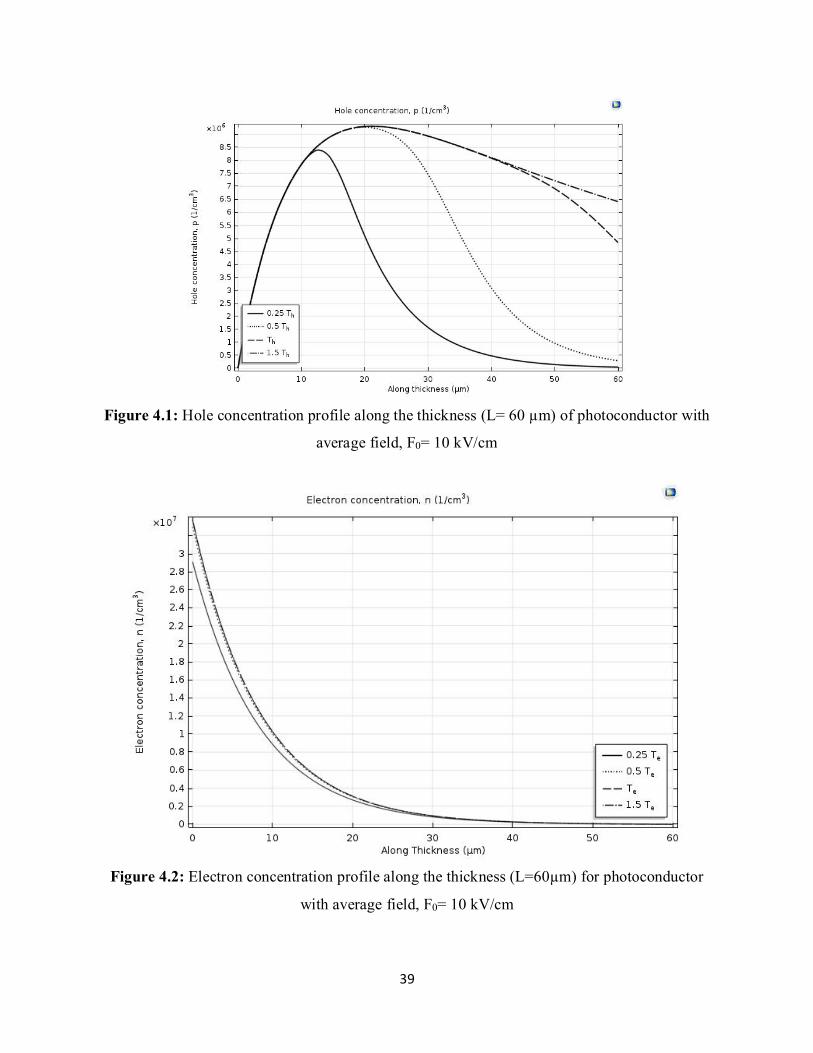
39
Figure 4.1: Hole concentration profile along the thickness (L= 60 µm) of photoconductor with
average field, F0= 10 kV/cm
Figure 4.2: Electron concentration profile along the thickness (L=60µm) for photoconductor
with average field, F0= 10 kV/cm

40
The simulations for charge carrier distributions, in Figure 4.1 and Figure 4.2, are carried
out for various transit times ehT , calculated through,
0,
,F
LT
eh
eh
(4.13)
The electron mostly resides near the top electrode because of exponential absorption and
carrier generation profile. It becomes evident that the steady state values are reached just after the
carrier transit times. The peak concentration of electron is higher compared with the hole
concentration because of the longer lifetime of an electron in perovskite polycrystalline films. The
calculated steady state current density for hole transport is 2.3197 nA/mm2 and for electron
transport is 0.45007 nA/mm2. Since the carrier generation profile is exponential, the generated
electrons quickly reach to the top electrode when the hole travel all the way down towards the
bottom electrode. As a result, the hole transport mostly contributes the photocurrent.
During these calculations, the MUMPS solver in COMSOL is optimized with a damping
factor of 1.45 and tolerance factor of 2.5 to avoid the stiffness during the numerical solution of
partial differential equations. The meshing levels are maintained at “Finer” (Maximum element
size of 0.12 µm) in user-defined semiconductor calibrations.
Figure 4.3: Distribution of trapped hole concentration across the thickness (L=60µm) of
photoconductor at the end of exposure time with average field, F0= 10 kV/cm

41
The trapped hole and electron ( tp and tn ) concentration for various lifetimes of electron
and holes, at the end of exposure (Tex), are shown in Figure 4.3 and Figure 4.4. From the
distribution profiles of trapped electron and hole, the peak electron trap concentration is slightly
higher than the hole trap concentration. However, electrons are mostly trapped near the top contact
whereas holes are trapped almost all over the detector thickness.
Figure 4.4: Distribution of trapped electron concentration across the thickness (L=60µm) of
photoconductor at the end of exposure time with initial field, F0= 10 kV/cm
With the obtained charge carrier distribution profiles, the photocurrent density (J) is calculated
using equations (4.8), (4.9), and (4.10). From Figure 4.5, the contribution of the hole current
density (Jh) to the total photocurrent density (J) is significant because of superior hole mobility
(µh= 19 cm2/V/s) in polycrystalline perovskite films. The photocurrent reaches a steady state value
after carrier transit time. The steady state photocurrent calculated by this method corresponds to
2.76977 nA/mm2.
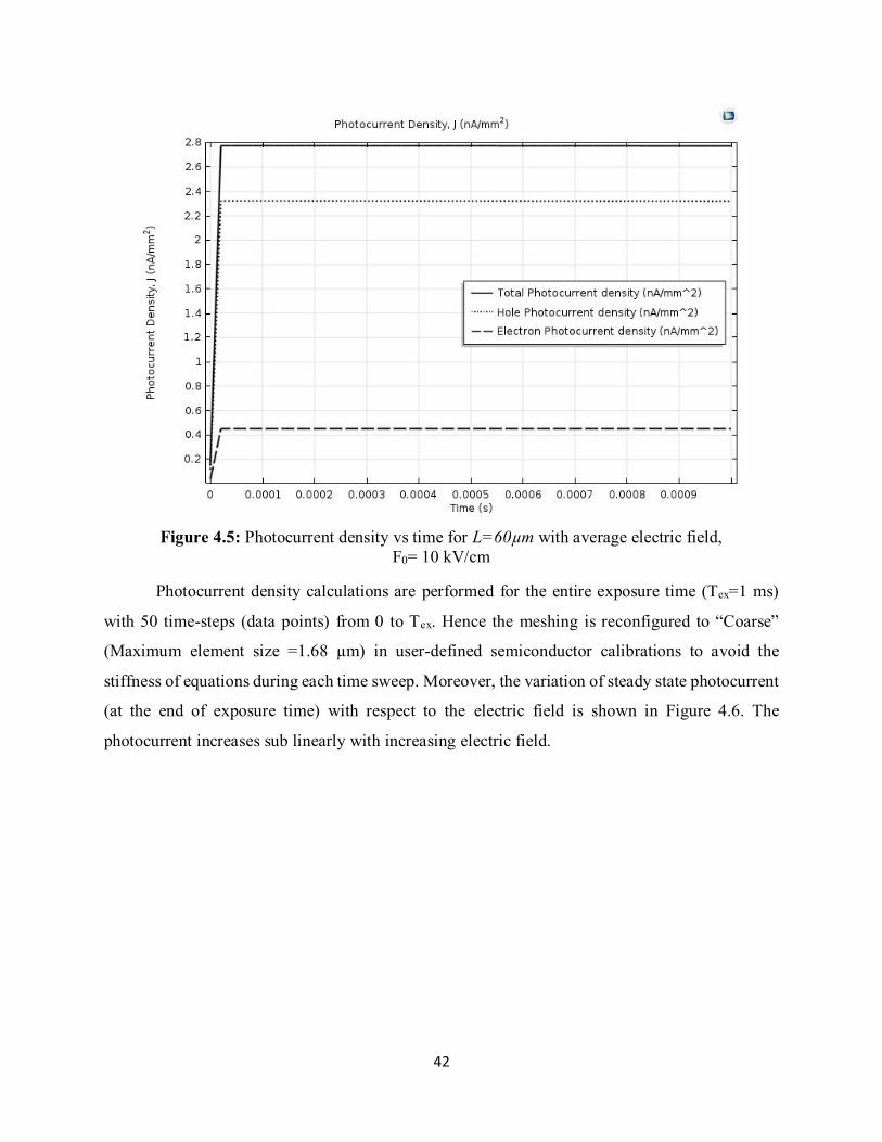
42
Figure 4.5: Photocurrent density vs time for L=60µm with average electric field,
F0= 10 kV/cm
Photocurrent density calculations are performed for the entire exposure time (Tex=1 ms)
with 50 time-steps (data points) from 0 to Tex. Hence the meshing is reconfigured to “Coarse”
(Maximum element size =1.68 µm) in user-defined semiconductor calibrations to avoid the
stiffness of equations during each time sweep. Moreover, the variation of steady state photocurrent
(at the end of exposure time) with respect to the electric field is shown in Figure 4.6. The
photocurrent increases sub linearly with increasing electric field.
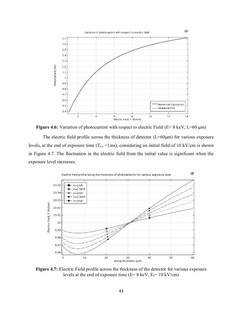
43
Figure 4.6: Variation of photocurrent with respect to electric Field (E= 8 keV, L=60 µm)
The electric field profile across the thickness of detector (L=60µm) for various exposure
levels, at the end of exposure time (Tex =1ms), considering an initial field of 10 kV/cm is shown
in Figure 4.7. The fluctuation in the electric field from the initial value is significant when the
exposure level increases.
Figure 4.7: Electric Field profile across the thickness of the detector for various exposure
levels at the end of exposure time (E= 8 keV, F0= 10 kV/cm)

44
4.2.2 Numerical evaluation of perovskite based X-ray photodetectors – Chest Radiography
In Chest radiography, X-rays are incident with an energy of 60 keV. The average exposure
level of 300 µR is maintained. The thickness of the perovskite detector (L) is optimized to 500 µm
over the conventionally used 1000 µm in a-Se based X-ray photodetectors. This optimization is
valid as it preserves the normalized attenuation depth )/1( L in perovskite detector over the
conventionally used a-Se X-ray detector.
The charge distributions across the thickness of photodetector are shown in Figure 4.8 and
Figure 4.9. From these figures, we can conclude that because of higher life time of electron, the
electron concentration is higher than hole concentration. The steady state value of hole current
density is 17.019 nA/mm2 and electron current density is 11.640 nA/mm2. The photocurrents due
to hole and electron transports are comparable because of nearly uniform carrier generation at
chest radiography detectors (higher x-ray photon energy). It is evident from the carrier profiles
that the steady state values are reached at the end of transit time for both electron and hole.
Figure 4.8: Hole concentration along the thickness of detector (L=500 µm) for chest
radiography application with average field, F0= 1 V/µm

45
Figure 4.9: Electron concentration along the thickness of detector (L=500µm) for chest
radiography application with average field, F0= 1 V/µm
Figure 4.10: Distribution of trapped hole concentration across the thickness (L=500µm) of
photoconductor at the end of exposure time with average field, F0= 1 V/µm
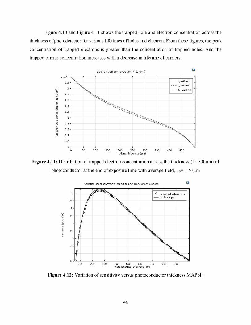
46
Figure 4.10 and Figure 4.11 shows the trapped hole and electron concentration across the
thickness of photodetector for various lifetimes of holes and electron. From these figures, the peak
concentration of trapped electrons is greater than the concentration of trapped holes. And the
trapped carrier concentration increases with a decrease in lifetime of carriers.
Figure 4.11: Distribution of trapped electron concentration across the thickness (L=500µm) of
photoconductor at the end of exposure time with average field, F0= 1 V/µm
Figure 4.12: Variation of sensitivity versus photoconductor thickness MAPbI3

47
Charge density is calculated from the current density through the solution of ordinary
differential equation (ODE) as in equation (4.11). And the sensitivity is calculated through the
formula (4.12).In Figure 4.12, the obtained sensitivity is compared with the standard analytical
model as described in [48]. From this comparison, it can be concluded that sensitivity obtained
through numerical calculation using COMSOL Multiphysics agrees well with the analytical
approach. There exists an optimum thickness that maximizes the sensitivity. This optimum
thickness increases with increasing mobility and lifetime.
Figure 4.13 shows the electric field profile variation along the thickness of the detector for
different exposure levels. The exposure levels cover the entire range used in chest radiography
from 30µR to 3000µR. It is evident that as the exposure level increases the electric field deviates
more from the initial value. Furthuremore, the average value of the field is the same as the initial
value of electric field.
Figure 4.13: Electric field profile along the thickness of detector for various exposure levels
(E= 60 keV, F0= 1 V/µm)

48
Figure 4.14: Ghosting characteristics of MAPbI3 X-ray photodetector (E=60keV)
Figure 4.14 shows the sensitivity of MAPbI3 photoconductor as a function of exposure for
two average electric field. The sensitivity decreases with increasing exposure and rate of reduction
decreases with exposure. As a result, the sensitivity may reach a plateau after a very high exposure.
The reduction of sensitivity after 1mGy of accumulated exposure is very significant (~53% at
F0=1V/µm, ~49% at F0=0.5V/µm). The non-uniform electric field and carrier recombination are
responsible for this reduction in sensitivity.
Recently, polycrystalline (MAPbI3) perovskite has been investigated with improved
fabrication techniques for its characteristics under varying dose [49]. The collected charge density
vs dose characteristic deviates from the expected linear behavior as shown in Figure 4.15. The
parameters used in Figure 4.15 and Figure 4.16; E=42keV, W±=4.5eV, L=0.8mm, µh= 0.7 cm2/V-
s, µe= 0.55 cm2/V-s, τh = τe = 350 µs, and Tex = 1s. Average incident energy (E) of 42 keV is
considered in numerical and analytical calculates which is extracted from the x-ray photon density
spectrum [49] with 2.5 mm Al filters and peak emission at 38 keV. It is evident from this fitting
that under high exposure levels (X>8mGy) neither the analytical nor numerical calculations catch
up with the experimental results. The analytical model shows a linear behavior because it does not

49
consider bimolecular recombination. Though the numerical model considers all kinds of
recombination and shows some nonlinear behavior, still it fails to follow the experimental trend.
Two more factor could be responsible such as (i) dose induced generation of new defects and (ii)
carrier density dependent free carrier generations.
Figure 4.15: Dose vs charge density in MAPbI3 x-ray detector. Experimental data were
extracted from [49] (E= 42 keV, F0= 0.2 V/µm, L= 0.8 mm)
The corresponding variation in the electric field along the thickness of photoconductor is shown
as in Figure 4.16.
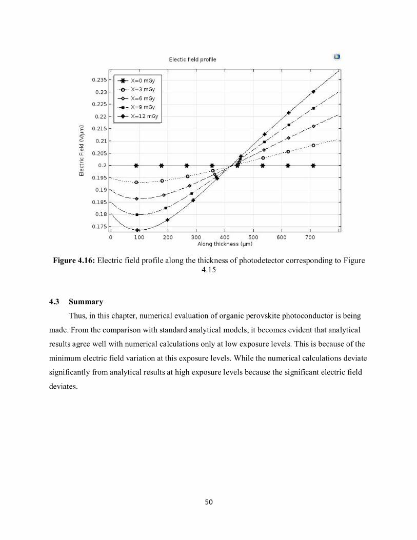
50
Figure 4.16: Electric field profile along the thickness of photodetector corresponding to Figure
4.15
4.3 Summary
Thus, in this chapter, numerical evaluation of organic perovskite photoconductor is being
made. From the comparison with standard analytical models, it becomes evident that analytical
results agree well with numerical calculations only at low exposure levels. This is because of the
minimum electric field variation at this exposure levels. While the numerical calculations deviate
significantly from analytical results at high exposure levels because the significant electric field
deviates.

51
Chapter 5: Conclusion, Contribution, and Future works
5.1 Conclusion
To sum it up, the standard analytical models of sensitivity, photocurrent, dark current
(injection limited), Detective Quantum Efficiency (DQE) at zero spatial frequency, and
Modulation Transfer Function (MTF) are applied to organic perovskite materials for establishing
the underlying mechanism and to assess the quality of signal loss during x-ray imaging. Based
upon these models the experimental values are fitted. Numerical investigations are also adopted in
this thesis work using COMSOL to exclude the assumption of a constant field in analytical
approaches. Furthermore, by numerical calculations, all possible recombination mechanism is
included. Hence, the electric field profile across the photoconductor thickness is plotted under
illumination of X-rays.
From these works, we conclude, an undesirable photo-gain arises in these materials which are
primarily governed by the injection of carriers from the contact terminals. Thus, a need for
appropriate blocking contacts with suitable material configurations between different layers of x-
ray detector is necessary. This different material configuration must include proper energy
alignment between different layer so that any possible charge injection (photo-gain) due to
tunneling and band bending can be avoided and the dark currents can be reduced drastically.
Although these perovskite materials have better linear attenuation coefficient and X-ray sensitivity
than of the a-Se detector, the theoretical MTF MAPbBr3 is like that of the a-Se based detector
while MAPbI3 shows worse resolutions. The Detective Quantum Efficiency (DQE) at zero spatial
frequency shows a similar result to that of a-Se. Proceeding further, from the ghosting (sensitivity
reduction) characteristics of MAPbI3, calculated by the numerical approach, it has been found that
under repeated exposure from 300 µR to 100 mR the sensitivity reduces ~53% at F0=1V/µm, ~49%
at F0=0.5V/µm from its initial value. Towards the end, under high exposure levels, the analytical
models do not agree well with the numerical approaches. Hence these analytical models are limited
to low exposure levels. This is due to significant variation of an electric field across the thickness
of photoconductor and carrier recombination at high exposure levels.

52
5.2 Contribution
The contribution of this thesis can be summarized below.
• Photo-gain mechanisms in polycrystalline MAPbI3 x-ray imagers are investigated
• Identified the need for structural optimization of x-ray detector with appropriate blocking
contacts for low dark current and any possible carrier injection
• Fitting of standard analytical models with experimental results are carried out
• Evaluated the carrier density profile, electric field profile and sensitivity under dynamic
conditions through numerical calculations using COMSOL.
The above works resulted in the following publications,
• D. M. Panneerselvam and M. Kabir, "Evaluation of organic perovskite photoconductors
for direct conversion X-ray imaging detectors", Journal of Materials Science: Materials in
Electronics, vol. 28, no. 10, pp. 7083-7090, 2017
• D. M. Panneerselvam and M. Z. Kabir, “Numerical evaluation of organic perovskite
photoconductors for X-ray image detectors”, The 18th Canadian Semiconductor Science
and Technology Conference, University of Waterloo, Ontario, Canada, August 20-24,
2017. (Accepted)
• D. M. Panneerselvam and M. Z. Kabir, “Performance evaluation of Perovskite
Photoconductors for direct conversion X-ray imaging detectors”, The 7th International
Conference on Optical, Optoelectronic and Photonic Materials and Applications,
Université de Montréal, Québec, Canada, June 13-17, 2016.
5.3 Future Works
The research on organic perovskite for light harvest has been increasing in recent years because
of the superior charge transport properties and low-temperature convenient fabrications. Because
of these inherited superiorities, the power conversion efficiency for light harvesting has peaked up
to more than 20% within four years of research. Yet there are unresolved queries when organic
perovskites are used in X-ray medical imaging. Few researchers tested X-ray sensitivity of their
photovoltaic structures and found quite encouraging result. However, a systemic study is vital
including the following issues

53
• A concrete photodetector structure concerning proper blocking contacts along with
appropriate energy alignment schemes needs to be developed to reduce the dark currents
• Convenient deposition scheme for large scale deposition of polycrystalline perovskite
without affecting the underlying Active Matrix Array (AMA) needs to be addressed
• Although ghosting on organic perovskite photoconductors has been resolved partially in
this thesis work, more general idea regarding the ghost recovery of images need to be
addressed for organic perovskite
• Detective Quantum Efficiency (DQE) variation with regards to different spatial frequency
needs to be addressed.
These ideas can be regarded as the direction for future work on organic perovskite for medical
X-ray imaging.

54
Chapter 6: Reference
[1] "RadiologyInfo.org", Radiologyinfo.org,2017. [Online]. Avalable
https://www.radiologyinfo.org/. [Accessed: 08- Jun- 2017].
[2] J. A. Rowlands and J. Yorkston, “Flat panel detectors for digital radiography” in Handbook
of Medical Imaging, vol. 1, J. Beutel, H. L. Kundel, and R. L. Van Metter, Ed. Washington:
SPIE, 2000, ch. 4.
[3] S. O. Kasap, M. Z. Kabir and J. Rowlands, "Recent advances in X-ray photoconductors for
direct conversion X-ray image detectors", Current Applied Physics, vol. 6, no. 3, pp. 288-
292, 2006.
[4] S. O. Kasap and J. A. Rowlands, “Direct-conversion flat-panel X-ray image detectors,” IEE
Proceedings: Circuits, Devices, and Systems, vol. 149, no. 2, pp. 85−96, Apr. 2002.
[5] W. Wei, Y. Zhang, Q. Xu, H. Wei, Y. Fang, Q. Wang, Y. Deng, T. Li, A. Gruverman, L.
Cao and J. Huang, "Monolithic integration of hybrid perovskite single crystals with
heterogenous substrate for highly sensitive X-ray imaging", Nature Photonics, vol. 11, no. 5,
pp. 315-321, 2017.
[6] Z. Song, S. Watthage, A. Phillips and M. Heben, "Pathways toward high-performance
perovskite solar cells: review of recent advances in organo-metal halide perovskites for
photovoltaic applications", Journal of Photonics for Energy, vol. 6, no. 2, p. 022001, 2016.
[7] M. Green, A. Ho-Baillie and H. Snaith, "The emergence of perovskite solar cells", Nature
Photonics, vol. 8, no. 7, pp. 506-514, 2014.
[8] A. Chilvery, A. Batra, B. Yang, K. Xiao, P. Guggilla, M. Aggarwal, R. Surabhi, R. Lal, J.
Currie and B. Penn, "Perovskites: transforming photovoltaics, a mini-review", Journal of
Photonics for Energy, vol. 5, no. 1, p. 057402, 2015.
[9] C. Zuo, H. Bolink, H. Han, J. Huang, D. Cahen and L. Ding, "Advances in Perovskite Solar
Cells", Advanced Science, vol. 3, no. 7, p. 1500324, 2016.

55
[10] T. Umebayashi, K. Asai, T. Kondo and A. Nakao, "Electronic structures of lead iodide
based low-dimensional crystals", Physical Review B, vol. 67, no. 15, 2003.
[11] G. Xing, N. Mathews, S. Sun, S. Lim, Y. Lam, M. Gratzel, S. Mhaisalkar and T. Sum,
"Long-Range Balanced Electron- and Hole-Transport Lengths in Organic-Inorganic
CH3NH3PbI3", Science, vol. 342, no. 6156, pp. 344-347, 2013.
[12] T. Brenner, D. Egger, L. Kronik, G. Hodes and D. Cahen, "Hybrid organic—inorganic
perovskites: low-cost semiconductors with intriguing charge-transport properties", Nature
Reviews Materials, p. 16011, 2016.
[13] K. Domanski, J. Correa-Baena, N. Mine, M. Nazeeruddin, A. Abate, M. Saliba, W. Tress,
A. Hagfeldt and M. Grätzel, "Not All That Glitters Is Gold: Metal-Migration-Induced
Degradation in Perovskite Solar Cells", ACS Nano, vol. 10, no. 6, pp. 6306-6314, 2016.
[14] K. Domanski, W. Tress, T. Moehl, M. Saliba, M. Nazeeruddin and M. Grätzel, "Working
Principles of Perovskite Photodetectors: Analyzing the Interplay Between Photoconductivity
and Voltage-Driven Energy-Level Alignment", Advanced Functional Materials, vol. 25, no.
44, pp. 6936-6947, 2015.
[15] H. Chen, N. Sakai, A. Jena, Y. Sanehira, M. Ikegami, K. Ho and T. Miyasaka, "A
Switchable High-Sensitivity Photodetecting and Photovoltaic Device with Perovskite
Absorber", The Journal of Physical Chemistry Letters, vol. 6, no. 9, pp. 1773-1779, 2015.
[16] T. Moehl, J. Im, Y. Lee, K. Domanski, F. Giordano, S. Zakeeruddin, M. Dar, L. Heiniger,
M. Nazeeruddin, N. Park and M. Grätzel, "Strong Photocurrent Amplification in Perovskite
Solar Cells with a Porous TiO2 Blocking Layer under Reverse Bias", The Journal of Physical
Chemistry Letters, vol. 5, no. 21, pp. 3931-3936, 2014.
[17] R. Dong, Y. Fang, J. Chae, J. Dai, Z. Xiao, Q. Dong, Y. Yuan, A. Centrone, X. Zeng and J.
Huang, "High-Gain and Low-Driving-Voltage Photodetectors Based on Organolead
Triiodide Perovskites", Advanced Materials, vol. 27, no. 11, pp. 1912-1918, 2015.
[18] J. Li, Z. Nie, H. Li, Y. Peng, Z. Wang, Z. Mai and W. Zheng, "A computational study of
tri-s-triazine-based molecules as ambipolar host materials for phosphorescent blue emitters:

56
effective geometric and electronic tuning", Journal of Materials Chemistry C, vol. 3, no. 19,
pp. 4859-4867, 2015.
[19] C. Kulshreshtha, G. Kim, R. Lampande, D. Huh, M. Chae and J. Kwon, "New interfacial
materials for rapid hole-extraction in organic photovoltaic cells", Journal of Materials
Chemistry A, vol. 1, no. 12, p. 4077, 2013.
[20] M. Waqas Alam, Z. Wang, S. Naka and H. Okada, "Mobility enhancement of top contact
pentacene based organic thin film transistor with bi-layer GeO/Au electrodes", Applied
Physics Letters, vol. 102, no. 6, p. 061105, 2013.
[21] D. C. Hunt, “Imaging performance of amorphous selenium flat-panel detector for digital
fluoroscopy,” SPIE Medical Imaging conference presentation, San Diego, (2003).
[22] M. Z. Kabir, S. O. Kasap, and J. A. Rowlands, “Photoconductors for X-ray Image Sensors”,
Springer Handbook of Electronic and photonic Materials, Springer Academic Publishers,
October 2006 (Chapter 48).
[23] S. Kasap, C. Koughia, J. Berashevich, R. Johanson and A. Reznik, "Charge transport in pure
and stabilized amorphous selenium: re-examination of the density of states distribution in the
mobility gap and the role of defects", Journal of Materials Science: Materials in Electronics,
vol. 26, no. 7, pp. 4644-4658, 2015.
[24] M. Z. Kabir, "Dark current mechanisms in amorphous selenium-based photoconductive
detectors: an overview and re-examination", Journal of Materials Science: Materials in
Electronics, vol. 26, no. 7, pp. 4659-4667, 2015.
[25] S. O. Kasap and J. Rowlands, "Review X-ray photoconductors and stabilized a-Se for direct
conversion digital flat-panel X-ray image-detectors", Journal of Materials Science: Materials
in Electronics, vol. 11, no. 3, pp. 179-198, 2000.
[26] S. Yakunin, M. Sytnyk, D. Kriegner, S. Shrestha, M. Richter, G. Matt, H. Azimi, C. Brabec,
J. Stangl, M. Kovalenko and W. Heiss, "Detection of X-ray photons by solution-processed
lead halide perovskites", Nature Photonics, vol. 9, no. 7, pp. 444-449, 2015.
57
[27] H. Wei, Y. Fang, P. Mulligan, W. Chuirazzi, H. Fang, C. Wang, B. Ecker, Y. Gao, M. Loi,
L. Cao and J. Huang, "Sensitive X-ray detectors made of methylammonium lead tribromide
perovskite single crystals", Nature Photonics, vol. 10, no. 5, pp. 333-339, 2016.
[28] M. Z. Kabir, "Effects of charge carrier trapping on polycrystalline PbO x-ray imaging
detectors", Journal of Applied Physics, vol. 104, no. 7, p. 074506, 2008.
[29] S. Siddiquee and M. Z. Kabir, "Modeling of photocurrent and lag signals in amorphous
selenium x-ray detectors", Journal of Vacuum Science & Technology A: Vacuum, Surfaces,
and Films, vol. 33, no. 4, p. 041514, 2015.
[30] T. Baikie, Y. Fang, J. Kadro, M. Schreyer, F. Wei, S. Mhaisalkar, M. Graetzel and T. White,
"Synthesis and crystal chemistry of the hybrid perovskite (CH3NH3)PbI3 for solid-state
sensitised solar cell applications", Journal of Materials Chemistry A, vol. 1, no. 18, p. 5628,
2013.
[31] G. Giorgi, J. Fujisawa, H. Segawa and K. Yamashita, "Small Photocarrier Effective Masses
Featuring Ambipolar Transport in Methylammonium Lead Iodide Perovskite: A Density
Functional Analysis", The Journal of Physical Chemistry Letters, vol. 4, no. 24, pp. 4213-
4216, 2013.
[32] E. Edri, S. Kirmayer, D. Cahen and G. Hodes, "High Open-Circuit Voltage Solar Cells
Based on Organic–Inorganic Lead Bromide Perovskite", The Journal of Physical Chemistry
Letters, vol. 4, no. 6, pp. 897-902, 2013.
[33] A. Poglitsch and D. Weber, "Dynamic disorder in methylammoniumtrihalogenoplumbates
(II) observed by millimeter‐wave spectroscopy", The Journal of Chemical Physics, vol. 87,
no. 11, pp. 6373-6378, 1987.
[34] "X-Ray and Gamma-Ray Data", NIST, 2017. [Online]. Available:
https://www.nist.gov/node/428981. [Accessed: 12- Mar- 2017].
[35] J. Beutel, H. L. Kundel and R. L. Van Metter (eds.) Handbook of Medical Imaging, (SPIE
Press, Washington, 2000), p. 31.
58
[36] M. Z. Kabir, E. Emelianova, V. Arkhipov, M. Yunus, S. O. Kasap and G. Adriaenssens,
"The effects of large signals on charge collection in radiation detectors: Application to
amorphous selenium detectors", Journal of Applied Physics, vol. 99, no. 12, p. 124501, 2006.
[37] S. O. Kasap, "X-ray sensitivity of photoconductors: application to stabilized a-Se", Journal
of Physics D: Applied Physics, vol. 33, no. 21, pp. 2853-2865, 2000.
[38] C. Klein, "Bandgap Dependence and Related Features of Radiation Ionization Energies in
Semiconductors", Journal of Applied Physics, vol. 39, no. 4, pp. 2029-2038, 1968.
[39] S. O. Kasap, M. Z. Kabir and J. Rowlands, "Recent advances in X-ray photoconductors for
direct conversion X-ray image detectors", Current Applied Physics, vol. 6, no. 3, pp. 288-
292, 2006.
[40] R. Dong, Y. Fang, J. Chae, J. Dai, Z. Xiao, Q. Dong, Y. Yuan, A. Centrone, X. Zeng and J.
Huang, "High-Gain and Low-Driving-Voltage Photodetectors Based on Organolead
Triiodide Perovskites", Advanced Materials, vol. 27, no. 11, pp. 1912-1918, 2015.
[41] M. Z. Kabir, M. W. Rahman, and W. Y Shen, “Modelling of DQE of direct conversion X-
ray imaging detectors incorporating charge carrier trapping and K-fluorescence,” IET
Circuits Devices and Systems, vol. 5, pp. 222-231, 2011.
[42] M. Z. Kabir and S. O. Kasap, "DQE of photoconductive x-ray image detectors: application
to a-Se", Journal of Physics D: Applied Physics, vol. 35, no. 21, pp. 2735-2743, 2002.
[43] W. Que and J. Rowlands, "X-ray imaging using amorphous selenium: Inherent spatial
resolution", Medical Physics, vol. 22, no. 4, pp. 365-374, 1995.
[44] M. Z. Kabir and S. O. Kasap, “Modulation transfer function of photoconductive X-ray
image detectors: effects of charge carrier trapping,” Journal of Physics D: Applied Physics,
vol. 36, pp. 2352-2358, 2003.
[45] M. Z. Kabir, S.O. Kasap, W. Zhao, and J.A. Rowlands, “Direct conversion X-ray sensors:
Sensitivity, DQE & MTF,” IEE Proceedings-CDS: Special Issue on Amorphous and
Microcrystalline Semiconductors, vol. 150, pp. 258-266, 2003.

59
[46] D. M. Panneerselvam and M. Z. Kabir, "Evaluation of organic perovskite photoconductors
for direct conversion X-ray imaging detectors", Journal of Materials Science: Materials in
Electronics, vol. 28, no. 10, pp. 7083-7090, 2017.
[47] Hassan Naimul, and Shaikh Asif Mahmood. "X-ray sensitivity of poly
(triarylamine)(PTAA)." Telecommunications and Photonics (ICTP), 2015 IEEE International
Conference on. IEEE, 2015.
[48] M. Z. Kabir and S. O. Kasap, "Charge collection and absorption-limited sensitivity of x-ray
photoconductors: Applications to a-Se and HgI2", Applied Physics Letters, vol. 80, no. 9, pp.
1664-1666, 2002.
[49] S. Shrestha, R. Fischer, G. Matt, P. Feldner, T. Michel, A. Osvet, I. Levchuk, B. Merle, S.
Golkar, H. Chen, S. Tedde, O. Schmidt, R. Hock, M. Rührig, M. Göken, W. Heiss, G. Anton
and C. Brabec, "High-performance direct conversion X-ray detectors based on sintered
hybrid lead triiodide perovskite wafers", Nature Photonics, vol. 11, no. 7, pp. 436-440, 2017.