Embed Size (px)
Citation preview
EVALUATION OF NANOCOMPOSITES AS LIGHTWEIGHT ELECTRONIC
ENCLOSURES FOR SATELLITES’ APPLICATIONS
THESIS
Benjamin T. Harder, Captain, USAF
AFIT/GMS/ENY/08-J01


AFIT/GMS/ENY/08-J01
EVALUATION OF NANOCOMPOSITES AS LIGHTWEIGHT ELECTRONIC
ENCLOSURES FOR SATELLITES’ APPLICATIONS
THESIS
Presented to the Faculty
Department of Aeronautics and Astronautics
Graduate School of Engineering and Management
Air Force Institute of Technology
Air University
Air Education and Training Command
In Partial Fulfillment of the Requirements for the
Degree of Master of Science in Materials Engineering
Benjamin T. Harder, BS
Captain, USAF
June 2008
APPROVED FOR PUBLIC RELEASE; DISTRIBUTION UNLIMITED

AFIT/GMS/ENY/08-J01
EVALUATION OF NANOCOMPOSITES AS LIGHTWEIGHT ELECTRONIC
ENCLOSURES FOR SATELLITES’ APPLICATIONS
Benjamin T. Harder, BS
Captain, USAF
Approved: Date:
//signed// 30 May 08 Dr. Shankar Mall (Chairman) //signed// 30 May 08 Dr. James C. Petrosky (Member) //signed// 30 May 08 Dr. Som Soni (Member)

iv
AFIT/GMS/ENY/08-J01
Abstract
The United States military is exploring the use of nanocomposite materials for satellite
structural applications. Current composite spacecraft structures are nonconductive and must have
expensive shielding materials applied in order to protect the spacecraft from catastrophic damage
that can be caused by electromagnetic interference (EMI) and/or electrostatic discharge (ESD)
which are characteristics of the space environment. Conductive nanocomposites are being
developed for spacecraft structures that will provide ESD and EMI shielding protection without
the need for expensive secondary shielding materials. This thesis studied one such material
consisting of M55J/RS-3 composite combined with nickel nanostrandsTM. Four different
configurations were tested for their ultimate tensile strength (UTS) and EMI shielding
properties before and after exposure to the space environment. The four configurations
tested were a baseline panel consisting of M55J/RS-3 and three configurations with
different layers of nickel nanostrandsTM added to the control specimen: exterior,
interlaminar, and mid-plane. These four were further tested for their EMI and resistivity
properties before, during and after monotonic tension tests of increasing loads up to
fracture. This study found that the UTS and Young’s modulus (E) do not change after
exposure to the space environment, EMI shielding of the exterior specimen is 25% better
than the control specimen, sheet resistance measurements show that exterior specimens
are 11% better at ESD protection than the control, and failure mechanisms are the same
regardless of composite configuration: The 90° plies failed first, causing delamination in the
0/90 plies leading to transverse matrix cracking and delamination in the ±45 plies
resulting in ultimate failure, and in all configurations the nanostrand layers were not damaged.

v
Acknowledgements
I would like to thank my thesis advisor, Dr. Mall for his patience and guidance in
completing this thesis. I would like to thank Dr. Petrosky and Dr. Farlow for their
assistance with the space environment tests on my specimens. I would also like to thank
Dr. Alexander for his assistance with the EMI shielding and resistance measurements of
my specimens. Finally, I would like to thank my wife for believing in me and supporting
my efforts to see my master’s degree through to the end.
Benjamin T. Harder, Captain, USAF

vi
Table of Contents
Page
Abstract……………………………………………………………………………. iv
Acknowledgements………………………………………………………………… v
Table of Contents…………………………………………………………………... vi
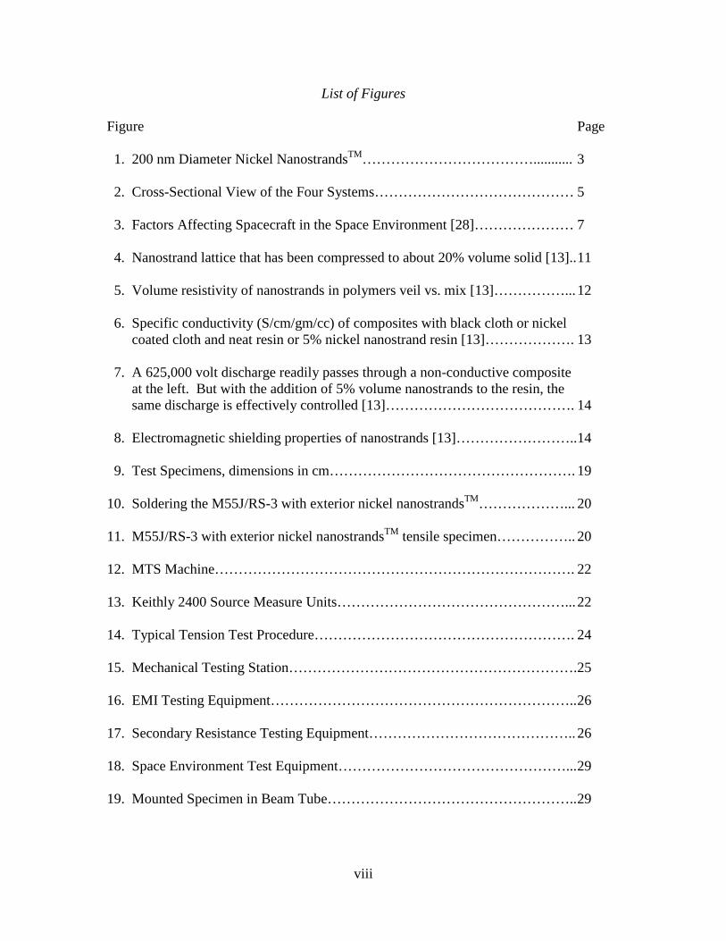
List of Figures……………………………………………………………………… viii
List of Tables………………………………………………………………………. xii
List of Symbols and Acronyms……………………………………………………..xiii
I. Introduction………………………………………………………………… 1
II. Background………………………………………………………………… 7
2.1 Overview and Challenges of the Space Environment…………………..7
2.2 Nanocomposites………………………………………………………... 9
2.3 Radiation Environments and their Damage to Materials………………. 15
2.4 Summary……………………………………………………………….. 17
III. Method of Experimentation………………………………………………... 18
3.1 Introduction…………………………………………………………….. 18
3.2 Specimen Preparation………………………………………………….. 18
3.3 Monotonic Tension and Resistance Test Equipment and Procedures…. 21
3.4 EMI Test Equipment and Procedures………………………………….. 25
3.5 Simulated Space Environment Test Equipment and Procedures………. 28
3.6 Test Plan………………………………………………………………...29
IV. Analysis and Results……………………………………………………….. 31
4.1 Introduction…………………………………………………………….. 31

vii
Page
4.2 Monotonic Tension and Resistance……………………………………. 32
4.3 EMI Shielding………………………………………………………….. 37
4.4 Simulated Space Environment…………………………………………. 41
4.5 Failure Mechanisms……………………………………………………. 45
V. Conclusions and Recommendations……………………………………….. 59
5.1 Summary……………………………………………………………….. 59
5.2 Conclusions…………………………………………………………….. 60
5.3 Recommendations for Future Work…………………………………….62
Appendix A. Stress-Strain Curves of 15.25 cm (6 in) Specimens……………….. 63
Appendix B. Stress-Strain Curves of 7.62 cm (3 in) Specimens………………… 69
Appendix C. Additional SEM Micrographs and Photos…………………………. 71
Bibliography……………………………………………………………………….. 80
Vita…………………………………………………………………………………. 83
viii
List of Figures
Figure Page
1. 200 nm Diameter Nickel NanostrandsTM………………………………........... 3
2. Cross-Sectional View of the Four Systems…………………………………… 5
3. Factors Affecting Spacecraft in the Space Environment [28]………………… 7
4. Nanostrand lattice that has been compressed to about 20% volume solid [13].. 11
5. Volume resistivity of nanostrands in polymers veil vs. mix [13]……………... 12
6. Specific conductivity (S/cm/gm/cc) of composites with black cloth or nickel coated cloth and neat resin or 5% nickel nanostrand resin [13]………………. 13 7. A 625,000 volt discharge readily passes through a non-conductive composite at the left. But with the addition of 5% volume nanostrands to the resin, the same discharge is effectively controlled [13]…………………………………. 14 8. Electromagnetic shielding properties of nanostrands [13]…………………….. 14
9. Test Specimens, dimensions in cm……………………………………………. 19
10. Soldering the M55J/RS-3 with exterior nickel nanostrandsTM………………... 20
11. M55J/RS-3 with exterior nickel nanostrandsTM tensile specimen…………….. 20
12. MTS Machine…………………………………………………………………. 22
13. Keithly 2400 Source Measure Units…………………………………………... 22
14. Typical Tension Test Procedure………………………………………………. 24
15. Mechanical Testing Station……………………………………………………. 25
16. EMI Testing Equipment……………………………………………………….. 26
17. Secondary Resistance Testing Equipment…………………………………….. 26
18. Space Environment Test Equipment…………………………………………... 29
19. Mounted Specimen in Beam Tube…………………………………………….. 29
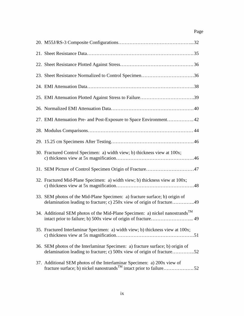
ix
Page
20. M55J/RS-3 Composite Configurations………………………………………... 32
21. Sheet Resistance Data…………………………………………………………. 35
22. Sheet Resistance Plotted Against Stress………………………………………. 36
23. Sheet Resistance Normalized to Control Specimen……………………………36
24. EMI Attenuation Data…………………………………………………………. 38
25. EMI Attenuation Plotted Against Stress to Failure…………………………….39
26. Normalized EMI Attenuation Data……………………………………………. 40
27. EMI Attenuation Pre- and Post-Exposure to Space Environment…………….. 42
28. Modulus Comparisons………………………………………………………… 44
29. 15.25 cm Specimens After Testing……………………………………………. 46
30. Fractured Control Specimen: a) width view; b) thickness view at 100x; c) thickness view at 5x magnification…………………………………………. 46 31. SEM Picture of Control Specimen Origin of Fracture…………………………47
32. Fractured Mid-Plane Specimen: a) width view; b) thickness view at 100x; c) thickness view at 5x magnification…………………………………………. 48 33. SEM photos of the Mid-Plane Specimen: a) fracture surface; b) origin of delamination leading to fracture; c) 250x view of origin of fracture………….. 49 34. Additional SEM photos of the Mid-Plane Specimen: a) nickel nanostrandsTM intact prior to failure; b) 500x view of origin of fracture……………………... 49 35. Fractured Interlaminar Specimen: a) width view; b) thickness view at 100x; c) thickness view at 5x magnification…………………………………………. 51 36. SEM photos of the Interlaminar Specimen: a) fracture surface; b) origin of delamination leading to fracture; c) 500x view of origin of fracture………….. 52 37. Additional SEM photos of the Interlaminar Specimen: a) 200x view of fracture surface; b) nickel nanostrandsTM intact prior to failure………………. 52
x
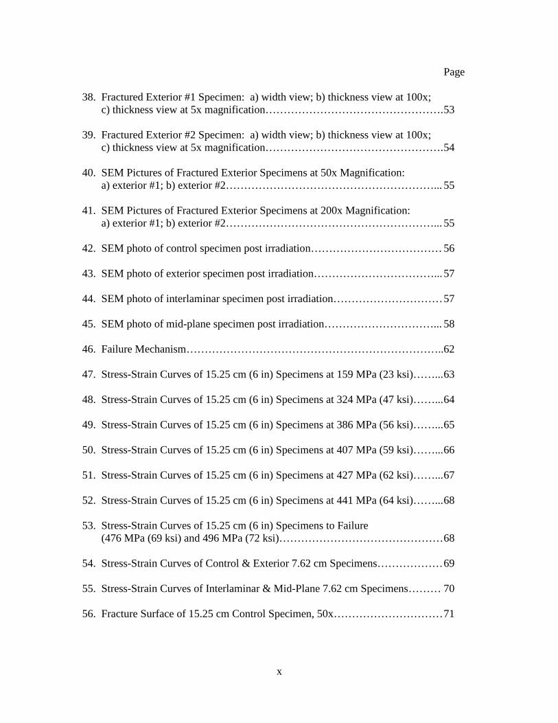
Page
38. Fractured Exterior #1 Specimen: a) width view; b) thickness view at 100x; c) thickness view at 5x magnification…………………………………………. 53 39. Fractured Exterior #2 Specimen: a) width view; b) thickness view at 100x; c) thickness view at 5x magnification…………………………………………. 54 40. SEM Pictures of Fractured Exterior Specimens at 50x Magnification: a) exterior #1; b) exterior #2…………………………………………………... 55 41. SEM Pictures of Fractured Exterior Specimens at 200x Magnification: a) exterior #1; b) exterior #2…………………………………………………... 55 42. SEM photo of control specimen post irradiation……………………………… 56
43. SEM photo of exterior specimen post irradiation……………………………... 57
44. SEM photo of interlaminar specimen post irradiation………………………… 57
45. SEM photo of mid-plane specimen post irradiation…………………………... 58
46. Failure Mechanism……………………………………………………………..62
47. Stress-Strain Curves of 15.25 cm (6 in) Specimens at 159 MPa (23 ksi)……... 63
48. Stress-Strain Curves of 15.25 cm (6 in) Specimens at 324 MPa (47 ksi)……... 64
49. Stress-Strain Curves of 15.25 cm (6 in) Specimens at 386 MPa (56 ksi)……... 65
50. Stress-Strain Curves of 15.25 cm (6 in) Specimens at 407 MPa (59 ksi)……... 66
51. Stress-Strain Curves of 15.25 cm (6 in) Specimens at 427 MPa (62 ksi)……... 67
52. Stress-Strain Curves of 15.25 cm (6 in) Specimens at 441 MPa (64 ksi)……... 68
53. Stress-Strain Curves of 15.25 cm (6 in) Specimens to Failure (476 MPa (69 ksi) and 496 MPa (72 ksi)……………………………………… 68 54. Stress-Strain Curves of Control & Exterior 7.62 cm Specimens……………… 69
55. Stress-Strain Curves of Interlaminar & Mid-Plane 7.62 cm Specimens……… 70
56. Fracture Surface of 15.25 cm Control Specimen, 50x………………………… 71
xi
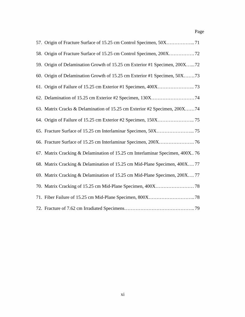
Page
57. Origin of Fracture Surface of 15.25 cm Control Specimen, 50X……………... 71
58. Origin of Fracture Surface of 15.25 cm Control Specimen, 200X……………. 72
59. Origin of Delamination Growth of 15.25 cm Exterior #1 Specimen, 200X…... 72 60. Origin of Delamination Growth of 15.25 cm Exterior #1 Specimen, 50X……. 73
61. Origin of Failure of 15.25 cm Exterior #1 Specimen, 400X………………….. 73
62. Delamination of 15.25 cm Exterior #2 Specimen, 130X……………………… 74
63. Matrix Cracks & Delamination of 15.25 cm Exterior #2 Specimen, 200X…… 74
64. Origin of Failure of 15.25 cm Exterior #2 Specimen, 150X………………….. 75
65. Fracture Surface of 15.25 cm Interlaminar Specimen, 50X…………………... 75
66. Fracture Surface of 15.25 cm Interlaminar Specimen, 200X…………………. 76
67. Matrix Cracking & Delamination of 15.25 cm Interlaminar Specimen, 400X.. 76
68. Matrix Cracking & Delamination of 15.25 cm Mid-Plane Specimen, 400X…. 77
69. Matrix Cracking & Delamination of 15.25 cm Mid-Plane Specimen, 200X…. 77
70. Matrix Cracking of 15.25 cm Mid-Plane Specimen, 400X…………………… 78
71. Fiber Failure of 15.25 cm Mid-Plane Specimen, 800X……………………….. 78
72. Fracture of 7.62 cm Irradiated Specimens…………………………………….. 79

xii
List of Tables
Table Page
1. Calibration Procedure…………………………………………………………... 27
2. Test Matrix……………………………………………………………………… 30
3. Specimen Configurations……………………………………………………….. 31
4. Summary of Tensile Test and Resistance Data………………………………….34
5. Young’s Modulus (E), UTS, and Strain Comparisons…………………………. 43

xiii
List of Symbols and Acronyms
A Area of Cross Section
E Modulus of elasticity
L Length of Electrode
R Resistance
ρ Resistivity
Rs Sheet Resistance
ε Strain
σ Stress
T Thickness of Specimen
EMI Electromagnetic Interference
ESD Electrostatic Discharge
NS Nickel NanostrandsTM
UTS Ultimate Tensile Strength
1
EVALUATION OF NANOCOMPOSITES AS LIGHTWEIGHT ELECTRONIC
ENCLOSURES FOR SATELLITES’ APPLICATIONS
I. Introduction Space offers a global prospective. The higher you are, the more of Earth’s surface
you can see. For thousands of years, kings and rulers took advantage of this fact by
putting lookout posts atop the tallest mountains to survey more of their realm and warn of
would-be attackers. Throughout history, many battles have been fought to “take the high
ground.” Space takes this quest for greater perspective to its ultimate end. From the
vantage point of space, we can view large areas of Earth’s surface. Orbiting spacecraft
can thus serve as “eyes and ears in the sky” to provide the ultimate high ground [28].
The United States military’s push for global reach and response requires that advanced
systems be deployed in orbit around the world, taking advantage of this ultimate high
ground, to aid in intelligence gathering, navigation, communications, control, remote
sensing, and other military missions. These orbiting systems have to be lighter (to
decrease launch costs), more reliable, less expensive, and operate at a higher total power
than ever before. Additionally, they need to be survivable from electromagnetic
phenomena resulting from the harsh space environment.
A spacecraft system’s structure must be strong and stiff to provide integrity
during launch as well as operations in space. Furthermore, the structure should be
capable of removing heat from the high power components and satisfy crucial
electromagnetic interference (EMI) requirements. Aluminum was the structural material

2
of choice up to the early 1990s because it is lightweight, cheap, strong, easy to machine,
and available. The aluminum structure accounted for approximately 18% of the
spacecraft’s total dry weight. Lightweight composites such as graphite/epoxy and
Kevlar/epoxy were introduced in the early 1990s to reduce the structural mass while
increasing strength and stiffness. Since costs range from $2,000 to $10,000 per pound to
launch an object into space, reducing the structural mass of the spacecraft can potentially
save hundreds of thousands of dollars in launch costs [28]. Current high performance
composite technology has reduced the structural weight to approximately 6 – 8% of the
spacecraft’s total dry weight [6]
Although these high performance structural components have dramatically
reduced weight, unfortunately they are not capable of protecting critical spacecraft
components from the harsh space environment on their own. The threats of spacecraft
charging and uncontrolled electrostatic discharge, electromagnetic interference, and
radiation from the sun can cause irreparable damages and are still critical concerns for
these spacecraft composite structures [31]. To combat these threats, current composite
spacecraft structures are electrically shielded by secondary materials such as foils,
wires/straps, and conductive paint or tape coatings. While these secondary shielding
materials are effective, they add additional manufacturing processes, are labor intensive,
and increase structural weight, resulting in an increase in cost [4, 24-25]. In order to
further reduce the spacecraft structural weight, while simultaneously eliminating the need
for secondary shielding materials, new innovative materials are needed. Recent advances
in nanocomposites offer the technology to meet this challenge.

3
Recently, the Materials and Manufacturing Directorate, Air Force Research
Laboratory, WPAFB (AFRL/RX), working with Metal Matrix Composites of Heber,
Utah have developed a new form of nano-structured nickel [1, 13]. This new material is
called nickel nanostrandsTM, which are strands of 50 ~ 1000 nm diameter nickel particles
linked in chains, microns to millimeters in length as shown in Figure 1. They are very
similar to carbon nanofibers but provide the additional features of nickel, such as
electromagnetic, chemical, catalytical and metallurgical properties. Nickel
nanostrandsTM provide a wide band of EMI shielding protection from the harsh space
Figure 1. 200 nm Diameter Nickel NanostrandsTM
environment due to their unique combination of electrical dc conductivity and
ferromagnetism. Their complex nanostructured geometry provides for a high surface
area and multiple angles of reflection and absorption. Preliminary tests conducted by
AFRL/RX have shown that a thin film (0.1016 mm) containing 20% volume fraction of
nickel nanostrandsTM in polyimide is capable to shield about 80 decibels between the
frequencies of 8 to 12 GHz with dc conductivity of 1,400 S/cm. Furthermore, this thin
film has also survived a simulated space environment and was tested to shield 75 decibels

4
with a dc conductivity of 1,100 S/cm after this exposure [2]. However, many more
studies are needed to fully understand the nanocomposites behavior for spacecraft
applications because spacecraft deployed for military purposes must be engineered to
survive the harshest space environments as orbit and apogee are dictated by operational
requirements regardless of any temporal or geospatial radiation condition. This study is a
step in this direction.
This thesis focuses on the synergism and interrelationship between the EMI
shielding protection capability and mechanical properties before and after exposure to the
space environment of nickel nanostrandsTM when used in conjunction with M55J/RS-3
composite (i.e. graphite fiber in a toughened polycyanate resin matrix). Four different
systems were tested for their ultimate tensile strength and EMI shielding protection
properties before and after exposure to a representative five year space environment to
determine their effectiveness in space operations. The four systems were additionally
tested for their EMI shielding protection and resistive properties before, during and after
monotonic tension tests of increasing loads up to fracture to determine what effect the
tensile loading conditions have on EMI shielding protection and resistivity.
The systems include a baseline control panel of M55J/RS-3 and three systems
with different layers of nickel nanostrandsTM to determine which are superior for use in
space. The four systems are shown in Figure 2. The baseline control specimen consists
of a composite configuration of M55J/RS-3 in an 8-ply, quasi-isotropic, balanced
symmetric lay-up of [0/90/±45]s with a corresponding fiber volume fraction, Vf, of 0.717.
The three additional systems with nickel nanostrandsTM (NS) include: mid-plane,
exterior, and interlaminar. The mid-plane specimen has 200 grams per square meter

5
(GSM) of NS located at the mid-plane of the baseline. The exterior specimen has 100
GSM of NS each located at the top and bottom surfaces of the baseline. The interlaminar
has four layers, each 50 GSM of NS, located between every second ply as Figure 2
indicates.
Figure 2. Cross-Sectional View of the Four Systems

6
A variety of research is being done into several areas of nanocomposites, but none
that covers nickel nanostrandsTM in conjunction with M55J/RS-3 composites and their
potential ability to reduce spacecraft structural weight (i.e. launch costs) while
simultaneously providing protection from the harmful space environment alone. The
following chapters will provide background information on nanocomposites used in
spacecraft structural applications and the harmful space environment, details of the
methodology behind the specific tests conducted with this research, analysis and results
of all tests, and will end with conclusions reached through the research in this thesis.
7
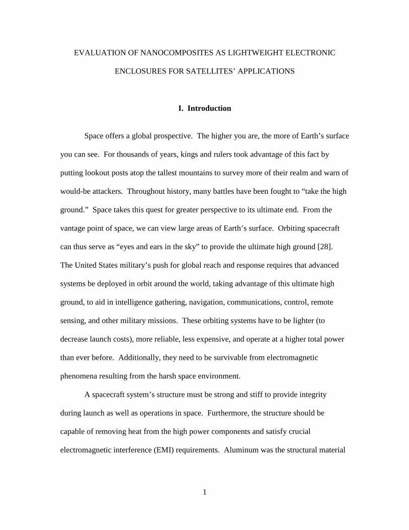
II. Background
2.1 Overview and Challenges of the Space Environment
The space environment presents one of the most, if not the most, challenging
environments for materials design. To build spacecraft that will survive the harsh space
environment, it is paramount to understand what hazards they will face. The Earth, Sun,
and cosmos combine to provide unique challenges to spacecraft designers, as shown in
Figure 3.
Figure 3. Factors Affecting Spacecraft in the Space Environment [28]
Earth exerts a gravitational pull which keeps spacecraft in orbit but presents fluid
containment problems. The Earth’s atmosphere can cause drag, which shortens orbit
lifetimes, and is also full of atomic oxygen, which can damage exposed surfaces. In the
vacuum of space, spacecraft can experience out-gassing, cold welding, and heat transfer
problems. Out-gassing occurs when the atmospheric pressure drops to near zero, causing

8
a material to evaporate or sublimate. Cold welding is a condition that can cause metal
parts to fuse together. Heat transfer problems may occur because the only way for a
spacecraft to rid itself of heat is through radiation. Another danger to spacecraft is
micrometeoroids and space junk that can collide at high speeds to damage the spacecraft.
The final two dangers to spacecraft, that are most relevant to this study, are radiation and
charged particles from the sun. Radiation can cause heating on exposed surfaces, damage
to electronic components and disruption in communication, and solar pressure, which can
change a spacecraft’s orientation. Charged particles come from the solar wind and flares,
galactic cosmic rays, and the Van Allen radiation belts. Spacecraft charging results when
charges build up on different parts of the spacecraft as it moves through concentrated
areas of charged particles. Once this charge builds up, discharge can occur with
disastrous effects: damage to surface coatings, degrading of solar panels, loss of power,
or switching off or permanently damaging electronics [28].
As previously mentioned, the high performance composites are now routinely
used in nearly all spacecraft bus structures which had reduced the total structures’ dry
weight to approximately 6 ~ 8% to date. These lightweight composite structures carry all
inertial loads and provide stiffness and dimensional stability better than their aluminum
predecessors. Additionally, they are selected for their ability to transfer or manage waste
heat produced from the high power components of the spacecraft. Unfortunately, these
composite materials pale in comparison to aluminum when it comes to protection from
the harsh space environment. They require additional steps to electrically shield and
prevent charging and consequential discharging damage to the payload electronic
components. These additional steps add undesirable weight that drives manufacturing,

9
and most importantly, launch costs upward. To reduce the structures’ weight further
from the present levels of 6 ~ 8% of the total weight, new innovative materials are
needed. Recent advances in nanocomposites offer an opportunity to meet this challenge.
2.2 Nanocomposites
Since the advent of single-wall carbon nanotubes (SWNTs) more than a decade
ago [16], there has been significant interest in the scientific and engineering communities
to utilize the extraordinary physical and mechanical properties of numerous nano or sub-
micron size structural materials. Carbon nanotubes and nanofibers have received an
incredible amount of attention over the past five years as they are candidates for use in
several applications. They also provide tremendous opportunities in the design of
multifunctional materials systems. Particularly, they promise to provide solutions to
many vexing problems encountered during the application of traditional composite
materials. They are electrically conductive and therefore are suitable for applications that
require the capability to discharge electrostatic potentials. They provide sufficient
conductivity for electrostatic painting. Further, they shield from the radio frequency
interference (RFI) or lightening strikes while keeping or enhancing the inherent high
strength/modulus to weight ratio [27, 30]. Therefore, when combined with traditional
graphite composite materials, these nanocomposites can accomplish what traditional
aluminum did in spacecraft structures but at a much lower mass: provide mechanical
support, remove excess heat, and protect from EMI. Furthermore, the lower mass
equates to a much lower launch cost. However, there have been a very limited number of
studies which have shown that SWNTs are radiation tolerant under high energy neutrons
10
(upper atmosphere), medium energy protons (LEO), and high energy protons and iron
ions (interplanetary space) [6].
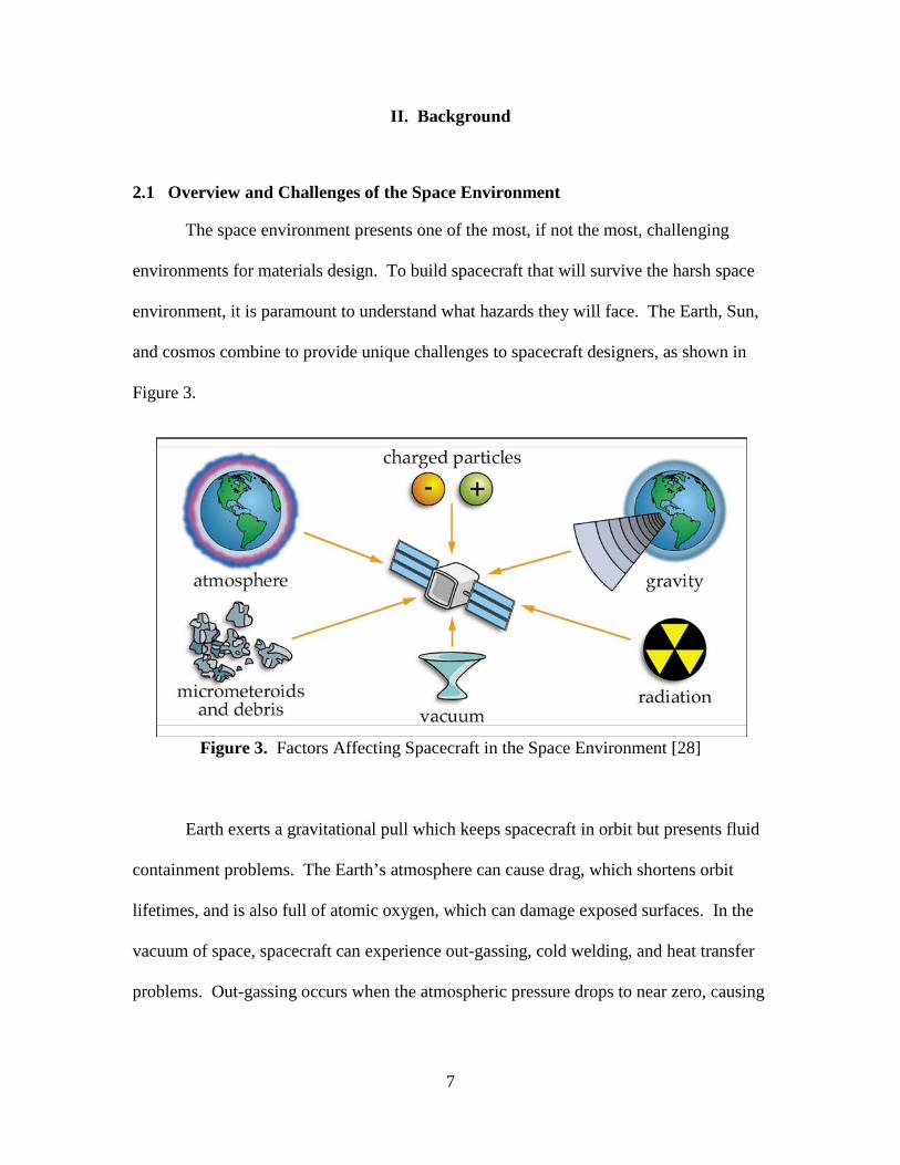
One of the major roles of carbon nanotubes and nanofibers is to make
nanocomposites a more electrically conductive material. Unfortunately, these new
materials, carbon nanofibers in particular, are sometimes limited by the intrinsic
properties of carbon and its molecular orientation in the nanostructure. Alternatively, the
highly conductive carbon nanotubes are extremely expensive to manufacture. In order to
utilize the conductive capabilities of nanotubes, the creation of a highly nanostructured
high aspect ratio filamentary pure metal is a candidate to extend the art of rendering
normally dielectric materials as conductive, especially if the nanostructure could be made
in a fully interconnected three dimensional nano-lattice. Incidentally, this lattice is
exactly what nanostrands are when they are created. As previously mentioned, the
Materials and Manufacturing Directorate, Air Force Research Laboratory, WPAFB
(AFRL/RX), working with Metal Matrix Composites of Heber, Utah as developed a new
form of nano-structured nickel. This new material, called nickel nanostrandsTM, is made
up of strands of 50 ~ 1000 nanometer diameter nickel particles linked in chains, microns
to millimeters in length. They are very similar to carbon nanofibers but provide the
additional features of nickel, such as electromagnetic, chemical, catalytical, and
metallurgical properties at less cost than SWNTs [1, 13].
When the nanostrand veil or cake is pressed by hand, it can be pressed in a
controlled fashion up to about 20% as shown in Figure 4. At this level, the conductivity
is truly extraordinary, i.e. 5000 Siemens/cm, which equates to a resistivity of 0.0002
ohm-cm. Additionally, this fine structure allows for the easy capillary infiltration into a

11
wide variety of polymers, including thermosets such as epoxy and polyimide,
thermoplastics such as polyethylene, elastomers such as silicone, thermoplastic
polyurethane, and paints such as acrylic, epoxy and urethane [13]. All of these media
have been rendered conductive. Figure 5 shows an example when nickel nanostrandsTM
are added to epoxy. The upper line in this figure is for nanostrands when mixed in a
typical way in epoxy adhesive. This exhibits volume resistivity that is similar to or better
than that of competing technologies. The lower line in this figure is typical of the volume
resistivity of the continuous nanostrand lattice that has been pressed to a
Figure 4. Nanostrand lattice that has been compressed to about 20% volume solid [13]

12
Figure 5. Volume resistivity of nanostrands in polymers veil vs. mix [13]
desired volume fraction and then infiltrated with resin, referred as a veil. The veil
exhibits volume resistivities on the order of 10-2 at very low volume fractions, and
approaches 10-4 at higher fractions. These are excellent levels of conductivity for a
composite. [13]
The advantage of adding nanostrands to a conductive fiber composite system is
that it only requires a small amount of nanostrands to create increasingly conductive
paths from fiber to fiber and throughout the resin. In addition, the nanostrands tend to fill
in a previously resin rich area of the polymer, so that even these regions are conductive.
Thus, not only can a fully conductive composite be created, the specific conductivity of
the composite can be engineered to any desired level and orientation. The dramatic
increases in composite conductivity as a function of adding nickel coated fibers or nickel
nanostrandsTM, or both, are shown in Figure 6 [13].

13
Figure 6. Specific conductivity (S/cm/gm/cc) of composites with black cloth or nickel coated cloth and neat resin or 5% nickel nanostrand resin [13]
Nickel nanostrandsTM also show promising capabilities of electrostatic dissipation
(ESD) and electromagnetic interference (EMI) shielding protection which is crucial in the
space environment. With respect to ESD, the nanostrands provide sufficient
conductivity, even in low concentrations, to stop a hefty discharge. As shown in Figure
7, a small concentration of nanostrands in an otherwise non-conductive system (silicon
rubber on a polyester cloth), provided conductive protection against a 625,000 volt
discharge [13]. Nickel nanostrandsTM are also effective in shielding electromagnetic
radiation. Preliminary studies have also shown that they provide a wide band of EMI
shielding protection. In Figure 8, only a few mils of a nanostrand composite film are
found to create a highly effective EMI shield across a wide band-width. While 60 dB is a
respectable shielding level, it is anticipated that thicker or more concentrated
nanostrands, particularly in concert with conductive fibers may provide for excellent

14
broadband shielding. The unique attribute of nanostrands appears to be their increasing
effectiveness at decreasing frequencies; a phenomenon which is opposite to most other
shielding materials [13].
Figure 7. A 625,000 volt discharge readily passes through a non-conductive composite at the left. But with the addition of 5% volume nanostrands to the resin, the same
discharge is effectively controlled [13]
Figure 8. Electromagnetic shielding properties of nanostrands [13]

15
2.3 Radiation Environments and their Damage to Materials
The space environment presents a hazardous radiation situation which can have
serious effects on spacecraft electronics as well as spacecraft structures. There are three
major sources of radiation: long term exposure within the Van Allen radiation belts,
galactic cosmic rays (GCR), and solar proton events (SPE). Exposure to any of these
types of radiation can drastically degrade the mechanical and electrical properties of
materials. Specifically, materials can fail and/or electronic systems can become
completely disabled due to spacecraft charging, deep dielectric charging, single event
upsets (SEUs), and high energy solar radiation particles. This is most important because
the nanocomposites studied in this thesis will be the first line of defense for the spacecraft
structure in the harsh space environment.
Technically, spacecraft charging is a variation in the electrostatic potential of a
spacecraft surface with respect to the surrounding plasma caused by photoemission and
plasma bombardment. Although the buildup of large static charges may confuse or blind
certain sensors, the real danger lies in the resulting discharge because structural damage
is a real possibility. Even weak discharges have been related to a variety of problems
which include: spurious electronic switching activity (such as turning off a recorder or
activating a radio), breakdown of vehicle thermal coatings, amplifier and solar cell
degradation, and degradation of optical sensors [31].
Deep dielectric charging occurs when electrons with energies between 2 and 10
MeV have enough energy to burrow deep into satellite surfaces. This excess charge
spreads out evenly on conducting surfaces, but the charge accumulates on dielectric
surfaces resulting in uneven electric potential between different portions of the satellite.

16
Eventually, potential differences can reach the breakdown threshold and a static
discharge will then occur. Unlike surface charging, deep dielectric charging can form
strong potential differences on the inside surfaces of satellites, and thus the resulting
discharges can arc directly into the satellite’s internal electrical circuitry [31].
Single event upsets (SEUs) are bit flips in digital microelectronic circuits. SEUs
can cause: damage to stored data, damage to software, the central processing unit (CPU)
to halt, the CPU to write over critical data tables, and various unplanned events due to
faulty commands. SEUs in spaceborne electronics are caused by the direct ionization of
silicon material by a high energy ion passing through it. The near Earth particle
environment includes GCR, energetic particles from the Sun, and trapped protons. The
normal factor in SEU production is the heavy ion cosmic ray, although large solar flares
can produce a substantial increase in SEUs. Fortunately, such large flares occur only
once every few years [31].
At high altitudes (geostationary orbit, GEO), solar radiation accounts for the
majority of radiation exposure. The two primary phenomena that present the solar
radiation environment are solar flare events (SFEs) and corona mass ejections (CMEs).
These events are highly unpredictable but activity commonly comes and goes based on
the 22 year solar cycle. What is predictable from two events is the type of radiation they
present to spacecraft. Generally, SFEs and CMEs exhibit a large flux of high-energy
solar protons, electrons, and alpha particles enhancing an already steady flow from
typical solar activity. These particles are the primary source of damage in the natural
space environment [31].

17
2.4 Summary
The natural space environment poses many threats to spacecraft structures as well
as electronics. The most dangerous threats are radiation and spacecraft charging which
can lead to catastrophic failure of spacecraft structure and/or electronics. It is paramount
that any improvements made in spacecraft structures provide EMI shielding protection
and be highly conductive to avoid ESD. Nickel nanostrandsTM coupled with a M55J/RS-
3 composite have the potential to eliminate these risks.

18
III. Method of Experimentation
3.1 Introduction
The purpose of this chapter is to explain precisely how the tests were run so they
may be easily repeated in future research efforts. Topics covered in this chapter include:
cutting and preparing the specimens, tensile test and resistance measurement equipment
and procedures, electromagnetic interference (EMI) test equipment and procedures,
simulated space environment test equipment and procedures, and the test plan for this
study.
3.2 Specimen Preparation
The M55J/RS-3 nickel nanostrandTM specimens used for this research effort were
cut from a 15.25 x 15.25 cm (6 x 6 in) panel by the AFIT machine shop using a high
pressure waterjet cutter. To prevent edge delamination, the panel was sandwiched
between two thin plastic sheets with double sided adhesive tape. Average thickness of
the panel was 1.016 mm (0.04 in). Rectangular shaped specimens of constant
rectangular cross-section were used in all tests. The nominal size of specimens was 15.25
x 2.7 x 0.1016 cm. Monotonic tensile and EMI tests were conducted with 15.25 cm
coupons with copper tape laminated at both ends of the composite in order to measure the
resistance across samples. However, space environment tests utilized 7.62 cm (3 in)
coupons cut out of a 15.25 cm coupon with the copper tape removed in order to fit into
the test apparatus and to maximize the number of samples. These specimen geometries
are shown in Figure 9.
19
Figure 9. Test Specimens, dimensions in cm.
After machining, the specimens were cleaned to remove any debris created during
the cutting process, ensuring a good clean bond between the glass/epoxy tabs and the
specimens at the gripping sections. These glass/epoxy tabs are necessary to protect the
specimen against possible surface cracks caused by the grips of the tensile testing
machine that could lead to premature failure. The 2.54 x 2.7 cm (1 x 1.0625 in) tabs were
attached to the specimens using M-Bond 200 adhesive.
The last step in preparing the specimens for testing was to solder solid core
copper wire to the copper tabs in order to be able to measure the resistance before,
during, and after each monotonic tension test. The soldering technique is shown in
Figure 10. Once soldering was complete, electrical tape was wrapped around the
soldered area numerous times to provide protection and stability. A final soldered and
tabbed specimen can be seen in Figure 11.

20
Figure 10. Soldering the M55J/RS-3 with exterior nickel nanostrandsTM
Figure 11. M55J/RS-3 with exterior nickel nanostrandsTM tensile specimen.
21
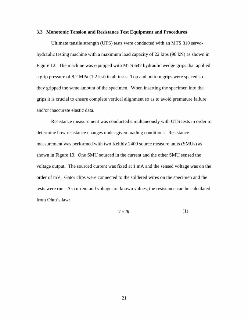
3.3 Monotonic Tension and Resistance Test Equipment and Procedures
Ultimate tensile strength (UTS) tests were conducted with an MTS 810 servo-
hydraulic testing machine with a maximum load capacity of 22 kips (98 kN) as shown in
Figure 12. The machine was equipped with MTS 647 hydraulic wedge grips that applied
a grip pressure of 8.2 MPa (1.2 ksi) in all tests. Top and bottom grips were spaced so
they gripped the same amount of the specimen. When inserting the specimen into the
grips it is crucial to ensure complete vertical alignment so as to avoid premature failure
and/or inaccurate elastic data.
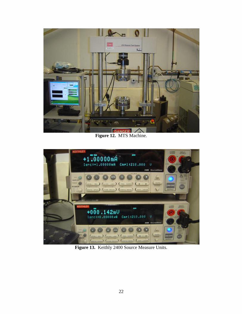
Resistance measurement was conducted simultaneously with UTS tests in order to
determine how resistance changes under given loading conditions. Resistance
measurement was performed with two Keithly 2400 source measure units (SMUs) as
shown in Figure 13. One SMU sourced in the current and the other SMU sensed the
voltage output. The sourced current was fixed at 1 mA and the sensed voltage was on the
order of mV. Gator clips were connected to the soldered wires on the specimen and the
tests were run. As current and voltage are known values, the resistance can be calculated
from Ohm’s law:
IRV = (1)
22
Figure 12. MTS Machine.
Figure 13. Keithly 2400 Source Measure Units.

23
Tensile tests for this study were run in a laboratory at room temperature. Prior to
mechanical testing, the MTS 810 machine was warmed up by cycling the actuator in the
displacement control mode for 20-30 minutes to ensure the hydraulic fluid was at
operating temperature. Per the manufacturer’s recommendation, the function generator
was programmed to deliver a cyclic command in displacement control using a square
wave at a frequency of 3 Hz and amplitude of 0.0762 mm (0.003 in). Once the MTS
810 machine was warmed up, the grips were brought to the appropriate testing height,
and the specimen was mounted and checked for proper positioning and alignment. Once
both top and bottom grips were closed the force was zeroed using the force control mode
and the MTS clip-on strain gage was mounted to the specimen and strain was also zeroed
before running the test.
Before beginning the tension test, the Keithly 2400 SMUs were connected to the
four soldered wires on the specimen with gator clips in order to source the 1 mA current
and sense the mV voltage. The SMUs were connected to a separate laptop computer,
courtesy of the Materials and Manufacturing Directorate of the Air Force Research
Laboratory (AFRL/RX), which had a program set to record the voltage, current, and
resistance data once every half second in mV, mA, and mΩ respectively during the
tension test. The MTS Multipurpose Testware (MPT) software allowed for the
programming of automated test procedures and facilitated real time data collection.
Procedures were written in a manner so that after the specimen was in place, the test ran
autonomously to the end of the procedure or until specimen failure. An example of a
typical tension test procedure is shown in Figure 14.
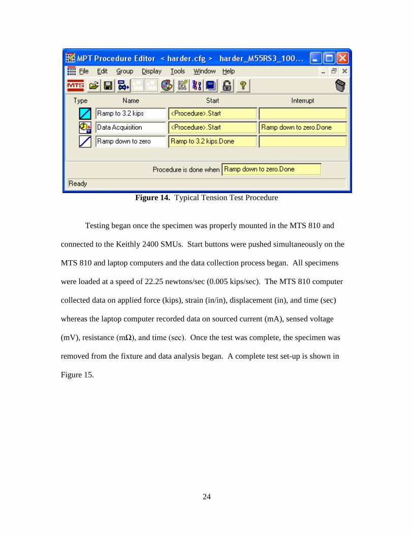
24
Figure 14. Typical Tension Test Procedure
Testing began once the specimen was properly mounted in the MTS 810 and
connected to the Keithly 2400 SMUs. Start buttons were pushed simultaneously on the
MTS 810 and laptop computers and the data collection process began. All specimens
were loaded at a speed of 22.25 newtons/sec (0.005 kips/sec). The MTS 810 computer
collected data on applied force (kips), strain (in/in), displacement (in), and time (sec)
whereas the laptop computer recorded data on sourced current (mA), sensed voltage
(mV), resistance (mΩ), and time (sec). Once the test was complete, the specimen was
removed from the fixture and data analysis began. A complete test set-up is shown in
Figure 15.
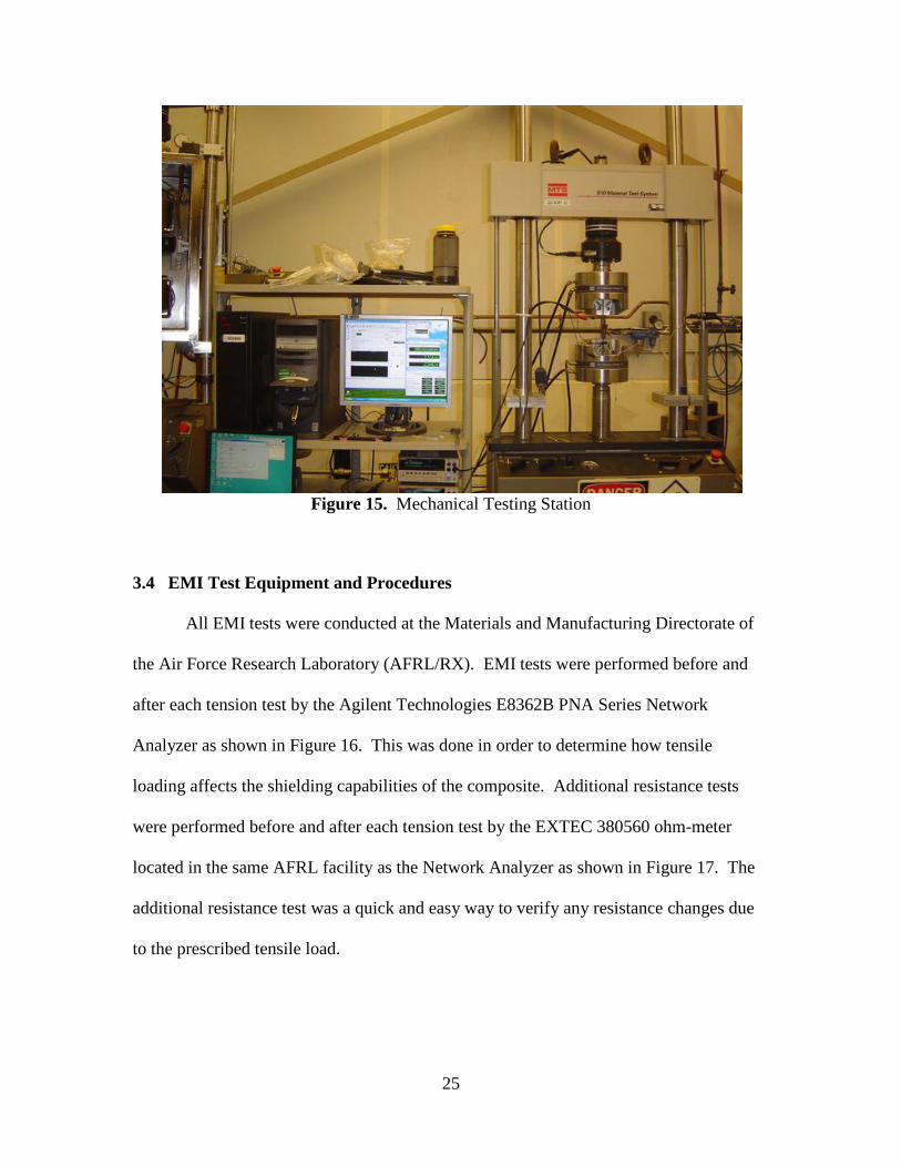
25
Figure 15. Mechanical Testing Station
3.4 EMI Test Equipment and Procedures
All EMI tests were conducted at the Materials and Manufacturing Directorate of
the Air Force Research Laboratory (AFRL/RX). EMI tests were performed before and
after each tension test by the Agilent Technologies E8362B PNA Series Network
Analyzer as shown in Figure 16. This was done in order to determine how tensile
loading affects the shielding capabilities of the composite. Additional resistance tests
were performed before and after each tension test by the EXTEC 380560 ohm-meter
located in the same AFRL facility as the Network Analyzer as shown in Figure 17. The
additional resistance test was a quick and easy way to verify any resistance changes due
to the prescribed tensile load.

26
Figure 16. EMI Testing Equipment
Figure 17. Secondary Resistance Testing Equipment

27
The Network Analyzer for EMI measurement must be properly calibrated before
each set of testing. The purpose of the calibration is to determine several undesired
parameters that may be removed or suppressed from the test sample data by subsequent
mathematical operations. When properly calibrated (measured) for each frequency in the
data set, these undesired parameters include the effects of the directivity of and reflection
from the couplers, reflections due to mismatches in the input and output test lines, and
direct coupling of signals between the input and output ports of the device along external
bypass routes [17]. A complete step-by-step calibration procedure is presented in Table
1.
Table 1. Calibration Procedure
After calibration was complete EMI testing began. It was critical to measure the
EMI attenuation in exactly the same spot on the sample test after test in order for the data
to be accurate. Therefore a red wax marker was used to draw a line on each specimen,
that when inserted in the sample holder, accurately lined up with the top. This ensured
1 Open Network Analyzer software2 File, recall previous test3 Set frequency range to: yellow = 8.2 GHz; green = 12.4 GHz4 Select Calibration Wizzard5 Click the boxes for: unguided, TRL, 1-2 ports, and cal kit #286 Click Next, Through Standard, & Line Standard7 Clamp the SHORT piece into the sample holder (piece without middle holes)8 Click both SHORT buttons9 Remove SHORT piece
10 Clamp LINE piece into the sample holder (thickest piece with middle holes)11 Click LINE button; select X-Band 1/4 wavelength line; select Next12 Remove LINE piece13 Clamp the ends of the sample holder together with nothing in between14 Click THRU15 Click Next16 Click Finish

28
repeated testing was performed on the same area of the specimen. After the specimen
was clamped to the sample holder and properly aligned with the red line, each of the four
windows on the computer screen was right-clicked and auto-scale was selected. This
provided the EMI attenuation data measurement in decibels (dB) where the larger the
number the better. The EMI measurements were not absolute values but were recorded
after each successive tension test as deltas or changes. This was due to the scattering on
the macroscopic carbon fibers. If testing a slightly different spot on the specimen the
standing wave would be scattered differently because the fibers act like diffraction
gratings.
3.5 Simulated Space Environment Test Equipment and Procedures
Simulated space environment testing was conducted at Wright State University
(WSU) with a High Voltage Engineering, Europa, Electron Van de Graaf Accelerator,
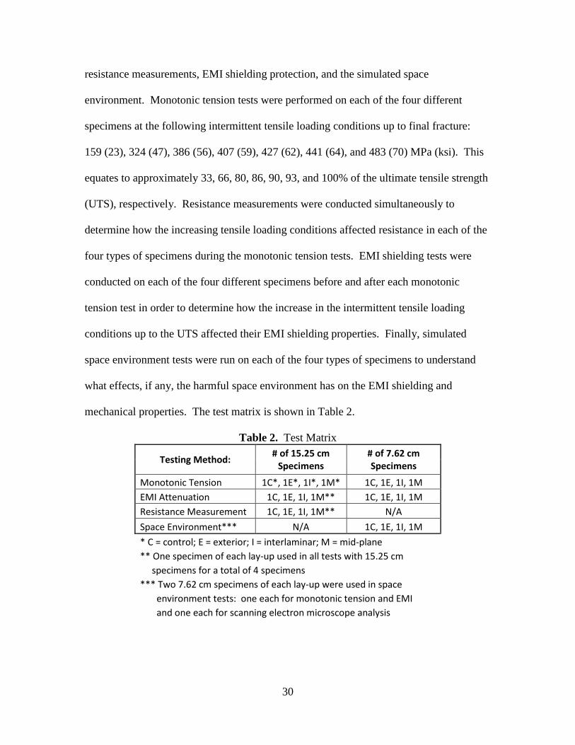
model number SN-A94 as shown in Figure 18. All irradiations were performed by the
WSU operating staff. The 7.62 cm (3 in) specimens were mounted onto a conductive
copper sample station at the end of the electron beam using a silicon paste as shown in
Figure 19. The mount was affixed to the beam tube and the chamber was evacuated to
10-7 Torre for 24 hours. The specimen was irradiated with 1.2 MeV electrons which were
scanned across the surface utilizing a steering magnet in a 3.175 cm (1.25 in) diameter
spot across the midsection of the specimen. The total electron fluence was 1014
electrons/cm2. Specimens were irradiated for approximately five minutes which
produced a simulated five year exposure to the space environment. After this exposure to
the electrons, the specimens were tested for EMI shielding properties as well as ultimate
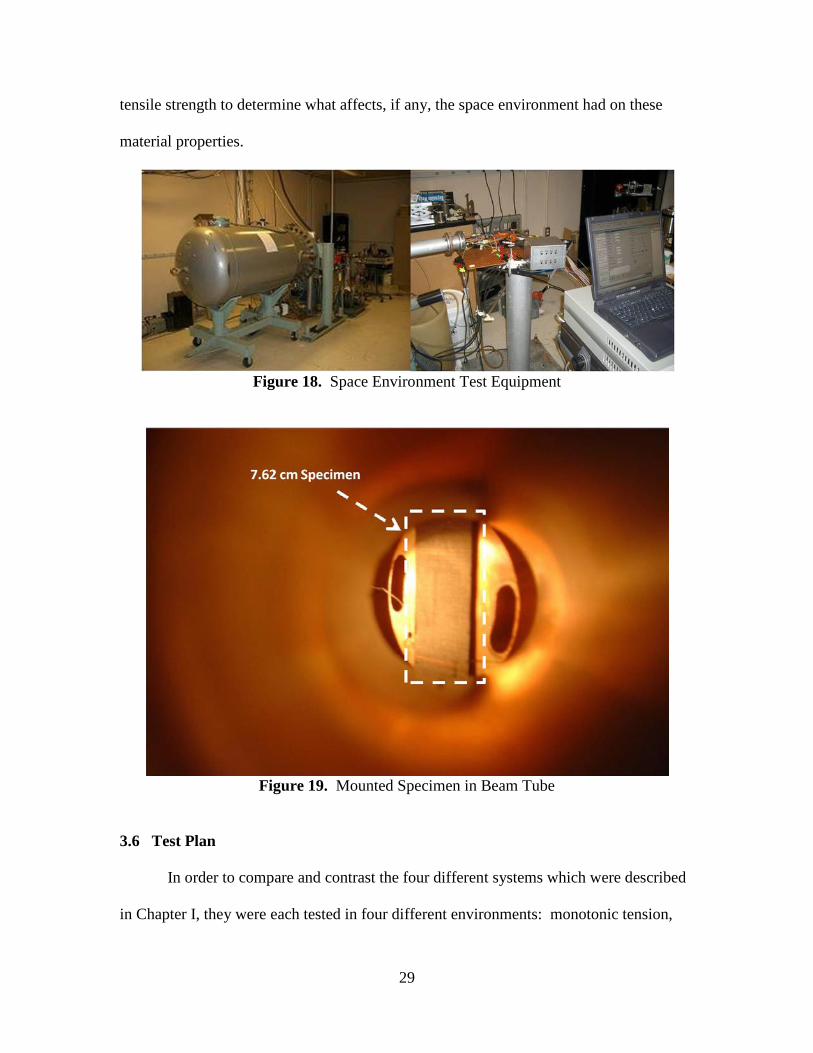
29
tensile strength to determine what affects, if any, the space environment had on these
material properties.
Figure 18. Space Environment Test Equipment
Figure 19. Mounted Specimen in Beam Tube
3.6 Test Plan
In order to compare and contrast the four different systems which were described
in Chapter I, they were each tested in four different environments: monotonic tension,
30
resistance measurements, EMI shielding protection, and the simulated space
environment. Monotonic tension tests were performed on each of the four different
specimens at the following intermittent tensile loading conditions up to final fracture:
159 (23), 324 (47), 386 (56), 407 (59), 427 (62), 441 (64), and 483 (70) MPa (ksi). This
equates to approximately 33, 66, 80, 86, 90, 93, and 100% of the ultimate tensile strength
(UTS), respectively. Resistance measurements were conducted simultaneously to
determine how the increasing tensile loading conditions affected resistance in each of the
four types of specimens during the monotonic tension tests. EMI shielding tests were
conducted on each of the four different specimens before and after each monotonic
tension test in order to determine how the increase in the intermittent tensile loading
conditions up to the UTS affected their EMI shielding properties. Finally, simulated
space environment tests were run on each of the four types of specimens to understand
what effects, if any, the harmful space environment has on the EMI shielding and
mechanical properties. The test matrix is shown in Table 2.
Table 2. Test Matrix
Testing Method: # of 15.25 cm Specimens
# of 7.62 cm Specimens
Monotonic Tension 1C*, 1E*, 1I*, 1M* 1C, 1E, 1I, 1M EMI Attenuation 1C, 1E, 1I, 1M** 1C, 1E, 1I, 1M Resistance Measurement 1C, 1E, 1I, 1M** N/A Space Environment*** N/A 1C, 1E, 1I, 1M * C = control; E = exterior; I = interlaminar; M = mid-plane ** One specimen of each lay-up used in all tests with 15.25 cm specimens for a total of 4 specimens *** Two 7.62 cm specimens of each lay-up were used in space environment tests: one each for monotonic tension and EMI and one each for scanning electron microscope analysis

31
IV. Analysis and Results
4.1 Introduction
This chapter reports the experimental results obtained during the course of this
research. In order to compare and contrast the four different systems, they were each
tested in four different environments: monotonic tension, resistance measurements, EMI
shielding protection, and the simulated space environment. Every specimen had a
baseline composite configuration of M55J/RS-3 with a 8-ply, quasi-isotropic, balanced
symmetric lay-up of [0/90/±45]s and a corresponding fiber volume fraction, Vf, of 0.717.
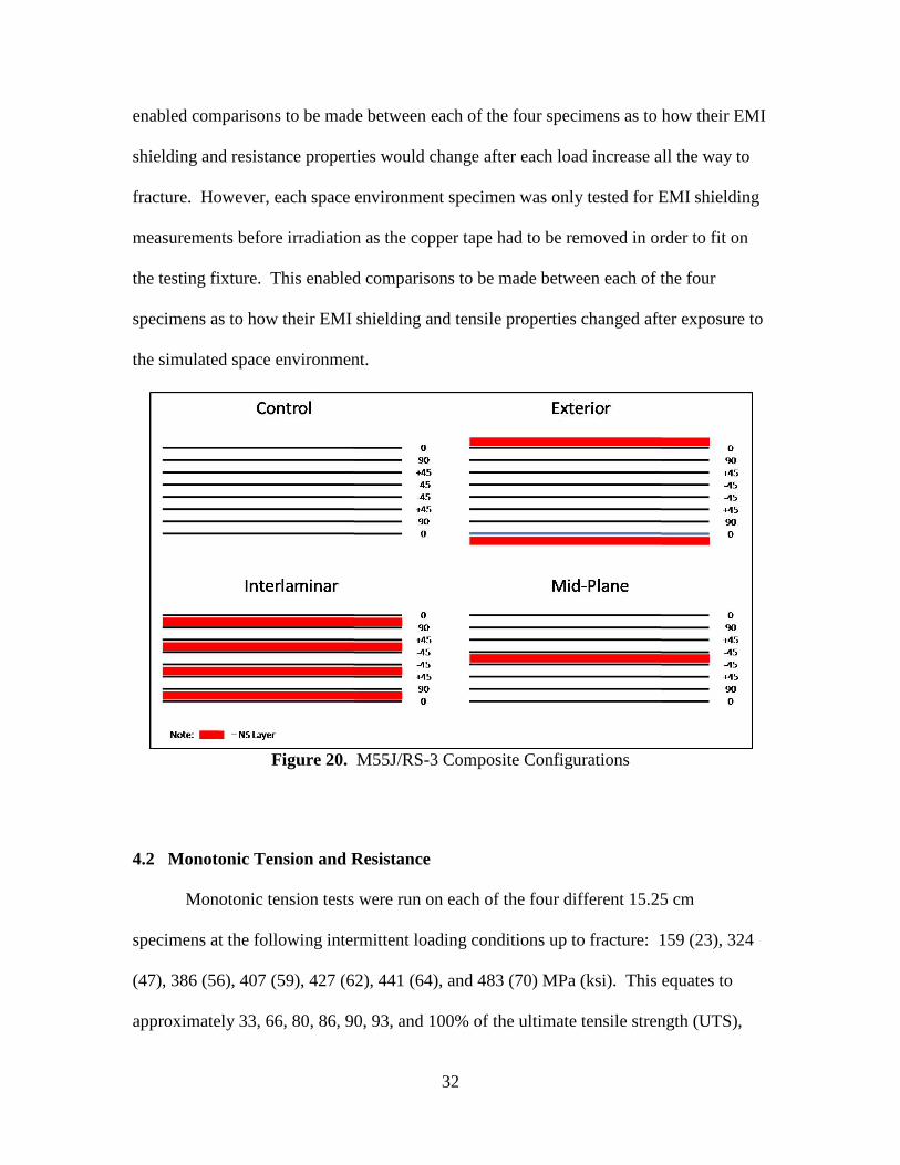
Three additional systems having nickel nanostrandsTM (NS) layers were also tested which
had these layers at: mid-plane, exterior, and distributed evenly at four interlaminar
levels. The last one will be referred to as interlaminar for the sake of brevity. The mid-
plane specimen had 200 grams per square meter (GSM) of NS located at the mid-plane of
the baseline. The exterior specimen had 100 GSM of NS each located at the top and
bottom surfaces of the baseline. The interlaminar specimen had four layers, each 50
GSM of NS, located between every second ply as shown in Table 3 and Figure 20. Each
NS lay-up had 200 GSM NS total and the lay-ups are shown in Table 3 from one surface
(ply) to the other one.
Table 3. Specimen Configurations Panel TypeControl 0 90 45 -45 -45 45 90 0Exterior (100 GSM NS) 0 90 45 -45 -45 45 90 0 (100 GSM NS)Mid-Plane 0 90 45 -45 (200 GSM NS) -45 45 90 0Interlaminar 0 (50 GSM NS) 90 45 (50 GSM NS) -45 -45 (50 GSM NS) 45 90 (50 GSM NS) 0
Composite Configurations
Each tension specimen was tested for EMI shielding and resistance measurements
before monotonic tension testing began in order to establish the baseline values. This
32
enabled comparisons to be made between each of the four specimens as to how their EMI
shielding and resistance properties would change after each load increase all the way to
fracture. However, each space environment specimen was only tested for EMI shielding
measurements before irradiation as the copper tape had to be removed in order to fit on
the testing fixture. This enabled comparisons to be made between each of the four
specimens as to how their EMI shielding and tensile properties changed after exposure to
the simulated space environment.
Figure 20. M55J/RS-3 Composite Configurations
4.2 Monotonic Tension and Resistance
Monotonic tension tests were run on each of the four different 15.25 cm
specimens at the following intermittent loading conditions up to fracture: 159 (23), 324
(47), 386 (56), 407 (59), 427 (62), 441 (64), and 483 (70) MPa (ksi). This equates to
approximately 33, 66, 80, 86, 90, 93, and 100% of the ultimate tensile strength (UTS),

33
respectively. Resistance tests were conducted simultaneously to determine how the
tensile loading conditions affected resistance in each of the four types of specimens
during the monotonic tension tests. Note that there are two exterior samples due to the
fact that exterior #1 was accidentally tested to failure on the third tension test stage.
However, the properties of both exterior samples mirror each other which show that there
was minimal scatter between replicate tests. The control specimen fractured on the fourth
loading cycle at a stress level of 407 MPa (59 ksi). The interlaminar specimen fractured
on the fifth loading cycle at a stress level of 414 MPa (60 ksi). The exterior #2 and mid-
plane specimens fractured on the seventh loading cycle at a stress level of 476 and 496
MPa (69 and 72 ksi), respectively. Stress-strain curves for all 15.25 cm specimens and
loading levels are shown in Appendix A.
The resistance values utilized in this thesis were measured from the EXTEC
380560 ohm-meter. Resistance values were measured before and after each tension test.
During the monotonic tension tests, the maximum and minimum values of resistances
were within ± 0.015 ohms from the average values and were on the average only 0.007
ohms away from the mean. This means that resistance does not fluctuate a large amount
throughout monotonic tensile loading conditions since resistance values fluctuate at only
± 6% of the mean values. Thus resistance did not fluctuate considerably throughout the
tension tests. Table 4 summarizes these testing results. Although the unit of sheet
impedance is ohms, measured results are typically labeled ohms per square to emphasize
that a thin sheet, not a lumped element, was measured [17]. Therefore, resistance values
recorded in ohms were converted to sheet resistance values in ohms per square, utilizing
the following two equations for resistivity (ρ) and sheet resistance (Rs):

34
LRA
=ρ (2)
where R = resistance; A = cross sectional area; L = electrode length, and
TRs
ρ= (3)
where T = specimen thickness.
Table 4. Summary of Tensile Test and Resistance Data

35
Sheet resistance values of all four specimen types are compared in Figures 21 to
23. Figures 21 and 22 illustrate that sheet resistance slightly increases in the interlaminar
and mid-plane specimens as stress levels increase up to the UTS, whereas sheet resistance
remains relatively constant for the control and exterior samples. This is due to the fact
that the highly conductive nanostrands on the exterior specimens carry the current
directly across the exterior nanostrand surfaces without having to go through the
thickness of the composite panel. Current must pass through the thickness of the
interlaminar and mid-plane specimens because their external surfaces are the 0° plies of
M55J/RS-3.
Figure 21. Sheet Resistance Data

36
Figure 22. Sheet Resistance Plotted Against Stress
Figure 23. Sheet Resistance Normalized to Control Specimen

37
Figure 23 shows the sheet resistance data normalized to that of the control
specimen. In order to normalize the data, all specimen values of sheet resistance for each
corresponding tensile loading level are divided by the control specimen’s value for sheet
resistance. This allows for a direct percentage comparison between the control and
nanostrand specimens. Before the application of any load, the sheet resistance of the
exterior specimens was 4% lower than that of the control specimen. However, the sheet
resistance of the interlaminar and mid-plane specimens was 27 and 11% higher;
respectively. After the application of the monotonic tensile loading conditions, the sheet
resistance of the exterior specimens decreased up to 11%, whereas, the sheet resistance of
the interlaminar and mid-plane specimens increased up to 38 and 14%, respectively,
when compared to the control specimen. This means that as the monotonic tensile load
increases, the exterior specimens were 11% more conductive than the control specimen
whereas the interlaminar and mid-plane specimens were 38 and 14% less conductive.
Given that conductivity is of utmost importance in the space environment in order to be
able to protect against charge buildup and subsequent electrostatic discharge (ESD), the
exterior specimens were superior to all in this regard.
4.3 EMI shielding
EMI shielding tests were run on each of the four different specimens before and
after each monotonic tension test in order to determine how the increase in the applied
stress levels up to the UTS affected their EMI shielding properties. EMI attenuation
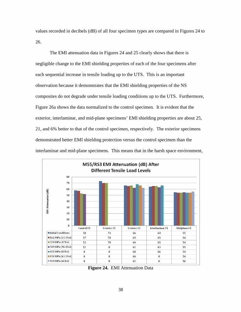
38
values recorded in decibels (dB) of all four specimen types are compared in Figures 24 to
26.
The EMI attenuation data in Figures 24 and 25 clearly shows that there is
negligible change to the EMI shielding properties of each of the four specimens after
each sequential increase in tensile loading up to the UTS. This is an important
observation because it demonstrates that the EMI shielding properties of the NS
composites do not degrade under tensile loading conditions up to the UTS. Furthermore,
Figure 26a shows the data normalized to the control specimen. It is evident that the
exterior, interlaminar, and mid-plane specimens’ EMI shielding properties are about 25,
21, and 6% better to that of the control specimen, respectively. The exterior specimens
demonstrated better EMI shielding protection versus the control specimen than the
interlaminar and mid-plane specimens. This means that in the harsh space environment,
Figure 24. EMI Attenuation Data

39
Figure 25. EMI Attenuation Plotted Against Stress to Failure
the exterior specimens outperform the other three specimens not only in terms of
conductivity as previously discussed, but in terms of EMI shielding protection as well.
Figure 26b shows the EMI data normalized to each specimen’s initial conditions. Again,
EMI shielding protection for all nanostrand specimens proved to be relatively constant
when compared to each one’s initial condition. Only the control specimen shows a
constant decrease down to 10% EMI shielding protection when compared to its original
value.

40
Figure 26. Normalized EMI Attenuation Data

41
4.4 Simulated Space Environment
Simulated space environment tests were run on each of the four types of 7.62 cm
specimens to understand what effects, if any, the harmful space environment has on the
EMI shielding and mechanical properties. EMI attenuation data was recorded pre-and
post-irradiation (1.2 MeV irradiation, which lasted five minutes) as shown in Figure 27a.
Pre-exposure measurements resulted in the exterior and mid-plane specimens
having 17 and 41% better shielding properties, respectively, when compared to the
control specimen. The interlaminar and control specimens’ values were equal. This
trend was different from the previous case because as mentioned in Chapter III, the EMI
measurements are not absolute values but are recorded as deltas or changes. Again, this
is due to the scattering on the macroscopic carbon fibers. If testing a slightly different
spot on the specimen the standing wave will be scattered differently because the fibers
are acting like diffraction gratings which will produce a different EMI attenuation value.
As expected, there was no change in the EMI shielding properties of the control
specimen post-exposure because there were no NS present to interact with the electrons.
However, all NS specimens slightly decreased their EMI shielding properties post-
exposure. The exterior, interlaminar, and mid-plane specimens EMI shielding properties
degraded 7, 6, and 2% respectively; however, the exterior and mid-plane specimens were
still 9 and 38% better, respectively, when compared to the control specimen. The
corresponding value of the interlaminar specimen was 6% less than when compared to
the control specimen. These are shown in Figure 27b where the values were again
normalized with the control specimen from pre-irradiation tests. While these values are
not absolute as previously mentioned, they do indicate that after a five year exposure to

42
the space environment, the NS specimens’ EMI shielding capabilities will slightly
degrade. Despite this slight degradation, the NS specimens will still be at an acceptable
level of EMI shielding protection.
Figure 27. EMI Attenuation Pre- and Post-Exposure to Space Environment

43
Monotonic tension tests were also conducted on post-exposure specimens to
determine what affects the simulated space environment had on the mechanical properties
of all four 7.62 cm (3 in) specimens. The irradiated control specimen was loaded until it
fractured at 496 MPa (72 ksi) with a corresponding Young’s Modulus of 110 GPa (16
MSI). The exterior, interlaminar, and mid-plane specimens each fractured in the MTS
grips at 393 (57), 221 (32), and 310 MPa (45 ksi) respectively, before reaching the
expected UTS of between 414 (60) to 496 MPa (72 ksi) as demonstrated by the 15.25 cm
(6 in) specimens. However, when compared to the 15.25 cm specimens, the irradiated
7.62 cm control specimen fractured within the expected stress range with an equivalent
Young’s Modulus. Table 5 shows Young’s Modulus, UTS, and strain comparisons
between the 15.25 and 7.62 cm specimens. Figure 28 graphically compares the Young’s
Modulus of the 7.62 cm irradiated specimens to that of the non-irradiated 15.25 cm
specimens and shows that throughout all monotonic tensile loading conditions, the
average moduli remains relatively constant. Stress-strain curves for all 7.62 cm
specimens and loading levels are shown in Appendix B.
Table 5. Young’s Modulus (E), UTS, and Strain Comparisons
Specimen Unexposed
UTS MPa (ksi)
Irradiated UTS
MPa (ksi)
Unexposed Average E GPa (MSI)
Irradiated Average E GPa (MSI)
Unexposed Strain
(mm/mm)
Irradiated Strain
(mm/mm) 15.25 cm 7.62 cm 15.25 cm 7.62 cm 15.25 cm 7.62 cm Control 408 (59) 496 (72) 112 (16.3) 110 (16) 0.0035* 0.0038 Exterior 475 (69) 393 (57)** 98 (14.2) 99 (14.4) 0.0022 0.0022* Interlaminar 414 (60) 221 (32)** 104 (15.1) 106 (15.4) 0.0042 0.0042* Mid-Plane 500 (72.5) 310 (45)** 99 (14.4) 100 (14.5) 0.0032 0.0032* * Ultimate Strain ** Fractured in the MTS grips

44
Figure 28. Modulus Comparisons
The 7.62 cm control, exterior, interlaminar, and mid-plane specimens, which
fractured prematurely in the MTS grips, demonstrated equivalent average moduli to those
of their 15.25 cm counterparts. The ultimate strain at the precise point of fracture of the
7.62 cm NS specimens also matches that of their 15.25 cm counterparts at the same levels
of stress. The 7.62 cm control specimen fractured at 496 MPa (72 ksi), which is 88 MPa
(13 ksi) larger than the 15.25 control specimen; however the ultimate strain of the 15.25
cm control specimen at a UTS of 407 MPa (59 ksi) matches strain of the 7.62 cm control
specimen. These facts, coupled with the 7.62 cm control specimen fracturing as
expected, and by utilizing the equation:
εσ Ε= (4)
in which σ = stress; E = modulus; ε = strain, allows for the extrapolation that the 7.62 cm
exterior, interlaminar, and mid-plane NS specimens fracture stresses would have been

45
within the expected stress range had they not broken in the MTS grips. This means that
the space environment does not affect the mechanical properties of all four specimens.
4.5 Failure Mechanisms
Failure Mechanisms were investigated through an optical microscope and the
SEM to determine if there are different modes of failure between the four different
systems. This section will systematically walk through each system’s mode of failure
under monotonic tensile loading. After the tension testing, all specimens showed failure
at similar places. The 15.25 cm (6 in) control, exterior, interlaminar, and mid-plane
specimens are shown in Figure 29. In order to establish a basis for comparison
throughout the remainder of the chapter, the first system under optical observation was
the control panel.
The M55J/RS-3 control specimen has a symmetric balanced lay-up consisting of
eight layers of carbon fiber M55J with a [0/90/±45]s orientation and does not have a layer
of nickel nanostrandsTM. The first step in the failure mechanism of a typical [0/90/±45]s
composite consists of transverse matrix cracking in the 90° layer. These cracks increase
in density up to a limiting value or the characteristic damage state. Thereafter, as the load
increases, cracking starts in the ± 45 plies, precipitating ultimate failure [7]. Figure 30
shows this is indeed the case. The 90° layers fractured first which lead to the ±45 plies
shear failure and then ultimate failure of the specimen.

46
Figure 29. 15.25 cm Specimens After Testing
Figure 30. Fractured Control Specimen: a) width view; b) thickness view at 100x;
c) thickness view at 5x magnification

47
In order to accurately determine the modes of failure the sample must be analyzed
from the thickness view as shown in Figures 30 b and c. From this viewpoint, the area
highlighted with arrows depicts the origin of the failure. Scanning electron microscope
(SEM) pictures were taken of the highlighted area to determine the details of the failure
mechanisms as shown in Figure 31. As mentioned earlier, the 90° fibers broke which
caused delamination in the 0/90 ply which precipitated transverse matrix cracks from the
90° ply to the ±45 ply which caused delamination directly resulting in the ±45 shear and
specimen failure.
Figure 31. SEM Picture of Control Specimen Origin of Fracture

48
The M55J/RS-3 mid-plane specimen has a symmetric balanced lay-up consisting
of eight layers of carbon fiber M55J with a [0/90/±45]s orientation combined with a layer
of nickel nanostrandsTM located at the mid-plane of the specimen as previously indicated.
Figure 32 shows the width view as well as the thickness view of the fractured specimen.
Again it is evident that the mid-plane specimen failed in the same manner as the control
specimen. SEM pictures were taken to validate the mode of failure as shown in Figures
33 and 34.
Figure 32. Fractured Mid-Plane Specimen: a) width view; b) thickness view at 100x; c) thickness view at 5x magnification

49
Figure 33. SEM photos of the Mid-Plane Specimen: a) fracture surface; b) origin of delamination leading to fracture; c) 250x view of origin of fracture
Figure 34. Additional SEM photos of the Mid-Plane Specimen: a) nickel nanostrandsTM intact prior to failure; b) 500x view of origin of fracture
The SEM pictures of the mid-plane sample indicate failure in the same manner as
the control sample with the nickel nanostrandsTM completely intact up to failure. The 90°
plies failed which resulted in delamination between the 0/90 plies which lead to

50
transverse matrix cracking causing delamination in the ±45 plies that resulted in the shear
failure of the composite. Complete ±45 shear and specimen failure is shown in Figure
33a. It is important to note that the nanostrands were undamaged up until the point of
fracture as indicated in Figure 34a. This fact leads to the conclusion that because the
nanostrands were intact until fracture, the composite would maintain its ESD and EMI
shielding capabilities until UTS, which was proved via the monotonic tension tests in
conjunction with the EMI and resistivity measurements.
The M55J/RS-3 interlaminar specimen has a symmetric balanced lay-up
consisting of eight layers of carbon fiber M55J with a [0/90/±45]s orientation combined
with 4 layers of alternating nickel nanostrandsTM evenly dispersed as previously
indicated. Figure 35 shows the width view as well as the thickness view of the fractured
surface. Again it is evident that the interlaminar specimen failed in the same manner as
the control and mid-plane specimens. SEM pictures were taken to validate the mode of
failure as shown in Figures 36 and 37.
51
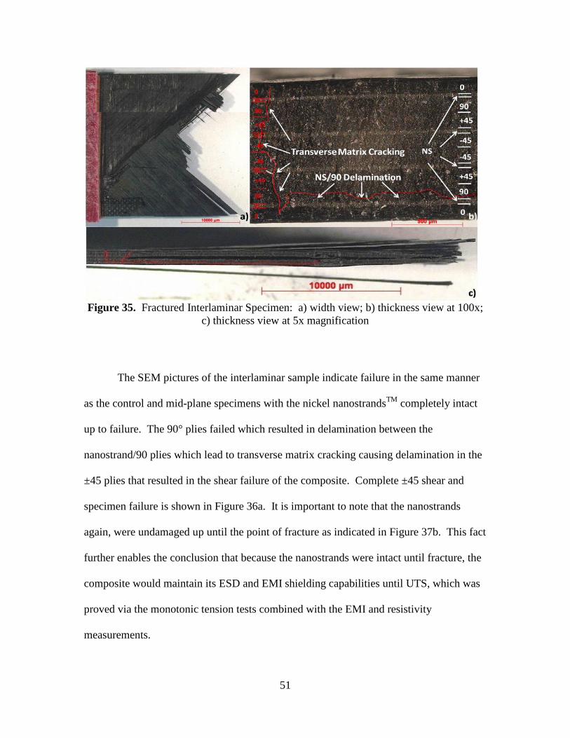
Figure 35. Fractured Interlaminar Specimen: a) width view; b) thickness view at 100x; c) thickness view at 5x magnification
The SEM pictures of the interlaminar sample indicate failure in the same manner
as the control and mid-plane specimens with the nickel nanostrandsTM completely intact
up to failure. The 90° plies failed which resulted in delamination between the
nanostrand/90 plies which lead to transverse matrix cracking causing delamination in the
±45 plies that resulted in the shear failure of the composite. Complete ±45 shear and
specimen failure is shown in Figure 36a. It is important to note that the nanostrands
again, were undamaged up until the point of fracture as indicated in Figure 37b. This fact
further enables the conclusion that because the nanostrands were intact until fracture, the
composite would maintain its ESD and EMI shielding capabilities until UTS, which was
proved via the monotonic tension tests combined with the EMI and resistivity
measurements.

52
Figure 36. SEM photos of the Interlaminar Specimen: a) fracture surface; b) origin of delamination leading to fracture; c) 500x view of origin of fracture
Figure 37. Additional SEM photos of the Interlaminar Specimen: a) 200x view of
fracture surface; b) nickel nanostrandsTM intact prior to failure

53
The two M55J/RS-3 exterior specimens had a symmetric balanced lay-up
consisting of eight layers of carbon fiber M55J with a [0/90/±45]s orientation combined
with 2 layers of nickel nanostrandsTM as the first and last plies as previously indicated.
Figures 38 and 39 show the width view and the thickness view of the fractured surfaces
from both exterior samples. Again it is evident that the exterior specimens failed in the
same manner as the control, mid-plane, and interlaminar specimens. SEM pictures were
taken to validate the mode of failure of both exterior specimens as shown in Figures 40 to
43.
Figure 38. Fractured Exterior #1 Specimen: a) width view; b) thickness view at 100x; c) thickness view at 5x magnification

54
Figure 39. Fractured Exterior #2 Specimen: a) width view; b) thickness view at 100x; c) thickness view at 5x magnification
The SEM pictures of the two exterior samples indicate failure in the same manner
as the control, mid-plane, and interlaminar specimens with the nickel nanostrandsTM
completely intact up to failure. The 90° plies failed first which resulted in delamination
between the 0/90 plies which lead to transverse matrix cracking causing delamination in
the ±45 plies that resulted in the shear failure of the composite. Complete ±45 shear and
specimen failure on both specimens is shown in Figures 40 and 41. It is important to note
that the once again, the nanostrands were undamaged up until the point of fracture. This
fact further cements the conclusion that because the nanostrands were intact until
fracture, the composite would maintain its ESD and EMI shielding capabilities until UTS,
which was proved via the monotonic tension tests coupled with the EMI and resistivity
measurements.

55
Figure 40. SEM Pictures of Fractured Exterior Specimens at 50x Magnification: a) exterior #1; b) exterior #2
Figure 41. SEM Pictures of Fractured Exterior Specimens at 200x Magnification: a) exterior #1; b) exterior #2
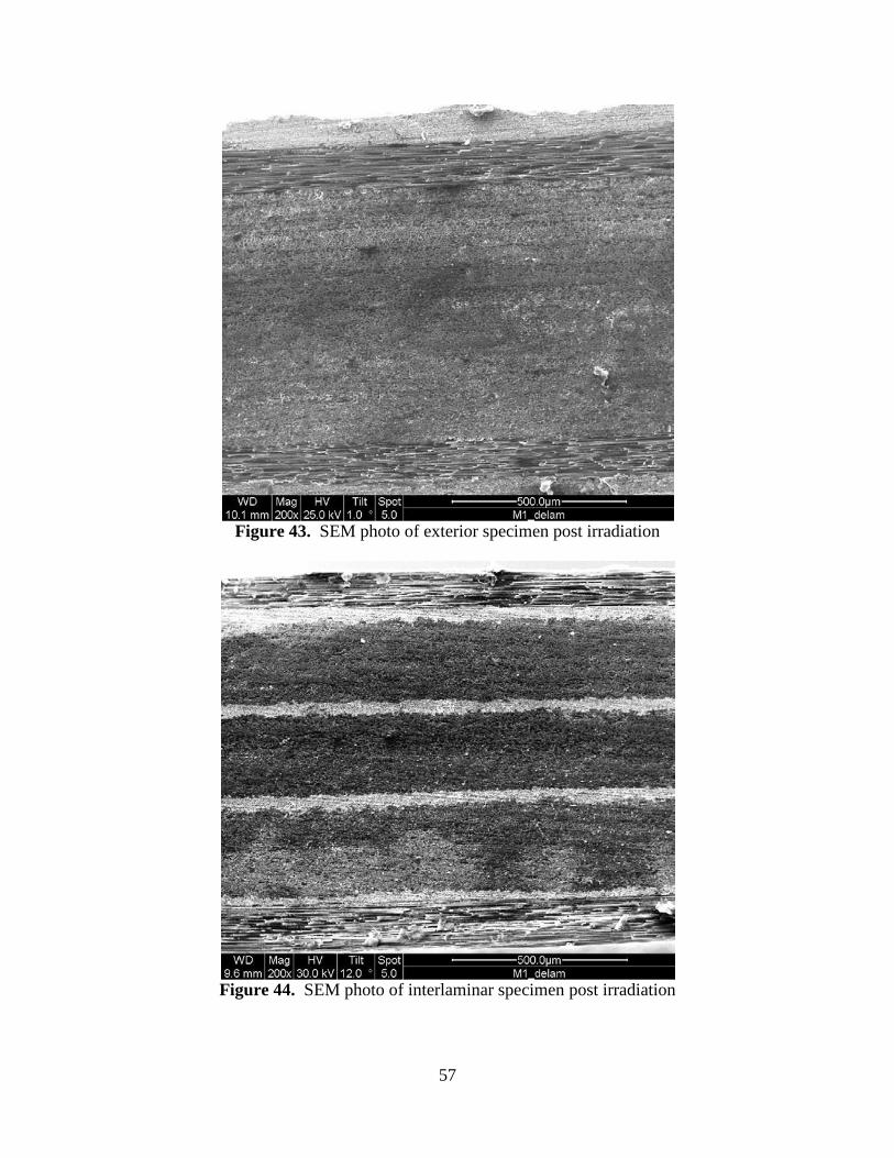
A final SEM analysis on the irradiated 7.62 cm (3 in) specimens was required in
order to determine if exposure to the space environment alone causes any unwanted
damage to the composites such as matrix cracking or more importantly, delamination
between plies. Again, each sample was irradiated with 1.2 MeV electrons which were

56
scanned across the surface utilizing a magnetic steering magnet in a 1.25 inch diameter
spot across the midsection of the specimen. The total electron fluence was 1E14
electrons/cm2; however, the interlaminar sample was accidentally irradiated with twice
the fluence at 2E14 electrons/cm2. Specimens were irradiated for approximately five
minutes which produced a simulated five year exposure to the space environment. After
the specimens were irradiated, they were each cut in half lengthwise by a diamond wet
saw in order to examine the irradiated sections for any damage. The SEM analysis of
each of the four specimens post exposure to the space environment resulted in no damage
to any of the specimens. There was no evidence of delamination or matrix cracking after
irradiation as shown in Figures 42 to 45.
Figure 42. SEM photo of control specimen post irradiation
57
Figure 43. SEM photo of exterior specimen post irradiation
Figure 44. SEM photo of interlaminar specimen post irradiation

58
Figure 45. SEM photo of mid-plane specimen post irradiation

59
V. Conclusions and Recommendations
This chapter begins with a brief summary of the experiments conducted for this
study and the analysis of their results. Next, the final conclusions of this study are
presented and explained. Finally, potential topics for future studies are suggested.
5.1 Summary
The main objective of this study was to determine if a M55J/RS-3 composite (i.e.
graphite fiber in a toughened polycyanate resin matrix) combined with nickel
nanostrandsTM would be suitable for use in satellite structure applications while
simultaneously providing ESD and EMI shielding protection from the harmful space
environment. This would further reduce the satellites’ overall dry weight and eliminate
the need for expensive additional secondary shielding materials to be applied, therefore
dramatically reducing manufacturing and launch costs. Four different composite
configurations were tested for their ultimate strength and EMI shielding protection
properties before and after exposure to a representative five year space environment. The
four configurations tested were a baseline control panel of M55J/RS-3 and three systems
with different layers of nickel nanostrandsTM added to the control specimen: exterior,
interlaminar, and mid-plane. Please remember that the four different composite
configurations are detailed in Table 3 and Figure 20. These four systems were
additionally tested for their EMI shielding protection and resistivity properties before,
during and after monotonic tension tests of increasing loads up to fracture to determine
what affect the tensile loading conditions have on EMI shielding protection and
resistivity. The test set up for these experiments was detailed in Chapter III.

60
5.2. Conclusions
From the analysis of the test results, the following conclusions can be drawn:
A. Effect of monotonic tensile loading on EMI shielding protection and sheet
resistance
• The UTS was within a range of 414 MPa (60 ksi) to 496 MPa (72 ksi) as
demonstrated by the four different composite configurations and the
nanostrands did not have any effect on the strength (UTS) or stiffness
(Young’s modulus, E) of the baseline M55J/RS-3 composite.
• EMI shielding protection capability of the four different specimens was
reasonably constant throughout the intermittent tensile loading conditions
up to failure. The exterior specimens performed better than the
interlaminar and mid-plane specimens and were 25% better at EMI
shielding protection than the control specimen.
• Sheet resistance measurements before and after the application of
increasing monotonic tensile loading conditions showed that exterior
specimens are better at ESD protection. The interlaminar and mid-plane
specimen’s sheet resistance steadily increases after each monotonic tensile
load whereas the exterior specimen’s sheet resistance is constant. This is
due to the fact that the highly conductive nanostrands on the exterior
specimens carry the current directly across the external nanostrand
surfaces without having to go through the thickness of the composite
panel. Current must pass through the thickness of the interlaminar and
mid-plane specimens because their external surfaces are the 0° plies of

61
M55J/RS-3. Since conductivity is of utmost importance in the space
environment in order to be able to protect against charge buildup and
subsequent ESD, the exterior specimens are superior to all in this regard.
B. Effect of space environment on UTS, Young’s modulus, and EMI shielding
protection
• The UTS and Young’s modulus of the specimens does not change after
exposure to the space environment. This is most likely due to the fact that
the nickel nanostrandsTM are able to provide protection from the
composite’s interaction with charged particles. This is crucial in the
harmful space environment because the spacecraft structure must be
strong (high UTS) and stiff (high E).
• The EMI shielding protection capabilities of the three nickel nanostrandTM
specimens slightly degrades (2 ~ 7%) after exposure to a five year
simulated space environment, however they still provide adequate EMI
shielding protection.
C. Failure mechanisms
• The failure mechanisms for the four specimens are the same, regardless of
composite configuration. The 90° plies failed first, which resulted in
delamination between the 0/90 plies which leads to transverse matrix
cracking causing delamination in the ±45 plies that resulted in ±45 shear
and ultimate failure of the composite as shown schematically in Figure 46.
It is important to note that the nanostrand layers remain intact up until

62
composite fracture which will be crucial in the harmful space
environment.
Figure 46. Failure Mechanism
5.3 Recommendations for Future Work
This research is the first step in the study of conductive nanocomposites for use in
satellite structure applications. Continued research into materials other than nickel
nanostrandsTM for use in conductive nanocomposites is imperative to provide the best
possible nanocomposite material combination for this application. This would lead to a
broader sample size for comparisons and would lend itself to a better grasp of the
significance of the research. The next step forward in this research effort is to perform
fatigue tests on all samples and see how that affects the ESD and EMI shielding
protection capabilities of the M55J/RS-3 nickel nanostrandTM composite configurations.

63
Appendix A: Stress-Strain Curves of 15.25 cm (6 in) Specimens
Figure 47. Stress-Strain Curves of 15.25 cm (6 in) Specimens at 159 MPa (23 ksi)

64
Figure 48. Stress-Strain Curves of 15.25 cm (6 in) Specimens at 324 MPa (47 ksi)

65
Figure 49. Stress-Strain Curves of 15.25 cm (6 in) Specimens at 386 MPa (56 ksi)

66
Figure 50. Stress-Strain Curves of 15.25 cm (6 in) Specimens at 407 MPa (59 ksi)

67
Figure 51. Stress-Strain Curves of 15.25 cm (6 in) Specimens at 427 MPa (62 ksi)

68
Figure 52. Stress-Strain Curves of 15.25 cm (6 in) Specimens at 441 MPa (64 ksi)
Figure 53. Stress-Strain Curves of 15.25 cm (6 in) Specimens to Failure
(476 MPa (69 ksi) and 496 MPa (72 ksi)

69
Appendix B: Stress-Strain Curves of 7.62 cm (3 in) Specimens
Figure 54. Stress-Strain Curves of Control & Exterior 7.62 cm Specimens

70
Figure 55. Stress-Strain Curves of Interlaminar & Mid-Plane 7.62 cm Specimens

71
Appendix C: Additional SEM Micrographs and Photos
Figure 56. Fracture Surface of 15.25 cm Control Specimen, 50x
Figure 57. Origin of Fracture Surface of 15.25 cm Control Specimen, 50X
72
Figure 58. Origin of Fracture Surface of 15.25 cm Control Specimen, 200X
Figure 59. Origin of Delamination Growth of 15.25 cm Exterior #1 Specimen, 200X

73
Figure 60. Origin of Delamination Growth of 15.25 cm Exterior #1 Specimen, 50X
Figure 61. Origin of Failure of 15.25 cm Exterior #1 Specimen, 400X

74
Figure 62. Delamination of 15.25 cm Exterior #2 Specimen, 130X
Figure 63. Matrix Cracks & Delamination of 15.25 cm Exterior #2 Specimen, 200X

75
Figure 64. Origin of Failure of 15.25 cm Exterior #2 Specimen, 150X
Figure 65. Fracture Surface of 15.25 cm Interlaminar Specimen, 50X
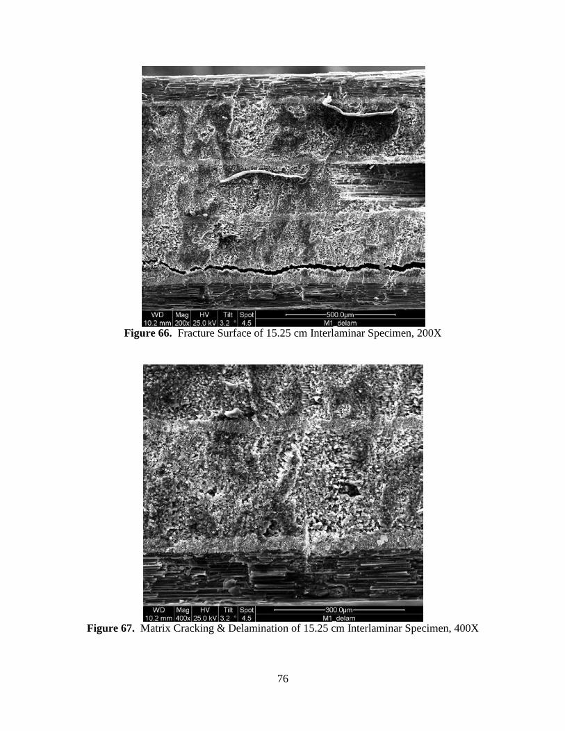
76
Figure 66. Fracture Surface of 15.25 cm Interlaminar Specimen, 200X
Figure 67. Matrix Cracking & Delamination of 15.25 cm Interlaminar Specimen, 400X

77
Figure 68. Matrix Cracking & Delamination of 15.25 cm Mid-Plane Specimen, 400X
Figure 69. Matrix Cracking & Delamination of 15.25 cm Mid-Plane Specimen, 200X

78
Figure 70. Matrix Cracking of 15.25 cm Mid-Plane Specimen, 400X
Figure 71. Fiber Failure of 15.25 cm Mid-Plane Specimen, 800X

79
Figure 72. Fracture of 7.62 cm Irradiated Specimens

80
Bibliography
[1] M. D. Alexander. Nickel NanostrandsTM Expand Nanotechnology Engineering Capabilities. Available: http://www.afrl.af.mil.
[2] M. D. Alexander, H. Dowty, B. Black, C. Cerbus, J. Henes, G. Hansen, D. Widdof and M. Pettit, "Fabrication and Space Testing of Conductive Nanocomposites Containing Carbon Nanofibers and Ni Nanostrands," in NSMMS Meeting, 2006.
[3] D. F. Bahr, H. Kung, N. R. Moody and K. J. Wahl, Mechanical Properties Derived from Nanostructuring Materials. Pennsylvania: Materials Research Society, 2003.
[4] K. L. Bedingfield, R. D. Leach and M. D. Alexander, "Spacecraft Systems Failures and Anomalies Attributed to the Natural Space Environment," NASA Reference Publication 1390, 1996.
[5] L. Capes, E. Valentin, S. Esnouf, A. Ribayrol, O. Jost, A. Filoramo and J. N. Patillon, "High Yield Non-Destructive Purification of Single Wall Carbon Nanotubes Monitored by EPR Measurements," in IEEE Conference on Nanostructures, 2002, pp. 439-442.
[6] M. Chipara, D. L. Edwards, R. S. Benson and S. Philips, "Materials for space applications," in MRS Symposium Proceedings Volume 851, 2004.
[7] I. M. Daniel and O. Ishai, Engineering Mechanics of Composite Materials. , Second ed. New York: Oxford University Press, 2006, pp. 265-266.
[8] N. E. Dowling, Mechanical Behavior of Materials. New Jersey: Prentice Hall, 2007.
[9] J. R. Gaier, United States and National Aeronautics and Space Administration, Prospects for using Carbon-Carbon Composites for EMI Shielding. Washington, DC; Springfield, Va: National Aeronautics and Space Administration; For sale by the National Technical Information Service, 1990.
[10] J. R. Gaier, United States and National Aeronautics and Space Administration, Intercalated Graphite Fiber Composites as EMI Shields in Aerospace Structures. Washington, DC; Springfield, Va: National Aeronautics and Space Administration; National Technical Information Service, distributor, 1990.

81
[11] D. Gay, S. V. Hoa and S. W. Tsai, Composite Materials Design and Applications. New York: CRC Press, 2003.
[12] K. Green, J. Petrosky, D. Weeks and W. Carlos, "Identification of Gallium-Related Electron Paramagnetic Resonance in GaN Following 1.0 MeV Electron Irradiation," Journal of Electronics, 2006.
[13] G. Hansen, "High Aspect Ratio Sub-Micron and Nano-scale Metal Filaments," SAMPE Journal, vol. 41, 2005.
[14] G. Harris, J. Lennhoff, J. Nassif, M. Vinciguerra, P. Rose, D. Jaworski and J. Gaier, "Lightweight Highly Conductive Composites for EMI Shielding," SAMPE Journal., vol. 36, pp. 59-63, 2000.
[15] H. Helvajian and E. Y. Robinson, Micro- and Nanotechnology for Space Systems. Los Angeles: The Aerospace Press, 1997.
[16] S. Ijima, "Helical Microtubules of Graphitic Carbon," Nature Physics, vol. 354, pp. 56-58, 1991.
[17] E. F. Knott, J. F. Shaeffer and M. T. Tuley, Radar Cross Section. Boston: Artech House, 1993.
[18] H. Lee, S. Mall, V. Nalladega, S. Sathish, A. Roy and K. Lafdi, "Characterization of Carbon Nanofiber Reinforced Epoxy Composite using Nanoindentation and AFM/UFM Techniques," Polymer Composites, vol. 14, pp. 549-562, 2006.
[19] N. Li, Y. Huang, F. Du, X. He, X. Lin, H. Gao, Y. Ma, F. Li, Y. Chen and P. C. Eklund, "Electromagnetic Interference (EMI) Shielding of Single-Walled Carbon Nanotube Epoxy Composites," Nano Letters, vol. 6, pp. 1141-1145, 2006.
[20] S. Mall, "Properties and Performance of Laminated Polymer Matrix Composites," in Composites Engineering Handbook P. K. Mallick, Ed. New York: Mercel Dekker, 1997, pp. 813-890.
[21] J. W. Molyneux-Child, “RFI/EMI Shielding Materials,” EMC Shielding Materials, Boston: Newnes, 1997, pp. 175.
82
[22] D. G. Moris, Mechanical Behavior of Nanostructured Materials. New Hampshire: Trans Tech Publications, 1998.
[23] H. S. Nalwa, Nanostructured Materials and Nanotechnology. New York: Academic Press, 2002.
[24] S. P. Rawal, "Multifunctional Carbon Nanocomposite Coatings for Space Structures," in AIAA SDM Conference, 2006.
[25] S. P. Rawal and F. M. Kustas, "Evaluation of Carbon Nanofiber-Based Coating and Adhesives," SAMPE Journal, 2006.
[26] S. P. 1. Rea, D. 1. Wylie, D. 1. Linton, E. Orr and J. McConnell, "EMI shielding of woven carbon fibre composites," in 2004 High Frequency Postgraduate Student Colloquium, 2004, pp. 205-10.
[27] M. J. Schulz, A. D. Kelkar and M. J. Sundaresan, Nanoengineering of Structural, Functional, and Smart Materials. New York: CRC Press, 2005.
[28] J. J. Sellers, Understanding Space. New York: McGraw-Hill, 2005, pp. 3-5, 79-89, 674-681.
[29] E. Silverman, "Space Environmental Effects on Spacecraft: LEO Materials Selection Guide," NASA, Tech. Rep. CR-4661, 1995.
[30] K. Strong and E. Silverman, "Nanocomposite Applications in On-Orbit Systems," in NSMMS Meeting, July 2006.
[31] T. F. Tascione, Introduction to the Space Environment. Florida: Krieger Publishing Company, 1994, pp. 133-144.
[32] W. 1. Zeng and S. T. 1. Tan, "Preparation and EMI shielding properties of nickel-coated PET fiber filled epoxy composites," Polymer Composites, vol. 27, pp. 24-9, 02. 2006.
83
Vita
Captain Benjamin T. Harder graduated from Tokay High School in Lodi,
California. He entered undergraduate studies at the Georgia Institute of Technology in
Atlanta, Georgia where he graduated with a Bachelor of Science degree in Materials
Engineering in June 1999. He was commissioned through the Detachment 165 AFROTC
at the Georgia Institute of Technology.
His first assignment was at Pensacola NAS as a student in Joint Navigator
Training in August 1999. In May 2001, he was assigned to the Air Force Research
Laboratory, Airbase Technologies Division, Tyndall AFB, Florida where he served as
project officer on multiple research and development programs. In May 2004, he was
assigned to the Ogden Air Logistics Center, Hill AFB, Utah where he served as a
secondary power systems engineer on the F-16 followed by the position of Executive
Officer to the Engineering Directorate. In August 2006, he entered the Graduate School
of Engineering and Management, Air Force Institute of Technology. Upon graduation,
he will be assigned to the Materials and Manufacturing Directorate of the Air Force
Research Laboratory.
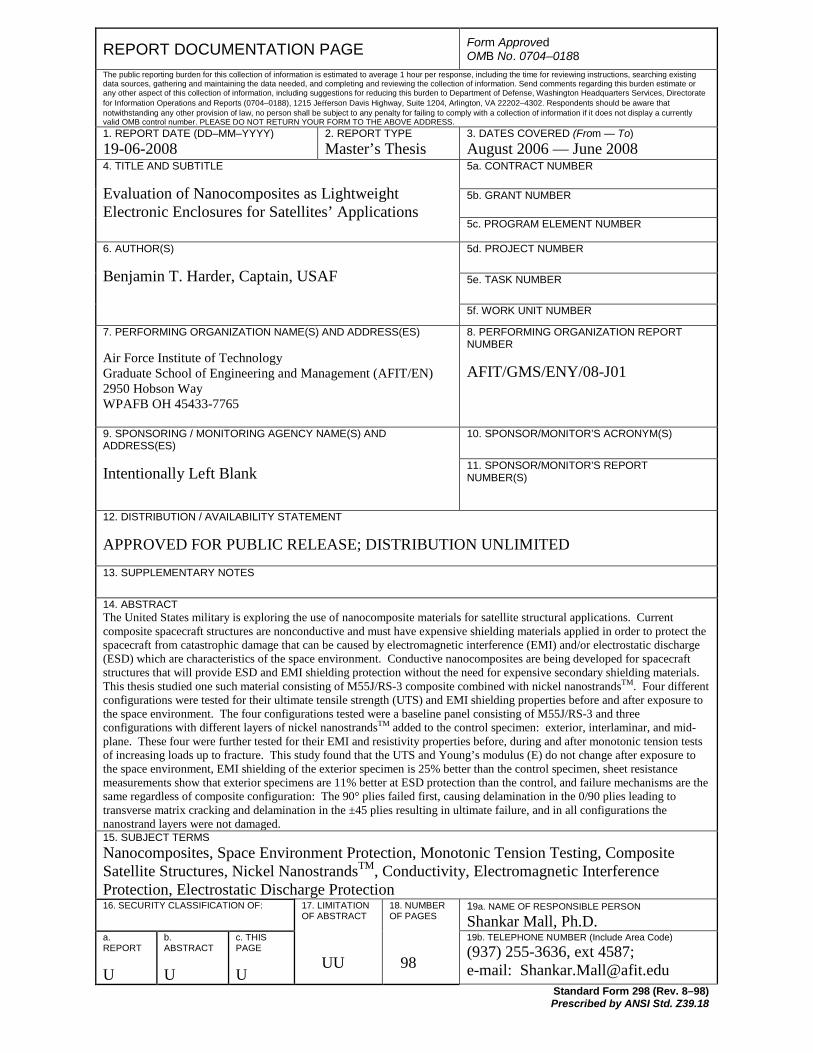
REPORT DOCUMENTATION PAGE Form Approved OMB No. 0704–0188
The public reporting burden for this collection of information is estimated to average 1 hour per response, including the time for reviewing instructions, searching existing data sources, gathering and maintaining the data needed, and completing and reviewing the collection of information. Send comments regarding this burden estimate or any other aspect of this collection of information, including suggestions for reducing this burden to Department of Defense, Washington Headquarters Services, Directorate for Information Operations and Reports (0704–0188), 1215 Jefferson Davis Highway, Suite 1204, Arlington, VA 22202–4302. Respondents should be aware that notwithstanding any other provision of law, no person shall be subject to any penalty for failing to comply with a collection of information if it does not display a currently valid OMB control number. PLEASE DO NOT RETURN YOUR FORM TO THE ABOVE ADDRESS. 1. REPORT DATE (DD–MM–YYYY) 19-06-2008
2. REPORT TYPE Master’s Thesis
3. DATES COVERED (From — To) August 2006 — June 2008
4. TITLE AND SUBTITLE Evaluation of Nanocomposites as Lightweight Electronic Enclosures for Satellites’ Applications
5a. CONTRACT NUMBER
5b. GRANT NUMBER
5c. PROGRAM ELEMENT NUMBER
6. AUTHOR(S) Benjamin T. Harder, Captain, USAF
5d. PROJECT NUMBER
5e. TASK NUMBER
5f. WORK UNIT NUMBER
7. PERFORMING ORGANIZATION NAME(S) AND ADDRESS(ES) Air Force Institute of Technology Graduate School of Engineering and Management (AFIT/EN) 2950 Hobson Way WPAFB OH 45433-7765
8. PERFORMING ORGANIZATION REPORT NUMBER AFIT/GMS/ENY/08-J01
9. SPONSORING / MONITORING AGENCY NAME(S) AND ADDRESS(ES) Intentionally Left Blank
10. SPONSOR/MONITOR’S ACRONYM(S)
11. SPONSOR/MONITOR’S REPORT NUMBER(S)
12. DISTRIBUTION / AVAILABILITY STATEMENT APPROVED FOR PUBLIC RELEASE; DISTRIBUTION UNLIMITED
13. SUPPLEMENTARY NOTES
14. ABSTRACT The United States military is exploring the use of nanocomposite materials for satellite structural applications. Current composite spacecraft structures are nonconductive and must have expensive shielding materials applied in order to protect the spacecraft from catastrophic damage that can be caused by electromagnetic interference (EMI) and/or electrostatic discharge (ESD) which are characteristics of the space environment. Conductive nanocomposites are being developed for spacecraft structures that will provide ESD and EMI shielding protection without the need for expensive secondary shielding materials. This thesis studied one such material consisting of M55J/RS-3 composite combined with nickel nanostrandsTM. Four different configurations were tested for their ultimate tensile strength (UTS) and EMI shielding properties before and after exposure to the space environment. The four configurations tested were a baseline panel consisting of M55J/RS-3 and three configurations with different layers of nickel nanostrandsTM added to the control specimen: exterior, interlaminar, and mid-plane. These four were further tested for their EMI and resistivity properties before, during and after monotonic tension tests of increasing loads up to fracture. This study found that the UTS and Young’s modulus (E) do not change after exposure to the space environment, EMI shielding of the exterior specimen is 25% better than the control specimen, sheet resistance measurements show that exterior specimens are 11% better at ESD protection than the control, and failure mechanisms are the same regardless of composite configuration: The 90° plies failed first, causing delamination in the 0/90 plies leading to transverse matrix cracking and delamination in the ±45 plies resulting in ultimate failure, and in all configurations the nanostrand layers were not damaged. 15. SUBJECT TERMS Nanocomposites, Space Environment Protection, Monotonic Tension Testing, Composite Satellite Structures, Nickel NanostrandsTM, Conductivity, Electromagnetic Interference Protection, Electrostatic Discharge Protection 16. SECURITY CLASSIFICATION OF: 17. LIMITATION
OF ABSTRACT
UU
18. NUMBER OF PAGES
98
19a. NAME OF RESPONSIBLE PERSON Shankar Mall, Ph.D.
a. REPORT U
b. ABSTRACT U
c. THIS PAGE U
19b. TELEPHONE NUMBER (Include Area Code)
(937) 255-3636, ext 4587; e-mail: [email protected]
Standard Form 298 (Rev. 8–98) Prescribed by ANSI Std. Z39.18