Embed Size (px)
Citation preview

273FUJITSU Sci. Tech. J., Vol. 46, No. 3, pp. 273–279 (July 2010)
Evaluation of Devices and Materials by Transmission Electron Microscopy
Toyoo Miyajima Ryoji Ito Koichiro Honda Mineharu Tsukada(Manuscript received December 28, 2009)
With the components of cutting-edge devices becoming smaller and more complicated and their constituent materials becoming more multilayered and diversified, nanometer-order structural control has recently become indispensable. To improve the performance and reliability of manufactured products like these devices, nanometer-order evaluation technology is therefore essential. As examples, this paper introduces four techniques for materials and device analysis that utilize transmission electron microscopy (TEM): three-dimensional observation by electron tomography for evaluating device features controlled at the nanometer-level, electron holography for visualizing information about the electric and magnetic fields of devices at the nanometer-level, high-resolution TEM observation and electron-energy-loss spectroscopy for analyzing the crystal structure and composition of nanostructure multilayers, and high-angle annular dark-field scanning transmission electron microscopy for observing the atomic arrangement of ordered alloys and analyzing heteroepitaxial interface structures.
1. IntroductionIn the development of manufactured
products like devices, the merging of optimal design and process development with the development of constituent materials is enabling the production of products with high reliability and performance at commercial production yields. With the components of cutting-edge devices becoming smaller and more complex and their materials becoming more multilayered and diversified, nanometer-order evaluation techniques have recently become necessary. In response to these circumstances, we are applying transmission electron microscopy (TEM), which has high spatial resolution, as a nanometer-order evaluation technique for evaluating materials and devices.
A transmission electron microscope forms images by irradiating a thin sample with an electron beam that is focused by an
electromagnetic lens and passes through the sample. The wavelength of the electrons in typical TEM (beam-acceleration voltage: 200 kV) is 0.0025 nm, which provides spatial resolution about 0.1 nm. Furthermore, if we visualize the electric and magnetic fields of samples (by utilizing the electron wave interference characteristics) combined with high-spatial-resolution imaging and utilize characteristic X-rays and electron energy loss generated by the interaction between electrons and materials, TEM can analyze local atomic species and chemical-bonding conditions in samples. Consequently, by utilizing these characteristics of TEM, we can evaluate devices and materials from various aspects.
In this paper, as examples of TEM analysis of materials and devices, we describe four techniques: three-dimensional (3D) observation of device structures by electron tomography, visualization of electric and magnetic fields by
274 FUJITSU Sci. Tech. J., Vol. 46, No. 3 (July 2010)
T. Miyajima et al.: Evaluation of Devices and Materials by Transmission Electron Microscopy
electron holography, analysis of nanostructure multilayers by high-resolution TEM (HRTEM) observation and electron energy-loss spectroscopy (EELS), and evaluation of heteroepitaxial-interface structures by high-angle annular dark-field scanning transmission electron microscopy (HAADF STEM).
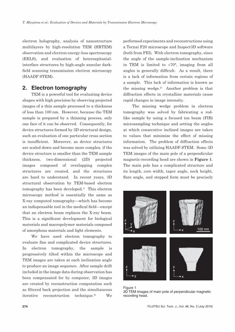
2. Electron tomographyTEM is a powerful tool for evaluating device
shapes with high precision by observing projected images of a thin sample processed to a thickness of less than 100 nm. However, because the TEM sample is prepared by a thinning process, only one face of it can be observed. Consequently, for device structures formed by 3D structural design, such an evaluation of one particular cross section is insufficient. Moreover, as device structures are scaled down and become more complex, if the device structure is smaller than the TEM sample thickness, two-dimensional (2D) projected images composed of overlapping complex structures are created, and the structures are hard to understand. In recent years, 3D structural observation by TEM-based electron tomography has been developed.1) This electron microscopy method is essentially the same as X-ray computed tomography—which has become an indispensable tool in the medical field—except that an electron beam replaces the X-ray beam. This is a significant development for biological materials and macropolymer materials composed of amorphous materials and light elements.
We have used electron tomography to evaluate fine and complicated device structures. In electron tomography, the sample is progressively tilted within the microscope and TEM images are taken at each inclination angle to produce an image sequence. After sample drift included in the image data during observation has been compensated for by computer, 3D images are created by reconstruction computation such as filtered back projection and the simultaneous iterative reconstruction technique.2) We
performed experiments and reconstructions using a Tecnai F20 microscope and Inspect3D software (both from FEI). With electron tomography, since the angle of the sample-inclination mechanism in TEM is limited to ±70°, imaging from all angles is generally difficult. As a result, there is a lack of information from certain regions of a sample. This lack of information is known as the missing wedge.2) Another problem is that diffraction effects in crystalline materials cause rapid changes in image intensity.
The missing wedge problem in electron tomography was solved by fabricating a rod-like sample by using a focused ion beam (FIB) microsampling technique and setting the angles at which consecutive inclined images are taken to values that minimize the effect of missing information. The problem of diffraction effects was solved by utilizing HAADF-STEM. Some 3D TEM images of the main pole of a perpendicular magnetic-recording head are shown in Figure 1. The main pole has a complicated structure and its length, core width, taper angle, neck height, flare angle, and stepped form must be precisely
x
yz
x
z
x
y
y
z
100 nm
Figure 13D TEM images of main pole of perpendicular magnetic recording head.

275FUJITSU Sci. Tech. J., Vol. 46, No. 3 (July 2010)
T. Miyajima et al.: Evaluation of Devices and Materials by Transmission Electron Microscopy
controlled. Deviations in any of these parameters affect the other parameters. Observation with 3D TEM images lets one understand complicated component configurations in three dimensions. Moreover, by extracting arbitrary cross sections, one can measure each of the main pole parameters.
3. Electron holographyAn electron wave transmitted through a
sample (object wave) generates a phase change due to electric and magnetic fields in the sample, and the phase is advanced by another wave (reference wave) propagating in a vacuum. However, a normal TEM image records only the intensity of electron wave: it does not directly represent phase information. On the other hand, electron holography,3) which overlaps the object wave and the reference wave, records the phase change in an interference pattern called a hologram. In TEM-based electron holography, interference between the object and reference waves is achieved by using an electron biprism set in the selected area aperture position, and a hologram is recorded by a charge-coupled device (CCD) camera. The phase-reconstructed image is obtained from the hologram by Fourier transforming the hologram, shifting it to the point of origin by applying a spatial-frequency filter to one side-band, and inverse Fourier
transforming it. We performed experiments and reconstructions using a Tecnai F20 microscope and HoloWorks software (GATAN).
As an example of the evaluation of the magnetic field of a device, the spatial distribution of the magnetic field generated by the write head of a magnetic recording head is shown in Figure 2. For this measurement, a magnetic recording head (shaped as a rectangular-body slider with dimensions of 0.85 × 0.70 × 0.23 mm3) was fixed in a TEM specimen holder, and direct current from the write head’s coil terminal was applied. As a result, the magnetic field from the write head spread into the vacuum. Its distribution around the upper magnetic pole, write gap, and lower magnetic pole is visualized.
As an example showing an evaluated electric field, a silicon semiconductor p-n junction is shown in Figure 3. The sample was prepared by FIB to a uniform thickness of 250 nm. To minimize the dynamical diffraction effect, the measurement was performed with the electron beam incidence direction inclined 4° from the [110] direction of the silicon (Si) substrate. Moreover, to enable accurate measurement of the phase change due
5 m
Coil
Lower magnetic pole
Upper magnetic pole
Write gap
200 nm
Polycrystalline Si
np
n
(a) TEM image
(b) Reconstructed phase image
Si substrate
200 nm
Figure 2Spatial distribution of magnetic field generated from magnetic recording head.
Figure 3p-n junction of silicon semiconductor device.
276 FUJITSU Sci. Tech. J., Vol. 46, No. 3 (July 2010)
T. Miyajima et al.: Evaluation of Devices and Materials by Transmission Electron Microscopy
to the weak electric field, a reference hologram was measured and Fresnel fringes generated by an electron biprism and distortions caused by the many sources of equipment were removed. Although the p-n junction cannot be seen in the TEM image in Figure 3 (a), it can be seen clearly in the reconstructed phase image in Figure 3 (b).
4. Evaluation of nanostructure multilayersAs an example of a nanometer-order
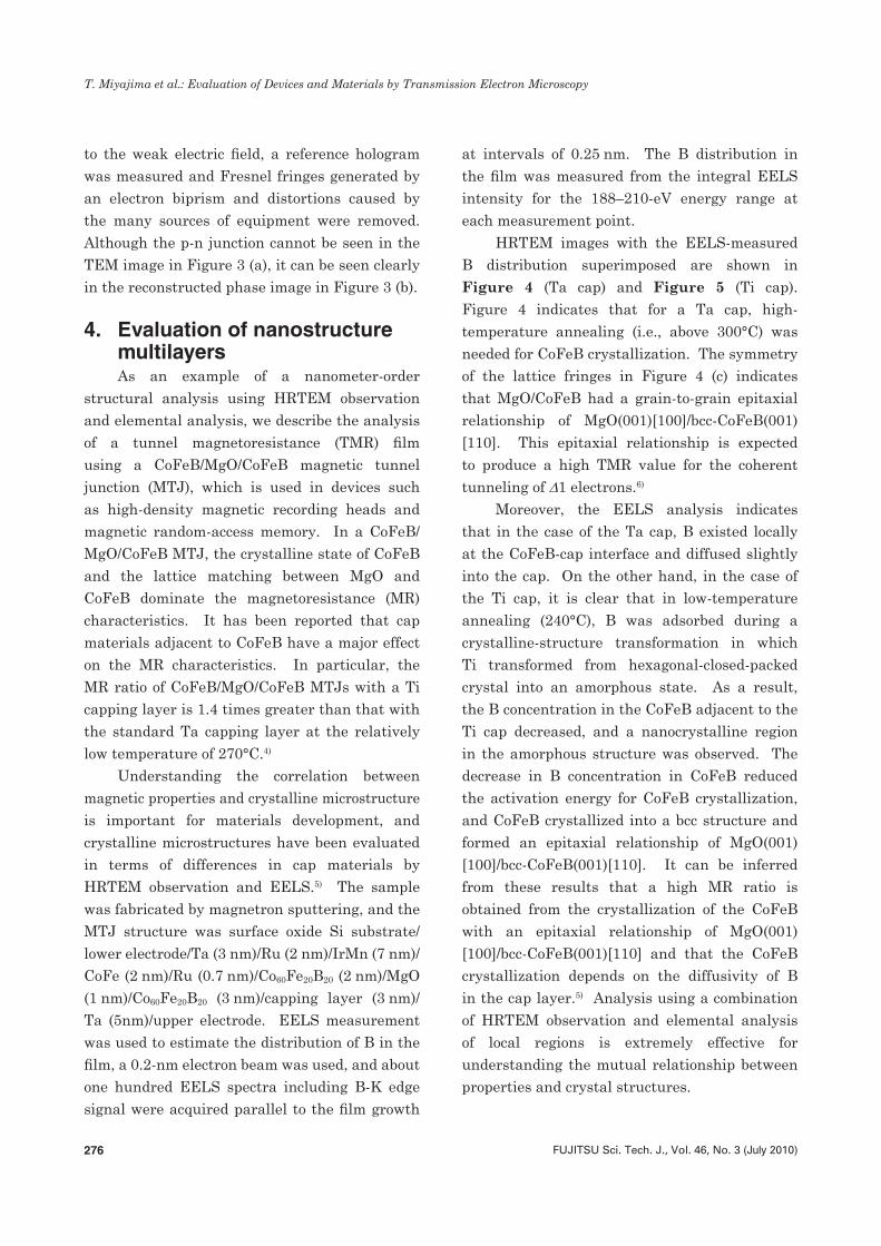
structural analysis using HRTEM observation and elemental analysis, we describe the analysis of a tunnel magnetoresistance (TMR) film using a CoFeB/MgO/CoFeB magnetic tunnel junction (MTJ), which is used in devices such as high-density magnetic recording heads and magnetic random-access memory. In a CoFeB/MgO/CoFeB MTJ, the crystalline state of CoFeB and the lattice matching between MgO and CoFeB dominate the magnetoresistance (MR) characteristics. It has been reported that cap materials adjacent to CoFeB have a major effect on the MR characteristics. In particular, the MR ratio of CoFeB/MgO/CoFeB MTJs with a Ti capping layer is 1.4 times greater than that with the standard Ta capping layer at the relatively low temperature of 270°C.4)
Understanding the correlation between magnetic properties and crystalline microstructure is important for materials development, and crystalline microstructures have been evaluated in terms of differences in cap materials by HRTEM observation and EELS.5) The sample was fabricated by magnetron sputtering, and the MTJ structure was surface oxide Si substrate/lower electrode/Ta (3 nm)/Ru (2 nm)/IrMn (7 nm)/ CoFe (2 nm)/Ru (0.7 nm)/Co60Fe20B20 (2 nm)/MgO (1 nm)/Co60Fe20B20 (3 nm)/capping layer (3 nm)/Ta (5nm)/upper electrode. EELS measurement was used to estimate the distribution of B in the film, a 0.2-nm electron beam was used, and about one hundred EELS spectra including B-K edge signal were acquired parallel to the film growth
at intervals of 0.25 nm. The B distribution in the film was measured from the integral EELS intensity for the 188–210-eV energy range at each measurement point.
HRTEM images with the EELS-measured B distribution superimposed are shown in Figure 4 (Ta cap) and Figure 5 (Ti cap). Figure 4 indicates that for a Ta cap, high-temperature annealing (i.e., above 300°C) was needed for CoFeB crystallization. The symmetry of the lattice fringes in Figure 4 (c) indicates that MgO/CoFeB had a grain-to-grain epitaxial relationship of MgO(001)[100]/bcc-CoFeB(001)[110]. This epitaxial relationship is expected to produce a high TMR value for the coherent tunneling of ∆1 electrons.6)
Moreover, the EELS analysis indicates that in the case of the Ta cap, B existed locally at the CoFeB-cap interface and diffused slightly into the cap. On the other hand, in the case of the Ti cap, it is clear that in low-temperature annealing (240°C), B was adsorbed during a crystalline-structure transformation in which Ti transformed from hexagonal-closed-packed crystal into an amorphous state. As a result, the B concentration in the CoFeB adjacent to the Ti cap decreased, and a nanocrystalline region in the amorphous structure was observed. The decrease in B concentration in CoFeB reduced the activation energy for CoFeB crystallization, and CoFeB crystallized into a bcc structure and formed an epitaxial relationship of MgO(001)[100]/bcc-CoFeB(001)[110]. It can be inferred from these results that a high MR ratio is obtained from the crystallization of the CoFeB with an epitaxial relationship of MgO(001)[100]/bcc-CoFeB(001)[110] and that the CoFeB crystallization depends on the diffusivity of B in the cap layer.5) Analysis using a combination of HRTEM observation and elemental analysis of local regions is extremely effective for understanding the mutual relationship between properties and crystal structures.

277FUJITSU Sci. Tech. J., Vol. 46, No. 3 (July 2010)
T. Miyajima et al.: Evaluation of Devices and Materials by Transmission Electron Microscopy
5. Evaluation of heteroepitaxial interfacesHAADF STEM provides incoherent images
and atomic number (Z) contrast images. Unlike the coherent images of conventional HRTEM, HAADF STEM images do not suffer from problems related to the Fresnel effect at the interface and defocus dependence. Therefore, HAADF STEM is an effective method for directly observing crystal structures and interfacial structures.7) An electron microscope with spherical aberration
correction has recently achieved a high-intensity convergent electron beam with a diameter of around 0.1 nm, and atomic-resolution HAADF STEM observation is becoming possible.8) As an example of material evaluation using HAADF STEM, we describe a heteroepitaxial interface structure of an ordered alloy and an oxide film.
The sample was Co2MnSi/MgO/Co2MnSi MTJ deposited on a MgO substrate. Co2MnSi is an intermetallic compound exhibiting half-metallicity. If an ideal half-metallic material
IrMn
CoFe
Ru
CoFeB
MgO
CoFeB
Ta
(002)
Amorphous
IrMn
CoFe
Ru
CoFeB
MgO
CoFeB
Ta
5 nmB count (arb.units)
(002)(002)
Amorphous
(002)
(002)
bcc crystal
(002)
(002)(002)
AmorphousAmorphous
(a) Before annealing (b) After annealing at 270ºC�� (c) After annealing at 320ºC
bcc crystal
Figure 4HRTEM images (with B distribution superimposed) of CoFeB/MgO/CoFeB MTJ with Ta cap.
IrMnCoFe
Ru
CoFeB
MgO
CoFeB
(002) (002)
Nanocrystalline
(002)
(002)Amorphous
Amorphous Ti
IrMnCoFe
Ru
CoFeB
MgO
CoFeB
TaTa
TiTi(1010)(1010)
(002) (002)
Nanocrystalline
(002)
(002)Amorphous
5 nmB count (arb.units)
(a) Before annealing (b) After annealing at 240ºC� (c) After annealing at 270ºC
hcp-Ti Amorphous Ti Amorphous Ti
Figure 5HRTEM images (with B distribution superimposed) of CoFeB/MgO/CoFeB MTJ with Ti cap.
278 FUJITSU Sci. Tech. J., Vol. 46, No. 3 (July 2010)
T. Miyajima et al.: Evaluation of Devices and Materials by Transmission Electron Microscopy
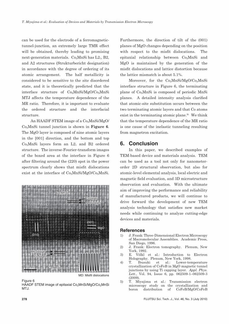
can be used for the electrode of a ferromagnetic-tunnel-junction, an extremely large TMR effect will be obtained, thereby leading to promising next-generation materials. Co2MnSi has L21, B2, and A2 structures (Strukturbericht designation) in accordance with the degree of ordering of its atomic arrangement. The half metallicity is considered to be sensitive to the site disordered state, and it is theoretically predicted that the interface structure of Co2MnSi/MgO/Co2MnSi MTJ affects the temperature dependence of the MR ratio. Therefore, it is important to evaluate the ordered structure and the interfacial structure.
An HAADF STEM image of a Co2MnSi/MgO/Co2MnSi tunnel junction is shown in Figure 6. The MgO layer is composed of nine atomic layers in the [001] direction, and the bottom and top Co2MnSi layers form an L21 and B2 ordered structure. The inverse-Fourier-transform images of the boxed area at the interface in Figure 6 after filtering around the (220) spot in the power spectrum clearly shows that misfit dislocations exist at the interface of Co2MnSi/MgO/Co2MnSi.
Furthermore, the direction of tilt of the (001) planes of MgO changes depending on the position with respect to the misfit dislocations. The epitaxial relationship between Co2MnSi and MgO is maintained by the generation of the misfit dislocations and lattice distortion because the lattice mismatch is about 5.1%.
Moreover, for the Co2MnSi/MgO/Co2MnSi interface structure in Figure 6, the terminating plane of Co2MnSi is composed of periodic MnSi planes. A detailed intensity analysis clarified that atomic-site substitution occurs between the two terminating atomic layers and that Co atoms exist in the terminating atomic plane.9) We think that the temperature dependence of the MR ratio is one cause of the inelastic tunneling resulting from magnetron excitation.
6. ConclusionIn this paper, we described examples of
TEM-based device and materials analysis. TEM can be used as a tool not only for nanometer-order 2D structural observation, but also for atomic-level elemental analysis, local electric and magnetic field evaluation, and 3D microstructure observation and evaluation. With the ultimate aim of improving the performance and reliability of manufactured products, we will continue to drive forward the development of new TEM analysis technology that satisfies new market needs while continuing to analyze cutting-edge devices and materials.
References1) J. Frank: Three-Dimensional Electron Microscopy
of Macromolecular Assemblies. Academic Press, San Diego, 1996.
2) J. Frank: Electron tomography. Plenum, New York, 1992.
3) E. Völkl et al.: Introduction to Electron Holography. Plenum, New York, 1998.
4) T. Ibusuki et al.: Lower-temperature crystallization of CoFeB in MgO magnetic tunnel junctions by using Ti capping layer. Appl. Phys. Lett., Vol. 94, Issue 6, pp. 062509-1–062509-3 (2009).
5) T. Miyajima et al.: Transmission electron microscopy study on the crystallization and boron distribution of CoFeB/MgO/CoFeB
MgO
Co layer
MnSi layer
1 nm Co2MnSi
Co layer
MnSi layer
Co layerMnSi layer
Co2MnSi
Co layerMnSi layer
(001)
(010)
1 nm
Co2MnSi
Co2MnSi
MDMD
MD: Misfit dislocations
Figure 6HAADF STEM image of epitaxial Co2MnSi/MgO/Co2MnSi MTJ.

279FUJITSU Sci. Tech. J., Vol. 46, No. 3 (July 2010)
T. Miyajima et al.: Evaluation of Devices and Materials by Transmission Electron Microscopy
magnetic tunnel junctions with various capping layers. Appl. Phys. Lett., Vol. 94, Issue 12, pp. 122501-1–122501-3 (2009).
6) W. H. Butler et al.: Spin-dependent tunneling conductance of Fe|MgO|Fe sandwiches. Phys. Rev., B, Vol. 63. Issue 5, pp. 054416-1–054416-12 (2001).
7) S. J. Pennycook et al.: Impact of Electron and Scanning Probe Microscopy on Material Research. Kluwer, Dordrecht, 1999.
8) Y. Kotaka et al.: Atomic-Resolution Imaging and Analysis with Cs-Correlated Scanning Transmission Electron Microscopy. FUJITSU Sci. Tech. J., Vol. 46, No. 3, pp. 249–256 (2010).
9) T. Miyajima et al.: Direct observation of atomic ordering and interface structure in Co2MnSi/MgO/Co2MnSi magnetic tunnel junctions by high-angle annular dark-field scanning transmission electron microscopy. Appl. Phys. Express, Vol. 2, No. 9, pp. 093001-1–093001-3 (2009).
Toyoo MiyajimaFujitsu Laboratories Ltd.Mr. Miyajima received B.S. and M.S. degrees in Applied Physics from Tohoku University, Sendai, Japan in 1994 and 1996, respectively. He joined Fujitsu Laboratories Ltd., Atsugi, Japan in 1996 and has been engaged in research and development of materials and device characterization by transmission electron microscopy. He is a member of the Magnetic Society of Japan.
Ryoji ItoFujitsu Laboratories Ltd.Mr. Ito received a B.S. degree in Physics and an M.S. degree in Condensed Matter Physics from Tokyo Institute of Technology, Japan in 2003 and 2005, respectively. He joined Fujitsu Laboratories Ltd., Atsugi, Japan in 2005 and has been engaged in research and development of materials and device analysis by transmission
electron microscopy. He is currently researching and developing environmental technology and devices.
Mineharu TsukadaFujitsu Laboratories Ltd.Dr. Tsukada received B.S. and M.S. degrees in Metallurgical Engineering from Waseda University, Tokyo, Japan in 1982 and 1984, respectively. He received a Ph.D. degree in Materials Engineering from Tokyo Institute of Technology, Japan in 2004. He joined Fujitsu Laboratories Ltd., Atsugi, Japan in 1984 and has been engaged in
research and development of electronic materials and devices. He is a member of the Ceramics Society of Japan, Japan Society of Applied Physics, and Surface Science Society of Japan.
Koichiro HondaFujitsu Laboratories Ltd.Dr. Honda received a D.Eng. degree from Tokyo Institute of Technology in 1995. He joined Fujitsu Laboratories Ltd., Kawasaki, Japan in 1977 and engaged in research and development of Si crystals, ferroelectric materials for ICs, and memory devices. He has also been developing methods for determining the characteristics of
materials and devices using transmission electron microscopy and scanning probe microscopy. He is a part-time lecturer at the Technology School of Hosei University and a guest professor at the Research Institute of Electrical Communication, Tohoku University. He is a member of the Materials Research Society.