Embed Size (px)
Citation preview

EUV resist: the great challenge of small thingsS. CastellanosEUVL Workshop 11-14 June 2018, Berkeley

“Looking ahead towards second-generation EUV
lithography, resist stochastic effects are definitely one of the
top concerns.” Harry Levinson, Global Foundries
(Semiconductor Engineering, March 2018)
“The current resists may not take us into the future. Novel
ideas and approaches for stochastics are needed.” Anna Lio,
Intel (Proc. SPIE, 2016)
”New resists/chemistries are needed for next generation EUV.”
Anindarupa Chunder, Global Foundries (IEUVLI TWG Meeting,
2018)
”Readiness of commercial resists will be a leading challenge
for EUVL in future nodes.” Vivek Bakshi, EUV Litho Inc.
(EET Asia, February 2018)
Motivation
”What we would describe as challenge number one in imaging is in the
extreme roughness events or the stochastic failures in places like nano-
bridging, line breaking and merging or missing holes.” Gregory McIntyre,
Imec (Semiconductor Engineering, September 2017)
• (secondary electrons)
Can we define common targets and goals in a roadmap for the whole EUV resists community?
Unlike the case of the EUV scanner, there are multiple parties working on resists but no general consensus.

• Historic trends of EUV resists• What do we know about mechanisms in EUV resists?• What do we not know about EUV resists?
Table of contents
• What is needed from photoresists?
• Where are we?
• How are we going to make resists ready?

• Historic trends of EUV resists• What do we know about mechanisms in EUV resists?• What do we not know about EUV resists?
Table of contents
• What is needed from photoresists?
• Where are we?
• How are we going to make resists ready?

0
0.5
1
1.5
2
2.5
3
3.5
4
4.5
5
0
2
4
6
8
10
12
14
16
18
20
2016 2018 2020 2022 2024 2026 2028 2030
LER
(3s
) /
nm
Ha
lf P
itch
/ n
m
Line/space roadmap in literature
Where are we?
”10”
”7”
”5”
”3”
”2.1” ”1.5”
O. Yildirim, Proc. SPIE 2017; D. de Simone, Proc. SPIE 2018; ITRS, http://www.itrs2.net/2013-itrs.html; IRDS 2017

Requirements according to literature
Dose (mJ/cm2) m (mm-1) LWR 3s(nm)
LER 3s (nm) PSD(0) defectivity
<20[1,2,3,4] 15*[5] < 20%[4] < 12-15% CD[2,3,]
??? pixNOK (space) = 10-5[5]
VIA failure < 10-12[1]
Some of best reported performances
CAR (CD = 16 nm)[6]
45 5 2.91 2.01 pixNOK <D.L. (10-7)
CAR(CD = 13 nm)[2]
58 5 4.4
nCAR(CD = 16 nm)[2]
47.5 20 4.0
nCAR(CD = 13 nm)[2]
34 20 3.8
PSCAR[7] 37.5 (15 J/cm2 UV) 1.94 25.7
IM[8] 38.5 3.7
not specified[4] 21.4 5.2
[1] A. Lio Proc. SPIE 2016, 97760V; [2] O. Yildirim, Proc. SPIE 2017, 101430Q; [3] ITRS 2013; [4] De Simone, J. Photopolym. Sci. Technol 2017; [5] A. Chunder, IEUVI resists TWG 2018; [6] De Simone Proc. SPIE 2018, 105830G; [7] S. Nagahara Proc. SPIE 2018, 1058606; [8] Y. Vesters, Proc. SPIE 2018, 1058308; G. Denbeaux IEUVI resists TWG 2018
* Calculated for the requirement of OD = 36% in a 30 nm photoresist

0
0.5
1
1.5
2
2.5
3
3.5
4
4.5
5
0
2
4
6
8
10
12
14
16
18
20
2016 2018 2020 2022 2024 2026 2028 2030
LER
(3s
) /
nm
Ha
lf P
itch
/ n
m
Line/space roadmap in literature
Where are we?
”10”
”7”
”5”
”3”
”2.1” ”1.5”

Requirements according to literature
Dose (mJ/cm2) m (mm-1) LWR 3s(nm)
LER 3s (nm) PSD(0) defectivity
<20[1,2,3,4] 15*[5] < 20%[4] < 12-15% CD[2,3,]
??? pixNOK (space) = 10-5[5]
VIA failure < 10-12[1]
Some of best reported performances
CAR (CD = 16 nm)[6]
45 5 2.91 2.01 pixNOK <D.L. (10-7)
CAR(CD = 13 nm)[2]
58 5 4.4
nCAR(CD = 16 nm)[2]
47.5 20 4.0
nCAR(CD = 13 nm)[2]
34 20 3.8
PSCAR[7] 37.5 (15 J/cm2 UV) 1.94 25.7
IM[8] 38.5 3.7
not specified[4] 21.4 5.2
[1] A. Lio Proc. SPIE 2016, 97760V; [2] O. Yildirim, Proc. SPIE 2017, 101430Q; [3] ITRS 2013; [4] De Simone, J. Photopolym. Sci. Technol 2017; [5] A. Chunder, IEUVI resists TWG 2018; [6] De Simone Proc. SPIE 2018, 105830G; [7] S. Nagahara Proc. SPIE 2018, 1058606; [8] Y. Vesters, Proc. SPIE 2018, 1058308; G. Denbeaux IEUVI resists TWG 2018
* Calculated for the requirement of OD = 36% in a 30 nm photoresist
• (secondary electrons) Defectivity decreases with absorptivity!![5,9]

PSD(0)
1
2𝜋𝜉
white noise, uncorrelated events correlated events (resist chemistry related)
What is needed from EUV resists?
It is not only about decreasing 3s
Chris A. Mack, IEUVI Resist TWG meeting, Feb. 25 2018

• Historic trends of EUV resists• What do we know about mechanisms in EUV resists?• What do we not know about EUV resists?
Table of contents
• What is needed from photoresists?
• Where are we?
• How are we going to make photoresists ready?

Historic trends
First tests with 11 nm in 1986 on PMMA by Kinoshita
Namioka, Revue Phys. Appl. 1998, 23, 1711-1726

Historic trends
Required Actual
P. Naulleau, Frontiers Nanoscience 2016

What do we know?
Non-chemically amplified inorganic resists (nCAR)
e- cascade induced reaction H+ catalysis
Chemically amplified resists (CAR)
e- cascade induced reaction

Nanoparticles:• Ober+ High sensitivity (<3 mJ/cm2 - High LER• Inpria (peroxide HfOx)+ High sensitivity
CAR
PSCAR• More sensitive• Improved contrast in latent image
New formulations:• Enhanced absorptivity• Decreased acid diffusion
▪ Covalently bonded PGA▪ Higher Tg (JSR)
Molecular based:• Well defined structure => LER• Tuneability
Multitrigger (Irresistible materials)• Improved contrast in latent image
Sn-based Inpria molecular materials:+High absorptivity (20 mm-1)∼ Sensitivity
nCAR
Too dynamic bonding??
Ligand loss not efficient enough?
MORE (Brainard):• Sn-based + low LER (2.1 nm CD = 16 nm)- 600 mJ/cm2
• Other metals+ High sensitivity (5.6 mJ/cm2, 35 nm Pitch)
MOCs (Castellanos, Ober)+ Sensitivity tuned by metal content- LER scumming
What do we know?
General concerns: • absorption of EUV photons• resolving low CDs
Chem. Soc. Rev., 2017, 46,4855
What do we know?
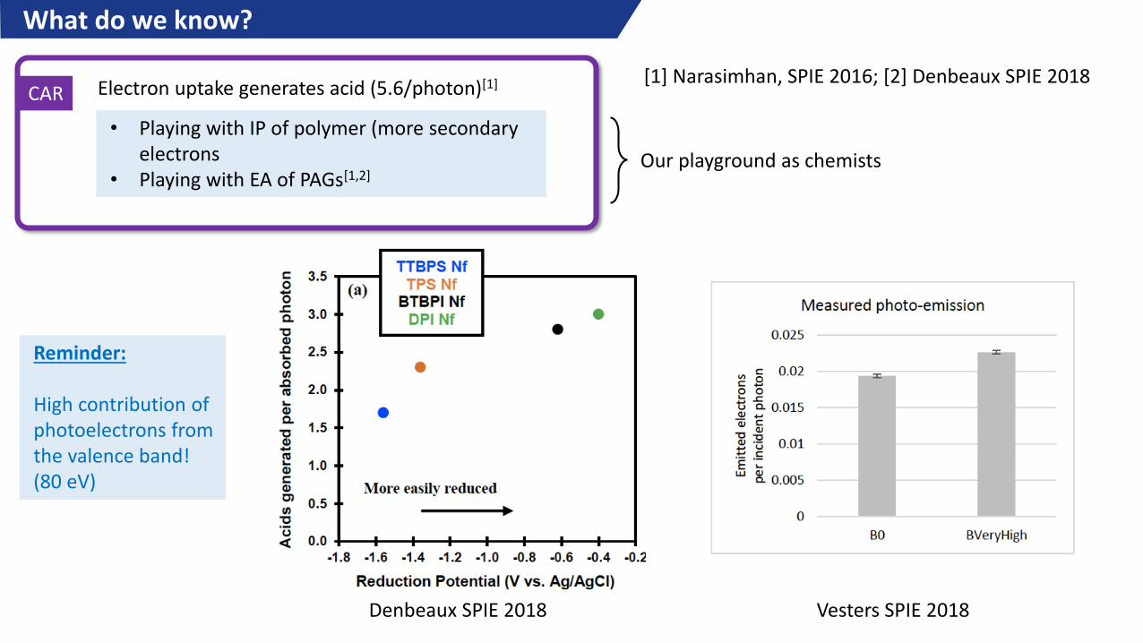
Electron uptake generates acid (5.6/photon)[1]
Our playground as chemists
CAR[1] Narasimhan, SPIE 2016; [2] Denbeaux SPIE 2018
• Playing with IP of polymer (more secondary electrons
• Playing with EA of PAGs[1,2]
Denbeaux SPIE 2018 Vesters SPIE 2018
Reminder:
High contribution of photoelectrons from the valence band! (80 eV)

PSCAR®
Proc. of SPIE 2018, 10583, 1058308
Proc. of SPIE (2016), 9776, 977607
Irresistible Materials®
What do we know?

What do we know?
De Simone, J. Photopolym. Sci. Technol. 2017, 30, 613
• At 5 nm CARs fail too much[1]
• At lower node CARs cannot operate[1]
• Chemical stochastics in the range of photons stochastics[2]
Main issues
• Roughness (PSD)• Defectivity (NOK)
[1] A. Vaglio Pret, SPIE 2017; [2] Naulleau Frontiers of Nanoscience
Claims

Ligand cleavage + aggregation
Ligand cleavage + aggregation Ligand exchange: polarity
Hinsberg SPIE 2017
What do we know?
• Inorganic core defines the absorption and photoelectron yield
• Organic shell defines the type of chemistry and the secondary electron yield
work in progress in ARCNL:-> absorption tuning with metal-> promoting electron-induced cleavage in ligands-> low ionization potential
Castellanos SPIE 2018 Ober Newsroom SPIE 2014

Where are we?
Can we find some guidelines with so many variables??
…well, there are some features in common

• Historic trends of EUV resists• What do we know about mechanisms in EUV resists?• What do we not know about EUV resists?
Table of contents
• What is needed from photoresists?
• Where are we?
• How are we going to make photoresists ready?

What we do not know?
Some personal thoughts• Electrons above IP generates electrons• Electrons below IP interact resonantly with the molecules => need of potential curves• Contribution of holes??
W. Van Dorp Frontiers Nanoscience 2016

AFM
295290275 280 285
Photon Energy [eV]Ire
f. /Iexp
. [a.u
.]
NEXAFS
C-K
Edge
Without exposure
283.3 285.7
Photon Energy [eV]
Iref. /Ie
xp
. [a.u
.]
500485 490 495
NEXAFS
Sn-M EdgeWithout exposure
488.9 497.2
493.1
• (secondary electrons) Currently at ARCNL: chemistry of secondary electrons
What we do not know?

• (secondary electrons)
Increase solubility contrast/sensitivityDecrease of defects
• Absorption• Photoelectron yield• More effective chemistry (hole, electron
induced)• Play with underlayer
• (secondary electrons) Study of low energy electrons:• Cross-sections for specific reactions• Secondary electrons per photoelectron [Thete, 2017 PRL]• Mean free paths
Gain fundamental knowledge
Photoelectron yield (Auger, valence) [Ogletree]
Improvement on current systems
• (secondary electrons)
Breakthrough!!
• Use the knowledge on:▪ Photoelectrons yield▪ Secondary electrons▪ Electron and hole chemistry
for new concepts.
202020192018
• (secondary electrons)
HP = 7nm!!

• (secondary electrons)
• (secondary electrons)
• (secondary electrons)
• (secondary electrons)
▪ Layer of dense and ordered metal absorbers▪ Use of hot electrons to do chemistry on resist
• Propagation of the image only perpendicular to the plane (less shot noise)
▪ Smaller and more dense units: metal halogens?▪ Rule out muliple components with random distribution: CAR, ligand exchange
New concepts
• Thin film resists with high etching resistance:• Promoting a change in the oxidation state of the underlayer to switch etching resistance
Simplify systems
Separating absorption and chemical events
”Transforming” high energy electrons in low energy electrons
Introducing anisotropy
▪ Avoid development? (volatile inert products?)
• Electron scattering through layer that yields plasmons/hot electrons
(*similar idea by AZ Electronic Materials Manufacturing, Proc SPIE 2014, 9051, 905117)

Summary
A roadmap should be proposed in the photoresist community to set targets and priorities. This should cover:
▪ Roadmap of photoresist performance
m, sensitivty
3s, PSD(0), 𝝃
Contact Holes, Line/Spaces
+ defectivity!
▪ Fundamental understanding of EUV induced processes, with main emphasis in low energy electrons induced chemistry and stochastics
▪ Ionization potential, amplification of secondary electrons▪ Resonant processes (electron attachment reactions)▪ Chemistry of radical anions (thermalized electrons)▪ Modeling (molecule specific)

Summary
• Currently, there are many attractive strategies to improve the performance of EUV resists:▪ Boosting non-linear response (PS-CAR, Irresistible materials)▪ Simplifying systems: molecular resists with metal content (Inpria, MORE, metal
oxoclusters)
• Disruptive designs are needed within the next 2 coming years to fight stochastics and the SLR trade-off. Some ideas:▪ Anisotropy▪ Separating absorption and electron-induced chemistry▪ Narrowing electron energy distribution (valence band electrons always there!)

Acknowledgements
• Vivek Bakshi• Harry Levinson• Anindarupa Chander• Danilo de Simone• Yasin Ekinci• Wim van der Zande• Claire van Lare
• (secondary electrons) Thanks for your attention!

https://www.extremetech.com/computing/249075-foundry-futures-tsmc-samsung-globalfoundries-intel-gear-7nm-beyond
What is needed from EUV resists?