Embed Size (px)
Citation preview

INTEGRATED CIRCUIT ENGINEERING CORPORATION 4-1
European Company Profiles Acapella Ltd.
ACAPELL A LTD.
Acapella Ltd.Delta House
Chilworth Research CentreSouthampton, Hants SO16 7NS
United KingdomTelephone: (44) 1703-769008
Fax: (44) 1703-768612Web Site: www.acapella.co.uk
Fabless IC Supplier
Company Overview and Strategy
Founded in 1990, Acapella has three primary activities. Acapella is a designer and fabless manufacturer of ICs forfiber optic communication applications. Additionally, Acapella provides IC design consultancy services, (resultingfrom 1992 acquisition of Analogue Design Consultants - ADC), and serves as Tanner Research, Inc.’s (Pasadena,CA) European distributor for IC CAD tools.
Acapella’s strategy is to target the fiber optic communications market because it fits their position as a small start-upcompany with limited resources. As the company grows in size and reputation, they plan to move more towardmainstream optical communications products.
Acapella markets its products worldwide and has a single regional distributor in Denmark, Germany, Israel, Italy,Japan, Portugal, Spain and Taiwan, as well as two distributors in both Switzerland and the U.S.
Management
Phil Tolcher Sales Manager
Products and Processes
Acapella’s IC division focuses on the design and manufacture of ICs for Fiber Optic Communications. Theirparticular expertise is the merging of high performance analogue circuitry with intelligent digital interface andcontrol technologies. Acapella claims this has made them the leading supplier of Ping Pong single fibrecommunications ICs. Acapella positions their Ping Pong ICs as providing full duplex links without the need forexpensive WDM optics. Acapella also offers a single LED IC for both transmission and reception (low cost, normallink budgets), and single wavelength Laser Duplex Devices (for higher link budgets).

4-2
INTEGRATED CIRCUIT ENGINEERING CORPORATION
Acapella Ltd. European Company Profiles
Following is a list of products available to date.
• ACS100: Asynchronous data transceiver for single fibre apps (Acapella’s first product, but still in volume production due to its success and continued improvement).
• ACS101: Synchronous or asynchronous single fiber modem• ACS102: Asynchronous single or dual fibre modem• ACS103: Three Channel, synchronous or asynchronous single fibre modem• ACS104: Data line-powered, asynchronous dual fibre modem• ACS400: T-1/E-1 protocol single/dual fibre modem• ACS401: 128kbps optical modem for long-haul transmission• ACS405: 4 * T-1/E-1 or T-2/E-2 protocol single/dual fibre modem
The IC division also develops ASSPs for communications and other applications.
Acapella’s Consultancy division specializes in custom mixed-signal CMOS IC design and large-scale digital systemASICs. Services generally fall into two main categories, Turnkey IC Design or Subcontract IC Design, withcapabilities to include digital and analogue VHDL design and silicon foundry interfacing.

INTEGRATED CIRCUIT ENGINEERING CORPORATION 4-3
European Company Profiles Alcatel Microelectronics
ALCATEL MICROELECTRONICS (AM)
Alcatel MicroelectronicsRaketstraat 62
B-1130 Brussels, BelgiumTelephone: (32) (2) 7281811
Fax: (32) (2) 7264215Web Site: www.alcatel.com
E mail: [email protected]
IC ManufacturerFounded: 1983
Regional Offices/Representative Locations
North America: Alcatel Microelectronics • Richardson, TexasTelephone: (214) 996-2489 • Fax: (214) 996-2503
Central Europe: Alcatel Microelectronics • Munchen, DeutschlandTelephone: (089) 920-07-70 • Fax: (089) 910-15-59
Northern Europe: Alcatel Microelectronics • Bracknell – Berkshire, UKTelephone: (1344) 30 03 11 • Fax: (1344) 30 07 97
Southern Europe: Alcatel Microelectronics • Velizy Cedez, FranceTelephone: (01) 46-32-53-86 • Fax: (01) 46-32-55-68
Italy: Alcatel Microelectronics • Milan, ItalyTelephone: (039) 686-4520 • Fax: (039) 686-6899
Benelux & Alcatel Microelectronics • Brussels, BelgiumNordic Countries: Telephone: (02) 728-18-11 • Fax: (02) 726-42-15
Financial History ($M)
1 9 9 2 1 9 9 3 1 9 9 4 1 9 9 5 1 9 9 6 1 9 9 7
Sales 113 148 163 170 205 221Capital Expenditures 65 17 24 87 37 40
Employees 500 540 560 635 723 779

4-4
INTEGRATED CIRCUIT ENGINEERING CORPORATION
Alcatel Microelectronics European Company Profiles
Company Overview and Strategy
Alcatel is a leading designer, developer, and marketer of digital and mixed-signal ASICs for telecommunications,automotive, and industrial systems. The firm is Europe's leading digital and mixed-signal standard cell ASICproducer. Approximately 65 percent of its ASICs are for the parent company's use. The company is aiming toincrease its merchant market sales from 35 percent to 50 percent, by expanding in Europe, the U.S., and Asia. Inaddition, Alcatel has been aggressively marketing its application-specific standard products (ASSPs), along with itsintellectual property (IP) library. This library consists of 150 hard and soft cores developed internally and by adivision of Mentor called Inventra.
Formerly Alcatel Mietec, Alcatel Microelectronics was formed in February 1998, to target the growing market forsingle-chip devices used to access data from wireless and wireline networks. Alcatel Mietec was formed as a jointventure between Bell Telephone Manufacturing Company (BTMC) of Belgium (then owned by ITT) andGewestelijke Investerings Maatschapij voor Vlaanderen (GIMV), the Flanders regional investment company. Thecompany's first wafer fab was at full production by 1985. In 1987, ITT's telecom activities were merged into Alcatel;thus BTMC became part of the Alcatel group and Alcatel became part owner of Mietec. In 1990, Alcatel purchasedall of the shares in Mietec and renamed the operation Alcatel Mietec. In 1998, the company was renamed toAlcatel Microelectronics in order to show the expanded services of the company.
Management
Walter Mattheus Managing DirectorLeon Cloetens Director, Product DevelopmentPieter Doms Director, OperationsJozef D'Haene Director, Finance and AdministrationVincent Roland Director, Sales and MarketingEric Schutz Director, Quality, Research, and TechnologyJan Van Acoleyen Director, Human Resources
Products and Processes
Alcatel Microelectronics focuses on the design and production of cell-based ASICs and ASSPs fortelecommunications, consumer electronics, automotive, motor/motion control, and portable electronicsapplications. Its products are manufactured using primarily advanced submicron CMOS and high-voltage BiCMOSprocesses. Most processes feature accurate poly-to-poly capacitors and high ohmic poly resistors dedicated tothe design of advanced analog front-ends. The company claims to be Europe’s first to propose 0.5µm analogprocessing for manufacturing ASICs.
In 1996, Alcatel Microelectronics decided to focus its ASSP development on telecommunications products andmore specifically on digital modems like XDSL. The company, who has been an early promoter of ISDN, revampedits ISDN offerings by using embedded processors (e.g., 16-/32-bit ARM7) and advanced 0.5µm CMOS analogtechnology to significantly reduce the cost of ISDN solutions. In addition, the company launched its first ADSLchipset. Also in 1996, Alcatel started production of an advanced smart power process called I2T offering highvoltage DMOS transistors featuring 0.7µm CMOS technology.

INTEGRATED CIRCUIT ENGINEERING CORPORATION 4-5
European Company Profiles Alcatel Microelectronics
A description of Alcatel’s line of mixed-signal custom ASICs are outlined below.
Mixed-Signal ASICs and Telecom ASICs
Alcatel’s long heritage of custom product development supports subscriber line interfaces, transmission andswitching system components and both wireless and wireline access products.
Automotive ASICs
In the automotive markets, Alcatel Microelectronics’ ASICs and ASSPs are used in multiplexed-buscommunications, car-body systems and driver information and comfort modules, as well as in critical automotivediagnostic and safety systems such as ABS. Alcatel’s communication background includes CAN, VAN, and othernetworks. High-voltage BiCMOS and submicron Intelligent Interface Technology offer the over-stress protectionby the harsh automotive environment.
Access ASSPs
In wireline or wireless access to home, office or individual, Access Solutions on Silicon is a range of off-the-shelf,leading-edge ICs designed to drive all telecom access applications, from megabit ADSL modems through advancesolutions for IDSL/ISDN, to modern solutions for short-haul POTS (Plain Old Telephone Service).
In communications, System-on-Chip solutions offer the world’s first single-chip solution for the IDSL/ISDN NT forboth 2B1Q and 4B3T line codes, which combines deep submicron digital and analog functions on one chip. Thepowerful ARM7TDMI embedded MCU core is an example of the world-class technology available to OEMs usingits ASSPs.
Gate array or FPGA conversion to standard cell ASIC is one of Alcatel’s special services.
Semiconductor Fabrication Facilities
Alcatel Microelectronics Alcatel MicroelectronicsWesterring 15 Westerring 15B-9700 Oudenaarde B-9700 OudenaardeBelgium BelgiumFab 1 Fab 2Cleanroom size: 21,530 square feet (Class 10) Cleanroom size: 37,500 square feet (Class 1)Capacity (wafers/week): 2,500 Capacity (wafers/week): 2,500Wafer size: 100mm Wafer size: 150mmProcesses: NMOS, CMOS, BiCMOS, BCDMOS Process: CMOSProducts: Cell-based ASICs, ASSPs, custom ICs Products: Cell-based ASICs, ASSPs, custom ICsFeature sizes: 1.2µm, 1.5µm, 2.0µm, 3.0µm Feature sizes: 0.35µm, 0.5µm, 0.7µm, 1.2µm

4-6
INTEGRATED CIRCUIT ENGINEERING CORPORATION
Alcatel Microelectronics European Company Profiles
Key Agreements
• In March 1998, Alcatel Microelectronics and InterDigital Communications Corporation signed a $25 millionagreement based upon InterDigital’s proprietary Broadband Code Division Multiple Access (B-CDMA )technology. The alliance will introduce wireless local loop systems, which B-CDMA technology delivers. Underthe terms of the agreement, Alcatel will purchase InterDigital’s B-CDMA ASICs, which will be embedded into thewireless platforms developed and marketed worldwide by Alcatel. Alcatel and InterDigital will work together todevelop enhanced wireless data handling capabilities for B-CDMA technology.
• In early March 1998, Alcatel Microelectronics and two other companies, Texas Instruments and AnalogDevices, plan to participate in interoperability testing for asymmetric digital subscriber line (ADSL) silicon. Allthree companies are all working on chips to conform to the American National Standards Institute (ANSI)T1.413 Issue 2 standard for ADSL and this will provide interoperability among current and future DSL standardsfor customers, equipment manufacturers and service providers.
• In February 1998, Alcatel Microelectronics and FlowPoint Corporation signed a Memorandum ofUnderstanding under which Alcatel Microelectronics will supply their DynaMite Asymmetrical Digital SubscriberLine (ADSL) Discrete Multitone (DMT) chipset and firmware for use in FlowPoint’s ADSL Router products.
• In February 1998, Alcatel Microelectronics and AMD agreed to collaborate in licensing and manufacturingAlcatel’s ADSL (Asymmetric Digital Subscriber Line) DMT technology (Discrete Multitone) for both full-rate andupcoming ADSL lite solutions. This alliance increases the availability of Digital Subscriber Line (DSL) productsfor the global telecommunications market.
• In late 1997, Alcatel Microelectronics and Cayman Systems signed an MOU that has Alcatel to supply DynaMiTe ADSL DMT chipset and firmware for use in Cayman Systems’ RADSL Customer Premi se product codenamed Kayak. This agreement involves Alcatel’s third generation automatic Rate Adaptive Asymmetrical DigitalSubscriber Line (R-ADSL) modem chipset MTK-20131.
• Alcatel Microelectronics established a license agreement with Advanced RISC Machines in the U.K. for theARM7 Thumb RISC microprocessor core.
• Alcatel Microelectronics is working with IMEC, Belgium's microelectronics R&D center, to develop 0.35µm andfiner geometry process technologies.
• Alcatel Microelectronics has had a technological partnership agreement with SGS-Thomson since 1987.

INTEGRATED CIRCUIT ENGINEERING CORPORATION 4-7
European Company Profiles Austria Mikro Systeme
AUSTRIA MIKRO SYSTEME (AMS)
Austria Mikro Systeme International AGSchloss Premstätten
A-8141 UnterpremstättenAustria
Telephone: (43) 3136-500-0Fax: (43) 3136-52501/53650
Web Site: www.vertical-global.com
IC Manufacturer
Regional Headquarters/Representative Locations
North America: AMS, Inc. • Cupertino, CaliforniaTelephone: (408) 865-1217 • Fax: (408) 865-1219
Financial History ($M), Fiscal Year Ends December 31
1 9 9 2 1 9 9 3 1 9 9 4 1 9 9 5 1 9 9 6 1 9 9 7
Sales 59 68 95 175 173 94Net Income 4 5 13 22 10 8R&D Expenditures 9 12 13 25 21 17Capital Expenditures 11 12 26 36 10 13
Employees 584 600 648 1,512 1,105 692
Company Overview and Strategy
Austria Mikro Systeme International, or AMS, was founded in 1981 as a joint venture between Voest-Alpine AG,the Austrian state-owned industrial group, and American Microsystems, Inc. of California. In 1987, AMS becamejointly owned by Voest-Alpine and Austrian Industries Technologies, another state-owned company. TheAustrian government remained in control until June 1993, when AMS became a public company.
Initially, AMS focused on the manufacture of standard products, but financial troubles soon took hold of thecompany. In 1986, the company was streamlined and restructured to focus on its skills in mixed-signaltechnology. Today, the company specializes in the development and production of mixed-signal ASICs. Itprovides a range of custom and semicustom MOS/VLSI capabilities, including full custom circuits and high-performance analog and digital cells based on CMOS and BiCMOS process technologies. AMS’s products andservices target the communications, automotive, and industrial electronics market segments.

4-8
INTEGRATED CIRCUIT ENGINEERING CORPORATION
Austria Mikro Systeme European Company Profiles
Telecom37%
1997 Sales by End-Use Market*
Automotive10%
Semiconductor10%
Computer2%
Consumer1%
Industrial25%
Other15%
*Includes Thesys and SAMES.
In recent years, AMS has embarked on an aggressive strategy to increase its penetration of international markets.The strategy of the newly formed Austria Mikro Systeme Group under the slogan “vertical global,” (i.e., to work andcommunicate in the same time zone and therefore, to be present for the customer), provides the Austria MikroSysteme Group with the possibility of opening additional markets in Europe and other continents and to utilize itsknow-how worldwide.
Europe73%
Americas18%
1997 Sales by Geographic Region
AsiaPacific 8%
Japan1%
Management
HonsJörg Kaltenbrinner President and Chief Executive OfficerHartwin Breitenbach Director, MarketingMichael Buchbauer Director, Communications/Investor RelationsVolker Kempe, Ph.D. Director, EngineeringHeribert Lecker Director, LogisticsWalter Mente Director, Product AssuranceKarl Müller, Ph.D. Director, FacilityHumbert Noll, Ph.D. Director, Research and DevelopmentHeimo Pirket, Ph.D. Director, Human ResourcesGerhard Richter Director, ManufacturingJohann Stritzelberger Member of the Board and Chief Financial Officer

INTEGRATED CIRCUIT ENGINEERING CORPORATION 4-9
European Company Profiles Austria Mikro Systeme
Products and Processes
AMS specializes in the production and development of ASICs and provides a full range of custom circuits forcommunications, automotive, and industrial electronics applications. In addition, AMS provides silicon waferfoundry services for customer-designed ICs. The company’s products and services are outlined below.
• Communication circuits include single-chip telephones, dialers, line adapters, modems, codecs, filters,ringers, and speech amplifiers.
• Automotive circuits include devices for ignition and motor controls, safety systems, airbags, and lighting.• Industrial electronics circuits include ICs for analog and digital controls for civilian aviation, advanced
instrumentation, enhanced robotics, and environmental protection.• Display drivers.• Foundry services.
The company’s digital standard cells are available in extensive libraries in 0.6µm, 0.8µm, 1.0µm, 1.2µm, and 2.0µmdouble-metal CMOS and BiCMOS technologies. Over 70 percent of AMS designed custom circuits includeanalog circuitry. AMS provides a variety of analog functions in cell form using 1.2µm and 2.0µm double-metal,double-poly processes.
Semiconductor Fabrication Facilities
Austria Mikro Systeme International AGSchloss PremstättenA-8141 Unterpremstätten, AustriaCleanroom size: 35,000 square feet (Class 1-10)Capacity (wafers/week): 3,500Wafer size: 100mmProcesses: CMOS, BiCMOSProducts: ASICs, design and foundry servicesFeature sizes: 0.8µm-2.0µm BiCMOS; 0.6µm-1.2µm CMOS
The company has design centers in Paris, Milan, London, Munich, Hamburg, Dresden, Stockholm, and Budapest,as well as in Cupertino, California.
Key Agreements
• AMS has introduced a chip to the market for detecting magnetic fields which measures and evaluates the fieldof rotating magnets. The signals are converted by analog/digital technology into angle values from 0° to 360°.These magnetic sensor ICs replace mechanical systems. Applications: instrumentation, motor controls,position indicators, robotics, monitoring systems, etc.
• AMS has an international license and wafer foundry agreement with SAMES. Under the agreement SAMESproduces and markets AMS single-chip telephone ICs in South Africa

4-10
INTEGRATED CIRCUIT ENGINEERING CORPORATION
Austria Mikro Systeme European Company Profiles
• AMS and Thesys have a product development agreement. The agreement covers free process, design, andproduct technology transfers from AMS to Thesys, while BiCMOS and CMOS expertise at both companies isshared. AMS has a 51 percent controlling interest in Thesys.
• AMS joined the Esprit project to develop 8-bit, 16-bit, and 20-bit converters for telecommunications and datatransmission applications.
• AMS is participating in a Eureka Fab 2000 project to develop an ASIC concept which allows the integration ofhigh performance analog functions with complex logic elements.

INTEGRATED CIRCUIT ENGINEERING CORPORATION 4-11
European Company Profiles Robert Bosch GmbH
ROBERT BOSCH GMBH
Robert Bosch GmbHPostfach 10 60 50D-70049 Stuttgart
GermanyTelephone: (49) 7-11-8-11-0
Fax: (49) 7-11-8-11-6630Web Site: www.bosch.de
Email: [email protected]
IC Manufacturer – Captive Only
Regional Headquarters/Representative Locations
North America: Robert Bosch Corporation • Broadview, IllinoisTelephone: (708) 865-5200 • Fax: (708) 865-6430
Financial History, Fiscal Year Ends December
1 9 9 4 1 9 9 5 1 9 9 6 1 9 9 7 *
Robert Bosch GmbHSales ($M) 22,251.1 24,929.8 2,692.2 —Net Income ($M) 330.4 382.5 324.4 —R&D Expenses (DM M) 2,255 2,474 2,887 —Employees — 156,733 176,481 —
U.S. Sales (DM M) — — 4,500 —
Automotive Equipment Business SectorWorldwide Sales (DM M) 19,600 20,500 24,500 —R&D Expenditures (DM M) — — 2,000 —Employees — — 114,000 —
*Company did not disclose.
Company Overview and Strategy
Robert Bosch GmbH (a.k.a.: the Bosch Group) is the world’s largest independent manufacturer of automotiveequipment. The company is a privately-held company founded in 1886. The Robert Bosch Foundation holds 92percent of the capital stock of the company. Aside from direct and affiliate operations in 47 countries, thecompany has a Service Agent network presence in 131 countries and formal joint ventures with 40 companiesworldwide. Robert Bosch Corporation has distributors with 61 sales offices across the U.S.

4-12
INTEGRATED CIRCUIT ENGINEERING CORPORATION
Robert Bosch GmbH European Company Profiles
Robert Bosch GmbH is organized into four Business Sectors, of which the Automotive Equipment Sector(hereafter called “Automotive”) is the largest, accounting for nearly 60 percent of 1996 total worldwide sales.Automotive is further organized into 10 Divisions including Division 8, the Semiconductors and ElectronicControls Division.
Management
Robert Bosch GmbHDr. Marcus Bierich Chairman, Supervisory CouncilHermann Scholl Chairman and Chief Executive OfficerHeiner Gutberlet Executive Member, Board of ManagementRainer Hahn Executive Member, Board of ManagementTilman Todenhofer Executive Member, Board of ManagementHubert Zimmerer Executive Member, Board of ManagementJiri Marek Manager, Automotive Sector, Semiconductor Division
Robert Bosch CorporationRobert S. Oswald Chairman, President and Chief Executive OfficerGary M. Saunders Executive Vice President and Chief Financial OfficerFrederick W. Hohage Executive Vice PresidentHelmut Schwarz Executive Vice PresidentLuke Baer Vice President, Secretary and General Counsel
Products and Processes
Bosch’s experience in automotive electronics goes back to its 1967 introduction of its Jetronic electronicallycontrolled gasoline injection system. Increasingly deploying such technology in its products, Bosch was the firstcompany in the world to introduce microhybrid technology in automotive electronic control units.
The Semiconductor Division’s products include bodywork and engine controls-related devices such as power,silicon, switching and zener diodes. Analog and digital position servo controllers are also produced. TheDivision’s products are centered on a micro-electromechanical systems (MEMS) technology base.
Bosch has a Division called Sagem Electronics, but the relationship to the Semiconductor Division, if any, andproduct offerings haven’t been determined. Similarly, inter-unit research, development and sales efforts with theBlaupunkt car audio Division of the Consumer Sector is unknown, but appears significant.
The Semiconductor Division manufactures ASICs for such demanding customers as Mercedes. Some of theirASIC design work is contracted out.
Bosch is also known to be developing plasma source ion implantation (PSII) technology, spearheading aconsortium of German companies.

INTEGRATED CIRCUIT ENGINEERING CORPORATION 4-13
European Company Profiles Robert Bosch GmbH
Semiconductor Production Facilities
Robert Bosch GmbH has 180 production facilities worldwide including 50 in Germany and 13 in the U.S. Thecompany’s semiconductor production facility is located in Reutlingen, Germany, south of the headquarters.
In September 1996, Bosch announced it was opening a worldwide center in Melbourne, Australia fordevelopment and manufacturing of car body electronics, marking the first time Bosch has bestowed the status of“worldwide headquarters” for a specific product line for a company outside of Germany. The plant, located east ofMelbourne, will employ 650 people and will cost $70 million.

4-14
INTEGRATED CIRCUIT ENGINEERING CORPORATION
Chipcon European Company Profiles
CHIPCON
Chipcon ASGaustadalléen 21
N-0371 OsloNorway
Telephone: (47) (22) 95-85-44Fax: (47) (22) 95-85-46
Web Site: www.chipcon.noEmail: [email protected]
Fabless IC Supplier
Financial History ($)
1 9 9 7 1998 (est . )
Sales 900,000 1,500,000
Employees — 11
Company Overview and Strategy
Founded in 1996, Chipcon is an independent, fabless design house specializing in the development of ASICs,typically semi-custom. Chipcon also acts as “interface” to foundry for some customers, essentially becoming acomponent supplier in those cases.
Chipcon states that one of its key strengths is its design and layout strategy. Design services also includesimulation. Customers include the Swedish company Telaire Europe, Atmel, Simrad, Fieldbus International AS(Norway) and car alarm leader, DEFA.
Management
Geir Forre Managing DirectorSverre Dale Moen Marketing Director
Products and Processes
Chipcon develops analog, digital and mixed-signal ASICs, including RF designs, in CMOS and BiCMOS. During1997, Chipcon used CMOS and BiCMOS processes from 0.35µm to 0.8µm. Chipcon has its own design library,but also uses standard cells from foundries in semi-custom approaches. Chipcon designs full custom ASICs,when appropriate. Chipcon works with a variety of foundries, choosing the one optimal to a particular project.
INTEGRATED CIRCUIT ENGINEERING CORPORATION 4-15
European Company Profiles Chipcon
Chipcon’s application markets have included automotive, industrial, and telecommunications. Projects Chipconhas completed include a single-chip RF transceiver, a mixed-signal ASIC for car alarms, an ASIC for monitoringCO2 and temperature levels, a high-precision analog module for sonar applications, and a fieldbus ASIC forhazardous environments.
Key Agreements
• Chipcon has developed products for customers with the assistance of SINTEF, a Norwegian research institute.Details of this arrangement were not available.

4-16
INTEGRATED CIRCUIT ENGINEERING CORPORATION
Dialog Semiconductor European Company Profiles
DIALOG SEMICONDUCTOR
Dialog Semiconductor Limited(Member of TEMIC Semiconductors)
Windmill Hill, Whitehill WaySwindon SN5 6PJUnited Kingdom
Telephone: (44) (1793) 875327Fax: (44) (1793) 875328
Web Site: www.diasemi.com
Fabless IC Supplier
Regional Headquarters/Representative Locations
North America: Dialog Semiconductor North America c/o TEMIC • Basking Ridge, New JerseyTelephone: (908) 630-9095 • Fax: (908) 630-9096
Germany: Dialog Semiconductor GmbH • Nabern, GermanyTelephone: (49) 7021-94140 • Fax: (49) 7021-941410
Financial History ($M)
1 9 9 2 1 9 9 3 1 9 9 4 1 9 9 5 1 9 9 6 1 9 9 7
Sales 17 19 27 30 30 43R&D Expenditures 1 1 1 2 3 3.5
Employees 55 65 68 90 93 94
Company Overview and Strategy
Dialog Semiconductor is a leader in the design and supply of mixed-signal ASICs. The company has designcenters located in the UK, Germany, and the United States. Through the use of its proprietary cell-based designmethods, and the extensive manufacturing resources of TEMIC, Dialog Semiconductor has the ability to suit a fullrange of technical requirements.
The company — originally known as IMP Europe — was founded in 1986, and became Dialog Semiconductor in1990, after Ericsson Radio Systems and Deutsche Aerospace bought majority holdings. Through the DeutscheAerospace ownership, Dialog Semiconductor was a part of the Daimler-Benz microelectronics group, TEMIC,formed in July 1992. The Semiconductor Division of TEMIC consisted of Dialog Semiconductor, TelefunkenSemiconductors, Matra MHS, and Siliconix.
On March 30, 1998, Dialog Semiconductor announced its new status as an independent company. Following thetransfer of TEMIC Semiconductor to Vishay and Atmel, Dialog has left the Daimler-Benz group.

INTEGRATED CIRCUIT ENGINEERING CORPORATION 4-17
European Company Profiles Dialog Semiconductor
Dialog Semiconductor is now financed by Apax Partners and Co. Ventures Ltd., who holds the majority of theequity. Adtran of Huntsville, U.S., has taken a 16 percent share of the business, and Ericsson of Stokholm,Sweden, retains its seven percent shareholding.
Dialog Semiconductor's design teams have extensive mixed-signal experience in telecom, datacom, computer,consumer, medical, automotive, and industrial applications. The company also has a subsidiary, DialogSemiconductor GmbH, located in Nabern, Germany.
Communication75%
1997 Sales by End-Use Market
Automotive10%
Industrial12%
Other3%
Management
Roland Pudelko Managing DirectorGary Duncan Vice President, MarketingPeter Hall Vice President, Manufacturing OperationsRichard Schmitz Vice President, Engineering
Products and Processes
Dialog Semiconductor supplies mixed-signal ASICs using a range of (0.35µm to 0.7µm) double poly, double/triplemetal CMOS processes to suit differing application needs. For special needs, BiCMOS, bipolar, and EEPROMprocesses are sourced according to requirement.
Dialog Semiconductor has used this technology to develop a large number of mixed-signal ASICs for use in a widerange of markets and applications as outlined below.
Communications Industrial
• Audio processing • Switch mode PSU• Line transceivers • Flow meter• Modems • LCD decoder/driver• Frequency synthesis • Blood sugar measurement• Baseband interface • Bar code reader• Echo cancellation • Heartrate analyzer• Control and monitoring • Remote metering• Power supply management

4-18
INTEGRATED CIRCUIT ENGINEERING CORPORATION
Dialog Semiconductor European Company Profiles
Automotive Computer and Consumer
• Intruder alarms • HDD spindle motor control• Acceleration sensors • Video DAC/ADC• Pressure sensors • Audio DAC/ADC• Signal conditioning • Music synthesizer• Active suspension control • HDD head park• Throttle valve sensors

INTEGRATED CIRCUIT ENGINEERING CORPORATION 4-19
European Company Profiles Elmos
ELMOS
Elmos GmbHJoseph-von-Fraunhofer-Strasse 9
44227 Dortmund, GermanyTelephone: (49) (231) 7549-0
Fax: (49) (231) 7549-159
IC Manufacturer
Employees: 300
Company Overview and Strategy
Established in 1984, Elektronik in MOS-Technologie GmbH (Elmos) specializes in the design and production ofanalog, digital, and mixed-signal ASICs. The company is privately owned with BMW-subsidiary Intech of Munich,Germany, being the largest shareholder (30 percent). The majority of Elmos’ devices are sold to automotive-subsystem makers primarily in Europe, but also in North America and Japan. The remainder goes to consumerequipment companies and into industrial applications.
Management
Klaus Weyer PresidentEberhard Knapp President and Chief Operating OfficerKnut Hinrichs President and Chief Financial Officer
Products and Processes
Elmos uses proprietary N-well silicon-gate CMOS process technology in the design and fabrication of its ASICproducts, which include analog, mixed-signal, and most recently digital devices. In late 1995, the companyintroduced its designs of 8-bit RISC microcontroller cores to provide intelligence to its mixed-signal automotiveASICs.
Semiconductor Fabrication Facilities
Elmos GmbHDortmund, GermanyCapacity (wafers/week): 1,500Wafer sizes: 100mm, 150mmProcess: CMOSProducts: ASICsFeature sizes: ≥1.0µm
Elmos also uses Siemens as a foundry for the production of high-voltage automotive-related CMOS ASICs.
4-20
INTEGRATED CIRCUIT ENGINEERING CORPORATION
EM Microelectronic-Marin European Company Profiles
EM MICROELECTRONIC-MARIN
EM Microelectronic-Marin SARue des Sors 3
CH-2074 Marin, SwitzerlandTelephone: (41) (32) 755-5111
Fax: (41) (32) 755-5403Web Site: www.emmarin.ch
Email: [email protected]
IC Manufacturer
Regional Headquarters/Representative Locations
North America: EM Microelectronic-Marin, SMH Division • Arlington Heights, IllinoisTelephone: (847) 394-8893 • Fax: (847) 394-7759
Singapore: EM Microelectronic-Marin • SingaporeTelephone: (65) 275-6388 • Fax: (65) 271-9896
Facilities also in Bangkok, Frankfurt, Paris and Colorado Springs.
Financial History ($M)
1 9 9 2 1 9 9 3 1 9 9 4 1 9 9 5 1 9 9 6 1 9 9 7
Sales 45 55 65 84 91 98
Employees 283 285 285 290 330 390
Company Overview and Strategy
EM-Marin was founded in 1970 as a division of Ebauches Electronics SA to supply low power watch and clock ICsto the Swiss watchmaking industry. In the 1980s, the company was absorbed as a division of the then newlyformed SMH Group, subsequently being formed into an independent subsidiary, EM Microelectronic-Marin SA in1985.
EM-Marin produces low voltage (0.9V+) ultra low power mixed-signal integrated circuits, offering such options asEEPROM on chip and interconnection techniques such as gold and solder wafer bumping. EM develops andproduces complex, multi-functional, efficiently produced circuits for user-specific, standard and customized forbattery powered, portable and power management applications.
Today, 65 percent of unit output is for non-watch applications; the company has become a global player in theindustry, having an assembly facility in Thailand, a design and technical support subsidiary in Colorado Springs andsales offices in Switzerland, U.S., Singapore, France and Germany.

INTEGRATED CIRCUIT ENGINEERING CORPORATION 4-21
European Company Profiles EM Microelectronic-Marin
Management
Mougahed Darwish PresidentPaul Aebersold Vice President, Finance and AdministrationPeter Umminger Director, Sales and MarketingManfred Meyer Vice President, Purchasing
Products and Processes
EM-Marin manufactures and markets watch circuits, LCD drivers, real time clocks, power control ICs, 4- and 8-bitmicrocontrollers for embedded applications (1.2-5V), Radio Frequency Identification (RFID) circuits, as well asmixed-signal ASICs and full custom ICs. Typical applications include timing, security, access control, automotive,telecommunications, computer peripherals and other portable and instrumentation devices combining manyfunctions so to minimize external components.
The company has adapted well-chosen CMOS processes for the ultra low-power, multifunctional andminiaturization requirements of the watch industry so as to operate at the lowest possible voltages (less than 1V).An EEPROM option was originally developed to trim oscillators on-chip, but today it is also used for memoryfunctions and on-chip calibration.
EM-Marin’s current CMOS technology portfolio includes a 3µm P-well single and double metal process which is stillattractive for low cost applications. N-well processes include 2µm and 1µm single and double metal, double poly; a0.5µm triple metal process commenced production in 2Q98 and an EEPROM option will be added by 1Q99. EM-Marin has successfully pioneered the SMIF (standard mechanical interface) technology for large scale production.
ISO 9001 certification was achieved in 1992. QS-9000 and VDA 601 (automotive industries) were certified in April1998.
Semiconductor Fabrication Facilities
EM Microelectronic-Marin SACH-2074 Marin, SwitzerlandTotal facility area: 172,160 square feetCleanroom size: 35,000 square feetCapacity (wafers/week): 1,600Wafer size: 150mmProcess: CMOSProducts: Timing, RFID, microcontrollers, LCD drivers,
power management, real time clocks, ASICs and full custom ICs.

4-22
INTEGRATED CIRCUIT ENGINEERING CORPORATION
EM Microelectronic-Marin European Company Profiles
Key Agreements
• In April 1998, EM-Marin concluded a non-exclusive global distribution agreement with Munich-based EBV forstandard products.
• In January 1998, EM-Marin and ATMI’s (NASDAQ: ATMI) Emosyn division announced an agreement to design,develop, manufacture and distribute intelligent contact, contactless and combi-smartcard ICs.
• In December 1997, EM-Marin acquired Advanced Designs Inc. of Colorado Springs, a specialist mixed signal ICdesign company. This company is now known as EM (U.S.) Inc. and brings top class circuit design expertiseand technical support to EM-Marin’s growing North American business.

INTEGRATED CIRCUIT ENGINEERING CORPORATION 4-23
European Company Profiles Ericsson Components
ERICSSON COMPONENTS
Ericsson Components ABIsafjordsgatan 16
SE-164 81 Kista, Stockholm, SwedenTelephone: (46) (8) 757-50-00
Fax: (46) (8) 757-47-76E-mail: [email protected]
Web Site: www.ericsson.com
IC Manufacturer
Regional Headquarters/Representative Locations
North America: Ericsson Inc., Components Division • Richardson, TexasTelephone: (972) 583-5431 • Fax: (972) 583-5005
Financial History, Fiscal Year Ends December 31
1 9 9 3 1 9 9 4 1 9 9 5 1 9 9 6 1 9 9 7
Corporate (SEK millions)Sales SEK62,654 SEK82,554 SEK98,780 SEK124,266 SEK167,740Components* SEK2,084 SEK2,620 SEK3,170 SEK3,758 SEK4,466
*Internal and External Sales
Employees — — — — 1,300
Company Overview and Strategy
Ericsson Components is a part of the Ericsson Group, an $18 billion world leading supplier in telecommunications.Ericsson Components develops, manufactures and markets advanced products in the areas of energy systems,microcircuits and optoelectronic components for the telecommunications market worldwide.
Integrated circuits have been an important part of Ericsson's operations since its first production unit was openedin the early 1970's. The company designs and manufactures radio frequency components (including ASICs,modules and power transistors), line access ICs, optoelectronic components, and digital and mixed mode ICs fortelecommunications systems. Roughly half of its semiconductor production is built into Ericsson products andsystems, the remainder is sold to other telecommunications system manufacturers.
4-24
INTEGRATED CIRCUIT ENGINEERING CORPORATION
Ericsson Components European Company Profiles
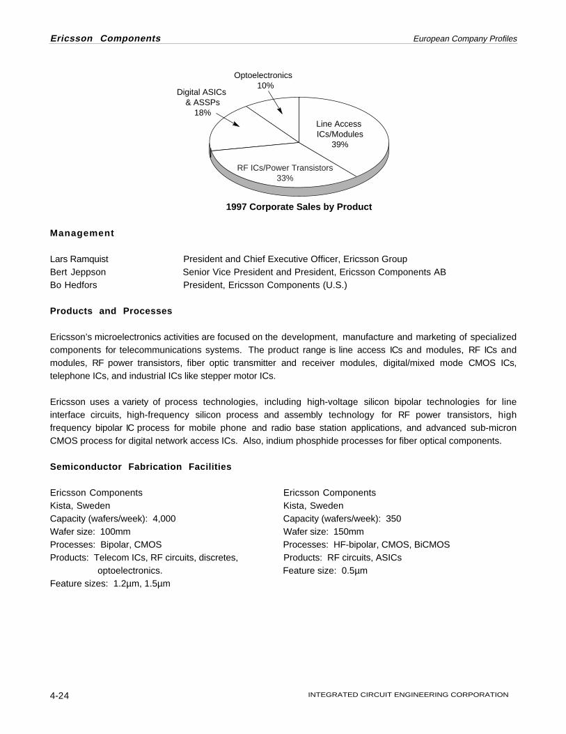
Optoelectronics 10%
1997 Corporate Sales by Product
Line Access ICs/Modules
39%
Digital ASICs & ASSPs
18%
RF ICs/Power Transistors33%
Management
Lars Ramquist President and Chief Executive Officer, Ericsson GroupBert Jeppson Senior Vice President and President, Ericsson Components ABBo Hedfors President, Ericsson Components (U.S.)
Products and Processes
Ericsson’s microelectronics activities are focused on the development, manufacture and marketing of specializedcomponents for telecommunications systems. The product range is line access ICs and modules, RF ICs andmodules, RF power transistors, fiber optic transmitter and receiver modules, digital/mixed mode CMOS ICs,telephone ICs, and industrial ICs like stepper motor ICs.
Ericsson uses a variety of process technologies, including high-voltage silicon bipolar technologies for lineinterface circuits, high-frequency silicon process and assembly technology for RF power transistors, highfrequency bipolar IC process for mobile phone and radio base station applications, and advanced sub-micronCMOS process for digital network access ICs. Also, indium phosphide processes for fiber optical components.
Semiconductor Fabrication Facilities
Ericsson Components Ericsson ComponentsKista, Sweden Kista, SwedenCapacity (wafers/week): 4,000 Capacity (wafers/week): 350Wafer size: 100mm Wafer size: 150mmProcesses: Bipolar, CMOS Processes: HF-bipolar, CMOS, BiCMOSProducts: Telecom ICs, RF circuits, discretes, Products: RF circuits, ASICs
optoelectronics. Feature size: 0.5µmFeature sizes: 1.2µm, 1.5µm

INTEGRATED CIRCUIT ENGINEERING CORPORATION 4-25
European Company Profiles Ericsson Components
Key Agreements
• Ericsson has maintained a strategic partnership with Texas Instruments since 1987. The partners extendedtheir alliance in 1992 when they announced plans to construct Ericsson's pilot production fab in Kista, Sweden.Under the agreement, TI installed its 0.5µm process technology in the plant in exchange for a greater share ofEricsson's semiconductor business. TI’s 0.35µm technology will be installed in the future. The agreement alsoincludes the cross-licensing of certain technologies and joint development of advanced ICs fortelecommunications applications.

4-26
INTEGRATED CIRCUIT ENGINEERING CORPORATION
GEC-Marconi Materials Technology Limited European Company Profiles
GEC-MARCONI MATERIAL S TECHNOLOGY LIMITED
GEC-Marconi Materials Technology LimitedCaswell, Towcester
Northamptonshire, NN128EQUnited Kingdom
Telephone: 1327-356428 or 1327-350581Fax: 1327-356775
Web Site: www.gmmt.co.uk
IC Manufacturer
GEC-Marconi Materials Technology Limited (GMMT), commonly referred to as the Caswell site, is one of tworesearch sites within GEC-Marconi Ltd.; GEC-Marconi Research Centre being the other site. GEC-Marconi Ltd.itself is a “business area” within General Electric Company, p.l.c.’s Electronic Systems and Defense Group, one ofthe fiscal 1997 consolidation’s five resulting groups.
Financial History
Sales from GEC-Marconi represented 32 percent of fiscal 1997 (6/30/97) total company sales of 11.147 billionPounds Sterling. Defense and Aerospace, Marconi’s primary businesses, is one of three areas GEC, p.l.c. hasdecided to focus upon for future growth. As a side note, GEC Plessey Semiconductor, divested in February1998, was not part of the Electronic Systems and Defense Group. Group R&D expenditures for fiscal 1996 were432 Pounds Sterling (up from 412 million in 1995), or 38.2 percent of total GEC R&D expenditures. However, asnoted below under Products and Processes, GMMT was collaborating with GEC Plessey Semiconductor (nowMitel Semiconductor) on wireless LAN product development. The status of the GMMT-Mitel effort isundetermined at press time.
GEC-Marconi Materials Technology Limited sales are as follows ($M):
1 9 9 6 1 9 9 7
Sales 10 12
Company Overview and Strategy
GEC-Marconi Materials Technology Limited (GMMT) conducts research and development, as well as produces,electronic, optoelectronic and pyroelectric devices and subsystems, and radar absorbent and transparentmaterials. Products are used primarily in military and aerospace (satellite, avionics) applications, though wirelessproducts for various commercial markets are in volume production and appear to be well-positioned. Whether thisproduct portfolio will remain part of GEC-Marconi, versus also being sold to Mitel or perhaps being transferred toGEC’s Telecommunications Group (e.g., GPT), is a rationalization matter GEC will likely have to deal with later in1998. (GMMT’s sister research site, GMRC, already supports product development for GPT in the AsynchronousTransfer Mode communications product arena).

INTEGRATED CIRCUIT ENGINEERING CORPORATION 4-27
European Company Profiles GEC-Marconi Materials Technology Limited
Organizationally, GMMT is composed of three Divisions: Microwave & Solid State, Materials, and Optoelectronics &Modules. The Materials Division is involved in research and development of Radar Absorbing Materials (RAMs)and Radar Transparent Materials, and so will not be profiled in this directory. Products and Processes availablefrom the other two Divisions are discussed below.
In addition to a direct sales organization for the UK and ROW, GMMT relies upon Daico Industries, Inc. for U.S.distribution and nine other distributors worldwide.
Management
Mike Geen Manager , GaAs Component Product LineStuart Cornelius Manager , Sales
Products and Processes
The Caswell site of GMMT conducts advanced development and production of GaAs semiconductors,optoelectronic devices (such as laser diodes) and sensor devices, including cooled infrared optical imagedetectors.
Among advanced technologies developed by GMMT is a micromachined, silicon-packaged optoelectronictransmit/receive terminal only 3mm thick for optical interconnections.
GMMT sees high performance radio networks as an important alternative technology to cable or fibre, especiallywhere mobility is required. Hence, GMMT's Caswell laboratory collaborated with GEC Plessey Semiconductors(sold to Mitel in February 1998) to develop wireless LANs (Local Area Networks) using GaAs monolithic microwaveintegrated circuits operating at 5.2GHz and achieving 23.5Mbits/sec data transmission. This “HIPERLAN” systemis emerging as a new European standard.
GMMT's latest wireless LAN is developed from a 2.4GHz transceiver now in volume production in the Caswell GaAsfoundry. Applications include point-of-sale terminals and cordless bar-code readers. GMMT’s advanced applications of GaAs technology include thousands of components for a phased arraysynthetic aperture radar for the European resource monitoring satellite. Additionally, to meet the increasinglydemanding needs of military radar and communication systems, a new GaAs production process commencedvolume production in fiscal 1997, of devices operating in the 35 to 40GHz range.
Improving over conventional techniques used to generate high voltage at low current, Caswell laboratories hasalso developed miniaturized voltage transformers based on piezoelectric ceramic, with devices only 4mm x 2mm x0.5mm generating 110 volts from a 3 volt source.
GMMT's Microwave & Solid State Division provides a complete Foundry Service and comprehensive DesignServices, as well as supplying ASICs and a wide range of standard products including MMIC amplifiers, small signaland power FETs, switches and LAN transceivers.

4-28
INTEGRATED CIRCUIT ENGINEERING CORPORATION
GEC-Marconi Materials Technology Limited European Company Profiles
GMMT has over 30 years of GaAs technology experience available to its GaAs Foundry services customers. Thecommercial GaAs Foundry itself was launched in 1985. It places great emphasis on process control andmanufacturability to ensure high yielding, reliable and reproducible processes. Currently, GMMT’s FoundryService provides a MMIC process with two basic options:
• F20 employs 0.5µm gate length MESFETs with standard depletion mode, recessed gate transistors andthrough substrate vias for use to 20GHz. F20 offers both switch/medium power and standard gain implants.
• H40 employs 0.25µm gate length low noise Pseudomorphic HEMT technology with mushroom gatetechniques for use to frequencies in excess of 40GHz.
The Microwave & Solid State Division is also developing new processes to further enhance existing technologiesand to offer designers the latest MMIC technology. These include:
• H100 0.10µm Pseudomorphic HEMT for applications up to 100GHz;• H40P Power HEMT process;• B20 HBT High speed digital/small signal analogue process; and• B20P HBT High power analogue process.
The Microwave & Solid State Division’s consultancy and design service range from initial feasibility studies to fullmultifunction MMIC and Module Design, reverse engineering, fabrication and test. Capabilities include design ofamplifiers, oscillators, mixers, phase shifters, attenuators and prescaler circuits for both microwave and millimeter-wave applications.
Microwave & Solid State Division’s Standard Products includes a selection of 11 standard switches, amplifiers andattenuators. Both general purpose devices operating up to 6GHz and wide-band devices operating up to 42GHzare available.
Based upon what it claims as highly integrated IP building blocks, the Microwave & Solid State Division hasdeveloped a range of ASIC wireless components including transceivers, power amplifiers and switches suited to anumber of wireless communications systems from 1.7 to 3GHz. These include DECT, DCS1800 and WirelessLocal Loop GaAs MMICs designed for emerging high data rate communications systems such as HIPERLAN,LMDS/LMCS and MVDS. Although RF ICs for wireless applications are the current focus, the Division has alsodeveloped a CP-packaged VCO for SART Applications which operates at 9.2 to 9.5GHz, 26dBm.

INTEGRATED CIRCUIT ENGINEERING CORPORATION 4-29
European Company Profiles GEC-Marconi Materials Technology Limited
GMMT’s Optoelectronics & Modules Division, formed 26 years ago, made major investments in its infrastructurebeginning in 1989. An ISO9001 accredited manufacturing facility with a substantial list of products in opto-electronics and GaAs microwave components was the result. The Division’s particular expertise includes
• DFB multi-quantum well lasers at 1300nm and 1500nm;• GaAs Mach-Zehnder Optical Modulators (DC - 50GHz);• High Speed InP pin diodes;• Broad Band LEDs;• Fibre Gratings;• Micro packaging;• Tunable DBR lasers; and• Microwave Fibre Optic Transmitters and Receivers.

4-30
INTEGRATED CIRCUIT ENGINEERING CORPORATION
Hyperstone Electronics GmbH European Company Profiles
HYPERSTONE ELECTRONICS GMBH
Hyperstone Electronics GmbHAm Seerhein 8
D-78467 KonstanzGermany
Telephone: 49 (7531) 98030Fax: 49 (7531) 51725
Web Site: www.hyperstone.com
Fabless IC Supplier
Regional Offices/Representative Regions
U.S.: Hyperstone Electronics USA, Inc. • Cupertino, CaliforniaTelephone: (408) 257-1057 • Fax: (408) 257-0713
Company Overview and Strategy
Hyperstone Electronics specializes in microprocessors that integrate DSP-instructions into the Hyperstone RISCarchitecture. This new class of microprocessor can be applied in a variety of areas such as telecommunications,office automation products, automotive applications, in personal digital assistants, multimedia, and all kinds of PC-boards and PCMCIA-cards. Hyperstone products are sold via local distributors in the U.S., throughout Asia, theU.K. and Italy.
Product s and Processes
The Hyperstone architecture is unique because dedicated DSP-instructions are fully integrated into theHyperstone RISC architecture and no separate DSP is required.
The Hyperstone E1-32 / E-16 Microprocessors combine the technology of a RISC Processor with an additionalDSP instruction set and on-chip microcontroller functions. This offers a powerful set of variable lengthinstructions. Programs for the Hyperstone require less than half the memory size of most RISC µPs and mostinstructions execute within one clock cycle. The fast multiply unit at high clock frequency makes it one of thefastest CPUs on the market with regard to DSP functionality. The following are some specifications of theseprocessors.
• Wide clock frequency range: 0.66MHz at 5V, 0.50MHz at 3.3V;• Operating voltage from 3.3V to 5V;• High performance: up to 30 MIPS with DRAMs, up to 66 MIPS with SRAMs;• Most instructions execute within one clock cycle;• Execution time for 1K Complex Fast Fourier Transform: 870 microseconds;• Low power consumption: typ. 240mW at 50MHz (3.3V);• Automatic power-down management;

INTEGRATED CIRCUIT ENGINEERING CORPORATION 4-31
European Company Profiles Hyperstone Electronics GmbH
• Address space: four memory areas of 1GB each;• Low system cost and easy board design through integrated control logic;• Built-in programmable bus controller;• Memory or I/O can be connected directly to CPU without any additional logic;• Bus widths: 8-, 16- or 32-bits, independent for each of the four memory areas;• Built-in programmable DRAM controller including refresh logic and parity;• Built-in timer;• Powerful instructions with variable length of 16-, 32- and 48-bits;• Compact program code requires just half the memory size of conventional RISCs;• Separate address- and data-bus;• On-chip RAM of 4Kbytes;• Fast pipelined DSP-multiply: 16- x 16-bit: 1cycle, 32- x 32-bit: 4 cycles; and• Multiply-accumulate within 1 cycle (pipelined).
Hyperstone also offers a complete set of development tools that consist of both software and hardware. Majorcomponents include the following.
• Programming Tools: C compiler, macro-assembler, linker with EPROM formatter and a library manager . • Debugging Tools: Source-level debugger with profiler.• Libraries: Full ANSI C run-time library and hyDSP DSP library .• Operating system: Multitasking Real-time operating system . • Hardware: PC-based development boards are available.

4-32
INTEGRATED CIRCUIT ENGINEERING CORPORATION
Matra MHS European Company Profiles
MATRA MHS
Matra MHS S.A.3, Avenue du Centre, BP 309
78054 St-Quentin-en-Yvelines CedexFrance
Telephone: (33) (1) 30-60-70-00Fax: (33) (1) 30-60-71-11
IC ManufacturerFounded: 1979
Regional Offices/Representative Locations
North America: TEMIC/Matra MHS, Inc. • Santa Clara, CaliforniaTelephone: (408) 970-3976 • Fax: (408) 988-3512
Financial History ($M)
1 9 9 2 1 9 9 3 1 9 9 4 1 9 9 5 1 9 9 6 1 9 9 7
Sales 110 125 130 150 145 300
Employees 850 900 915 925 925 925
Company Overview and Strategy
Matra MHS designs and manufactures advanced digital CMOS and BiCMOS circuits for such industries astelecommunications, aerospace and defense, automotive, and computer peripherals. The company’s main focusis on embedded controllers based on Intel-licensed 8-bit 80C51 and 80C251 microcontrollers. MHS’ activitiesalso include ASICs and ASSPs, CPLD/FPGA replacement, and specialty SRAMs.
Originally, Matra MHS was a member of TEMIC Semiconductors of the Integrated Circuits Division, which was themicroelectronic branch of the Daimler-Benz Group. TEMIC Semiconductors was formed in July 1992, by Daimler-Benz combining the products, experience, and technologies of its many semiconductor businesses into oneoperation.
In December 1997, TEMIC Semiconductors, which includes Integrated Circuits and Discrete Active ComponentsDivisions, was acquired by Vishay Intertechnology for $500 million. Then in March 1998, Vishay sold theIntegrated Circuits Division of TEMIC Semiconductors (Matra) to Atmel Corporation for $140 million.
Management
Michael Desbard Chief Executive Officer

INTEGRATED CIRCUIT ENGINEERING CORPORATION 4-33
European Company Profiles Matra MHS
Products and Processes
Matra MHS manufactures low-power, fast SRAMs (64K to 1M); specialty memories, including dual-port RAMs,FIFOs, and radiation-tolerant memories; SPARClet™ 32-bit RISC microprocessors for embedded control; 4-bit and8-bit MCUs; DSPs; ASICs; and ASSPs for data communication networks, automotive systems, and military andaerospace applications (dual-use concept).
Also, under a license agreement signed between TEMIC and Analog Devices in early 1997, Matra manufacturesradiation-tolerant 32-bit floating-point DSPs for radiation-sensitive applications. The DSP is based on AnalogDevices’ high-performance ADSP-21020 architecture and is built using a 0.6µm rad-hard CMOS process.
Matra MHS uses advanced CMOS and BiCMOS technologies in the manufacture of its ICs, including a 0.6µm,three-layer-metal CMOS process and a 0.5µm CMOS process. A 0.35µm process is being developed.
Semiconductor Fabrication Facilities
Matra MHSLa Chanterie-Route de GachetCP 300844087 Nantes Cedex 03FranceTelephone: (33) (2) 40-18-18-18Cleanroom size: 30,000 square feet (Class 1)Capacity (wafers/week): 3,500Wafer sizes: 125mm, 150mmProcesses: CMOS, BiCMOS, radiation-tolerant CMOSProducts: ASICs, ASSPs, MCUs, MPUs, SRAMs, DSPsFeature sizes: 0.5µm, 0.6µm, 0.8µm, 0.85µm (0.35µm in development)
Key Agreements
• In December 1998, TEMIC Semiconductors, which includes Integrated Circuits and Discrete ActiveComponents Divisions, was acquired by Vishay Intertechnology for $500 million. Then in March 1998, Vishaysold the Integrated Circuits Division of TEMIC Semiconductors, Matra, to Atmel Corporation for $140 million.
• Matra MHS has held a license for Intel’s 80C51 MCU family since 1981. The license has been continuedthrough the 80C251 family.
• Level One Communications and Matra MHS have a second-source agreement for on-line driver circuits.
• Matra MHS is a second source for Cypress Semiconductor’s fast 16K, 64K, and 256K asynchronous SRAMs.
• Matra MHS holds a license from Sun Microsystems for the production of SPARC-based products.
• In May 1995, DSP Group licensed to Matra MHS the rights to use its Pine and Oak DSP cores.

4-34
INTEGRATED CIRCUIT ENGINEERING CORPORATION
Melexis European Company Profiles
MELEXIS
MelexisRozendaalstraat 12
B – 8900 JeeperBelgium
Telephone: (32) (57) 226131Fax: (32) (57) 218089
IC Manufacturer
Regional Offices/Representative Locations
Europe: Melexis Research & Development Center - Tessenderlo, BelgiumTelephone: (32) (13) 670780 Fax: (32) (13) 672134
Melexis UK Ltd. – Chasetown Staffs, United KingdomTelephone: (44) 15 43 67 03 91 Fax: (44) 802 74 98 93
Melexis Germany/XFAB • Erfurt, GermanyTelephone: (49) 361 4205310 Fax: (49) 361 4205311
Melexis France • Paris, FranceTelephone: (33) 1 47 78 11 34 Fax: (33) 1 47 78 06 35
North America: Melexis USA • Sunnyvale, CaliforniaTelephone: (408) 749-1166 Fax: (408) 749-1718
Company Overview and Strategy
Melexis predominantly designs and produces ICs for automotive applications. This company with sales over $22million also produces ASICs, and supplies ICs to OEM customers.
Products and Processes
Melexis services include product development, program development, testing, fabrication, and packaging. Theyalso design and produce Integrated Systems, which comprise of logic and analog circuitry, power devices,memories, micro-controller cores and power supply regulators. Melexis uses a mixed mode test system, sincetheir devices have analog and digital parts.

INTEGRATED CIRCUIT ENGINEERING CORPORATION 4-35
European Company Profiles Melexis
Products are categorized as follows:
AnalogInterfaceConsumer/Automotive MOS MicrocomponentMPR
ASICsMixed Signal Automotive ASICs
Semiconductor Fabrication Facilities
Melexis Germany/XFABHaarbergstraBe 61D-99097 ErfurtDeutschlandTelephone: (49) 361 4205310Fax: (49) 361 4205311

4-36
INTEGRATED CIRCUIT ENGINEERING CORPORATION
Memory Corporation European Company Profiles
MEMORY CORPORATION
Memory CorporationThe Computer House
Dalkeith PalaceDalkeith, Edinburgh EH22 2NA
United KingdomTelephone: (44) 131-654-2576
Fax: (44) 131-654-0835Web Site: www.memcorp.com
Fabless IC SupplierFounded: 1993
Regional Offices/Representative Locations
U.S.: Memory Corporation, Inc. • Sunnyvale, CaliforniaTelephone: (408) 524-8741 • Fax: (408) 524-8749
Financial History ($), Fiscal Year Ends December 31
1 9 9 6 1 9 9 7
Sales 989 3,700Net Income (2,624) (1,600)
Employees — 40
Company Overview and Strategy
Memory Corporation licenses and sells design ASIC controllers used in the manufacture of DRAM modules andFLASH memory cards. The Company had focused its first efforts on applying its technology to the DRAM market.The first commercial application of Memory’s technology, called Variance Controlled Memory (VCM), has been inthe production of 16Mb memory modules with follow-on technology available or planned to support 64Mb andtheir variants such as EDO and SDRAM. Current DRAM support technologies include the following.
• a custom ASIC, encompassing the Partial Memory Engine;• memory test hardware optimized for defect capture; and• the software for testing and control of the production process and the test procedures.
Memory Corporation continues to develop new flash products, with the primary focus on software and a controllerASIC for use in the emerging file storage applications such as digital cameras and window CE computers, and aproduct introduction is scheduled for mid-1998.

INTEGRATED CIRCUIT ENGINEERING CORPORATION 4-37
European Company Profiles Memory Corporation
Memory’s technologies are well protected through a total of 20 patent applications to date, which together withcopyright over the Company’s proprietary software, provide powerful and wide-ranging intellectual protection overboth the Company’s products and its production processes.
Memory’s potential customer base are the world’s leading semiconductor and memory module manufacturers,such as Texas Instruments, Hitachi, Toshiba, and IBM.
Management
David Savage Chief Executive OfficerBill Hipp ChairmanAlan Sinclair Chief Technical OfficerMark Doughty Finance DirectorArun Kamat Vice President, Marketing
Products and Processes
Memory’s primary products include their VCM technology, and ASIC controllers – Advanced Partial MemoryEngine, MicroLock, and Flash Memory Controllers. Variance Controlled Memory (VCM) is a process allowingDRAMs with randomly distributed non-functioning cells to be utilized in full-function memory modules. The firststage of this VCM process is the testing of DRAMs to find the locations of the non-functioning cells. The secondstage is programming out the defective cells and replacing them with “good” cells from the substitute DRAM, all ofwhich involves intensive use of proprietary software, custom designed test equipment and redundancy controllerASIC.
Advanced Partial Memory Engine (APMEV4) is an ASIC controller used in a standard 72-pin SIMM, partiallydefective DRAM chips. The ASIC routes data to/from defective memory locations to alternative storage locations.The Controller uses 32-bits of main data memory and can also use 4-bits of replacement memory to implement afully functional SIMM. The number and type of DRAMs used to build the SIMM is flexible and the DRAMS used areselected to ensure that the total number of defects is within the mapping capabilities of the controller. Thecontroller also incorporates a built-in user programmable security feature and operates on a 3.3V power supply.
MicroLock is a custom electronic device fitted to memory modules, typically SIMMs. The device will disable theSIMM if it does not receive a security code within an allotted time. MicroLock is programmable and can beconfigured to operate in different applications.
Memory Corporation offers a range of DRAM SIMMs at 16 and 32Mb densities with parts manufactured based onVCM technology.
FlashSystem (FSM) is a proprietary controller architecture providing defect tolerance in Flash memories which isindependent of both the location and density of defects present in the memory components. It can support bothlinear and ATA Flash cards.

4-38
INTEGRATED CIRCUIT ENGINEERING CORPORATION
Memory Corporation European Company Profiles
Key Agreements
• In March 1998, Memory Corporation signed a license agreement with MicroLogic. Memory’s patented WideWord Defect Management technology will be incorporated into MicroLogic’s DRAM based solid state diskdrives. Memory will receive an unspecified royalty for every megabyte of memory shipped by MicroLogic.
• In February 1998, Memory Corporation and Datrontech Group formed a joint venture company, Dtec MemoryCorporation Limited (DMC). The new venture will be owned 51 percent by Memory and 49 percent byDatrontech. Dtech Memory Corporation will focus on the delivery of memory products and differentiatedcomputer memory solutions in the UK and Europe, using Memory’s technology in the latter.
• In late October 1997, Memory Corporation signed its first licensing agreement for MicroLock™ with Hsin-LinComputer. Memory sold and shipped to Hsin-Lin U.S. $500,000 of its chips, and Hsin Lin will pay a U.S.license fee for Microlock™ technology. Hsin-Lin will manufacture and sell Microlock™ application ASICs basedon Microlock™ technology and Microkey™ software.
• In August 1997, Memory Corporation signed a letter of intent with Micron Quantum Devices that forms aframework for an agreement on technology exchange and cross licensing. This allows Memory to accessMicron’s Flash Memory controller designs and for Micron to be granted the right to integrate Memory’sFlashSystem Manager™. The Letter-of-Intent grants Memory the rights to sell Micron Quantum Devices’controllers and is able to modify the controller design to target specific end-use applications. The agreementallows Memory and Micron to sell card manufacturers a FLASH memory controller for use with FLASH memorychips in an industry standard, such as PC card or Compact Flash Card for digital cameras.
• In July 1997, Memory Corporation signed a memorandum of understanding with Hsin Lin Computer Co. Ltd. ofTaiwan. This agreement allows both companies to jointly design and develop new memory products, whichthey will then jointly own and market. This alliance will focus on extending Memory’s partial memorytechnologies, including manufacturing process development, and in the next generation of memory securitydevices. The companies will also assist in the distribution of each other’s products in their geographical region.

INTEGRATED CIRCUIT ENGINEERING CORPORATION 4-39
European Company Profiles Micro Circuit Engineering
MICRO CIRCUIT ENGINEERING
Micro Circuit EngineeringAlexandra Way, Ashchurch Business Centre
Tewkesbury, Gloucestershire, GL20 8TBUnited Kingdom
Telephone: (44) (0) (1684) 297777Fax: (44) (0) (1684) 299435
Web Site: www.mce-asic.co.uk
IC ManufacturerFounded: 1981
Employees: 35
Company Overview and Strategy
Micro Circuit Engineering (MCE) designs and manufactures custom and standard products for a variety ofapplications and industry segments. MCE evolved from a group within Smiths Industries Aerospace in the late1960s and started trading under its own name in 1981. In 1997, total sales for MCE were $4.6 million.
With more than 500 years of semiconductor industry experience, MCE offers a full design and production servicefor custom ICs and remains a wholly-owned subsidiary of Smiths Industries Aerospace. Although an importantstrategic supplier to Smiths Industries, more than 75 percent of MCE’s sales are generated from outside thegroup, of which 20 percent is exported to USA, Western Europe and Japan.
MCE offers a wide range of CMOS and bipolar processes. Linear functions are available in CMOS, bipolar andBiCMOS technologies. The company provides gate arrays, mixed-signal arrays, digital and mixed-signal standardcells in technologies ranging from 5 micron to 0.5 micron. In addition to manufacturing ASICs, MCE alsomanufactures and supplies a range of standard products for MIL-STD-1553, MIL-STD-1760, Stanag 3910, ARINC429 and ARINC 629 data bus systems. Recently, MCE has introduced designing and manufacturing of MCMs(Multi-Chip Modules).
Management
John Shepherd General ManagerJohn Rayns Finance ManagerIan White Engineering ManagerColin Wadsworth Production ManagerMike Wopshott Quality ManagerStuart Gruszka Commercial & Marketing Manager

4-40
INTEGRATED CIRCUIT ENGINEERING CORPORATION
Micro Circuit Engineering European Company Profiles
Products and Processes
MOS MEMORY ANALOG
DRAM Amplifier
SRAM Interface
Flash Memory ✔ Consumer/Automotive
✔ EPROM Voltage Regulator/Reference
ROM Data Conversion
EEPROM Comparator
Other (Including Non-Volatile RAM) ✔ Other (Includes Telecom)
MOS LOGIC DIGITAL BIPOLAR
General Purpose Logic Bipolar Memory
✔ Gate Array General Purpose Logic
✔ Standard Cell ✔ Gate Array/Standard Cell
Field Programmable Logic Field Programmable Logic
✔ Other Special Purpose Logic Other Special Purpose Logic
MPU/MCU/MPR
MOS MICROCOMPONENT
MPU OTHER
MCU ✔ Full Custom IC
MPR Discrete
DSP Optoelectronic
Standard Products
MCE offers a range of components and modules for MIL-STD-1553, MIL-STD -1760, Stanag 3910, ARINC 429and ARINC 629 data bus standards.
MCMs
MCE provides designing and manufacturing capability for both passive and active silicon substrate MCMs.
ASICs
MCE offers digital gate arrays from 300 to 80K gates in a range of CMOS from 5 to 0.8 micron and mixed-signalarrays in 3 micron CMOS. Standard cell and full custom ASICs can mix analog, memory and fuses withconventional digital circuitry, and can be fabricated down to 0.5 micron.
Semiconductor Fabrication Facilities
In addition to MCE’s manufacturing capabilities, MCE has access to a number of world class silicon foundries inNorth America and Western Europe.
The company uses sub-contract assembly houses in the Pacific Rim and in Europe. MCE maintains a militaryqualified ceramic assembly and test facility at Tewkesbury, UK headquarters.

INTEGRATED CIRCUIT ENGINEERING CORPORATION 4-41
European Company Profiles Micronas
MICRONAS
Micronas SemiconductorWorld Trade Center
Leutschenbachstrasse 95CH-8050 Zurich, Switzerland
Telephone: (41) (1) 308-3923Fax: (41) (1) 308-3500
IC Manufacturer
Financial History ($M)
1 9 9 4 1 9 9 5 1 9 9 6 1 9 9 7 *
Sales 37 74 84 —Capital Expenditures 1 5 4 —
Employees 169 334 399 400
*Company did not disclose.
Company Overview and Strategy
Micronas specializes in the design, development, and production of high-precision analog and mixed-signal ICs,digital signal processors (DSPs), surface acoustic wave (SAW) filters, microsensors, Hall sensors and systems.With this interdisciplinary knowledge, the company develops both application-specific and custom-designedproducts for telecommunications, consumer and automotive electronics applications.
The multinational Micronas Group concentrates on market-driven solutions that offer cost savings andminiaturization of functions. Micronas maintains several wafer fabrication facilities in Europe, as well ascollaborating with a large foundry in Asia.
Management
Jürgen Kurb Chief Executive OfficerGery Oberrauter Manager, Telecom BusinessThomas Fischer Manager, Consumer Business

4-42
INTEGRATED CIRCUIT ENGINEERING CORPORATION
Micronas European Company Profiles
Products and Processes
Micronas provides a wide range of products, including mixed-signal ICs, multi-technology modules (MTMs), hybridsystems and SAW filters for telecommunications applications (e.g., cellular phones and base stations). Thecompany also supplies mixed-signal ASICs, DSPs, microcontrollers, high-accuracy pressure sensor systems,protection circuitry and Hall sensors for consumer and automotive applications.
Micronas uses a modular molybdenum gate bipolar-enhanced complementary metal oxide semiconductor(BeCMOS) technology, in conjunction with the ability to integrate thin-film resistors and capacitors, to meet theneeds of accurate and stable mixed-signal applications. This process supports nominal power supply voltagesbetween 1.2V and 40V for low power consumption.
A recently acquired division, Micronas Intermetall GmbH, produces DSPs, MPUs, MCUs, video and audioencoders/decoders, signal converters and Hall-effect sensors. These products are manufactured in a range ofCMOS process technologies with feature sizes of 1.0µm to 0.5µm. Technologies include advanced mixed-signalcapability and flash memories.
Semiconductor Fabrication Facilities
Micronas OyP.O. Box 51FIN-02771 Espoo, FinlandTelephone: (358) (9) 80521Cleanroom size: 4,300 square feetCapacity (wafers/week): approx. 2,000Wafer size: 100mmProcess: Moly-gate CMOSProducts: Mixed-signal and analog ICs, foundry services
Micronas Semiconductor SACh. Chapons-des-PresCH-2022 Bevaix, SwitzerlandTelephone: (41) (32) 847-0111Cleanroom size: 21,500 square feetCapacity (wafers/week): approx. 2,000Wafer size: 100mmProcesses: Bipolar, moly-gate CMOS, lift-off and dry etch processesProducts: Hybrids, SAW filters, pressure sensors, foundry services
Micronas Intermetall GmbHP.O. Box 840, D-79008 Freiburg, GermanyTelephone: (49) 761-5170Cleanroom size: 33,000 square feetCapacity (wafers/week): 4,000Wafer size: 150mmProcess: CMOSProducts: ICs, digital signal processors, microcontrollers, Hall sensors

INTEGRATED CIRCUIT ENGINEERING CORPORATION 4-43
European Company Profiles Micronas
Key Agreements
• In April 1998, Genesis and Micronas Intermetall announced they are using each other’s chips to produce aunique set of video processing reference designs.

4-44
INTEGRATED CIRCUIT ENGINEERING CORPORATION
Newport Wafer-Fab European Company Profiles
NEWPORT WAFER-FAB (NWL)
Newport Wafer-Fab LimitedCardiff Road
Duffryn, NewportNP9 1YJ, South Wales
United KingdomTelephone: (44) (1633) 810121
Fax: (44) (1633) 810820Email: [email protected] Site: www.newportwaferfab.com
IC Manufacturer
Employees: 575
Regional Headquarters/Representative Locations
North America: Newport Wafer Fab Ltd. • San Jose, CaliforniaTelephone: (408) 436-3053 • Fax: (408) 436-0246
Company Overview and Strategy
NWL (Newport Wafer-Fab Limited) is Europe’s leading dedicated silicon wafer foundry. As a “pure-play” foundry,NWL focuses on providing leading-edge digital and mixed-signal technology, customer specific processesincluding BiCMOS, high voltage and a variety of digital imaging applications.
NWL operates three manufacturing facilities offering 6- and 8-inch wafers at their headquarters in Wales, UnitedKingdom. NWL process offerings include 1.5 micron to 0.5 micron capabilities. Their newest facility, Fab 3provides customers access to 0.35 micron technology. In 1999, the company will offer customers 0.25 microntechnology production.
Established in 1992, NWL is a subsidiary of Hong Kong based QPL International Holdings Limited and a sistercompany of ASAT which offers assembly and test capabilities. Located near ASAT UK, the organization offerstotal turnkey services to the semiconductor industry.
Management
Steve Byars Chief Executive OfficerJohn Elder Director, OperationsGareth Jones Director, Sales and MarketingSteve Della Rocchetta Executive Vice President, COO U.S. Branch
INTEGRATED CIRCUIT ENGINEERING CORPORATION 4-45
European Company Profiles Newport Wafer-Fab
Products and Processes
NWL’s foundry services consist of two dedicated fabs with double- and triple-level metal, single- and double-levelpoly CMOS wafer fabrication down to 0.5µm feature sizes. With the completion of Fab 3, which is just coming on-line this year (1998), the company will offer 200mm wafer capacity in 0.5µm CMOS, moving to 0.35µm.
Semiconductor Fabrication Facilities
During 1996, NWL completed the conversion from 100mm to 150mm wafer production at its Fab 1 facility. Alsoduring 1996, NWL completed construction of Fab 2 and began construction on Fab 3. Fab 3 is a $350 million200mm wafer fab.
Newport Wafer-Fab LimitedCardiff RoadDuffryn NewportNP9 1YJ South WalesUnited Kingdom
FAB 1
Capacity (wafers/week): 5,000Wafer size: 6 inchesProcess: Digital CMOS, Mixed-signal CMOS, HV CMOS, BiCMOS, LCDProducts: NoneFeature sizes: 0.7µm - 1.5µm
FAB 2
Capacity (wafers/week): 1,250Wafer size: 6 inchesProcess: Digital CMOS, Mixed-signal CMOS, HV CMOS, BiCMOS, Digital ImagingProducts: NoneFeature sizes: 0.35µm - 0.7µm
FAB 3
Capacity (wafers/week): 3,750Wafer size: 8 inchesProcess: Digital CMOS, Mixed-signal CMOS, BiCMOSProducts: NoneFeature sizes: 0.25µm - 0.5µm
4-46
INTEGRATED CIRCUIT ENGINEERING CORPORATION
Newport Wafer-Fab European Company Profiles
Key Agreements
• March 1998, Newport Wafer-Fab Limited has licensed SGS-Thomson Microelectronics’ process technologyfor the production of 0.35 micron and 0.25 micron digital logic and mixed-signal devices.
The process technology will initially be transferred to NWL’s Fab 3 in Wales, U.K.
• Newport Wafer-Fab Limited announced that it has selected Artisan Components Inc. to provide ProcessPerfect™ Standard Cell Libraries, I/O Libraries and embedded SRAM generators for NWL’s 0.5 micron and0.35 micron CMOS technologies.
In a multi-million pound deal between the two companies, NWL has received the distribution rights to theselibraries and generators.
• Catalyst signed on Newport Wafer-Fab Ltd. in May 1995 for the manufacture of its EEPROMs and for Processtechnology development.

INTEGRATED CIRCUIT ENGINEERING CORPORATION 4-47
European Company Profiles Oxford Semiconductor
OXFORD SEMICONDUCTOR
Oxford Semiconductor Limited68 Milton Park
Abingdon, Oxon OX144RXUnited Kingdom
Telephone: (44) 1235-861461Fax: (44) 1235-821141
Web Site: www.oxsemi.com
Fabless IC ManufacturerFounded: 1992
Regional Headquarters/Representative Locations
Europe: Alt Technologies Ltd. • Hampshire, United KingdomTelephone: (44) 1256-81640 • Fax: (44) 1256-811876
Company Overview and Strategy
Oxford Semiconductor is dedicated to the design and supply of ASICs. They offer comprehensive expertise inGate Array, Field Programmable Gate Array, Standard Cell and Full Custom solutions. ASICs can be designed fromthe customer's system specification, as a turnkey project, or can be handed-over as a previously completeddesign, to be fabricated by one of Oxford’s foundry partners. ALT Technologies operates as a salesrepresentative for Oxford Semiconductor. The Company’s ASICs and ASSPs combine reliability and highperformance with highly integrated functionality to provide low component count, and cost effective solutions.
Management
James Lewis Sales and Marketing DirectorJalil Oraee, Ph.D. Technical DirectorTim Cook, Ph.D. Managing DirectorNick Cross Finance Director
Products and Processes
Oxford Semiconductor offers complete flexibility in interfacing with customers. ASIC design services fall into fourcategories, as described below.
• Full-turnkey ASIC Design – the customer provides a complete specification. Oxford then carries out theentire development. VHDL synthesis techniques are used.
• Netlist Hand-over – The customer develops their ASIC in-house using schematic entry VHDL, Verilog, etc.,and then Oxford completes the ASIC development.

4-48
INTEGRATED CIRCUIT ENGINEERING CORPORATION
Oxford Semiconductor European Company Profiles
• FPGA Conversion – The customer develops and evaluates their design using FPGA or DPLDs. Oxfordthen re-targets the design into a suitable ASIC technology to enable the customer to take advantage ofbeneficial volume pricing.
• Silicon processing – The customer has completed as ASIC development and then Oxford carries out designrule check and fault grading before fabricating ASIC devices.
Examples of some of the Oxford ASIC designs are:
• Data communication ASICs - highly programmable asynchronous data communications engines, OctalUART, PC communication port chips;
• ASICs for PCs and peripherals – graphics tablet ICs, PC chipsets, data storage devices, software securitykey; and
• ASICs for Other Markets – control chips for industrial control, weapons systems actuator control, safetysystems, and global positioning systems.
Semiconductor Fabrication Facilities
Oxford Semiconductor has access to several silicon foundries located in the Far East, Europe and the U.S.Manufacturing processes use 0.6 micron and 0.8 micron CMOS technology for dual or triple layer metal designs.

INTEGRATED CIRCUIT ENGINEERING CORPORATION 4-49
European Company Profiles Philips Semiconductors
PHILIPS SEMICONDUCTORS
Philips Semiconductors BVBuilding BAE2 19
P.O. Box 2185600MD Eindhoven, The Netherlands
Telephone: (31) (40) 723-520Fax: (31) (40) 723-085
Web Site: www.semiconductors.philips.com
IC Manufacturer
Regional Headquarters/Representative Locations
North America: Philips Semiconductors • Sunnyvale, CaliforniaTelephone: (408) 991-2000 • Fax: (408) 991-2311
Japan: Philips Semiconductors • Minato-ku, Tokyo, JapanTelephone: (81) (3) 3740-5130 • Fax: (81) (3) 3740-5077
Asia-Pacific: Philips Taiwan Ltd. • Taipei, TaiwanTelephone: (886) (2) 382-4443 • Fax: (886) (2) 382-4444
Financial History, Fiscal Year Ends December 31
1 9 9 2 1 9 9 3 1 9 9 4 1 9 9 5 1 9 9 6 1 9 9 7
Corporate (NLG in millions)Sales NLG58,527 NLG58,825 NLG60,977 NLG64,462 NLG69,195 NLG76,453Net Income NLG(900) NLG1,965 NLG2,049 NLG2,684 NLG723 NLG3,291
Semiconductor Business ($M)Sales 2,055 2,250 2,866 3,994 4,196 4,451
IC Sales 1,480 1,640 2,106 2,936 3,253 3,447Discrete Sales 575 610 760 1,058 943 1,004
R&D Expenditures 450 555 505Capital Expenditures 140 134 320 750 720 385
Employees 20,000 19,000 21,000 26,000 26,000 27,000

4-50
INTEGRATED CIRCUIT ENGINEERING CORPORATION
Philips Semiconductors European Company Profiles
Company Overview and Strategy
Philips Semiconductors is a division of Philips Electronics NV, one of the world's largest electronics companies,with sales of about $44 billion (1997) and over 270,000 employees worldwide. Philips Electronics was founded in1891 to manufacture and market the newly invented electric light bulb. The company has expanded widely sincethen and today the breadth and diversity of its activities is clear from the names of its product divisions: Lighting,Sound, and Vision; Domestic Appliances and Personal Care; Communication Systems; Industrial Electronics;Medical Systems; and Components and Semiconductors.
ConsumerProducts
31%
Miscellaneous2%
1997 Corporate Sales by Business Sector
ProfessionalProducts/Systems
17%
Components/Semiconductors
20%
Lighting13%
Software/Services
17%
Philips began manufacturing electronic components in 1921 for in-house use. External component sales beganin the late 1940's and in 1964, the Components Division was formed. Philips Semiconductors was created out ofPhilips Components in 1991 as a separate product division to bring greater focus to Philips' integrated circuit anddiscrete semiconductor businesses. Today, Philips Semiconductors ranks among the world's largestsemiconductor producers, providing a wide range of commodity products (standard logic ICs, microcontrollers,and discretes) and advanced application-specific devices for the communications, multimedia, consumerelectronics, identification, and automotive markets.
Consumer45%
Military/Government1%
1997 Semiconductor Salesby End-Use Market
Industrial14%
EDP14%
Communication19%
Automotive7%
Europe42%
Japan4%
1997 Semiconductor Salesby Geographic Region
Asia-Pacific35%
Americas19%

INTEGRATED CIRCUIT ENGINEERING CORPORATION 4-51
European Company Profiles Philips Semiconductors
Philips Semiconductors is structured into four business groups: Consumer ICs, Communications and Multimedia,Auto/ID/Storage and Logic ICs, and Discrete Semiconductors. Approximately 15 percent of PhilipsSemiconductors’ devices are sold to other business sectors within Philips.
Building on its strategy to establish itself as a leader in the multimedia market, Philips Semiconductors acquired themultimedia IC business of Western Digital Corporation in November 1995. Under terms of the agreement, Philipsacquired all of the assets of Western Digital’s Multimedia Products Unit, which included the RocketCHIP family ofICs and the Paradise graphics accelerator cards (Philips shut down the card business in 1996). In addition, Philipsand German software vendor Spea Software AG forged an agreement aimed at jointly developing highperformance 3D multimedia ICs for PCs and game equipment.
Management
Arthur van der Poel Chairman and Chief Executive Officer, Philips SemiconductorsStuart McIntosh Chief Operations OfficerScott McGregor Senior Vice President and GM, Emerging Business UnitRoss Anderson Vice President and GM, Auto/ID/Storage and Logic IC Business GroupGuenther Dengel Vice President and GM, Consumer IC Business GroupLeon Husson Vice President and GM, Discrete Semiconductor Business GroupCees Jan Kooman Vice President and GM, Communications and Multimedia Business GroupWalter Conrads Vice President and GM, International Sales and Marketing
Products and Processes
Philips' semiconductor products are split up by business group below.
Consumer IC Group Auto/ID/Storage and Logic IC Group• digital audio circuits • automotive circuits• radio/TV/VCR signal processing ICs • data communications chips• motor drive/control circuits • RF/telecom ICs• data conversion devices • standard logic devices• monitor ICs • PLDs
Communications and Multimedia Group Discrete Semiconductors Group• microcontrollers • power MOSFETs• telecommunications devices • power transistors• digital video/audio circuits • amplifiers

4-52
INTEGRATED CIRCUIT ENGINEERING CORPORATION
Philips Semiconductors European Company Profiles
MOS MEMORY ANALOG
DRAM ✔ Amplifier
SRAM ✔ Interface
Flash Memory ✔ Consumer/Automotive
EPROM ✔ Voltage Regulator/Reference
ROM ✔ Data Conversion
EEPROM ✔ Comparator
Other (Including Non-Volatile RAM) ✔ Other (Includes Telecom)
MOS LOGIC DIGITAL BIPOLAR
✔ General Purpose Logic ✔ Bipolar Memory
Gate Array ✔ General Purpose Logic
Standard Cell Gate Array/Standard Cell
✔ Field Programmable Logic ✔ Field Programmable Logic
✔ Other Special Purpose Logic Other Special Purpose Logic
MPU/MCU/MPR
MOS MICROCOMPONENT
MPU OTHER
✔ MCU Full Custom IC
✔ MPR ✔ Discrete
✔ DSP Optoelectronic
Multimedia ICs
Philips sees multimedia as a key growth area. The company began marketing MPEG-1 and MPEG-2 audio/videocompression chips in 1995. Through its acquisition of Western Digital’s multimedia IC business, Philips now offersleading-edge 3D graphics coprocessors and full-motion video/graphics accelerators. For CD systems, Philipsprovides devices for high-speed CD-ROM drives and Video-CD and CD-Recordable/Erasable systems.
Philips also began selling its powerful programmable digital signal processor, named TriMedia, in late 1996. Thefirst generation single-chip TriMedia media processor has the power (up to four billion operations per second) toprocess audio, video, graphics, and communications data concurrently. Specifically designed for multimediaprocessing, the TriMedia processor uses a VLIW (very long instruction word) architecture and innovativescheduling compiler to process multiple operations in a single clock cycle. The TriMedia family of processors alsooffers an open development environment.
Audio and Video ICs
Philips offers over 200 ICs for television and video applications, such as wide-screen TVs, surround-soundfunctions, video cameras, VCRs, and monitors. The company also offers a wide range of digital-to-analog (D/A)and analog-to-digital (A/D) converters, power amplifiers, and DSPs for audio processing.
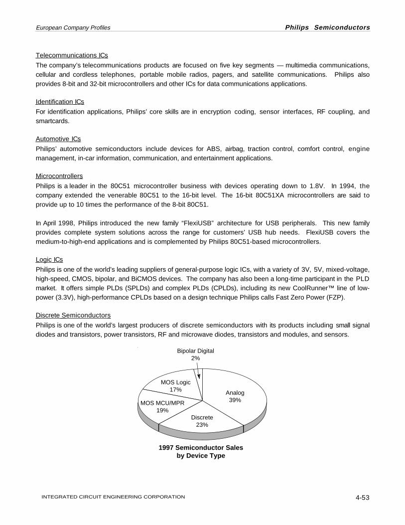
INTEGRATED CIRCUIT ENGINEERING CORPORATION 4-53
European Company Profiles Philips Semiconductors
Telecommunications ICs
The company’s telecommunications products are focused on five key segments — multimedia communications,cellular and cordless telephones, portable mobile radios, pagers, and satellite communications. Philips alsoprovides 8-bit and 32-bit microcontrollers and other ICs for data communications applications.
Identification ICs
For identification applications, Philips’ core skills are in encryption coding, sensor interfaces, RF coupling, andsmartcards.
Automotive ICs
Philips’ automotive semiconductors include devices for ABS, airbag, traction control, comfort control, enginemanagement, in-car information, communication, and entertainment applications.
Microcontrollers
Philips is a leader in the 80C51 microcontroller business with devices operating down to 1.8V. In 1994, thecompany extended the venerable 80C51 to the 16-bit level. The 16-bit 80C51XA microcontrollers are said toprovide up to 10 times the performance of the 8-bit 80C51.
In April 1998, Philips introduced the new family “FlexiUSB” architecture for USB peripherals. This new familyprovides complete system solutions across the range for customers’ USB hub needs. FlexiUSB covers themedium-to-high-end applications and is complemented by Philips 80C51-based microcontrollers.
Logic ICs
Philips is one of the world’s leading suppliers of general-purpose logic ICs, with a variety of 3V, 5V, mixed-voltage,high-speed, CMOS, bipolar, and BiCMOS devices. The company has also been a long-time participant in the PLDmarket. It offers simple PLDs (SPLDs) and complex PLDs (CPLDs), including its new CoolRunner™ line of low-power (3.3V), high-performance CPLDs based on a design technique Philips calls Fast Zero Power (FZP).
Discrete Semiconductors
Philips is one of the world’s largest producers of discrete semiconductors with its products including small signaldiodes and transistors, power transistors, RF and microwave diodes, transistors and modules, and sensors.
Analog39%
1997 Semiconductor Salesby Device Type
MOS MCU/MPR19%
MOS Logic17%
Discrete23%
Bipolar Digital2%

4-54
INTEGRATED CIRCUIT ENGINEERING CORPORATION
Philips Semiconductors European Company Profiles
The technologies used in the manufacture of Philips' semiconductors include advanced bipolar, CMOS, BiCMOS,and BCDMOS including submicron. Philips’ leading edge CMOS process technologies include its 0.5µm three-layer-metal C100 process and its 0.35µm C075 process, which is available with four or five layers of metal. Manynew, advanced product lines are based on the company's proprietary QUBiC BiCMOS process, which is currentlyat the 0.8µm geometry level.
Semiconductor Fabrication Facilities
Philips Semiconductors Philips SemiconductorsGerstweg 2 Gerstweg 2Building ANO 121 Building ANO 1216534 AE Nijmegen, The Netherlands 6534 AE Nijmegen, The NetherlandsMOS2 MOS3Telephone: (31) (80) 532-544 Telephone: (31) (80) 532-544Cleanroom size: 34,440 square feet (Class 10) Cleanroom size: 32,300 square feet (Class 10)Capacity (wafers/week): 10,250 Capacity (wafers/week): 5,000Wafer size: 100mm Wafer size: 150mmProcesses: CMOS, DMOS Processes: CMOS, BiCMOSProducts: Logic ICs Products: Logic and analog ICs, MCUsFeature sizes: 1.2µm, 2.0µm, 3.0µm Feature sizes: 0.6µm, 0.7µm, 0.8µm
Philips Semiconductors Philips SemiconductorsGerstweg 2 Gerstweg 2Building ANO 121 Building ANO 1216534 AE Nijmegen, The Netherlands 6534 AE Nijmegen, The NetherlandsTelephone: (31) (80) 532-544 Telephone: (31) (80) 532-544MOS4YOU (Yield Output Utilization) CIC/AN FabCleanroom size: 74,270 square feet (Class 0.1-1) Cleanroom size: 48,440 square feet (Class 10)Capacity (wafers/week): 4,600 Capacity (wafers/week): 7,500Wafer size: 200mm Wafer size: 125mmProcess: CMOS Processes: Bipolar, BiCMOSProducts: Consumer and communications ICs Products: Digital bipolar and analog ICsFeature sizes: 0.35µm, 0.5µm Feature sizes: 1.75µm, 3.0µm
Philips Semiconductors Philips SemiconductorsGerstweg 2 P.O. Box 10Building ANO 121 Electronicaweg 16534 AE Nijmegen, The Netherlands 9500AA Stadskanaal, The NetherlandsTelephone: (31) (80) 532-544 Telephone: (31) (599) 032330Cleanroom size: 32,300 square feet (Class 1,000) Cleanroom size: 26,900 square feet (Class 10,000)Capacity (wafers/week): 3,750 Capacity (wafers/week): 17,500Wafer size: 100mm Wafer size: 100mmProcesses: MOS, bipolar Process: BipolarProducts: Discretes Products: DiscretesFeature sizes: 0.7µm-100µm Feature sizes: 1.0µm, 3.0µm

INTEGRATED CIRCUIT ENGINEERING CORPORATION 4-55
European Company Profiles Philips Semiconductors
Philips Semiconductors Philips Semiconductors2, rue de la Girafe, BP 5120 Microelectronic Center14043 Caen Cedex, France 2, rue de la Girafe, BP 5120Telephone: (33) (2) 31-45-2114 14043 Caen Cedex, FranceFab 1 Telephone: (33) (2) 31-45-2114Cleanroom size: 37,675 square feet Fab 2Capacity (wafers/week): 6,250 Cleanroom size: 24,750 square feetWafer size: 125mm Capacity (wafers/week): 2,500Processes: Bipolar, BiMOS, MOS Wafer size: 150mmProducts: Discretes Process: BiCMOSFeature size: 1.2µm Products: Consumer, telecom, and logic ICs
Feature size: 0.8µm
Philips Semiconductors Philips SemiconductorsP.O. Box 54 02 40 P.O. Box 54 02 40Stresemannallee 101 Stresemannallee 10120043 Hamburg, Germany 20043 Hamburg, GermanyTelephone: (49) (40) 32960 Telephone: (49) (40) 32960CIC Fab I&A FabCleanroom size: 11,840 square feet (Class 100) Cleanroom size: 12,920 square feet (Class 10)Capacity (wafers/week): 3,125 Capacity (wafers/week): 4,500Wafer size: 125mm Wafer size: 125mmProcesses: CMOS, bipolar, BiCMOS Processes: CMOS, NMOS, BiCMOSProducts: MCUs Products: Consumer ICsFeature size: 1.5µm Feature sizes: 0.8µm-1.2µm
Philips Semiconductors Philips SemiconductorsP.O. Box 54 02 40 Bramhall More LaneStresemannallee 101 Hazel Grove, Stockport20043 Hamburg, Germany SK7 5BJ England, United KingdomTelephone: (49) (40) 32960 Telephone: (44) (61) 48 30 011Cleanroom size: 7,300 square feet (Class 1,000) Powerfab 1 and PowerMOSCapacity (wafers/week): 5,500 Cleanroom size: 45,210 square feet (Class 10-100)Wafer size: 100mm Capacity (wafers/week): 14,000Process: Bipolar Wafer size: 125mmProducts: Discretes Processes: MOS, bipolarFeature size: 2.5µm Products: Discretes
Feature sizes: 4.0µm-35µm

4-56
INTEGRATED CIRCUIT ENGINEERING CORPORATION
Philips Semiconductors European Company Profiles
Crolles Joint Research Center Philips SemiconductorsCrolles, France 811 East Arques AvenueCleanroom size: 21,340 square feet Sunnyvale, California 94088-3409Wafer size: 200mm Telephone: (408) 991-2000Processes: CMOS, BiCMOS Fab 1Products: R&D Cleanroom size: 32,300 square feet (Class 100)Feature sizes: 0.25µm-0.8µm Capacity (wafers/week): 5,750(R&D facility jointly operated by Philips, Wafer size: 100mmSGS-Thomson, and CNET). Process: Bipolar
Products: Linear ICsPhilips Semiconductors Feature sizes: 2.0µm-4.0µm9201 Pam American Expressway N.E.Albuquerque, New Mexico 87184 Philips SemiconductorsTelephone: (505) 822-7000 9201 Pan American Expressway N.E.Fab 22 Albuquerque, New Mexico 87184Cleanroom size: 32,300 square feet (Class 100) Telephone: (505) 822-7000Capacity (wafers/week): 8,250 Fab 23Wafer sizes: 100mm Cleanroom size: 43,050 square feet (Class 10)Processes: CMOS, bipolar Capacity (wafers/week): 4,175Products: MCUs Wafer size: 150mmFeature size: 1.0µm Processes: CMOS, BiCMOS
Products: MCUs, PLDs, ASICsFeature sizes: 0.65µm, 0.8µm (0.5µm in 1997)
SubMicron Semiconductor Technologies GmbH (SMST)Schoenaicherstrasse 220Boeblingen Hulb, GermanyCleanroom size: 107,640 square feet, Class 1Capacity (wafers/week): 4,000Wafer size: 200mmProcess: CMOSProducts: DRAMs, logic ICsFeature size: 0.65µm(Joint venture with IBM Microelectronics,see Key Agreements).
Philips also owns 34 percent of Taiwan Semiconductor Manufacturing Co. (TSMC) and 38 percent of AdvancedSemiconductor Manufacturing Corp. of Shanghai (ASMC). For data on the fab facilities of ASMC and TSMC, seethe profiles of each in this publication.
Philips has 11 assembly/test facilities located around the world. These are located in The Netherlands, England,Belgium, France, Germany, Thailand, China, Malaysia, Hong Kong, Korea, and the Philippines.
INTEGRATED CIRCUIT ENGINEERING CORPORATION 4-57
European Company Profiles Philips Semiconductors
Key Agreements
• In March 1998, Genesis Microchip and Philips Semiconductors announced that its Z1MP and Z1CMPreference designs for LCD applications will use Philips’ TDA 8752 triple high-speed analog-to-digital converter(ADC) chip.
• In February 1998, Philips Semiconductors and Hitachi Ltd. announced an agreement to cooperate in thedevelopment of contactless smartcard ICs utilizing Philips Semiconductors’ MIFARE® Technology. After an in-depth evaluation of available technologies, Hitachi has chosen to take a technology transfer contract fromPhilips Semiconductors.
• In November 1997, Philips Semiconductors’ Handheld Computing Group announced that Samsung hadchosen its TwoChipHCG* Plus processor for Samsung’s new Smartphone SCS-100 Infomobile, the firstWindows CE 2.0-based device which combines a mobile computer and a CDMA/AMPS cellular phone into asingle portable unit.
• In November 1997, Philips Semiconductors and NEC Corporation signed a partnership agreement targetingadvanced consumer applications with the MIPS® microprocessor architecture. In the initial stage of theagreement, NEC will provide its VR4300™ series 64-bit processor core, and Philips Semiconductors will workwith NEC on chip integration and support technologies to make MIPS® the global standard platform for theconsumer area.
• Philips licensed the ARM7 32-bit microprocessor core from Advanced RISC Machines in early 1997.
• In April 1996, Philips announced a wafer sourcing agreement with TriQuint Semiconductor. Under theagreement, GaAs ICs developed at Philips Microwave Limeil, France, will be produced by TriQuint and thenmarketed only by Philips.
• Philips revealed in 1995, a partnership with German software vendor Spea Software AG to jointly develop highperformance 3D multimedia ICs for PC and game equipment applications.
• In 1994, Philips agreed with IBM Microelectronics to form a joint venture to manufacture ICs at IBM's fab facility inBoeblingen Hulb, Germany. Philips holds 51 percent and IBM 49 percent of the new company, calledSubMicron Semiconductor Technologies GmbH (SMST). SMST is supplying products solely to IBM andPhilips, manufacturing DRAMs for IBM and logic ICs for Philips. Separately, Philips acquired the rights to IBM’s16M DRAM technology for embedded applications. Embedded DRAM products will also be produced bySMST.
• Philips formed a joint venture in China in 1994 with Northern Telecom and the Chinese government. The newcompany, called Advanced Semiconductor Manufacturing Corp. (ASMC), took over Philips' wafer fab in China.In 1996, the partners completed the installation of a new 150mm wafer line for processing 0.8µm BiCMOS and1.0µm CMOS circuits.
• Philips Semiconductors has a technology partnership with TI-subsidiary Silicon Systems concerning disk driveICs.

4-58
INTEGRATED CIRCUIT ENGINEERING CORPORATION
Philips Semiconductors European Company Profiles
• Philips, TI, and Hitachi formed a pact in 1993 covering joint development and alternate sourcing of FutureBusand BiCMOS logic IC products.
• Philips extended its patent cross-license agreement with Intel to include all of each other’s semiconductordevices except certain proprietary Intel MPUs and Philips’ video products. The agreement is now valid throughthe year 2000. In addition, the two companies established an agreement to develop a new family of 8-bitMCUs, based on an upgraded 80C51 core.
• Philips has a license from Silicon Graphics for 32-bit and 64-bit MIPS RISC core microprocessor technologies.Philips is embedding the MIPS R4000 cores in chips for communications and multimedia applications. Philipsobtained MIPS R3000 microprocessor technology in 1994, when it acquired HDL Systems.
• LSI Logic signed an agreement with Philips to collaborate on developing video compression ICs for HDTVapplications.
Noteworthy News
• Atmel has a cross-licensing and product exchange agreement with Philips Semiconductors covering several ofeach company’s proprietary PLDs.
• In March 1998, Philips Semiconductors, Texas Instruments, Hitachi, IDT and Pericom stated their support forthe ALVC (Advanced Low-Voltage CMOS) logic standard. The announcement comprises the largest multiple-source supply for any low-voltage logic family. Since its inception in 1994, ALVC has been the industrystandard for high-performance 3.3V CMOS logic.

INTEGRATED CIRCUIT ENGINEERING CORPORATION 4-59
European Company Profiles Power Innovations Ltd.
POWER INNOVATIONS LTD.
Power Innovations Ltd.Manton Lane
Bedford MK417BJ, United KingdomTelephone: (44)12 34 223-022
Fax: (44)12 34 223-000Web Site: www.powinv.com
Email: [email protected]
IC ManufacturerFounded: 1997
Ownership: Privately held.
Company Overview and Strategy
Power Innovations Ltd. designs, develops, and manufactures primary and secondary overvoltage protectiondevices for the telecommunications equipment market. They also supply fast, high voltage transistors for use inhigh frequency electronic ballasts for lighting equipment applications. The company designs products inconjunction with major equipment manufacturers worldwide.
Originally the “Power Department” of Texas Instruments (TI), the Power Innovation founders bought-out theirdepartment in 1997. This acquisition included technology, employees and the wafer fabrication plant. PowerInnovations has benefited from TI’s Sales Representative and Distributor connections, and consequently, issupported by an extensive network of over 90 sales and distribution offices worldwide.
Products and Processes
Power Innovations products include —
• Primary/secondary overvoltage Protection ICs• NPN/PNP lighting transistors• NPN/PNP switching transistors• NPN/PNP Darlington ICs• SCRs• Silicon controlled rectifiers• Triacs
Semiconductor Fabrication Facilities Power Innovations manufactures semiconductors at their facility, in Bedford, U.K. Test and assembly is performedat Texas Instruments qualified test and assembly houses.

4-60
INTEGRATED CIRCUIT ENGINEERING CORPORATION
PREMA European Company Profiles
PREMA
PREMAPrazisionselektronik GmbH
Robert-Bosch-Str. 6D-55129 Mainz, Germany
Telephone: (49) (61) 315062-0Fax: (49) (61) 315062-22
IC ManufacturerFounded: 1970
Company Overview and Strategy
PREMA was founded in 1970, and today the Company has total sales (1997) of $13 million. In 1970, PREMA haddeveloped and produced its own patent of digital multimeters. By 1977, they had established a semiconductordivision, and today the company specializes in ASICs.
Based in Germany, PREMA designs, produces, and tests ASICs, all within one facility. Their custom specific ICshave been applied in the following industries: telecommunications, automotive, consumer products,measurement and control instruments, and sensor technology.
Management
Dr. Hartmeit Grudtzdiek Chairman, President, and Chief Executive OfficerWerner D. Peuekert Vice President, Finance, and Chief Financial Officer
Product and Processes
PREMA’s semiconductor products include analog, ICs, consumer/automotive, comparator, and full custom ICs inanalog and mixed signals. PREMA offers three design paths for a customer’s ASIC design — PREMA can designthe IC; the customer can design the IC with PREMA as support; or PREMA can cooperate with a design house todesign the IC.
Semiconductor Fabrication Facilities
PREMA’s wafer facility manufactures prototypes to large volumes.
PREMA Prazisionselektronik GmbHD-55129 Mainz, GermanyTelephone: (49) (61) 315062-0Wafer size: 150mmProcess: Bipolar, CMOS, MOSProducts: ASICs, analog and mixed signal ICs

INTEGRATED CIRCUIT ENGINEERING CORPORATION 4-61
European Company Profiles Rood Testhouse International
ROOD TESTHOUSE INTERNATIONAL N.V.A.K.A.
RTI AND ROOD TECHNOLOGY
ROOD TESTHOUSE INTERNATIONAL N.V., a.k.a.: RTI andROOD TECHNOLOGY
Johanniterlaan 4, NL-3841 DTHarderwijk, The Netherlands
Telephone: (31) (0) 341-437171Fax: (31) (0) 341-431606
Web Site: www.roodtechnology.com
Fabless IC Supplier
Regional Headquarters/Representative Locations
Rood Technology Deutschland GmbH + Co • GermanyTelephone: (49) (0) 9081-804-141 • Fax: (49) (0) 9081-804-153
Rood Technology Deutschland GmbH + Co • GermanyTelephone: (49) (0) 2871-181018 • Fax: (49) (0) 2871-184042
Rood Technology U.K. Ltd. • EnglandTelephone: (44) (0) 1420-89191 • Fax: (44) (0) 1420-87259
Rood Technology U.K. Ltd. • ScotlandTelephone: (44) (0) 1506-468600 • Fax: (44) (0) 1506-468622
Rood Technology Ireland Ltd. • IrelandTelephone: (353) (0) 1-4080190 • Fax: (353) (0) 1-4504313
Rood Technology France (Division Edgetek) S.A. • France
Rood Testhouse Limburg B.V. • The Netherlands
Financial History (Dfl. ‘000s), Fiscal Year Ends December 31
1 9 9 5 1 9 9 6 1 9 9 7
Net Sales 122,166 107,911 68,442Joint Venture Net Income 1,741 394 3,032Net Profit 3,689 162 93Capital Expenditures 19,543 3,735 4,699
Employees 343 356 328

4-62
INTEGRATED CIRCUIT ENGINEERING CORPORATION
Rood Testhouse International European Company Profiles
Ownership: Publicly held.
Rood Testhouse International N.V. is registered in Amsterdam, The Netherlands. The shares are traded on theAmsterdam and the Munich Stock Exchanges.
Company Overview and Strategy
Founded in 1976, Rood Testhouse International N.V. is the Dutch holding company of four European operatingsubsidiaries which trade under the name of Rood Technology, as well as three Asian joint ventures describedunder the Key Agreements section below.
Through its operating units, Rood Technology is a fabless semiconductor supplier and provider of an integratedset of semiconductor services and products including: design, wafer test, die processing and supply, assembly,software and hardware engineering, burn-in, testing, production support services, (programming,marking/labeling, scanning, straightening, tape and reel and dry pack), as well as qualifications, failure analysis,engineering support to IC manufacturers and design and manufacture of IC handling and conditioning equipment.
Management
Dr. Ir. L.J.M. Nelissen Chairman, Supervisory BoardIng. L.J. van Bree President and Chief Executive OfficerB. Brouwer Vice PresidentJ.M. Muller Managing Director, Rood Technology FranceI.P. Reid Managing Director, Rood Technology UKW. Wagner Managing Director, Rood Technology Germany
Products and Processes
Overall, Rood Technology’s assembly capabilities include Chip-On-Board (COB), ceramic and metallic packagingand subcontract plastic packaging. Rood Technology is approved to BS ISO-9000, CECC 90000 and ISO-9002.Rood supplies memory modules with up to a 32-bit data bus capability and to full military standards. Inmicroprocessors, Rood has expertise up to 16-bit CMOS microprocessors and chipset technology levels. Roodalso has specialty expertise in redesign and assembly of obsolete products including ASICs and silicon bankingand form, fit and functional replacements. These services are especially targeted to manufacturers requiring hi-reldevices.
Rood Technology’s Design Groups offer both array based and custom bipolar processes which it especiallytargets for the replacement of discrete analogue circuits. Design experience has ranged from customreplacement for an obsolete op-amp chip to devices operating in the GHz range. In CMOS processes, Roodoffers a range of array based and custom processes, including non volatile memory and standard analogue anddigital functions. CMOS expertise is especially targeted for FPGA conversions, high complexity digital designs,those requiring basic analogue functions and where low operating voltage and power are required. In BiCMOS,Rood targets applications where more analogue performance or higher voltages is required. For silicon oninsulator (SOI) processes, applications targeted include ultra low power and rad hard, most typically medical andsatellite systems, respectively.

INTEGRATED CIRCUIT ENGINEERING CORPORATION 4-63
European Company Profiles Rood Testhouse International
Rood Technology offers the capability to supply high quality semiconductors in wafer or bare die form to thehybrid, SMT and MCM manufacturers. These capabilities include testing and programming performed under cleanroom conditions. Rood also supports Known Good Die (KGD) programs at various levels.
Rood Technology has developed and patented a single-correction station IC conditioning system, the LeadStar800, for correcting coplanarity, stand-off, bent lead, pitch, and sweep in packages with pitches as low as 0.4mm.This system is used internally, as well as sold as a product line. The patented aspect is the computer-controlledthree dimensional bending process. The system is used on PQFP, TQFP, TSOP, SSOP and SOJ devices.
Rood Technology also claims to be the world's largest independent testhouse, with more than 25 yearsexperience in wafer probing. Capabilities here include fully automated probing for Analog, Digital, Memory orMixed Signal devices at temperatures ranging from ambient to +150°C across a range of pin counts. Rood alsohas Silicon, GaAs, SOS and other sawing expertise.
Located in both Noerdlingen and Bocholt, Rood Technology Germany was founded in 1969, and joined withRood Technology in 1991. The subsidiary offers sophisticated burn-in services; logistics, assembly and test(LAT) services (wafer probing, mixed signal, analog, digital memories and ASICs), engineering and qualificationservices, technological and failure analysis, and production support services. IC manufacturer support servicesinclude assembly, COB, MCM. The company also designs and manufactures IC handling and conditioningequipment.
Alton, England- and Livingston, Scotland-based Rood Technology UK provides a range of services from design,wafer processing, die processing and supply, subcontract ceramic assembly and own products, burn-in, test andproduction support services as well as quality assessment services. Alton’s design expertise is with ASICs, highspeed bipolar, BiCMOS, CMOS and SOS. Standard Products expertise includes MIL, BS ISO-9000 andobsoletes. Electrical testing capability includes digital, linear, mixed signal, memory and microprocessor devices.
The Livingston facility focuses on programming services for PROMs, EPROMs, EEPROMs, ID PROMs, PALs,GALs, FPGAs, CPLDs, EPLAs, microprocessors, sequencers, flash memories and memory cards. They also offermarking, lead scanning and conditioning, tape and reel and dry pack services.
Located in Dublin, Rood Technology Ireland was founded in 1997 to provide semiconductor production supportservices. The unit offers programming of EPROMs, EEPROMs, ID PROMs, PALs, GALs, microprocessors andflash memories, as well as providing tape and reel services.
Key Agreements
• Rood Technology has strategic joint ventures with a Singapore company called Sunright. Sunright hasoperations in several countries and is listed on the Singapore stock exchange. These joint ventures operateunder the name KES Rood Technology. Founded in 1992, KES Rood Technology Pte. Ltd., Singapore(KRTS), (49 percent owned), provides software and hardware engineering, burn-in, memory testing, marking,inspection, lead scanning and conditioning, tape & reel and dry pack services. Founded in 1994, KES RoodTechnology Taiwan Ltd., (49 percent owned), operating out of the Hsin-Chu Science Park, provides similarservices to the Singapore facility, as well as vapor phase reflow services. KESM Rood Technology (Malaysia)Sdn Bhd, (22 percent owned), was formed in 1995. They provide high volume burn-in, test and productionsupport services.

4-64
INTEGRATED CIRCUIT ENGINEERING CORPORATION
Seagate Microelectronics European Company Profiles
SEAGATE MICROELECTRONICS
Seagate Microelectronics LimitedMacintosh RoadKirkton Campus
Livingston EH54 7BW, ScotlandTelephone: (44) (1506) 416416
Fax: (44) (1506) 413526
Captive IC Manufacturer
Regional Headquarters/Representative Locations
North America: Seagate Technology • Scotts Valley, CaliforniaTelephone: (408) 438-6550
Company Overview and Strategy
Seagate Microelectronics was established in 1987 to supply integrated circuits to its parent Seagate Technology,an $8 billion supplier of computer disk drives and related products.
Management
Gordon Hutchison Managing DirectorAdolf Belka Senior Director, TechnologyChris Gater Senior Director, Design & DevelopmentJohn Chisholm Director, QualityAlan Spiers Director, ManufacturingMargaret Henaughen Manager, Human ResourcesBill Somerville Manager, FacilitiesAlistair Dick Director, Finance
Products and Processes
Seagate Microelectronics Limited designs, develops, and manufactures mixed-signal ICs for signal processing,power management, and power control using bipolar and BiCMOS process technologies with minimum designrules down to 1.0µm.

INTEGRATED CIRCUIT ENGINEERING CORPORATION 4-65
European Company Profiles Seagate Microelectronics
Semiconductor Fabrication Facilities
Seagate Microelectronics Ltd.Macintosh RoadKirkton CampusLivingston EH54 7BW, ScotlandCleanroom size: 18,000 square feetCapacity (wafers/week): 2,000Wafer size: 100mm, 150mm in 3Q98Processes: Bipolar, BiCMOS, DMOSProducts: Mixed-signal ICsFeature sizes: 1.0µm-3.0µm, 0.8µm BiCMOS in 3Q98

4-66
INTEGRATED CIRCUIT ENGINEERING CORPORATION
Semefab Limited European Company Profiles
SEMEFAB (SCOTLAND ) LIMITED
Semefab (Scotland) Ltd.Neward Road North
Eastfield Industrial EstateGlenrothes
Fife, KY7 4NTScotland
United KingdomTelephone: (44) (0) (1592) 630630
Fax: (44) (0) (1592) 775265Web Site: www.semelab.co.ukEmail: [email protected]
IC ManufacturerFounded: 1986
Employees: 85
Company Overview and Strategy
Semefab was established in 1986, as an independent, privately owned wafer fabrication facility, to provide siliconfoundry support for other divisions within the Semelab PLC Group and full custom ASIC solutions direct to volumeOEM clients. Semefab supports a wide range of bipolar and MOS technologies for analog, mixed-signal, andmedium scale complexity digital applications. Besides manufacturing wafers, the company provides wafer probeand final testing capability for full custom ASICs.
During 1989, the first full custom ASIC products were produced and shipped in volume to customers based in theU.S., Europe and the Far East. By 1997, total sales accrued to $8.7 million and ASIC business had risen by 40percent in volume and 60 percent in revenue.
Management
C. Richardson ChairmanA. James Joint Managing Manager (Sales and Marketing)J. Bruce Joint Managing Manager (Technical and Operations)T. Thornton Financial Director

INTEGRATED CIRCUIT ENGINEERING CORPORATION 4-67
European Company Profiles Semefab Limited
Products and Processes
Semefab has created a range of both high and low voltage CMOS, MOS and Bipolar technologies for suchapplications as integration of optical detectors or in full custom ASIC products. There are also a range of highvoltage and current Bipolar and power MOSFET technologies for the manufacture of discrete devices. Semefab’skey process technologies are as follows.
• Bipolar transistor• RF MOS transistor• Photodiode• PMOS lateral FET• NMOS lateral FET• Power MOS V (Introduction in 1998)• Linear Bipolar• Metal Gate CMOS• Silicon Gate CMOS• Dielectrically Isolated CMOS
Semefab ASICs normally are within the following criteria: mixed-signal, medium-scale complexity (less than 10Kgates), operating voltage range between 1 and 40 volts depending on the chosen technology, and medium tohigh volume runs (greater than 100K units per annum). Semefab’s ASIC applications can be found in homeautomation, consumer and industrial, security, safety, PC, industrial, and automotive.
Semiconductor Fabrication Facilities
Semefab’s 4-inch wafer fab supports a range of bipolar and MOS technologies at 2.5µm or greater line widths foranalogue, mixed-signal and medium-scale complexity digital devices.
Semefab (Scotland) LimitedGlenrothes, ScotlandTelephone: (44) (0) (1592) 630630Fax: (44) (0) (1592) 775265Process: Bipolar, CMOS, MOSProducts: ASICs, analog, digital, and mixed-signal ICs
4-68
INTEGRATED CIRCUIT ENGINEERING CORPORATION
Semikron International European Company Profiles
SEMIKRON INTERNATIONAL
Semikron InternationalSigmundstrasse 200
90253 NurnbergGermany
Telephone: (49) 911-65590Fax: (49) 911-6559262
Web Site: www.semikron.de
IC Manufacturer
Regional Headquarters/Representative Locations
Germany: Dr. Fritz Martin GmbH & Co. KG • Nurnberg, GermanyTelephone: (49) 911-6559-0
North America: Semikron USA, Incorporated • Hudson, New HampshireTelephone: (603) 883-8102 • Fax: (603) 883-8021
Regional sales offices are located in Boxford, Massachusetts; Laguna Nigel, California; Elk Grove Village, Illinois;Kennesaw, Georgia; North Royalton, Ohio; and Plano, Texas.
Employees: 1,300
Company Overview and Strategy
SEMIKRON has 20 subsidiaries worldwide, each with production facilities, including Semikron USA andoperations in Mexico, Brazil, Australia, Belgium, Spain, Italy, Austria, Sweden, Finland, England, The Netherlands,Switzerland, France, South Africa, Japan and Korea.
Founded in 1951, SEMIKRON was originally a manufacturer of selenium semiconductors. It has now diversified tobecome a leading independent supplier of power semiconductors and power electronics. The company is anindependent, private partnership. A key differentiator for SEMIKRON’s power semiconductors are current coreproduct line. SEMIKRON achieved ISO 9001 certification in 1996 for facilities in Australia, Brazil, France, Germany(EN ISO 9001), Italy, Spain, UK and USA.
SEMIKRON believes that its local production presence worldwide ensures that it is able to quickly respond tocustomer product development and service needs, as well as serve as a second sourcing measure. This“network” of facilities includes an Application Services organization with seven application laboratories forevaluation of customer-specific solutions.
SEMIKRON invests an average of nine percent of turnover in research and development.

INTEGRATED CIRCUIT ENGINEERING CORPORATION 4-69
European Company Profiles Semikron International
Management
Peter R. W. Martin Chairman of the Board, SEMIKRON InternationalHeinrich Heilbronner President, SEMIKRON InternationalRichard Griessel General Manager, SemiKron USA (Hudson, NH)Phil Descoteaux Sales Manager, SemiKron USA (Hudson, NH)R. Herzer IGBT Research, Semikron Elektronik GmbH
Products and Processes
At the 1976 Electronica show, SEMIKRON introduced its SEMIPACK product, which it claims to be the first powersemiconductor module. In 1996, the successor products were introduced: the SKiiP and MiniSKiiP.SEMIKRON’s latest product is an advanced driver ASIC solution, the SKIC 2001. The product integrates theprimary side of a halfbridge MOSFET/IGBT driver with capabilities including variable interlock time, short pulsesuppression, undervoltage monitoring, and error processing.
SEMIKRON currently manufactures over 1500 different power modules comprising of diode, thyristor, MOS andIGBT technologies. Power levels range from 1kW to 1MW. Specific product lines are as follows.
• Power Semiconductor Chips (SEMICELL®)• MiniSKiiP Power Semiconductor Product Line• Thyristor/Diode Modules (SEMIPACK®)• Fast Thyristor/Diode Modules (Fast SEMIPACK®)• Thyristors• Antiparallel Thyristors for Water Cooling• Power MOSFET Modules (SEMITRANS® M)• IGBT Modules (SEMITRANS® M)• SKiiP SEMIKRON integrated intelligent Power PACK• Rectifier Diodes, Avalanche Diodes• Fast Rectifier Diodes• High Voltage Rectifiers• Moulded Bridge Rectifiers (SEMIPONT®)• Thyristor/Diode/IGBT Assemblies (SEMISTACK®)• Heatsinks• Accessories: SEMIDRIVER®s, Varisotors etc.
The MiniSKiiP products use ceramic substrates to match the thermal expansion of silicon and to obtain the lowestpossible thermal resistance. Pressure contact is also used in place of soldered joints (connections) or PCB wavesoldering. Low switching loss, 600V or homogeneous 1200V IGBT chips with fast and supersoft low loss free-wheeling CAL-diodes as well as high surge input diodes and thyristors can be incorporated into MiniSKiiP.
SEMIKRON uses a concept of production teams working on segmented production lines in order to achievequicker time-to-market.

4-70
INTEGRATED CIRCUIT ENGINEERING CORPORATION
Semikron International European Company Profiles
SEMIKRON’s main R&D facility is at the headquarters and is co-located with its chip diffusion and assemblyfacilities.
Key Agreements
• SEMIKRON participates in the Institut fuer Werkstoffe der Elektrotechnik Fachbereich Elektrotechnik’s (Berlin)Industrial Cooperation research program.

INTEGRATED CIRCUIT ENGINEERING CORPORATION 4-71
European Company Profiles SGS-Thomson Microelectronics
SGS-THOMSON MICROELECTRONICS
SGS-Thomson MicroelectronicsTechnoparc du Pays de Gex
165 rue Edouard Branly, BP 11201630 Saint Genis Pouilly, FranceTelephone: (33) (4) 50-40-26-40
Fax: (33) (4) 50-40-28-60Web Site: www.st.com
IC ManufacturerFounded: 1987
(See Top Ten)

4-72
INTEGRATED CIRCUIT ENGINEERING CORPORATION
Siemens Semiconductor European Company Profiles
SIEMENS SEMICONDUCTOR
Siemens AGSemiconductor Group
Balanstrasse 73D-81541 Munich, Germany
Telephone: (49) (89) 636-20Fax: (49) (89) 636-2-4694
Web Site: www.siemens.de/Semiconductor
Semiconductor Manufacturer
Regional Headquarters/Representative Locations
North America: Siemens Components, Inc. • Cupertino, CaliforniaTelephone: (408) 777-4500 • Fax: (408) 777-4977
Japan: Siemens Components Ltd. • Chiyoda-ku, Tokyo, JapanTelephone: (81) (3) 3201-2401 • Fax: (81) (3) 3201-6809
Asia-Pacific: Siemens Components Pte. Ltd. • SingaporeTelephone: (65) 777-0813 • Fax: (65) 775-4504
Financial History, Fiscal Year Ends September 30
1 9 9 2 1 9 9 3 1 9 9 4 1 9 9 5 1 9 9 6 1 9 9 7
Corporate (DM in millions)Sales DM78,509 DM81,648 DM84,598 DM88,763 DM94,180 DM106,900Net Income DM1,955 DM1,982 DM1,993 DM2,084 DM2,491 DM2,608
Semiconductor Business ($M)*Sales $1,220 $1,524 $2,089 $3,063 $3,048 $3,475 IC Sales $835 $1,124 $1,584 $2,313 $2,257 $2,537 Discrete Sales $385 $400 $505 $750 $791 $938Capital Expenditures $294 $353 $407 $850 $1,300 $1,732
Employees 13,000 12,700 14,000 15,900 19,316 22,600
*Calendar Year

INTEGRATED CIRCUIT ENGINEERING CORPORATION 4-73
European Company Profiles Siemens Semiconductor
Company Overview and Strategy
Siemens AG is one of the world's major electrical and electronics companies, with sales of about $64 billion and379,000 employees in 1996. Its strength lies in its comprehensive range of products: from electroniccomponents to office and telecom systems; production equipment, power and medical engineering totransportation systems and automotive electronics.
1997 Corporate Sales by Business Segment
InformationSystems
13%
Transportation7%
Medical Systems6%
Components15%
Energy14%
Communications22%
Industry/Trade23%
Siemens began the research and development of semiconductors in 1949, producing its first monolithic ICs in1963. In 1988, Siemens Semiconductor Group was established as a self-balancing group within Siemens AG.Siemens Semiconductor’s products cover a wide range of application-oriented ICs for the telecommunications,automotive, transportation, industrial, and consumer electronics markets.
The Semiconductor Group is organized into seven business units: Memory Products, High Frequency Products,Power Semiconductors, Opto Semiconductors, Data Processing and Control, Signal Processing, and Securityand Chip Card ICs. The Signal Processing Group focuses on such devices as digital transceivers, analogtransceivers, analog and speech ICs, image and video ICs, and analog and DSP cores. The Opto SemiconductorGroup focuses on LEDs, IR-components, optocouplers, intelligent displays and fiber optics. The High FrequencyProducts Group focuses on discretes, RF ICs and sensors.
1997 Semiconductor Sales byEnd-Use Market
Data Processing28%
Consumer10%
Industrial16%
Transportation12%
1997 Semiconductor Sales byGeographic Region
North America20%
Asia-Pacific17%
Japan2%
Communications34% Europe
63%

4-74
INTEGRATED CIRCUIT ENGINEERING CORPORATION
Siemens Semiconductor European Company Profiles
Management
Siemens Semiconductor Group (Germany)Dr. Ulrich Schumacher PresidentP. Bauer Sales and Solution CentersU. Hamann Security and Chipcard ICsDr. Mehrgardt Signal ProcessingDr. Neppi Data Processing and ControlDr. V. Zitzewitz Memory ProductsDr. Weinberger High Frequency ProductsDr. Walker Power SemiconductorsDr. R. Müller Opto SemiconductorsDr. K. Platzöder Business Administrator, BackendsDr. Mohr Business Administrator, Frontends 5”/6”
Siemens Components, Integrated Circuits Division (U.S.)Alex M. Leupp President and Chief Executive OfficerJosef Kaeser Executive Vice President and Chief Financial OfficerRainer Goetze Vice President, SalesDavid Sealer Vice President, Key Accounts and Business Development
Products and Processes
Siemens manufactures a wide range of semiconductors, including DRAMs, smartcard ICs, telecommunicationsICs, 8-bit and 16-bit MCUs, fuzzy logic coprocessors, discretes, and optoelectronics. This broad product lineserves a wide range of customers active in data processing, telecommunications, automation, automotiveelectronics, and consumer electronics.
MOS MEMORY ANALOG
✔ DRAM ✔ Amplifier
SRAM ✔ Interface
Flash Memory ✔ Consumer/Automotive
EPROM ✔ Voltage Regulator/Reference
✔ ROM ✔ Data Conversion
✔ EEPROM Comparator
Other (Including Non-Volatile RAM) ✔ Other (Includes Telecom)
MOS LOGIC DIGITAL BIPOLAR
General Purpose Logic Bipolar Memory
Gate Array General Purpose Logic
✔ Standard Cell ✔ Gate Array/Standard Cell
Field Programmable Logic Field Programmable Logic
✔ Other Special Purpose Logic ✔ Other Special Purpose Logic
MPU/MCU/MPR

INTEGRATED CIRCUIT ENGINEERING CORPORATION 4-75
European Company Profiles Siemens Semiconductor
MOS MICROCOMPONENT OTHER
MPU ✔ Full Custom IC
✔ MCU ✔ Discrete
MPR ✔ Optoelectronic
DSP
1997 Semiconductor Sales by Device Type
ASIC2%
DRAM28%
MCU10%
Discrete/Opto27%
EEPROM2%
Analog/Mixed Signal31%
The company’s major semiconductor products are outlined below.
• Microcontrollers—8-bit and 16-bit CMOS MCUs, including some with embedded flash memory.• Smartcard ICs—Crypto-controller ICs, controller ICs, intelligent memory ICs, and ICs for contactless cards and
identification systems.• Communication ICs—Digital terminal ICs, data communications controllers, wireless communications ICs, PBX
chips, and PRI/Switching ICs.• Automotive ICs—Hall-effect ICs, motor drivers, intelligent power switches, and low-drop voltage regulators.• Power/Smart SIPMOS ICs and discretes.• Industrial ICs and sensors.• DRAMs—1M, 4M, 16M, and 64M DRAMs, including synchronous DRAMs (SDRAMs) and multibank DRAMs
(MDRAMs, based on technology licensed from MoSys Inc.). In addition, Siemens is developing synchronousgraphics RAMs and other specialty memory technologies, including ferroelectric technology. Siemensexpects to have a ferroelectric product by 2002. The company is also considering entering the flash memorymarket.
Semiconductor Fabrication Facilities
Much of Siemens’ semiconductor-related capital spending in 1996 was for the construction of a $1.9 billionfabrication facility in North-Tyneside, Newcastle, England. Production of communication and consumer ICs at theNewcastle fab will begin in 3Q97.
It has been said that Siemens wants to outsource as much as 20 percent of its total semiconductor output in orderto reduce capital investment and increase flexibility in adjusting to market cycle swings. As part of this strategy, thecompany has entered strategic alliances with Mosel-Vitelic and Motorola to jointly produce DRAM chips (see KeyAgreements).
4-76
INTEGRATED CIRCUIT ENGINEERING CORPORATION
Siemens Semiconductor European Company Profiles
The company’s partnership with Mosel-Vitelic involves a recently-opened joint venture fab in Taiwan, calledProMOS Technologies, where DRAMs (initially 64M parts) are being produced using technology transferred fromSiemens. Meanwhile, Siemens and Motorola are building a joint venture fab in Richmond, Virginia. Called WhiteOak Semiconductor, the fab is scheduled to begin producing DRAMs in 1998.
Siemens Bauelemente OHG Siemens SemiconductorSiemensstrasse 2 Balanstrasse 73Postfach 173 D-81541 Munich, GermanyA-9500 Villach, Austria Telephone: (49) (89) 636-0Telephone: (43) (42) 33660-0 Cleanroom size: 43,000 square feetCleanroom size: 51,000 square feet Capacity (wafers/week): 6,600Capacity (wafers/week): 14,000 Wafer sizes: 100-125mm (silicon), 3-4 in. (GaAs)Wafer size: 125mm, 150mm Processes: MOS, bipolar, GaAsProcesses: CMOS, bipolar, power MOS, NMOS Products: GaAs FETs and MMICs, sensors,Products: MPUs; MCUs; digital, analog, and discretes, optoelectronics, ASICs
mixed-signal ICs; discretes Feature sizes: 0.7µm-3.0µm (silicon),Feature sizes: 0.8µm-3.0µm 0.25µm-1.5µm (GaAs)
Siemens Semiconductor Siemens SemiconductorBauelementewerk Regensburg Integrated Submicron Technology Center (ISTC)Wernerwerkstrasse 2, Postfach 2 Perlach FacilityRegensburg 2, Germany Munich, GermanyTelephone: (49) 941-2120 Cleanroom size: 26,000 square feetCleanroom size: 75,000 square feet Capacity (wafers/week): 4,500Capacity (wafers/week): 12,000 Wafer size: 150mmWafer size: 150mm Process: CMOS, Bipolar, BiCMOSProcess: CMOS Products: Logic ICs (digital and analog), RFProducts: DRAMs, logic ICs Feature sizes: 0.3µm-0.8µmFeature sizes: 0.5µm, 0.7µm
Siemens Microelectronics Center Dresden (SIMEC) Siemens Microelectronics at North-TynesideDresden, Germany North-Tyneside, Newcastle, EnglandCleanroom size: 155,000 square feet Cleanroom size: 43,000 square feetCapacity (wafers/week): 7,500 Capacity (wafers/week): 4,500Wafer size: 200mm Wafer size: 200mmProcess: CMOS Process: CMOSProducts: DRAMs, logic ICs Products: DRAMFeature sizes: 0.35µm-0.5µm (0.25µm capable) Feature sizes: 0.35µm-0.5µm (0.25µm capable)

INTEGRATED CIRCUIT ENGINEERING CORPORATION 4-77
European Company Profiles Siemens Semiconductor
Siemens/IBM ProMOS Technologies, Inc.Corbeil-Essonnes Cedex Hsinchu, TaiwanFrance Cleanroom size: 66,000 square feetCleanroom size: 140,000 square feet Capacity (wafers/week): 5,000Capacity (wafers/week): 3,600 Wafer size: 200mmWafer size: 200mm Process: CMOSProcess: CMOS Products: DRAMsProducts: DRAMs (logic ICs in future) Feature size: 0.35µm (0.25µm capable)Feature sizes: 0.35µm-0.5µm (Joint venture with Mosel-Vitelic. Operations started
in mid-1997.)
White Oak SemiconductorWhite Oak Technology ParkRichmond, VirginiaCapacity (wafers/week): 5,000Wafer size: 200mmProcess: CMOSProducts: DRAMsFeature sizes: 0.25µm, 0.35µm(Joint venture with Motorola. Operations to startin the spring of 1998).
Siemens has IC assembly and test facilities in Singapore, Indonesia, and Malaysia. The new backend fab inPortugal is already in a test phase. Full production will be in 1998.
Key Agreements
• Siemens joined the SLDRAM consortium (initially known as SyncLink) in early 1997. Seeking a successor tosynchronous DRAMs, the SLDRAM consortium is developing an open DRAM architecture capable of enablingdata transfer rates of 500MBytes- to 3.2GBytes-per-second. SLDRAM tape out at Siemens is scheduled forMarch 1998.
• Siemens is acting as a foundry for Elmos GmbH, a manufacturer of ASICs for the automotive market. Elmos’high-voltage CMOS technology was transferred to Siemens’ fab in Villach, Austria.
• Siemens has formed a joint venture with Elmos called EPOS. The new fabless company develops and sells ICscombining microcontrollers and power on one chip for target markets. The ICs are manufactured by Siemensand Elmos.
• Siemens formed a joint venture company with Mosel-Vitelic to manufacture advanced high-density DRAMs,beginning with the 64M generation. The new fab and headquarters for ProMOS Technologies is in Hsinchu,Taiwan. Siemens holds a 38 percent share in ProMOS and Mosel-Vitelic holds the remaining 62 percent. Thetotal venture investment is estimated to be $1.7 billion.

4-78
INTEGRATED CIRCUIT ENGINEERING CORPORATION
Siemens Semiconductor European Company Profiles
• Siemens and Motorola are building a $1.5 billion DRAM fab near Richmond, Virginia. The jointly-owned facility,named White Oak Semiconductor, is scheduled to enter production in the spring of 1998. After volumeproduction is reached, Motorola will convert its share of capacity to produce proprietary Fast Static RAMs(FSRAMs).
• Siemens has a second-source agreement with SGS-Thomson for Siemens’ 16-bit MCUs, including those withembedded flash memory.
• Siemens, IBM and Toshiba are exploring further joint DRAM projects. As part of a separate agreement,Siemens and IBM are jointly producing 16M DRAMs in Corbeil-Essonne, France. Additionally, Siemens andIBM are discussing an expansion of their cooperative relationship.
• Siemens is a licensee of DSP Semiconductors' Pine and Oak DSP cores, as well as its TrueSpeechcompression technology.
• Siemens and Sun Microsystems signed an agreement to embed Java technology into chips for smartcards.

INTEGRATED CIRCUIT ENGINEERING CORPORATION 4-79
European Company Profiles SMI
SILICIUM MICROELECTRONIC INTEGRATION (SMI)(FORMERLY SYSTEM MICROELECTRONIC INNOVATION)
Silicium Microelectronic Integration GmbHWildbahn, 15236 Frankfurt (Oder)-Markendorf
Postfach 37915203 Frankfurt (Oder)
GermanyTelephone: (49) (335) 546-2005
Fax: (49) (335) 546-3251
IC ManufacturerFounded: 1993
Regional Offices/Representative Locations
Europe: Advanced Microelectronics Ltd. • Neuchatel, SwitzerlandTelephone: (41) 32-7299-405 • Fax: (41) 32-7258-185
Financial History ($M)
1 9 9 3 1 9 9 4 1 9 9 5 1 9 9 6 1 9 9 7
Sales 15 29 45 45 18
Employees — — — 365 150
Ownership: Privately held - 51 percent Synergy Semiconductor, 49 percent Government of Brandenburg.
Company Overview and Strategy
Silicium Microelectronic Integration (SMI) is focused on supplying high-performance ICs for telecommunications,consumer, computer, industrial, and automotive markets throughout Europe. Currently, about two-thirds of SMI'stotal revenues are represented by foundry services.
SMI manufactures logic, memory and linear ICs. The company also produces ASICs, DMOS transistors, HF and IFcircuits.
Silicium Microelectronic Integration is a joint venture formed by Synergy Semiconductor, the former East Germanbipolar semiconductor manufacturer VEB Halbleiterwerk Frankfurt on-der-Oder (HFO), and the government ofBrandenburg (the German state in which the facility is located). Today, Synergy has a 51 percent controllinginterest in SMI while the government of Brandenburg holds the remaining 49 percent.

4-80
INTEGRATED CIRCUIT ENGINEERING CORPORATION
SMI European Company Profiles
The large HFO fab facility was established in 1960, and is the oldest in what used to be East Germany. At its peakin 1989, HFO employed 8,000 people and was almost totally self-sufficient. It produced its first IC in 1971,and focused on consumer, computer, industrial, and telecommunications markets exclusively in the Soviet Unionand other Eastern Bloc countries.
Products and Processes
SMI’s semiconductor products include: bipolar linear and mixed-signal gate arrays; telecommunications ICs; smartpower switches; ICs for watches, clocks, and televisions; Hall-effect ICs, DMOS transistors, HF and IF circuits forradio and audio applications; and ICs for audio power applications.
SMI’s semiconductors are based on either the company’s established bipolar and MOS process technologies orSynergy’s proprietary ASSET bipolar technology, which was transferred to SMI’s fab in 1993.
Summary of SMI’s types of technologies.
• SMI Master Families • ICs for Lighting Applications• ECL Products • ICs for Audio Power and Automotive Applications• Telecom ICs • ICs for Proximity Switches• ICs for High Speed Data Communication • ICs for Radio and Television Applications• Smart Power Switches • Miscellaneous• ICs for Radio Controlled Watches and Clocks • Supplement
Semiconductor Fabrication Facilities
SMI GmbHFrankfurt (Oder), GermanyCapacity (wafers/week): 2,400 (10,500 max.)Wafer size: 100mmProcesses: Bipolar, BiCMOS, MOSProducts: Logic, memory, and linear ICs; ASICsFeature sizes: 1.2µm
Key Agreements
• Synergy and SMI are co-developing new products aimed at high-performance telecommunications andcomputational markets.

INTEGRATED CIRCUIT ENGINEERING CORPORATION 4-81
European Company Profiles Swindon Silicon Systems
SWINDON SILICON SYSTEMS L IMITED
Swindon Silicon Systems LimitedRadnor Street
Swindon SN1 3PR, United KingdomTelephone: (44) 1793-614039
Fax: (44) 1793-616215
Fabless IC Supplier
Employees: 13
Ownership: Privately held.
Company Overview and Strategy
Swindon Silicon Systems Limited was formed in 1978 to design and supply high performance integrated circuits.SSSL’s activities now include the design and supply of ASICs and standard products. Markets include:communications; automotive; and military.
Products and Processes
Available technologies include:
• Bipolar• CMOS• BiCMOS
Swindon Silicon Systems if ISO 9001 certified.
Swindon has developed relationships with the following wafer vendors.
• Austria Micro Systems• IBM• Alcatel Mietec• Maxim• SGS-Thomson Microelectronics• UMC• Chartered Semiconductor

4-82
INTEGRATED CIRCUIT ENGINEERING CORPORATION
Thesys Microelectronics European Company Profiles
THESYS MICROELECTRONICS
Thesys Microelectronics GmbHHaarbergstrasse 61
99097 Erfurt, GermanyTelephone: (49) (361) 427-6000
Fax: (49) (361) 427-6161Web Site: www.thesys.de
IC ManufacturerFounded: 1968
Regional Offices/Representative Locations
North America: Austria Mikro Systeme International GmbH • Cupertino, CaliforniaTelephone: (408) 865-1217 • Fax: (408) 865-1219
Financial History ($M)
1 9 9 3 1 9 9 4 1 9 9 5 1 9 9 6 1 9 9 7
Sales 18 33 60 60 36Net Income (11)Capital Expenditures 9 10 12 18 5
Employees 480 480 500 480 425
Ownership: Privately held - 51 percent AMS; 49 percent German State of Thuringia.
Company Overview and Strategy
Thesys Microelectronics specializes in application-specific semiconductors and offers capabilities ranging fromFPGA to ASIC conversions, mixed-signal ASICs and ASSPs to foundry services. Thesys’ mixed-signaltechnologies provide unique solutions for traditional telecommunication, automotive, and industrial applications,as well as for evolving wireless communication and multimedia markets.
Thesys Microelectronics was originally known as VEB Karl Marx, and was founded in 1968 as the Eastern Bloccenter of excellence for microelectronics. VEB specialized in microelectronic technology and productdevelopment, manufacturing a broad range of products ranging from discrete diodes to complex LSIs. Of thelatter, VEB supplied EPROMs, dynamic and static RAMs, and microprocessors that fulfilled Z80, 80286, and 32-bitVAX functions.

INTEGRATED CIRCUIT ENGINEERING CORPORATION 4-83
European Company Profiles Thesys Microelectronics
After the reunification of Germany, VEB was taken over by the Treuhand, an organization responsible for theprivatization of former East German companies. In October 1992, VEB, in a first step of privatization, becameThesys Gessellschaft für Mikroelektronik GmbH with 80.2 percent of the company owned by the German State ofThuringia and 19.8 percent by U.S.-based semiconductor manufacturer, LSI Logic Corporation.
In mid-1995, Austria Mikro Systeme AG (AMS) acquired a majority interest (51 percent) in Thesys. The GermanState of Thuringia divested 31 percent of its holding, retaining a 49 percent share. LSI Logic relinquished itsshares in the company.
Through the ownership by AMS, Thesys receives free process, design, and product/technology transfers fromAMS. In addition, the design and production capabilities of Thesys’ fab facility is being upgraded and expanded.
Management
Hans-Jürgen Straub President and Chief Financial OfficerKonrad Herre Vice President, Production and Development
Products and Processes
Thesys' IC products include analog, digital, and mixed-signal CMOS and BiCMOS ASICs (gate arrays and standardcells) and ASSPs, high-frequency BiCMOS devices, and full-custom ICs. Its ASICs are available with up to150,000 available gates and up to 488 pins. Thesys also provides image processing system support and design,as well as foundry services.
Thesys has design centers located in Düsseldorf, Frankfurt, Munich, and Stuttgart.
Semiconductor Fabrication Facilities
To supplement its own manufacturing capacity, Thesys has established foundry agreements with Zilog, LSI Logic,and UMC.
Thesys Microelectronics GmbHHaarbergstrasse 6199097 Erfurt, GermanyCleanroom size: 10,670 square feet (Class 1)Capacity (wafers/week): 2,100Wafer size: 150mmProcesses: CMOS, BiCMOSProducts: Analog, digital, and mixed-signal ASICs; ASSPs; foundry servicesFeature sizes: 0.6µm-1.5µm

4-84
INTEGRATED CIRCUIT ENGINEERING CORPORATION
Thesys Microelectronics European Company Profiles
Key Agreements
• In February 1998, Thesys renewed a multi-million-dollar contract for EDA tools and services with CadenceDesign Systems, Inc.
• Thesys and Austria Mikro Systeme (AMS) have a product development agreement. The agreement covers freeprocess, design, and product technology transfers from AMS to Thesys, while BiCMOS and CMOS expertiseat both companies is shared. As part of the agreement, AMS and Thesys have developed a new mixed-signal0.6µm CMOS process which was qualified for production in 1997. AMS has a 51 percent controlling interest inThesys.
• Thesys and IMEC, Belgium’s Research Institute for Microelectronics, announced a license agreement thatallows Thesys to use IMEC’s flash memory technology. IMEC developed the solution for 0.7µm technology,which provides an ideal starting point for industrial implementation with Thesys’ 0.8µm process. Considerationhas already been given for further scaling of the HIMOS technology to the 0.6µm platform currently underdevelopment at Thesys.
• Thesys concluded an agreement with United Microelectronics Corporation (UMC) of Taiwan in early 1994 thatbrought UMC’s 0.8µm process technology to Thesys’ manufacturing facility in Erfurt.
• Thesys formed a strategic partnership and technology licensing agreement with Aspec Technology, SantaClara, California, in early 1994. The deal allows Thesys to design and manufacture 0.8µm ASIC gate array andembedded array products using Aspec's Portfolio family of HDA design tools.

INTEGRATED CIRCUIT ENGINEERING CORPORATION 4-85
European Company Profiles Thomson-CSF Semiconducteurs Specifiques
THOMSON-CSF SEMICONDUCTEURS SPECIFIQUES (TCS)
Thomson-CSF Semiconducteurs SpecifiquesRoute Départmentale 128, BP 46
91401 Orsay CedexFrance
Telephone: (33) (1) 69-33-00-00Fax: (33) (1) 69-33-03-21
Web Site: www.tcs.thomson-csf.com
IC Manufacturer
Regional Offices/Representative Locations
North America: Thomson Components and Tubes Corporation, TCS Division • Totowa, New JerseyTelephone: (201) 812-9000 • Fax: (201) 812-9050
Asia: Thomson Tubes Electroniques • New Delhi, IndiaTelephone: (91) (11) 644-78-83 • Fax: (91) (11) 648-26-84
Japan: DASCO • Tokyo, JapanTelephone: (81) (3) 5351-1184 • Fax: (81) (3) 5351-1986
Company Overview and Strategy
Thomson-CSF Semiconducteurs Specifiques (TCS) is a subsidiary of Thomson-CSF, the professional electronicswing of France’s Thomson SA. Thomson-CSF develops and supports advanced electronic equipment andsystems for security, information, and communications applications in military, civil, and high-reliability (hi-rel)applications. As a side note, Thomson-CSF owns 20 percent of SGS-Thomson Microelectronics.
Since the mid-1970’s TCS has been designing, manufacturing, and marketing hi-rel semiconductors for military,aerospace, and professional electronics applications. Its semiconductor products include ASICs, microprocessorsand controllers, non-volatile memories, linear devices, and image sensors. Through its long-term cooperation andlicense partnerships with major semiconductor suppliers such as Motorola and SGS-Thomson Microelectronics,TCS is able to offer hi-rel versions of leading edge commercial technologies and products. In addition, to meet thelong lifecycle requirements of hi-rel systems, the company has implemented a specific strategy to insure that itsdevices are available for periods in excess of 25 years.

4-86
INTEGRATED CIRCUIT ENGINEERING CORPORATION
Thomson-CSF Semiconducteurs Specifiques European Company Profiles
Management
Corporate
Denis Ranque Chairman and Chief Executive OfficerDaniel Rapenne Senior Executive Vice PresidentBenart Retat Senior Executive Vice PresidentAlain Hagelauer Senior Vice President, Finance
Group
Jean-Robert Martin Sextant Avionique
Products and Processes
TCS has three hi-rel semiconductor product lines: standard products, including microcomponents, non-volatilememories, and linear ICs; ASIC products from linear to digital and mixed-signal; and image sensors, includingCCDs and infrared sensors.
Standard Products
TCS produces hi-rel versions of Motorola microcomponents, everything from 68000, and PowerPCmicroprocessor families and microcontrollers like the 68302, the 68332, and the 68en360 to peripheral chipssuch as PCI bus bridges, memory controllers, and clock drivers.
Through its partnership with SGS-Thomson, TCS offers hi-rel versions of non-volatile memories — 16K to 1M, Flash EPROMs, and single-voltage flash memories starting at 4M.
TCS’ standard products also include monolithic fast A/D converters (6-bit to 12-bit) for military and aerospacesystems, as well as for scientific, industrial, and medical instruments.
A device called the FingerChip is being developed. The FingerChip device combines both fingerprint sensor andconventional microelectronic technologies to form a monolithic device that will scan a fingerprint directly from thechip surface. No optical parts will be needed.
ASIC Products
TCS’ ASIC design and production capabilities range from high-complexity CMOS digital products to high-performance analog arrays and mixed-signal products. Applications for its ASICs include radio communications,video, data processing, and sensor data acquisition.

INTEGRATED CIRCUIT ENGINEERING CORPORATION 4-87
European Company Profiles Thomson-CSF Semiconducteurs Specifiques
Semiconductor Fabrication Facilities
Thomson-CSF Semiconducteurs SpecifiquesAvenue de Rocheplaine, BP 12338521 Saint-Egrève Cedex, FranceTelephone: (33) (4) 76-58-30-00Cleanroom size: 28,000 square feet (Class 10-1)Wafer size: 100mmProcesses: CMOS, NMOS, BiCMOS, bipolarProducts: MPUs, MCUs, MPRs, EPROMs, flash memories,
ASICs, linear ICs, CCDs, and IR sensorsFeature sizes: > 0.5µm

4-88
INTEGRATED CIRCUIT ENGINEERING CORPORATION
United Monolithic Semiconductors European Company Profiles
UNITED MONOLITHIC SEMICONDUCTORS (UMS)
United Monolithic SemiconductorsRoute Departementale 128
B.P. 4691401 Orsay, Cedex-France
Telephone: (33) (0) 1-69-33-03-08Fax: (33) (0) 1-69-33-03-09
Web Site: http://ums-gaas.comIC ManufacturerFounded: 1996
Regional Offices/Representative Locations
Europe: United Monolithic Semiconductors Alberta • Ulm, GermanyTelephone: (49) (0) 731-5-05-30-02 • Fax: (49) (0) 731-5-05-30-02
Financial History ($M)
1 9 9 7
Sales $23
Employees 150
Ownership: Privately held - 50 percent Thomson-CSF; 30 percent Daimler-Benz Aerospace; 20 percent TEMIC.
Company Overview and Strategy
United Monolithic Semiconductors designs, produces and sells devices and monolithic integrated circuits basedon GaAs technologies. With ASIC development and production, the company also provides foundry services.Besides supplying components for other companies, UMS provides standard components for the opencommunication market, available for distributors and representatives worldwide. UMS provides key componentsfor mobile communications, radiolinks, automotive radars, traffic control, space, defense, and ISM.
Products and Processes
Following are the three major product lines of UMS.
Traffic, Automotive, and ISM
• Focuses on road pricing and identification systems at 5.8GHz. UMS is the first in the world to providecomplete MMIC solutions compatible to CMOS ASICs or processors
• Automotive radar MMIC sets (77GHz).

INTEGRATED CIRCUIT ENGINEERING CORPORATION 4-89
European Company Profiles United Monolithic Semiconductors
Communications
• HPAs for MOBICOM (35dBm at 3.3V, 45 percent PAE, DC/DC on chip).• RF frontends for cordless systems.• mm-wave and microwave radio: these transmit and receive components for point-to-point and point-to-multi-
point systems. This includes very low noise amplifiers, mixers, drivers, variable gain, and medium poweramplifiers up to 27dBm. A family of high power amplifiers up to 30dBm at 28GHz and 28dBm is presentlyunder development.
Defense and Space
• UMS is supplying nearly all GaAs components required for defense systems, ranging for 1GHz to 94GHz,covering low noise (<1dB at 6GHz, <1.3dB at 12GHz, <2.5dB at 60GHz) and high power up to 9W at 10GHz.In addition, UMS provides gain and phase control circuits and multifunctional MMICs. For space, UMS suppliesLNAs and discrete devices for power applications. Two technologies (low noise and high power) are presentlyunder space qualification.
Semiconductor Fabrication Facilities
United Monolithic SemiconductorsWilhelm Runge Strasse 11D-89081 Ulm, GermanyTelephone: (49) (0) 731/5-05-30-02Fax: (49) (0) 731/5-05-30-05Capacity (wafers/year): 5,000 for 3 inch
10,000 for 4 inchProcesses: MESFET, PHET, GaAs, HBTProducts: MMIC, ASIC

4-90
INTEGRATED CIRCUIT ENGINEERING CORPORATION
VTT Electronics European Company Profiles
VTT ELECTRONICS
VTT ElectronicsTekniikantie 17
FIN-02150 Espoo, FinlandTelephone: (358) (9) 456-1
Fax: (358) (9) 456-7012Web Site: www.ele.vtt.fi
IC Manufacturer
Company Overview and Strategy
VTT (Valtion Teknillinen Tutkimuskeskus) is a contract research and development laboratory for applied technicalresearch. Two thirds of its research is contract-based and one third is self-initiated. Total staff is 2,700. VTTElectronics is one of the nine VTT research institutes, with a staff of 250. Research and development covers ICmaterials, processing and design, electronics hardware, measurement systems, and embedded software. VTT’sbudget for microelectronics research in 1996 was approximately $10 million.
VTT’s integrated circuit activities include process integration, process module development, circuit design,modeling, and test. The main emphasis is on mixed analog/digital technology for telecom, instrumentation andinterface circuits, such as RFICs, sensor interfaces, and power circuits.
Other activities in silicon include crystal growth and epitaxy, silicon room-temperature radiation detectors, andsilicon micro-mechanical and micro-optical sensors.
Management
Tapio Wiik, Ph.D. Manager, Process TechnologyMarkku Aberg, Ph.D. Manager, Design and Modeling
Products and Processes
VTT Electronics uses various process technologies including mixed-signal 0.8µm analog/digital CMOS (customprocesses available), 0.8µm RF BiCMOS (24GHz, capacitors, resistors), and 0.6µm RF BiCMOS (30GHz, underdevelopment, includes inductors). Its products include RFICs, power ICs, silicon radiation detectors (3.0µmMOS), and silicon microsensors (bulk and surface).

INTEGRATED CIRCUIT ENGINEERING CORPORATION 4-91
European Company Profiles VTT Electronics
Semiconductor Fabrication Facilities
VTT Electronics moved into a new Microelectronics Center in early 1997.
VTT ElectronicsTekniikantie 17FIN-02150 Espoo, FinlandCleanroom size: 11,000 square-feet (Class 10)Wafer size: 100mmProcesses: CMOS, BiCMOSFeature size: 0.8µm

4-92
INTEGRATED CIRCUIT ENGINEERING CORPORATION
Wolfson Microelectronics European Company Profiles
WOLFSON MICROELECTRONICS
Wolfson MicroelectronicsLutton Court,
Bernard Terrace,Edinburgh, Scotland, UK EH8 9NX
Telephone: 44 0 131 667 9386Fax: 44 0 131 667 5176
Web Site: www.wolfson.co.uk
Fabless IC SupplierFounded: 1984
Financial History ($M)
1 9 9 5 1 9 9 6 1 9 9 7
Sales 5.31 5.67 7.01
Employees — — 55
Company Overview and Strategy
Wolfson Microelectronics is a leading developer of mixed-signal products and also has a strong intellectualproperty base in signal processing and design software. Wolfson has also introduced new interface products fordigital imaging and audio processing applications.
Wolfson Microelectronics markets its products globally with over half of its revenues in 1997 from Asia Pacific.Wolfson is a supplier to a number of major electronic corporations and several high growth small to medium sizeenterprises on a worldwide basis.
Based in Edinburgh, United Kingdom, the company started as a Design House and then in 1993, it startedmarketing its own range of semiconductor products.
Management
David Milne, OBE, Ph.D. Managing DirectorJames R.C. Reid Technical DirectorJohn McPate Sales and Marketing DirectorNeil Hattersley, Ph.D. Finance Director and Company SecretaryJohn Urwin Product Director

INTEGRATED CIRCUIT ENGINEERING CORPORATION 4-93
European Company Profiles Wolfson Microelectronic s
Products and Processes
Imaging
Wolfson provides high performance, system level, integrated A/D conversion solutions for document scanner,linear and area CCD interface systems.
Audio
Wolfson has recently introduced leading edge products into PC audio and consumer audio markets. TheWM9701 is a fully compliant AC ’97 analogue codec. Another product is a stereo audio DAC, WM8725. Thetechnology leveraged to develop these and future members of the audio roadmap comes from Wolfson’s stronghistory of custom IC development in wireless communications and audio band processing.
Converters
Wolfson Microelectronics’ expertise in the design and production of data converters has been applied to a rangeof low power, high performance, standard products. A series of multiple channel 5/3V D to A and A to Dconverters are now being supplied.
Communications
Wolfson supplies a series of highly integrated system chips for international analogue cellular telephone standards(AMPS, TACS, NMT). In addition, a number of innovative communications chips for telephone and main modems,subscriber line interfaces, paging, radio control and radio detection to meet specific customer requirements havebeen developed. These products are complemented by specialist power management chips for mobilecommunications currently under development.
Key Agreements
• In December 1997, Wolfson Microelectronics and Texas Instruments collaborated on a joint developmentprogram for data converter products. Both Wolfson and TI will contribute marketing and engineeringresources to the program with TI providing manufacturing facilities. Additionally, Texas Instruments has takena five percent equity position in Wolfson Electronics. The joint program accelerates the expansion ofWolfson’s product catalog of leading-edge data converters.

4-94
INTEGRATED CIRCUIT ENGINEERING CORPORATION
XEMICS SA European Company Profiles
XEMICS SA
XEMICS SAMaladiére 71, P.O. Box
CH-2007 Neuchâtel, SwitzerlandTelephone: (41) (32) 720-5511
Fax: (41) (32) 720-5770E-mail: [email protected]
Web Site: www.xemics.ch
Fabless IC Supplier
Company Overview and Strategy
XEMICS S.A. was created from the IC Design Business Unit of CSEM employing designers and engineers with asolid project design and management track record. XEMICS is a fabless semiconductor company, deliveringadvanced solutions to OEM customers. XEMICS is active in two areas.
• The ultra low-power, low-voltage, mixed-signal (analog, digital, RF), full custom ASIC solution: XEMICS helpscustomers identify the best approach for the realization of their ASICs and systems. Services available include:specification definition, design, testing, production management, and assembly.
• The Application Specific Standard Product (ASSP) solution: For key market segments, XEMICS develops astrategy for the commercialization of ASSPs. Three product lines are available: Ultra low-power 4- and 8-bitmicrocontrollers (CoolRISC), sensor interfaces, and short-range data radio-transceivers.
XEMICS is solution oriented and focuses on those markets for which low power, high performance and productminiaturization are key priorities.
Portable Instruments: hearing aids, medical assistance systems, portable audio systems, drug delivery systems,implanted devices.
Wireless Communications: short-range communications, body monitoring, pagers, personal communications.Industrial Sensing and Control: energy metering systems, remote monitoring systems, vision and position
systems, security.Identification: access control systems, tags.
Management
Roland Heer Chief Executive OfficerRemy Pache Executive Vice President, Strategic Marketing and Business DevelopmentJean Martin Executive Vice President, ProductionJean-Paul Bardyn Executive Vice President, Operations and Quality

INTEGRATED CIRCUIT ENGINEERING CORPORATION 4-95
European Company Profiles XEMICS SA
Products and Processes
As a fabless semiconductor company, XEMICS delivers solutions at the appropriate level of integration.
• Ultra low-power Custom Specific Mixed-Signal Integrated Circuits (ASIC)• Ultra low-power Application Specific Standard Products (ASSP)• Ultra low-power CoolRISC Microcontroller-based Products• Ultra low-power digital cell libraries
From the initial concept through development to the production management of the finished system, either on-chip or in module form, XEMICS creates high integration innovative solutions for portable, wireless and battery-powered applications. Design expertise includes low-power, low-voltage (+0.9V), RF (to 900MHz), analog/digital,non-volatile memory and sensor elements on chip.
The custom- and application-specific ICs XEMICS develops cover the following segments.
• Portable Instruments• Sensing Applications• Short Distance Wireless Communication• Low-Power Microcontroller and DSP• Low-Power cell based ICs
Semiconductor Fabrication Facilities
XEMICS is a fabless semiconductor company that has business relationships and alliances with state-of-the-artfabs for its wafer supply and with assembly houses for chip packaging and system solutions.
• TSMC for down to 0.35µm mixed-signal, and 0.25µm digital CMOS process technologies.• SGS-Thomson Microelectronics for down to 0.35µm BiCMOS mixed-signal/RF and CMOS process
technologies.• Alcatel Mietec for down to 0.35µm, mixed-signal CMOS process technologies.• MHS/TEMIC for down to 0.5µm mixed-signal, non-volatile memory CMOS process technologies.• EM Microelectronic-Marin for down to 1.0µm, mixed-signal and EEPROM CMOS process technologies.
Key Agreements
• Exclusive distribution agreement between Mentor Graphics Corporation Inventra Intellectual Property Division(Wilsonville, OR) and XEMICS SA of Neuchâtel, Switzerland, for XEMICS’s ultra low-power digital cell librariesworldwide.
• Agreement with Sulzer Microelectronics USA (SME) to represent them in Fremont, California and with RTRTechnologies Inc. to represent them in East Coast of United States and Canada.

4-96
INTEGRATED CIRCUIT ENGINEERING CORPORATION
ZMD European Company Profiles
ZENTRUM MIKROELEKTRONI K DRESDEN (ZMD)
Zentrum Mikroelektronik Dresden GmbH (ZMD)Grenzstrasse 28, Postfach 34
01109 Dresden, GermanyTelephone: (49) (351) 8822-0
Fax: (49) (351) 8822-600Web Site: www.zmd-gmbh.de
IC ManufacturerFounded: 1961
Regional Offices/Representative Locations
North America: ZMD America Inc. • Santa Clara, CaliforniaTelephone: (408) 562-9310 • Fax: (408) 562-9311
Financial History ($M)
1 9 9 4 1 9 9 5 1 9 9 6 1 9 9 7
Sales* 8 24 41 44Capital Expenditures 27 23 15 16
Employees 560 550 490 526
*IC Sales only. SIMM-business separated from ZMD in 1996.
Ownership: 50 percent Dresdner Bank AG, 50 percent Commerzbank AG
Company Overview and Strategy
Zentrum Mikroelektronik Dresden (ZMD) develops, manufactures, and supplies integrated circuits and multichipmodules, focusing mainly on application-specific integrated circuits (ASICs) and application-specific memoryproducts.
The company’s core business is silicon manufacturing. ZMD’s four business units are: Foundry, Memory ICs,Mixed-signal ICs and Digital ASICs. The Foundry business designs, manufactures, tests, and packages digital andmixed-signal ICs for semiconductor manufacturers, fabless IC suppliers, and systems and hardware manufacturers.Silicon foundry customers include Siemens, Philips, and TEMIC. Memory products from ZMD comprise threesectors: standard SRAM, application-specific SRAM, non-volatile memories (nvSRAMs), and specialized DRAMs.The mixed-signal IC business specializes in identification systems particularly for automotive and communicationsapplications. The Digital ASIC business area produces gate array and cell based ASICs and DSPs. ZMD alsoprovides its FPGA Fast Prototyping Service and its FPGA-to-Gate Array Conversion Service to complete itssemiconductor offerings.

INTEGRATED CIRCUIT ENGINEERING CORPORATION 4-97
European Company Profiles ZMD
ZMD was founded in 1961, as a leading research and development center in Eastern Europe. ZMD was the firstEast European company to build a 1M DRAM and to introduce ASIC technology. With more than 30 years ofexperience in the field of microelectronics, ZMD was re-founded as a private company in 1993, as a result of thereunification of Germany.
Management
Heinz W. Hagmeister ChairmanDr. Wolfgang Nolde Chief Executive OfficerRulf Petzoldt Production and TechnologyKlaus Kapitz SalesFrank Lorenz Quality Assurance
Products and Processes
ZMD's product offerings include:
ASICsDigital cell-based ICs (up to 500,000 transistors)Gate arrays (up to 100,000 transistors)
ASSPsTelecommunication ICsIndustrial communication ICsAutomotive electronics ICsMCUs
MemoryStandard SRAMsApplication-specific SRAMsNon-volatile SRAMs
PCMCIA Cards
ZMD develops and manufactures digital and mixed-signal ASIC products for customers in many sectors of theelectronics industry. The mainstream ASIC families, based on 0.8µm SPDM CMOS technology, are the U2400Cell Array Series and the U5600 Gate Array Series. In 1997, an EEPROM option, a second polysilicon layer optionfor resistors and capacitors, a fuse option, and a high voltage transistor option (up to 40V) were made available.Also in 1997, a low voltage 0.8µm CMOS process operating on supply voltages down to 1.2V with options forEEPROM and analog features for single-battery applications were made available.
In addition, ZMD offers 2.0µm and 1.2µm BiCMOS processes with high voltage transistors (up to 40V). Additionalanalog options make the BiCMOS processes also suitable for analog and mixed-signal design.
All ZMD technologies used for ASIC products are also offered for silicon foundry services. Additional services areprovided for special customers like Siemens, Philips, or TEMIC, where their own technology is provided.

4-98
INTEGRATED CIRCUIT ENGINEERING CORPORATION
ZMD European Company Profiles
Standard SRAMs up to 256K and application-specific SRAMs (specializing in fast automotive types up to 256K)are the basis of ZMD’s memory business. DRAMs are manufactured for special foundry customers only.
The current strategy of ZMD’s memory products business is focused on nvSRAM technology. The nvSRAM notonly provides the advantages of fast SRAMs but also those of EPROMs. Development of nvSRAM occurs jointlywith Colorado Springs, Colorado-based Simtek. ZMD’s new 64K and 256K nvSRAM product families are availablewith access times of 25ns, 35ns, and 45ns.
Semiconductor Fabrication Facilities
Zentrum Mikroelektronik Dresden GmbHGrenzstrasse 28Postfach 3401109 Dresden, GermanyCleanroom size: 16,000 square feet, Class 10 (locally Class 1)Capacity (wafers/week): 2,000Wafer size: 125mmProcesses: CMOS, BiCMOSProducts: ASICs; memory, microcomponent, and telecom ICs; DSPs; foundry services.Feature sizes: 0.8µm-2.0µm CMOS
0.8µm SNOS-CMOS0.8µm-1.2µm Analog CMOS1.2µm, 2.0µm BiCMOS

4-99
Zetex Semiconductors European Company Profiles
ZETEX SEMICONDUCTORS
Zetex SemiconductorsFields New Road
ChaddertonOldham OL9 8NP, United KingdomTelephone: (44) (161) 622-4422
Fax: (44) (161) 622-4446Web Site: www.zetex.com
Email: [email protected]
Discrete/IC Manufacturer
Financial History ($M)
1 9 9 7
Sales 62
Employees 500
Company Overview and Strategy
Zetex is one of Europe’s leading suppliers of discrete and linear integrated circuits. The company was formed asthe result of a management buyout from Plessey Semiconductors in 1989, its parent company is Telemetrix plc.
Applications areas are: automotive; computing; industrial electronics; and telecommunications.
Management
Bob Conway Chief Executive Officer
Products and Processes
The wafer fab area utilizes silicon planar technologies including:
• Bipolar• Vertical DMOS
Assembly is also performed including surface mount packages.
Zetex is QS-9000 certified.

4-100
INTEGRATED CIRCUIT ENGINEERING CORPORATION
European Company Profiles Zetex Semiconductors
Products include the 555 timer IC and various NPN and PNP bipolar transistor configurations.
United Kingdom25%
North America24%
1997 Sales by Geographic Region
Europe23%
Asia28%