Embed Size (px)
Citation preview

The Process Fundamentals and Parameters of Electro-Spark Deposition
by
Siu Kei Tang
A thesis presented to the University of Waterloo
in fulfillment of the thesis requirement for the degree of
Master of Applied Science in
Mechanical Engineering
Waterloo, Ontario, Canada, 2009
©Siu Kei Tang 2009

ii
I hereby declare that I am the sole author of this thesis. This is a true copy of the thesis, including any required final revisions, as accepted by my examiners.
Siu Kei Tang
I understand that my thesis may be made electronically available to the public.
Siu Kei Tang

iii
Abstract
Electrospark Deposition (ESD) is a micro-bonding process that is capable of depositing wear and
corrosion resistance coating to repair, to improve and to extend the service life of the
components and tools. During the coating process, short duration of electrical pulses ranging
from a few microseconds to milliseconds are used to deposit the electrode material to the
component’s surface producing a protective layer. The low net heat input and the ability to form
metallurgical bonding of coating to substrate are some of the noticeable advantages of ESD
coating process. However, the influences of the controlling process parameters on the resulting
coating are not well understood and documented. As a result, cracking and delaminating between
the coating and substrate often occur.
The objectives of this study were to enhance the current understanding of the ESD process, of
the material transfer mechanism, of the influence of major process parameters on the resulting
coating and of the bond between the electrode and the substrate. To accomplish these tasks, the
ESD process was set up to produce one deposition each time. In the study, sintered Titanium
Carbide particles/Nickel (TiCp/Ni) metal matrix composite (MMC) was used as the electrode to
coat copper (Cu) substrate. The movement of the depositing TiCp/Ni electrode was strictly
controlled in static mode experiments. Meanwhile, in dynamic mode experiments, the electrode
movement was governed by a spring mechanism. In addition, Nickel was also used as both
coating electrode and receiving substrate to gain insight into the bonding mechanism. The
current, voltage and the electrode displacement were measured by a PC computer-based data
acquisition system.
Based on direct observations of the experiments, a phenomenological model was developed to
detail the events taking place during a single deposition in both static and dynamic modes. The
process began with the ESD power supply switching to the discharging mode. A spark was
initiated as the electrode came into contact with the substrate. This initial spark partially melted
both the substrate and electrode. The spark also expelled any molten substrate outward to form a
crater. The expelled molten substrate re-solidified on the edge of the newly formed crater. The

iv
electrical power stored inside the capacitors of the ESD power supply was only partially
discharged due to the formation of a narrow gap between the electrode and copper substrate. At
this stage, no material was transferred from the electrode to copper substrate. The continuous
forward motion brought the electrode into contact with the substrate again. This facilitated the
material transfer from the electrode to the substrate. The experimental results indicate that the
material transferred between the coating electrode and the receiving substrate is primarily
through direct molten metal – molten metal contact. At this second contact, the ESD power
supply completely discharged the remaining electrical power. The sparking and the molten metal
expulsion are responsible for removing contaminated materials from the contacting surfaces.
This would result in a defect-free bonding interface.
The set voltage is a major controlling parameter of the ESD process. The effects of voltage on
the ESD coating were studied using 25V, 35V, 45V and 65V. A high voltage provided higher
heat input and better cleaning action since more of the receiving substrate was melted and
expelled further away from the depositing location. As a result, the high voltage reduced the
overall number of cracks and shortened the crack lengths that were typically found at the coating
and substrate interface. This would improve the bonding strength between the coating and the
substrate. Although high voltage eroded and expelled more of the receiving substrate, it also
increased the amount of electrode material depositing onto the substrate.
To gain insight into the bonding mechanism between TiCp/Ni metal matrix composite and
copper substrate, three different coating electrode – substrate combinations were used. They
were TiCp/Ni electrode and Cu substrate, TiCp/Ni electrode and Ni substrate and Ni electrode
and Cu substrate. In the Ni-Cu combination, a metallurgical bond was formed with the existence
of an intermixing layer as predicted by the nickel and copper phase diagram. In the TiCp/Ni and
Ni combination, the nickel diffused from the substrate into the TiCp/Ni coating. There was no
intermetallic phase at the bonding interface between TiCp/Ni electrode and Cu substrate. The
experimental results suggest that Ni in the TiCp/Ni metal matrix composite has low mobility
since nickel is used primarily as binding agent. The bond is formed by the diffusion of the copper
into the metal matrix composite without any intermetallic formation.

v
Acknowledgements
I express my sincere thanks to Professor Y. Norman Zhou and Professor Tam C. Nguyen for their continued guidance and support as academic supervisors. The challenging approach to the solution of research problems and dedication to excellence have been a source of inspiration and encouragement. The constant help and advice has been always unfailingly helpful.
I would like to thank Nigel Scotchmer and Kevin Chan at Huys Industries Limited for their assistance, and the consumable welding material supplies for this study.
I would like to thank Huys industries Limited, Auto 21, and Ontario Centres of Excellence for providing financial support for this work.
I would like to thank Dr. W. Tan, Murtasim Syed, Lee Upshall, Elliot Powidajko, Andie Pequegnat, Michael McCracken, Billy Tam, and CAMJ members for their invaluable advice and assistance during the design and the installation of the ESD mechanical apparatus and the data acquisition system for the ESD circuit. A special thanks is extended to Ibraheem Khan for his experimental technical support, suggestions and criticisms through “academic discussions” were invaluable.
I would like to thank my parents, my brother, my cousins, and Elaine for their encouragement and endless supports during my study.

vi
Dedication
I dedicate this thesis to my family and Elaine, who have always supported my endeavors.

vii
Table of Contents
List of Figures ………………………………………………………………………………. xi
List of Tables………………………………………………………………………………… xiv
Chapter 1 ……………………………………………………………………………………. 1
1 Introduction …………………………………………………………………………..... 1
1.1 Background ……………………………………………………………………….... 1
1.2 ESD TiCp/Ni MMC Coating on Resistance Spot Welding Electrode ……………… 3
1.3 Objective ………………………………………………………………………….... 5
1.4 Thesis Outline …………………………………………………………………….... 6
Chapter 2 ……………………………………………………………………………………. 7
2 Literature Review ……………………………………………………………………… 7
2.1 Historical Background of Electro-Spark Deposition (ESD) ……………………….. 7
2.2 ESD Equipment …………………………………………………………………….. 8
2.3 ESD Process and Coating Characteristics ………………………………………….. 9
2.3.1 ESD Electrical Characteristics ………………………………………………… 10
2.3.2 Materials ……………………………………………………………………….. 11
2.3.3 Deposition Rate ………………………………………………………………... 12
2.3.4 Coating Thickness ……………………………………………………………... 13
2.4 Materials Transfer Mechanism During ESD Process ………………………………. 13
2.5 ESD Applications and Performance ………………………………………………... 17
2.6 ESD Process Improvement …………………………………………………………. 21
2.7 Summary ………………………………………………………………………….... 23

viii
Chapter 3 ……………………………………………………………………………………. 26
3 Experimental Methods ………………………………………………………………… 26
3.1 Equipment ………………………………………………………………………….. 26
3.1.1 Electro-Spark Deposition (ESD) Setup ……………………………………....... 26
3.1.2 Spring-Loaded Mechanical Apparatus ………………………………………… 27
3.1.3 ESD Circuit ……………………………………………………………………. 28
3.1.4 Data Acquisition System (DAQ) ……………………………………………..... 29
3.2 Material Characterization Apparatus ……………………………………………….. 30
3.2.1 Microscopy …………………………………………………………………... 30
3.2.2 Surface Analysis and Depth Measurement …………………………………... 31
3.2.3 XRD Analysis ………………………………………………………………... 31
3.3 Materials ……………………………………………………………………………. 32
3.4 Experimental Procedure ……………………………………………………………. 33
3.4.1 One ESD Deposition Study …………………………………............................. 33
3.4.1.1 Static Deposition Mode Testing ……………………………………… 33
3.4.1.2 Dynamic Deposition Mode Testing ………………………………...... 35
3.4.2 The ESD Coating Interface Study ………………………………………........... 37
3.4.3 The ESD Coating Build-Up Study …………………………………………….. 37
3.4.4 The Effect of Voltage on ESD Process Study ………………………….…….... 38
3.3.5 Mass Gain and Loss Quantification Study …………………………………...... 38
Chapter 4 ……………………………………………………………………………………. 39
4 Formation of ESD single deposition: Process and Materials transfer …………………. 39
4.1 Static Deposition Mode …………………………………………………………….. 39
4.2 Dynamic Deposition Mode ……………………………………………………….... 44
4.3 Comparison of ESD to Other Joining and Welding Processes …………………….. 50
ix
4.4 Summary ………………………………………………………………………….... 52
Chapter 5 ……………………………………………………………………………………. 53
5 ESD Process Characteristics, Coating Evolution and Bonding Mechanism …………... 53
5.1 Process Parameter: Effect of Voltage on Electro-Spark Deposition ……………….. 53
5.1.1 ESD Equipment Characteristic ………………………………………………… 53
5.1.2 Effect of Voltage on ESD single deposition …………………………………... 55
5.1.3 Effect of Voltage on ESD materials transfer ……………………………........... 59
5.1.4 Effect of Voltage on ESD coating ……………………………………………... 60
5.2 Evolution of the ESD Coating by Multi Deposits on the Same Spot ………………. 64
5.3 Summary ………………………………………………………………………….... 74
Chapter 6 ……………………………………………………………………………………. 75
6 Conclusions and Recommendations …………………………………………………... 75
6.1 Conclusions ………………………………………………………………………… 75
6.1.1 Formation of ESD Single Deposition and Material Transfer ………………….. 75
6.1.2 Effect of Voltage on ESD Single Deposition and Coating ……………………. 76
6.1.3 ESD Coating Evolution ……………………………………………………....... 77
6.2 Recommendations ………………………………………………………………….. 78
References …………………………………………………………………………………… 79
Appendices
Appendix A ………………………………………………………………………………….. 83
DAQ Programming for the ESD Process ……………………………………………………. 83
LabView Programming …………………………………………………………………… 83

x
Appendix B ………………………………………………………………………………….. 89
Experimental Data …………………………………………………………………………… 89
TiCp/Ni Electrode Weight Loss ………………………………………………………....... 89
Cu Substrate Weight Gain ………………………………………………………………... 93

xi
List of Figures
Figure 1.1: SEM cross-section images of monolithic TiCp/Ni coating [9] ……………… 3
Figure 1.2: ESD experimental equipment for TiCp/Ni MMC coating on RSW Cu electrode ……………………………………………………………………... 4
Figure 1.3: Sintered TiCp/Ni electrode and the SEM cross-sectional view ……………... 4
Figure 1.4: TiCp/Ni MMC coated RSW Cu electrode by ESD and SEM image of coated Cu electrode tip surface ……………………………………………………... 5
Figure 2.1: Electro-Spark Deposition Equipment [10] ………………………………….. 8
Figure 2.2: SEM micrograph of: a) Morphology of multi-pulse single spot deposition at 20X; b) Enlarged image of spot fringe at 450X [23] …………………........... 14
Figure 2.3: High speed camera optical images: a) arc ignition; b) droplet formation [25]. 15
Figure 2.4: The physical model of the formation of a single-pulse deposition spot [26]... 16
Figure 2.5: Bend test of chromium carbide coating applied by D-gun and ESD [19] ....... 17
Figure 2.6: Effect of contact stress on wear of D-gun and ESD chromium carbide coating [19] ………………………………………………………………….. 18
Figure 2.7: Friction of ESD and D-gun coatings in sodium [19] ……………………....... 18
Figure 2.8: Corrosion performance of chromium carbide coating in sodium at 625oC [19] …………………………………………………………………………... 19
Figure 2.9: Repair of single crystal turbine blade by ESD: a) as-received blade with thermal fatigue cracks, b) cracks removed by grinding, c) restored by ESD using original materials as filler and finished [28] ………………………….. 20
Figure 2.10: Electrode tip growth diameter as a function of weld number [3] …………… 21
Figure 2.11: Block diagram of conventional ESD equipments [29] ……………………… 22
Figure 2.12: Block diagram of newly designed accelerated ESD power supply [29] ……. 22
Figure 3.1: Electro-Spark Deposition setup ……………………………………………... 26
Figure 3.2: Spring-loaded mechanical apparatus ………………………………………... 27
Figure 3.3: An electrical schematic diagram showing the ESD circuit …………………. 28
Figure 3.4: Data acquisition system for the ESD ………………………………………... 29

xii
Figure 3.5: DAQ output of a single ESD deposition ……………………………………. 30
Figure 3.6a: X – profile surface scanning of single deposition …………………………... 31
Figure 3.6b: Y – profile surface scanning of single deposition …………………………... 32
Figure 3.7: Materials used for ESD: a) TiCp/Ni depositing rod, b) Copper substrate …... 33
Figure 3.8a: ESD setup in Static mode …………………………………………………… 34
Figure 3.8b: Close up image of the TiCp/Ni electrode and the Cu substrate ……………... 34
Figure 3.9: Schematic diagram of the Dynamic Deposition Mode process ……………... 36
Figure 3.10: Schematic diagram of the specimen in coating build-up study. The numbers indicate the number of ESD deposit ………………………………………… 37
Figure 4.1: SEM image and EDS elemental mapping of ESD TiCp/Ni single deposition in static mode ………………………………………………………………... 40
Figure 4.2: SEM image of TiCp/Ni depositing electrode after single deposition in static mode ………………………………………………………………………… 41
Figure 4.3: Current and Voltage waveform of ESD single deposition in static mode …... 42
Figure 4.4: Phenomenological model of the formation of single deposition in static mode ……………………………………………………………………….... 43
Figure 4.5: SEM image and EDS elemental mapping of ESD TiCp/Ni single deposition in dynamic mode ……………………………………………………………. 45
Figure 4.6: The composition of the electrode elements at different locations. On the left is data of Liu et al [26] and on the right is the data from the present study ……………………………………………………………………….... 46
Figure 4.7: SEM image and EDS elemental mapping of TiCp/Ni depositing electrode after single deposition in dynamic mode ……………………………………. 46
Figure 4.8: Current, Voltage, and Displacement waveform of ESD single deposition in dynamic mode ……………………………………………………………….. 47
Figure 4.9: Phenomenological model of the formation of single deposition in dynamic mode ………………………………………………………………………… 49
Figure 4.10: Schematic diagram of Capacitor Discharge Welding process. A. cathode positioned above anode; B. arc ignition at the welding top; C. plasma expulsion; D. ejection and condensation of plasma into small metal particles; E. Joint after electrode contact [33] ………………………………. 51
Figure 4.10: Current pulse of percussion welding [19] …………………………………… 52

xiii
Figure 5.1: Electrical Characteristic of single deposition at a) 25V, b) 35V, c) 45V applied voltage ………………....………………...………………………….. 54
Figure 5.2: SEM micrograph of the surface morphologies of single deposition at a) 25V, b) 35V, c) 45V, d) 65V applied voltage ……......................................... 56
Figure 5.3: One dimensional contour profile (x-direction) of ESD single deposition …... 58
Figure 5.4: The weight gained by the Cu substrate (a) and the weight lost by the TiCp/Ni depositing electrode (b) during the ESD process …………………... 59
Figure 5.5: Weight gain to loss ratio as a function of a) number of depositions and b) the applied voltage …...……………………………………………………… 59
Figure 5.6: SEM micrograph of the cross-section of ESD coating at a) 25V, b) 35V, c) 45V, d) 65V applied voltage …………...……………………………………. 62
Figure 5.7: SEM micrograph of cross-section of ESD coating at different applied voltages. Figures a) and b) are for 25V. Figures c) and d) are for 35V. Figures e) and f) are for 4V. Figures g) and h) are for 65V ………………… 64
Figure 5.8: SEM micrograph of TiCp/Ni coating after: a) 1, b) 2, c) 3, d) 4, e) 5, f) 6, g) 7, h) 8, i) 20, j) 40, k) 60, and l) 80 deposits ……………………………….. 66
Figure 5.9: SEM micrograph of: a) 3, b) 4, c) 6, d) 60 deposits in higher magnification ………………………………………………………………... 67
Figure 5.10: SEM micrograph of: a) TiCp/Ni electrode after 10 deposits, b) TiCp/Ni coating after 10 deposits …………………………………………………….. 68
Figure 5.11: Concentration profile of ESD Ni coating on Cu substrate ………………….. 69
Figure 5.12: XRD pattern of Ni coating on Cu substrate …………………………………. 70
Figure 5.13: Concentration profile of ESD TiCp/Ni coating on Cu substrate …………….. 71
Figure 5.14: Concentration profile of ESD TiCp/Ni coating on Ni substrate …………….. 72
Figure 5.15: XRD pattern of TiCp/Ni coating on Cu substrate and TiCp/Ni coating on Ni substrate …………………………………………………………………....... 73

xiv
List of Tables
Table 2.1: ESD process parameters [8] ………………………………………………… 9
Table 2.2: ESD Coatings Applied to date [19] …………………………………………. 12
Table 2.3: Substrate alloys coated by ESD to date [19] ………………………………... 12
Table 2.4: Comparison between the conventional and newly designed ESD power supply [29] …………………………………………………………………... 23
Table 2.5: Summary of the advantages and limitation of the ESD process [8] ……………………………………………………………………………. 25
Table 3.1: Compositions of depositing and substrate materials ………………………... 33
Table 5.1: Summary of the electrical characteristic of single deposition ………………. 55
Table A.1: TiCp/Ni electrode weight loss at 25V ……………………………………….. 89
Table A.2: TiCp/Ni electrode weight loss at 35V ……………………………………….. 90
Table A.3: TiCp/Ni electrode weight loss at 45V ……………………………………….. 91
Table A.4: TiCp/Ni electrode weight loss at 65V ……………………………………….. 92
Table A.5: Cu substrate weight gain at 25V …………………………………………….. 93
Table A.6: Cu substrate weight gain at 35V …………………………………………….. 94
Table A.7: Cu substrate weight gain at 45V …………………………………………….. 95
Table A.8: Cu substrate weight gain at 65V …………………………………………….. 96
1
Chapter 1 1 Introduction
1.1 Background Resistance spot welding (RSW) is a fast and effective method of joining sheet steel components
in the automotive industries [1]. However, the requirement of improved corrosion resistance in
auto body led to a significant increase in the application of zinc coated steel. The increase in
usage of zinc coated steels in the auto body has drastically reduced the copper electrode tip life
during RSW process because of the low electrical resistance and melting temperature of zinc
coating on steels [1-2]. The low electrical resistance and low melting temperature of zinc coating
on steels increases the welding current and time required to maintain the heat input for minimum
weld nugget size formation [1]. Furthermore, the molten zinc interacts with the copper electrodes
during RSW to form brass alloy at the electrode tip. The formed brass alloy is softer than the
copper alloy, and high temperature and pressure are developed due to increased welding current
and time during welding. As a result, the combined effects accelerate the wear rate and
deformation of the copper electrode during the RSW process [1-2]. In addition, the formation of
brass alloy during RSW causes electrode sticking, and local bonding between the electrode and
workpiece. Fracture of the local bond leads to progressive erosion or pitting of electrode tips.
Eventually, undersized resistance spot welds are produced [3]. The electrode is said to have
failed when undersized welds are produced. Thus, welding zinc coated steel can significantly
reduce the electrode life. This problem is prolific in automotive assembly since a large fraction
of all steel sheets is zinc-coated. Decreased in electrode life increases the cost-per-weld and
decreases productivity since the electrode can only be changed during down time of the assembly
line.
RSW electrode degradation mechanism of welding zinc coated steels has been subjected to many
studies in developing new electrode materials and electrode design to improve electrode life. It
has been identified that the interaction of zinc coating with copper electrode is the key factor in
electrode degradation [1-3]. The formation of brass alloy layers requires the diffusion of zinc

2
into the copper. The interaction can be prevented by introducing a diffusion barrier. This could
be achieved by coating the surface of the electrode. In addition, the coating material must not
interact with zinc coating and protect the electrode without affecting the weldability. Industrial
processes such as physical vapour deposition (PVD), chemical vapour deposition (CVD), and
high velocity oxygen fuel spray (HVOF) can be used to deposit coating on the electrode surface.
However, these processes typically require the base material to be heated to higher temperature
[4-5]. Due to the sensitivity to overaging of the precipitation hardened RSW copper electrode,
the usable temperature of these coating processes is severely limited.
Huys Industries Ltd. has developed and patented a TiCp/Ni metal matrix composite (MMC)
coating on the RSW copper electrode by electrospark deposition (ESD) process to prolong the
electrode tip life of welding zinc coated steels. When compared to the non-coated Cu electrode,
the TiCp/Ni MMC coating is effective in reducing electrode degradation. The TiCp/Ni MMC
coating acts as a barrier to zinc alloying thereby resisting erosion wear. Chan et al [6] have
reported that coated electrodes double the tip life of uncoated electrodes when welding hot-dip-
galvanized high strength low alloy (HSLA) steel. However, the electrode life for coated
electrodes welding zinc-coated steel is still shorter than uncoated electrodes welding bare steel.
This is due to defects in the TiCp/Ni layer found to exist immediately after the coating process.
Serious cracking and delamination in the coating is believed to the result of thermal stress build
up during cooling and solidification of the deposit (see Figure 1.1) [7]. Furthermore, a softened
heat-affected-zone (HAZ) was observed in the electrode tip along the coating interface [7].
During welding, molten zinc can penetrate the cracks, flow along the delaminated interface, and
diffuse into the electrode at the already softened heat-affected-zone. This is accelerated by
spalling of the coating due to cracks and poor adhesion. Clearly, TiCp/Ni coatings extent
electrode life in resistance spot welding of zinc-coated steels, but deficiencies in coating quality
need to addressed to match the performance of electrodes in bare steel welding.

3
Figure 1.1: SEM cross-section images of monolithic TiCp/Ni coating [7].
1.2 ESD TiCp/Ni MMC Coating on Resistance Spot Welding Electrode Electrospark Deposition (ESD) is a micro-bonding process that is capable of depositing wear and
corrosion resistance coating to repair, to improve and to extend the service life of the
components and tools. During the coating process, short duration of electrical pulses ranging
from a few microseconds to milliseconds are used to deposit the electrode material to the
component’s surface producing a protective layer [8]. The spark is produced through the moving
electrode as it is momentarily short-circuited and hence pulse discharged with the base material.
The low net heat input and the ability to form metallurgical bonding of coating to substrate make
it ideal to coat the copper electrode surface for the RSW application.
Titanium carbide (TiC) is a strong and wear resistance ceramic that has been used in the tooling
and machining applications for years [9]. Since the repeated RSW process requires the coating
material to withstand numerous mechanical impact and thermal cycles. The good electrical and
thermal conductivity combined with the high strength make TiC ideal for the coating material in
resistance spot welding electrode.
The TiCp/Ni MMC coating is manually applied to copper electrode by the conventional ESD
coating machine as shown on Figure 1.2. The sintered TiCp/Ni depositing electrode (see Figure
1.3) is held in the vibrating handheld applicator. It is momentarily short-circuited with the

4
rotating copper electrode. The TiCp/Ni electrode is energized by a series of capacitors. During
deposition process, part of the tip of the TiCp/Ni electrode is melted, meanwhile, spark is
generated. The molten TiCp/Ni is transferred and rapidly solidified on the surface of the copper
substrate. However, only a micro size of splat is deposited at each deposition cycle. As a result,
the build-up of the TiCp/Ni coating occurs incrementally by overlapping multiple micro deposits.
Figure 1.4 shows the TiCp/Ni MMC coated RSW Cu electrode and the SEM view of electrode
tip surface by the ESD process.
Figure 1.2: ESD experimental equipment for TiCp/Ni MMC coating on RSW Cu electrode.
Figure 1.3: Sintered TiCp/Ni electrode and the SEM cross-sectional view.

5
Figure 1.4: TiCp/Ni MMC coated RSW Cu electrode by ESD and SEM image of coated Cu electrode tip surface.
To date, the effects of ESD parameter interactions on coating quality are not well known. It is
believed that the lack of understanding of ESD parameter interactions is the result of the inferior
to the coating quality. In addition, limited work has been done to detail the ESD material transfer
mechanism. Understanding the material transfer mechanism is essential to optimize the process
and achieve high quality coatings.
1.3 Objective The objective of this thesis is to enhance the current understanding to the ESD process by using a
single deposition study. The specific objectives include:
1) A detail examination of the events taken place during a single ESD deposition of the
electrode to the substrate.
2) The material transfer mechanism between the electrode and the substrate during ESD
process.
3) The effects of voltage on the ESD coating quality.
4) The ESD coating build-up by successively depositing of the coating material on the same
location.
5) The bonding mechanism between the coating material and the substrate of the ESD
process.

6
1.4 Thesis Outline Chapter 2 of this thesis presents a literature review of the ESD process, the effects of the ESD
process parameters on the resulting coating, applications and performances, and the new
developments of the ESD process. Chapter 3 provides the ESD equipment, the materials, the
experimental setup, experimental conditions for the depositions, and performance testing. In
Chapter 4, the formation of the ESD single deposition by static and dynamic modes and the
material transfer mechanism are presented and discussed. In Chapter 5, the effect of voltage on
ESD single deposition and coating, and the coating evolution of the ESD process are investigated.
Finally, chapter 6 summarized the key results attained from this study and proposes future work.

7
Chapter 2 2 Literature Review 2.1 Historical Background of Electro-spark deposition (ESD) Electro-spark deposition (ESD) uses short duration pulses of current to deposit the electrode
material to a metallic substrate to improve wear, corrosion resistance and dimensional restoration
[10]. Since early 1900s, ESD was also known by other names including spark hardening, electric
spark toughening, and electrospark alloying [8].
In 1924 by H. S. Rawdon noticed that hardness on the surface of iron increased when sparked
with a nickel or copper electrode [8]. He further proved that the increase in hardness of iron was
the result of martensite formation as rapid quenching of the spark heated surface. Similar
phenomenon was also observed by Welsh in 1957 [11] when sparking the steel surface with
electricity. In addition, he found that the surface hardness could be influenced by the sparking
atmosphere, since absorption of atmospheric elements such as nitrogen and oxygen could affect
the hardness changes [11, 12]. Rawdon et al [8] have shown that sparking of titanium surfaces
under oil resulted in high surface concentrations of titanium carbide, which changed a very poor-
wearing surface to a hard and durable surface. Further research works have shown that tungsten
carbide and titanium carbide electrodes could be used to deposit wear resistance coating to steel,
and found to be 6 to 30 times more wear resistance than case carburizing or cobalt base or Ni-Cr-
B base hardfacings [12 – 15].
In the 1944, several aspects of the hardfacing ESD method were studied and implemented in the
Union of Soviet Socialist Republics (U.S.S.R.) to increase service life of many parts that subject
to wear, such as lathe tools, drills, milling cutters, dies, files, hacksaw blades, camshafts, tappets,
wheel rims, and turbine blades [16 – 17]. In 1974, Johnson et al [8] reported on the research of
ESD coatings in corrosion performance on nuclear reactor applications. However, further
development was required before the satisfaction of coatings were deposited, such as better

8
coating uniformity, smoother surface finishes, and improved reproducibility and control of the
process.
In the next section, the ESD equipment, ESD process characteristics such as process variables,
coatings performance and applications will be detailed in the following sections.
2.2 ESD Equipment The typical ESD equipment consists of two main components: the power supply and the
electrode holder as shown in Figure 2.1.
Figure 2.1: Electro-Spark Deposition Equipment [10].
The most common power source for ESD process consists of a direct current (DC) rectifier and
discharge circuit [10]. The purpose of DC rectifier is to convert alternate current (AC) input to
direct current (DC) which is used to charge up a series of capacitors. The electrical process
parameters for the EDS process such as charging voltage and discharge frequency are often set
on the power supply. To discharge the capacitors, the power supply utilizes either a resistor-
capacitor (R-C) or a microprocessor-controlled discharging circuit.
The typical hand held electrode holder for the ESD consists of a non-conductive case, an inner
metallic lining, and an electric motor [10]. The main purpose of the non-conductive case is to
provide both electrical and thermal insulation between the energized electrode and the operator.

9
Meanwhile the inner metallic lining is to provide mechanical stability. The electric motor is to
provide the electrode movement that requires breaking the contact between the electrode and
workpiece.
There are 3 types of most common electrode movements, vibration, rotation, and oscillation. The
electrical current is transferred through the power cable from the power supply by several
methods, such as using a braided cable to wrap around the rotating shaft and using a rotary
contractor [8, 10, 18]. In addition to the protective case and the mechanical fixture, the electrode
holder can also be used to deliver shielding gas to the deposition area to provide a protective
atmosphere. A gas nozzle similar to the one used for gas tungsten arc welding (GTAW) can be
attached to the end of the electrode [10].
2.3 ESD Process and Coating Characteristics The Electro-Spark Deposition has often been described as a micro arc-welding process [8]. For
instance, during the ESD process, the depositing electrode is momentarily contacting the
substrate surface with light pressure [8, 10, 18]. It is necessary to maintain the electrode motion
to prevent the depositing electrode sticking to the substrate surface. In addition, there are
important process parameters listed in Table 2.1 that are unique to the ESD process. These
variables include electrode, substrate, environment, and electrical characteristics. Changing in
any of these parameters will result in changing of the properties and quality of the resultant
deposition. The following sub-section will detail the effect of the process parameters.
Table 2.1 ESD process parameters [8].
Electrode Substrate Protective Environment Electrical Others
Material Material Shielding gas type Power input System efficiency
Geometry Surface Finish
Flow rate Voltage Number of passes
Motion Cleanliness Temperature Capacitance Overlap of passes Speed Temperature Flow geometry Spark rate Spark duration
Contact Pressure Geometry Orientation
Application direction

10
2.3.1 ESD Electrical Characteristics The electrical characteristics of ESD process illustrate the most influence on the deposition
quality and the deposition rate [18]. An increase in spark energies will increase the deposition
rate. The spark energy, Ep, is defined as:-
∫ ⋅=pt
p dttItVE0
)()( (2.1)
where V(t) is a function of voltage during discharge, I(t) is a function of current during discharge,
and tp is the pulse duration.
The variables that control the spark energy include capacitance, charging voltage, inductance,
and resistivity of the circuit [18]. The capacitance and charging voltage change the spark energy
by altering the discharge duration and the peak current, respectively. The charging voltage
controls the amount of current flow into the capacitor. The higher the capacitance, the longer the
discharge duration for a given voltage potential will be. The resistivity of the circuit has the
negative influence on the spark energy by limiting the current flow of the circuitry, and it is
controlled primarily by the power cable. Shortening the distance of the cables can simply
minimize the effect of resistivity [18].
The spark durations of the ESD process are usually ranging from few microseconds to
milliseconds, which are about three orders of magnitude shorter than other pulsed welding
processes. The deposition frequency can vary from 60 Hz to 4 kHz [8, 10, 18, 19]. Heating of
the substrate occurs during about 1% of the duty cycle [10], while heat dissipation occurs during
the balance of time. The spark energy can range from 0.1 J to 10 J [18]. As a result of the short
pulse duration and low fraction of heating time, the substrate remains at or near ambient
temperature during coating. This low net heat input process can greatly eliminate or reduce the
heat affected zone, metallurgical change and dimensional change of the substrate. However, an
auxiliary cooling system or additional heat sink may be required for very thin sections, small
parts, or parts that usually needed for longer sparking time.

11
The cooling rate of the ESD process can be as high as 105 to 106 degree C per second [8, 10, 18,
19]. This low net heat input and rapid solidification process is beneficial to the mechanical
properties of the deposition. The rapid solidification of the deposits often results in nano-
structured or even amorphous form for some materials [19]. These types of deposit demonstrate
excellent wear and corrosion performance compared to the same materials at its original form
due to the Hall-Petch effect. The Hall-Petch relation predicts that as the grain size decreases the
yield strength increases [21]. Johnson et al [19] have illustrated that the Stellite 6TM (a cobalt-
based hardfacing alloy) exhibits a hardness value of 40 Rockwell C, while the ESD Stellite 6TM
coating shows a hardness value of 60 Rockwell C. The observed phenomenon is attributed to
fine grained structure obtained from the rapid solidification of the ESD process.
2.3.2 Materials A wide variety of electrode and substrate materials combinations have been explored in the
literature [19]. All electrically conductive materials that can be melted in an arc are suitable
deposition material on metallic substrates [6, 10, 18, 19]. For examples, hard alloys, carbides,
borides, intermetallics or cermets have been applied for wear resistance to a wide range of
substrates including steel, Al-alloys, Ni-alloys, Cu-alloys, Ti-alloys, Zr alloys and refractory
metals as listed in Table 2.2 and Table 2.3. In addition, the ESD process can be used to obtain
bonding with the materials combination that are considered incompatible by other welding
process [19]. It is believed that rapid solidification of the deposit on the substrate is the major
contribution to the compatibility of the materials combination. For example, Banovic et al [20]
studied that iron and aluminum cannot be welded without cracks with aluminum content above
10 wt%, conversely crack-free deposits of aluminum to stainless steels with aluminum content
up to 35 wt% by ESD process as studied by Johnson et al [19].
However, some electrically conductive materials are not suitable for the ESD application.
Johnson et al [19] were unable to deposit bismuth telluride or chromium silicide. Both bismuth
telluride and chromium silicide were presumably vaporized or decomposed in the arc. Similarly,
graphite has been used as the depositing electrode, it was found that no graphite was actually
transferred. It is believed that graphite does not have a molten phase at atmospheric pressures, as
a result, there isn’t any molten materials available to transfer [19].

12
Table 2.2: ESD Coatings Applied to Date [19].
Wear Resistance Coating Corrosion Resistance Coating
Build-up or Special Surface Modification
Hard carbides(a) of: W, Cr, Ti, Ta, Hf, Mo, Zr, V, Nb
Stainless steels, Hastelloys(b), Inconels(b), Monels(b)
Ni-base and Co-base super alloys
Hardfacing alloys: Stellites(b), Tribaloys(b), Colmonoys(b),
etc. Aluminides of: Fe, Ni, and Ti
Refractory Alloys (W, Ta, Mo, Nb, Re, Hf)
Borides of: Cr, Ti, Zr, and Ta FeCrAlY, NiCrAlY, CoCrAlYNoble metals (Au, Pt, Ag, Pd,
Ir)
Intermetallics and Cermets Al and Al Bronze Alloys Other Alloys (Fe, Ni, Cr, Co, Al, Cu, Ti, V, Sn, Er, Zr, Zn)
(a) With metal binders, usually 5-15% Ni or Co (b) Trademarks: Hastelloy – Haynes International, Kokomo, IN Inconel & Monel – International Nickel Co, Huntington, WV Stellite & Tribaloy – Deloro-Stellite Co., Goshen, IN Colmonoy – Wall Colmonoy Corp., Detroit, MI Table 2.3: Substrate alloys coated by ESD to date [19].
High and Low Alloy Steels Nickel and Cobalt Alloys Refractory Metals (W, Re, Ta,
Mo, Nb) Stainless Steels Titanium Alloys Chromium
Tool Steels Aluminum Alloys Uranium Zirconium Alloys Copper Alloys Erbium
2.3.3 Deposition Rate As mentioned previously, the deposition rate of the ESD process depends primarily on both the
materials and the electrical characteristic. In the most practical ESD coating, the deposition rate
can be achieved at 20cm2/min for a 25µm thick coating [19]. This deposition rate is relatively
rapid when compared to physical vapor deposition and chemical vapor deposition processes.
However, this deposition rate is still slow as compared to various thermal spray processes. The
deposition rate can be increased by increasing the spark energy and spark frequency [8, 10, 18,
19]. However, the increase in both spark energy and spark frequency will also increase the
surface roughness of the coating and the heat input to the substrate. Thus, increase the size of the
heat affected zone and further allow the buildup of thermal tensile stress.

13
2.3.4 Coating Thickness The ESD coating thickness can range from 3µm to over 3mm based on the material combination.
For example, the coating thickness of some hard and brittle materials, such as the refractory
metal carbides and the hardfacing alloys, is generally limited to 50µm. Meanwhile, for many
ductile alloys, 100µm or greater coating thickness can be achieved [10, 19]. Additionally, the
coating thickness is also dependent on the deposition area. Ductile materials can achieve the
coating thickness of several millimeters in small areas repairing or buildup. On the other hand, a
uniform coating thickness of less than 100µm may be achieved with the same materials in larger
areas [19]. This is due to the fact that the deposited coating tends to buildup preferentially on the
spots that the depositing electrode contacts first. Hence, any high points on the coating will be
built up in the expense of surrounding areas after a certain thickness is achieved [8, 19].
Despite the variations in the coating thickness that can be achieved by the ESD process, in most
of the ESD applications, the coating thicknesses of 25 to 100 µm is the most desirable. Johnson
et al have reported that a 25µm of Tribaloy 800TM ESD coating lasted nearly six times longer
than a 100µm coating in a rubbing test under the same conditions [19]. The thicker coating of
brittle material often has higher thermal tensile stresses and can be easily fractured.
2.4 Materials Transfer Mechanism During ESD Process During the ESD process, electrical sparks are generated as the electrode is short circuited
momentarily with the substrate. These sparks can generate sufficient heat to melt a part of the
electrode and a part of the substrate. The molten electrode and substrate materials are rapidly
solidified to form a coating. However, the mechanism of material transferred from the
depositing electrode to the substrate during ESD process is generally not well understood.
There are several hypotheses to the material transfer mechanism during the ESD process. The
first hypothesis was suggested by Galinov et al [22]. A part of the electrode material detaches
and transferred to the substrate via solid, liquid, or gaseous state. In solid state, the particles from
the electrode collide and adhere to the substrate surface. However, the substrate can be eroded
during the impact. In liquid state, the molten material on the electrode surface is detached,
transferred and solidified on the substrate surface. Furthermore, there is almost no material

14
transfer during the ESD process in the gaseous state. Since the vaporized electrode material
partially condenses on the substrate, and mostly dissipates to the environment. It should be noted
that the solid, liquid, or gaseous state of material transfer are difficult to monitor because of the
very short pulse duration and distance between the electrode and substrate.
Johnson et al [19] have suggested that material transfer mechanism during ESD is similar to the
either the globular or spray transfer modes in gas metal arc welding (GMAW). The molten
droplet from the electrode is propelled towards and impinged on the substrate as shown on
Figure 2.2. The globular mode of material transfer exits in the presence of air or nitrogen
environment. Meanwhile, the spray mode of materials transfer occurs in the ionized argon (Ar)
gas environment. The plasma produced by Ar has low thermal conductivity [23]. In addition, the
Ar gas provides shielding and cleaning effect to the substrate surface. As a result, smooth coating
surface is often obtained with argon gas.
(a) (b) Figure 2.2: SEM micrograph of: a) Morphology of multi-pulse single spot deposition at 20X; b)
Enlarged image of the spot fringe at 450X [23]. Lesnjak et al [24] used a high speed camera of 220 shots per second to monitor the ESD process
of Tungsten Carbide (WC) coating on stainless steel substrate. Based on observation, Lesnjak et
al [24] concluded that the materials transfer of ESD is a spark guidance transfer and can be
divided into 4 phases. First, the electrode is brought to contact the substrate. Joule heating is
generated owing to the high contact resistance, and the substrate and the electrode tip are heated

15
strongly at the local contact points. Second, the electrode is removed from the substrate. Because
of the rapid movement of the electrode, the capacitors are not discharged completely. An arc is
ignited (see Figure 2.3a) as the electrode is no longer in contact with the substrate. The arc can
generate sufficient energy to melt the electrode tip and result in the formation of a droplet (see
Figure 2.3b). Finally, the droplet is propelled and adhered to the substrate. This is very similar to
the filler metal transfer mode of GMAW process. The molten droplet detaches and impinges on
the substrate surface under the effect of Lorentz force [25].
(a) (b) Figure 2.3: High speed camera optical images: a) arc ignition; b) droplet formation [25].
Liu et al [26] developed a heuristic physical model to explain the material deposition in rotating
ESD process. The proposed physical model is divided into 4 stages as shown on Figure 2.4. In
the first stage, the electrode is moved to contact the substrate locally. In the second stage, the
pulsed electrospark discharge occurs. Due to the large current and large amount of energy
supplies, the materials melt and gasified rapidly. This results in the formation of molten droplet
on the electrode and a melt pool on the substrate. In addition, the thermal input enhances the gas
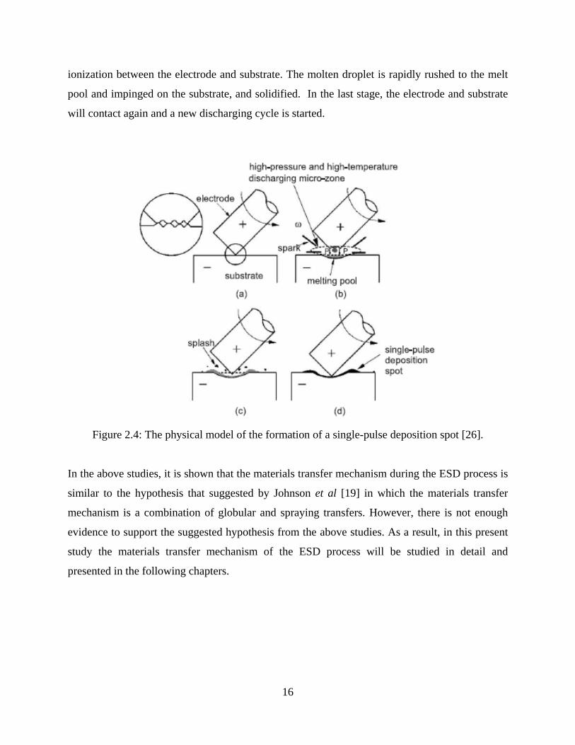
16
ionization between the electrode and substrate. The molten droplet is rapidly rushed to the melt
pool and impinged on the substrate, and solidified. In the last stage, the electrode and substrate
will contact again and a new discharging cycle is started.
Figure 2.4: The physical model of the formation of a single-pulse deposition spot [26].
In the above studies, it is shown that the materials transfer mechanism during the ESD process is
similar to the hypothesis that suggested by Johnson et al [19] in which the materials transfer
mechanism is a combination of globular and spraying transfers. However, there is not enough
evidence to support the suggested hypothesis from the above studies. As a result, in this present
study the materials transfer mechanism of the ESD process will be studied in detail and
presented in the following chapters.
17
2.5 ESD Application and Performance The first application of the ESD process was the formation of martensite by sparking between a
steel electrode and a steel substrate to form a hard facing coating [8]. The most common
applications of the ESD process are to apply wear resistance and corrosion resistance coating.
The continuous development of the ESD process has led to many other industrial applications. In
the following, some of the industrial applications and the performance of the ESD coating will be
reviewed.
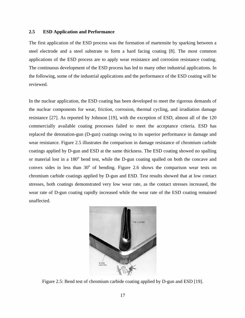
In the nuclear application, the ESD coating has been developed to meet the rigorous demands of
the nuclear components for wear, friction, corrosion, thermal cycling, and irradiation damage
resistance [27]. As reported by Johnson [19], with the exception of ESD, almost all of the 120
commercially available coating processes failed to meet the acceptance criteria. ESD has
replaced the detonation-gun (D-gun) coatings owing to its superior performance in damage and
wear resistance. Figure 2.5 illustrates the comparison in damage resistance of chromium carbide
coatings applied by D-gun and ESD at the same thickness. The ESD coating showed no spalling
or material lost in a 180o bend test, while the D-gun coating spalled on both the concave and
convex sides in less than 30o of bending. Figure 2.6 shows the comparison wear tests on
chromium carbide coatings applied by D-gun and ESD. Test results showed that at low contact
stresses, both coatings demonstrated very low wear rate, as the contact stresses increased, the
wear rate of D-gun coating rapidly increased while the wear rate of the ESD coating remained
unaffected.
Figure 2.5: Bend test of chromium carbide coating applied by D-gun and ESD [19].

18
Figure 2.6: Effect of contact stress on wear of D-gun and ESD chromium carbide coating [19].
Figure 2.7: Friction of ESD and D-gun coatings in sodium [19].

19
The superior in both damage and wear resistance of the ESD coating is related to the structure
and bonding of the coating. ESD coating has much finer grain and homogeneous structure than
the D-gun coating because of the rapid solidification of ESD. Also, the ESD coating is
metallugically bonded to the substrate, while the D-gun coating is primarily mechanical bond
[19]. Furthermore, the ESD coating showed better performance in both friction and corrosion
performance as shown on Figure 2.7 and 2.8.
Figure 2.8: Corrosion performance of chromium carbide coatings in sodium at 625oC [19].
The ESD process is also widely used in the aerospace applications. ESD process provides
surface treatments for wear, erosion, and corrosion resistance as well as repair and recovery of
high values parts such as turbine components [19]. Examples of ESD in the aerospace
applications include hardsurfacing of blade tips and notches for wear control in ablative seals,
pre-placement of platinum on blades prior to platinum aluminide diffusion coating, repair of
casting defects, pre-placement of braze alloys on difficult-to-wet superalloys for precision
assembly of components, repair of diffusion coatings, build up and repair of worn or undersize
parts, coatings to resist particle erosion from ingestion of sand in military turbines and repair of
thermal fatigue cracks in single crystal turbine blades. Figure 2.9 shows the repairing of single
crystal turbine blade by ESD, where the low net heat input and free from distortion were
requirements for repairing singe crystal alloys [28].

20
(a) (b)
(c)
Figure 2.9: Repair of single crystal turbine blade by ESD: a) as-received blade with thermal fatigue cracks, b) cracks removed by grinding, c) restored by ESD using original materials as filler and finished. [28].
In addition, the ESD has also been used in automotive applications, where titanium carbide
coatings are deposited on the titanium valve stems and valve guides in the high performance
internal combustion engines [19]. Huys Industries Ltd. has developed and patented the TiCp/Ni
metal-matrix-composite (MMC) coating on resistance spot welding (RSW) copper electrode to
improve the electrode tip life in RSW of Zn-coated sheet steel. As Zn coating react with the Cu
electrode to form brass alloys during RSW, causing the local bonding between the electrode and
the sheet steel. Fracture of these local bonds will lead to material loss on the electrode surface
and causing the growth of the electrode tips diameter and eventually failure of the electrode.
Figure 2.10 illustrated that the electrode tip diameter growth rate is slower with the TiCp/Ni
coating when number of welds exceeded 100. Chen et al [3, 9] studied the TiCp/Ni MMC coating
deposited on the surface of the RSW Cu electrode by the ESD process. The coating successfully
acted as a barrier to prevent Cu from reacting with the Zn coating thereby improved the electrode
tip life [3].

21
Figure 2.10: Electrode tip growth diameter as a function of weld number [3].
Other industrial applications include replacing the expensive tungsten carbide brazed inserts tips
of surgical tools and needle holders with ESD chromium carbide coating. Coatings on the
orthopedic drills, dental tools, hemostats, and orthotic leg and ankle brace components for the
medical applications. For the high tech sports equipments, ESD coating is applied on knife edges,
knife sharpeners, golf clubs, ski edges, ice axes, and crampons [19].
2.6 ESD Process Improvement As stated above, the ESD process demonstrates some unique advantages over other coating
processes. However, there is a fundamental dilemma with ESD, which the process can only be
optimized for either quality or efficiency. As a result, improvement in deposition rate without
sacrificing the quality of the coating must be achieved through optimization of the process
parameters. There are several factors control the coating efficiency, such as the electrode
properties (melting point and heat capacities), environment, and the electrical characteristic
(spark energy and spark frequency) [8, 10, 18, 19]. The most important factor is the charge-
discharge frequency.

22
Several improvements in deposition rate are achieved through the advances in the design of
power supply. A capacitor discharge design is used by most of the conventional ESD power
supply (see Figure 2.11) and the discharge of the capacitor is often initiated by the contact of the
electrode and substrate [10]. For a vibrating applicator, the charge-discharge frequency is
determined by the vibration frequency of the electrode and the restriction of the mechanical
movement tends to have low deposition rate. If a rotational applicator is used, the irregular
contact between the electrode and substrate varies the discharge frequency and voltage, which
results in slow and unstable coating process. The discharge voltage can be increased by using a
silicon controlled rectifier (SCR). However, the inductor used to regulate short-circuiting
currents will extend the discharge duration and affect the discharge frequency [29].
Figure 2.11: Block diagram of conventional ESD equipments [29].
Figure 2.12: Block diagram of newly designed accelerated ESD power supply [29].
The new power supply design has taken the advantages of inverter-based electronic and
microprocessor control. Wang et al [29] have studied the ESD process by using the newly
designed power supply as shown on Figure 2.12. This new design utilizes the isolated gate

23
bipolar transistor (IGBT) switches coupled with controlling and the driving circuits. The
electrical pulse is obtained by utilizing one switch, IGBT1, to the charge circuit, and the other
switch, IGBT2, to the discharge circuit. The controlling and the driving circuits control the
ON/OFF states of the two switches. When the voltage reaches a reset level, IGBT1 will be off
and IGBT2 will be on and the capacitors will discharge. When the voltage drops to a lower level,
IGBT1 will be on and IGBT2 will be off and the capacitors charging cycle begins. The
advantages of IGBT switch are its flexibility and adjustability to the wide range of voltage and
current. This allows higher charging voltage with short pulse period and increase in spark
frequency [29]. It is shown in Table 2.4 that the both the coating thickness and deposition rate
are increased by using the newly designed ESD power supply.
Table 2.4: Comparison between the conventional and newly designed ESD power supply [29]. Conventional New
Power supply, V 220, single phase 220, single phase Higest output Voltage, V 40 – 50 30 – 75 Operating current, A 1 – 3 <10 Maximum coating thickness, µm 50 – 60 100 Roughness, µm 1.6 – 6.3 2.6 – 6.3 Coating rate(a), mm2/s 0.5 – 0.8 1.6 – 3.2 (a) For highest coating thickness
2.7 Summary In this chapter, the ESD historical background, process characteristic, applications, performance
and process improvement development have been reviewed. The Electro-Spark Deposition is a
micro-bonding process, in which short duration pulses of current are used to bond the electrode
material to a metallic substrate. The process was first discovered in 1924 by H. S. Rawdon and
subsequently found many usages in various industries.
ESD possesses some unique advantages. The coating material is metallurgically bonded to the
substrate. The low net heat input allows the substrate to remain at ambient temperature during
the process, and the rapid solidification of the deposits produces a nano-structured or amorphous
structured coating. As a result, the most common application of the ESD process is to apply wear
resistance coating. However, there are some limitations to the ESD process, such as the low

24
coating efficiency, and the stress relief cracking inherent in some materials. The advantages and
limitations of the ESD process are summarized in Table 2.5.
The mechanism of material transfer from the electrode to the substrate during ESD process is
generally not well understood. It has been suggested that the coating material is transferred
through solid, liquid, or gaseous state. Others suggest that the transfer mechanism is similar to
those found in GMAW process. Generally, further experimental study is required to understand
the material transfer mechanism during the ESD process.
There is a fundamental dilemma with the ESD process, which it can only be optimized for either
quality or efficiency. Improvements in deposition rate have been achieved by advances in power
supply design. The new power supplies use SCR control for higher discharge voltage and IGBT
switching for higher discharge frequencies. And it is found that the both coating thickness and
coating efficiency are improved by using the new power supply design.
The literature studies presented above showed that limited works have been done on studying the
effects of ESD parameter interactions on coating quality. Also, there is not enough evident to
support and detail the materials transfer mechanism during the ESD process. As a result, the
objective of the present study is to enhance the current understanding to the ESD process by
using a single deposition study. The ESD parameter interactions on coating quality, materials
transfer and bonding mechanism will be addressed and discussed in the following chapters.

25
Table 2.5 Summary of the advantages and limitation of the ESD process [8]. Advantages Limitations
Metallurgically bonded coating Maximum coating thickness of currently 50 to
250 µm, depending on material Low heat input, eliminates distortion or
metallurgical changes in substrate Stress relief cracking inherent in some
materials Nano-structured or amorphous layers possible
through rapid solidification Both substrate and coating material much be
electrically conductive Little or no substrate preparation or post-
coating surface finishing required Maximum effective coating rate of 20cm2/min
Reproducible process, easily automated Extensive optimization of coating parameters
may be required for some application Operators easily trained
Portable equipment and process Applicable to complex shapes
Can apply nearly all metals and cermets

26
Chapter 3 3 Experimental Methods In this chapter, the experimental equipment, materials and experimental methods are presented.
First, the major components and their functions of the electrospark deposition setup are
explained. Second, the materials used including the compositions and surface condition are
presented. Then, the experimental methods including sample preparation and material
characterization are detailed in the remaining sections of this chapter.
3.1 Equipment 3.1.1 Electro-Spark Deposition (ESD) Setup The ESD setup was designed and built at Center of Advance Materials Joining (CAMJ) at the
University of Waterloo. Figure 3.1 shows the ESD setup which consists of 3 major components;
Spring-loaded mechanical apparatus, ESD circuit, and Data acquisition (DAQ) system.
Figure 3.1: Electro-Spark Deposition setup
27
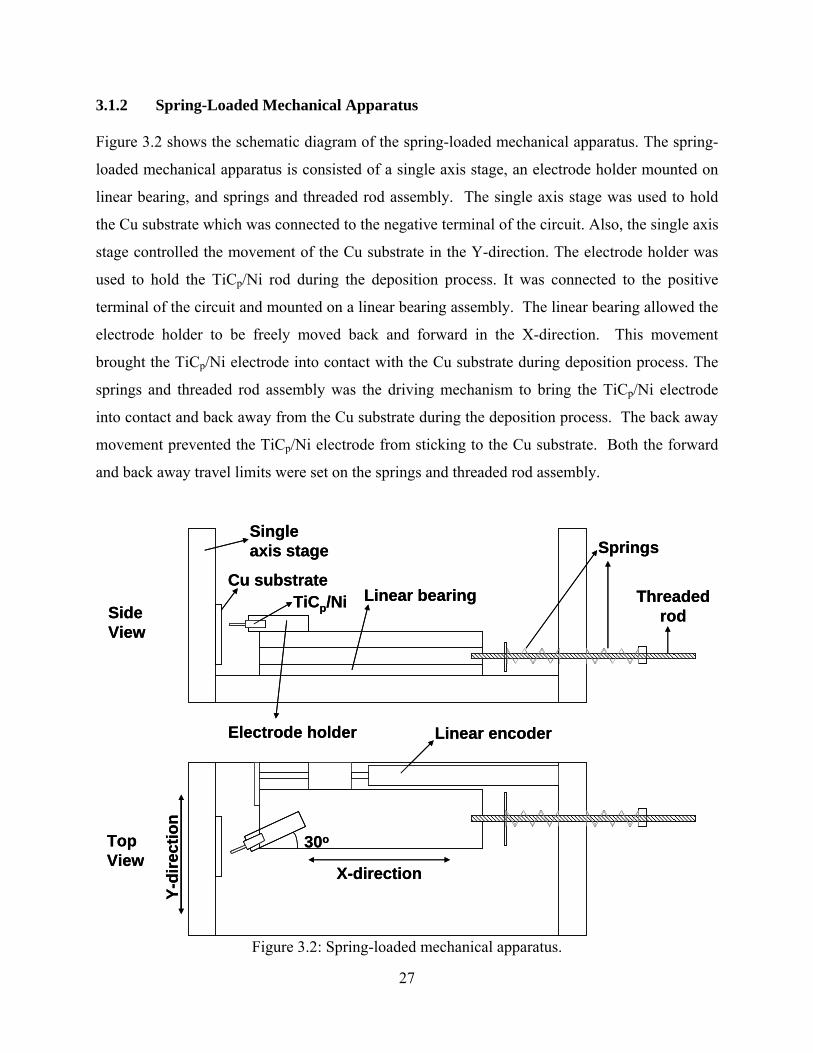
3.1.2 Spring-Loaded Mechanical Apparatus Figure 3.2 shows the schematic diagram of the spring-loaded mechanical apparatus. The spring-
loaded mechanical apparatus is consisted of a single axis stage, an electrode holder mounted on
linear bearing, and springs and threaded rod assembly. The single axis stage was used to hold
the Cu substrate which was connected to the negative terminal of the circuit. Also, the single axis
stage controlled the movement of the Cu substrate in the Y-direction. The electrode holder was
used to hold the TiCp/Ni rod during the deposition process. It was connected to the positive
terminal of the circuit and mounted on a linear bearing assembly. The linear bearing allowed the
electrode holder to be freely moved back and forward in the X-direction. This movement
brought the TiCp/Ni electrode into contact with the Cu substrate during deposition process. The
springs and threaded rod assembly was the driving mechanism to bring the TiCp/Ni electrode
into contact and back away from the Cu substrate during the deposition process. The back away
movement prevented the TiCp/Ni electrode from sticking to the Cu substrate. Both the forward
and back away travel limits were set on the springs and threaded rod assembly.
Threaded rodSide
View
Top View
Single axis stage
Cu substrateTiCp/Ni Linear bearing
Springs
30o
Linear encoderElectrode holder
Y-di
rect
ion
X-direction
Threaded rodSide
View
Top View
Single axis stage
Cu substrateTiCp/Ni Linear bearing
Springs
30o
Linear encoderElectrode holder
Y-di
rect
ion
X-direction
Figure 3.2: Spring-loaded mechanical apparatus.

28
Figure 3.3: An electrical schematic diagram showing the ESD circuit.
3.1.3 ESD Circuit Figure 3.3 shows a schematic electrical diagram of the ESD circuit. The ESD circuit is consisted
of two 1000μF capacitors, power supply or voltage source, a relay and a computer-controlled
driver circuit. The capacitors were used to store and to discharge the electrical power during the
deposition process. The power supply was an adjustable constant voltage power supply that
could charge up the capacitors to a preset voltage level. The relay was used to control whether
the ESD circuit would be in charge or discharge modes. This relay was controlled by a
computer-controlled driver circuit. In the present study, the ESD circuit was always set to
charge mode by default setting of the program. When ready, a command would be inserted into
the program to switch the relay into discharge mode.

29
Figure 3.4: Data acquisition system for the ESD.
3.1.4 Data Acquisition System (DAQ) Figure 3.4 shows a schematic diagram of the data acquisition system (DAQ) used in the present
study. Connected to a laptop, the DAQ system was consisted of a current and a voltage sensors, a
linear displacement encoder, a signal conditioning circuit board and a DAQ box. The system
was controlled using a program written in LabView. The current sensor was a magnetic coil
design that had ±0.001A resolution. The current sensor had a through hole which allowed the
power cable to pass through from the deposition electrode to the positive terminal on the ESD
power supply. The voltage reading device was a microchip that had ±0.1V resolution. The
voltage reading device was connected to both ends of the positive and negative terminals by
copper wires to measure the potential difference during the deposition process. The linear
displacement encoder was a Heidenhain MT 2571 length gauge with 100kS/s sampling rate and
±0.1um resolution. It was mounted to the moving stage of spring-loaded mechanical system as
shown on Figure 3.2 to measure displacement during the deposition process. The current and
voltage reading sensors were connected to the signal conditioning board to convert the signal
into appropriate format for the DAQ system. The DAQ box used in this study was a National
Instrument USB-6211 M Series Multifunction DAQ with 250 kS/s sampling rate. The computer
software used to collect all the measurement data was National Instrument LabView 8.6 (see
Appendix). The sampling rate was set to be 100kS/s per channel in this study.

30
Figure 3.5 shows the current, voltage and displacement data of a single ESD process. The linear
encoder was first set to the zero reference position along with the TiCp/Ni electrode. Then, it
was pull backward to a set position. As a result, the displacement data became negative.
Initially, the ESD circuit was set to the charge mode. As the TiCp/Ni electrode was traveling
towards the Cu substrate, however, the computer program switched the ESD circuit to discharge
mode. This was evident by the increase of the measured voltage to 35 V. Finally, the TiCp/Ni
contacted with Cu substrate and initiated the discharge.
Figure 3.5: DAQ output of a single ESD deposition
3.2 Material Characterization Apparatus In the present study, different material characterization apparatuses were used and they will be
described in the following sub-sections.
3.2.1 Microscopy Optical Microscope and Scanning Electron Microscope (SEM) were used to observe the surface
and the cross-section of the ESD deposition. The optical microscope used in this study was

31
Olympus BX51M System Metallurgical Microscope. On the other hand, SEM was performed
using a Jeol JSM 6460 with an attached Oxford Instruments INCA-350 for energy dispersive
spectroscopy (EDS) analysis.
3.2.2 Surface Analysis and Depth Measurement Surface analysis and depth measurement of the ESD single deposition were performed using a
WYKO NT1100 Optical Profiler. Data analysis was conducted using the Wyko Vision® analysis
software which accompanies with the Optical Profiler equipment. After scanning the surface of
the deposition spot, a 3D contour map was generated, and the data of the centre line of X and Y
profile were exported and plotted on Figures 3.6 a and b.
3.3.3 XRD Analysis XRD analysis was facilitated using a Rigaku MSC micro-XRD. For this particular XRD the Cu
k-alpha x-ray source is generated consisting of a 1.54 angstrom wavelength. A 0.8mm collimater
is used to focus on the surface of the ESD deposition spot. Data conditioning was conducted
using the JADE software which accompanies with the XRD equipment.
Figure 3.6a: X – profile surface scanning of single deposition.
32
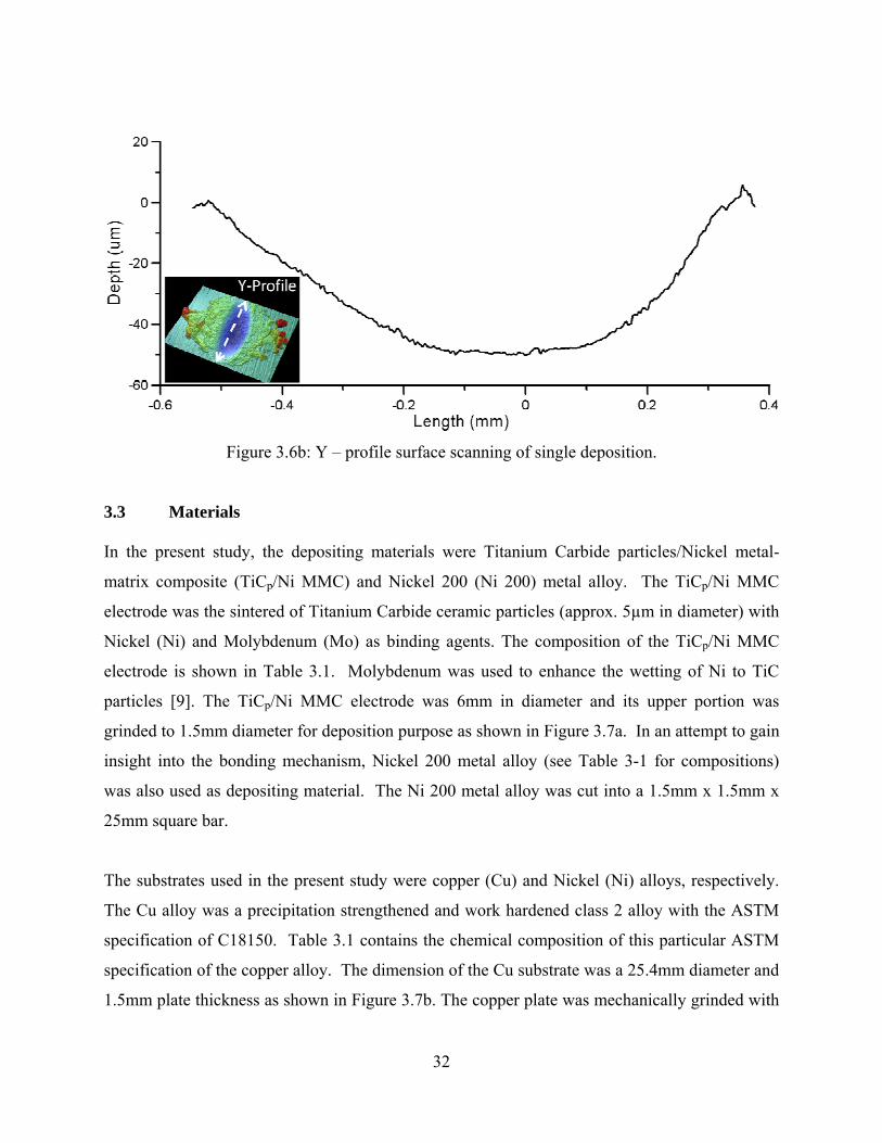
Figure 3.6b: Y – profile surface scanning of single deposition.
3.3 Materials In the present study, the depositing materials were Titanium Carbide particles/Nickel metal-
matrix composite (TiCp/Ni MMC) and Nickel 200 (Ni 200) metal alloy. The TiCp/Ni MMC
electrode was the sintered of Titanium Carbide ceramic particles (approx. 5µm in diameter) with
Nickel (Ni) and Molybdenum (Mo) as binding agents. The composition of the TiCp/Ni MMC
electrode is shown in Table 3.1. Molybdenum was used to enhance the wetting of Ni to TiC
particles [9]. The TiCp/Ni MMC electrode was 6mm in diameter and its upper portion was
grinded to 1.5mm diameter for deposition purpose as shown in Figure 3.7a. In an attempt to gain
insight into the bonding mechanism, Nickel 200 metal alloy (see Table 3-1 for compositions)
was also used as depositing material. The Ni 200 metal alloy was cut into a 1.5mm x 1.5mm x
25mm square bar.
The substrates used in the present study were copper (Cu) and Nickel (Ni) alloys, respectively.
The Cu alloy was a precipitation strengthened and work hardened class 2 alloy with the ASTM
specification of C18150. Table 3.1 contains the chemical composition of this particular ASTM
specification of the copper alloy. The dimension of the Cu substrate was a 25.4mm diameter and
1.5mm plate thickness as shown in Figure 3.7b. The copper plate was mechanically grinded with

33
320-grit SiC paper to remove oxide layer and washed with acetone before deposition. The Ni 200
substrate was cut into a 10mm x 10mm x 1.5 mm square plate. It was mechanically grinded with
320-grit SiC paper to remove oxide layer and washed with acetone prior deposition.
a) b)
Figure 3.7: Material used for ESD: a) TiCp/Ni depositing electrode b) Copper substrate.
Table 3.1: Compositions of depositing and substrate materials. Materials Composition (wt%) Ti Ni Mo W Cu Cr Zr C Mn S Si Fe TiCP/Ni MMC 68.36 15.44 13.40 2.80 - - - - - - - - Cu (C18150) - - - - 99.11 0.84 0.05 - - - - - Ni 200 - 99.00 - - 0.01 - - 0.35 0.25 0.01 0.35 0.4
3.4 Experimental Procedure
In the following sub-sections, the experimental procedure for different studies will be provided. 3.4.1 One ESD Deposition Study 3.4.1.1 Static Deposition Mode Testing Figure 3.8a shows the experimental setup used during the static deposition mode testing. The
TiCp/Ni MMC electrode was mounted on a second single axis stage which replaced the original
linear bearing and springs-threaded rod assembly. As a result, the TiCp/Ni MMC electrode was
manually moved toward the Cu substrate. The depositing electrode was set with an offset angle
of 30 degree. Figure 3.8b shows the close up image of the static deposition mode testing
apparatus. This setup allowed the formation of one ESD deposition while the location and the
movement of the electrode were strictly controlled.

34
To determine the occurrence of sparking between the electrode and the substrate, the TiCp/Ni
MMC electrode was incrementally moved towards the Cu substrate. After each move, the relay
was turned to discharge mode. If there was no spark, the relay was then switched back to charge
mode and the electrode was moved one more increment toward the Cu substrate. The distance,
at which a spark occurred, was recorded. It should be noted that no spark was formed until the
TiCp/Ni electrode touched the Cu substrate. The ESD deposition spot was then examined under
the SEM/EDS to observe the surface morphology and chemical analysis. Three samples were
made to prevent scattering of the result.
Figure 3.8a: ESD setup in Static mode.
Figure 3.8b: Close up image of the TiCp/Ni electrode and the Cu substrate.

35
3.4.1.2 Dynamic Deposition Mode Testing In dynamic deposition mode testing, the TiCp/Ni MMC electrode was mounted on the linear
bearing which was connected to springs-threaded rod assembly as shown in Figure 3.2. Unlike
the static mode, the springs-threaded rod assembly controlled the forward and back away
movement of the TiCp/Ni electrode.
Figure 3.9 shows the schematic diagram of the dynamic deposition mode process. The electrode
was initially pushed against Cu substrate. This location was referred to as the zero reference
point. Then, the TiCp/Ni electrode was pulled backward to a location previously set on the
springs-threaded rod assembly. At this time, the relay was switched to discharge mode and the
springs-threaded rod assembly was released. The previously compressed spring on one side of
the springs-threaded rod assembly sprang forward and brought the TiCp/Ni electrode into contact
with the Cu substrate. This initiated one ESD deposition. While the TiCp/Ni electrode was
moving toward the Cu substrate, a spring on the other side of the springs-threaded rod assembly
underwent a compression. This spring would be responsible for moving the TiCP/Ni electrode
back away from the Cu substrate after the discharge, to prevent the TiCp/Ni electrode from
bonding to the Cu substrate. Finally, the TiCp/Ni electrode returned to the original position. The
ESD deposition spot was then examined under the SEM/EDS to observe the surface morphology
and chemical analysis. Three samples were made to prevent scattering of the result.

36
Figure 3.9: Schematic diagram of the Dynamic Deposition Mode process.

37
3.4.2 The ESD Coating Interface Study Three different combinations of the coating and substrate materials were used to investigate the
ESD bonding mechanism, which are TiCp/Ni – Cu, TiCp/Ni – Ni, and Ni – Cu. The ESD
coatings were deposited using the spring-loaded mechanical apparatus. The ESD coatings
process was similar to the dynamic deposition mode testing, except the depositing electrode was
not pushed again the substrate initially. Eighty deposits on the same spot with each electrode-
substrate combination were made at 35V. The ESD coatings of each combination were examined
using XRD, and the cross-sections of coating-substrate were subjected to SEM/EDS analysis.
Three samples of each electrode-substrate combination were made to prevent scattering of the
result.
3.4.3 The ESD Coating Build-Up Study To document and to advance the current understanding of the coating build up during an ESD
process, an ESD coating build-up study was carried out. In this study, ESD coating was
performed on the substrate using the spring-loaded mechanical apparatus. The deposition
process was the same as described in the ESD bonding mechanism study. Figure 3.10 shows the
schematic diagram of the specimen. The ESD coating build-up study began with 1 ESD deposit
on the substrate. Then the ESD deposit was performed again at different locations on the
substrate, with the step increment of 1 deposit at a time on the same deposition spot, and up to 10
single deposits. It should be noted that the new edge of the TiCp/Ni electrode was used for the
ESD deposition at each deposition spot. The specimen was then examined under the SEM.
Figure 3.10: Schematic diagram of the specimen in coating build-up study. The numbers indicate
the number of ESD deposit.

38
3.4.4 The Effects of Voltage on ESD Process Study Single deposition was performed at 25V, 35V, 45V and 65V using the spring-loaded mechanical
apparatus to investigate the effects of voltage on ESD process. The deposition process was the
same as described in dynamic deposition mode testing. At each voltage level, ten samples were
made to provide statistically significance to the results. The samples were examined under the
SEM and Optical Profiler for surface analysis and depth measurement. To further evaluate the
effect of voltage on ESD coating, ten deposits were made on the same spot of Cu substrate using
the spring-loaded mechanical apparatus at each of the voltage levels. The specimens were cross-
sectioned and observed under the SEM.
3.4.5 Mass Gain and Loss Quantification Study In the mass gain and loss quantification study, the copper substrate was cut into 10mm × 10mm
× 0.8mm thin plate. Four different voltage levels (25V, 35V, 45V, 65V) were used to quantify
the mass gain and loss on both the TiCp/Ni electrode and Cu substrate. At each of the voltage
levels, 20, 40, 60, 80, and 100 ESD deposits were made using the spring-loaded mechanical
apparatus. The deposition process was the same as described in the ESD bonding mechanism
study. Both the TiCp/Ni electrode and copper substrate were weighted before and after
depositions using a Scientech SM124D analytical balance. This particular analytical balance has
the resolution up to 0.1mg. In order to achieve higher accuracy, the test samples were replicated
three times at each testing condition.

39
Chapter 4 4 ESD Process and Materials Transfer Mechanism
As stated in the literature review, several hypotheses to the material transfer mechanism during
the ESD process were proposed. However, not much work has been done to validate the
proposed hypotheses. As a result, the first step of the current study is to observe and document
the material transfer mechanism using experiments in which a single deposition was made. In
this chapter, the current, voltage and displacement data and the materials transferred during a
single deposition are presented and discussed. From the experimental observations, a
phenomenological model detailing the events taking place was developed. In addition, the
experimental observations were compared to similar phenomenon of other welding processes.
4.1 Static Deposition Mode
In static mode, the ESD single deposition was made by mounting the TiCp/Ni electrode on a
single axis stage as detailed in Chapter 3. The electrode was manually moved towards the copper
(Cu) substrate. In static mode, the electrode was held in place once it was moved to position.
After the TiCp/Ni electrode touched the Cu substrate, the ESD circuit was switched to discharge
mode to create one single deposition spot.
Figure 4.1 shows the SEM image of topographic morphology and accompanying EDS elemental
mapping of the ESD single deposition of TiCp/Ni on Cu substrate in static mode. In this instance,
35V was used. As evidenced in Figure 4.1, an elliptical crater was created at the centre of the
deposition area. The molten metal was expelled outward and re-solidified on the periphery of the
crater. Since the crater was elliptical, the expelled material was not distributed evenly around the
periphery. Also, a white region (indicated with the white dashed line) surrounding the crater of
the deposition is observed. This is possibly caused by the cathode pulverization that is often
observed in reversed polarity Gas Tungsten Arc Welding (GTAW) process to remove the surface
oxide film on the substrate during welding [26]. This observation indicates that ESD is a self-
cleaning process. In addition, the SEM/EDS elemental mapping shows that there is little
materials transfer between the TiCp/Ni electrode and the Cu substrate.

40
Figure 4.1: SEM image and EDS elemental mapping of ESD TiCp/Ni single deposition in static mode.

41
Figure 4.2 shows the SEM images of the corresponding TiCp/Ni depositing electrode after single
deposition in static mode. Solidification structure at the edge of the TiCp/Ni depositing electrode
suggests that melting of the TiCP/Ni electrode occurred during the deposition process. Although
the electrode was molten, as indicated in Figure 4.1, there is no evidence of TiCp/Ni deposited on
the Cu substrate.
Figure 4.2: SEM image of TiCp/Ni depositing electrode after single deposition in static mode. Figure 4.3 shows the variations of current and voltage as functions of time during single
deposition in static mode. The plot illustrates that the capacitors was partially discharged. The
voltage level dropped from the initial value of 35V to 18V. Meanwhile, the current suddenly
increased to 225A. After reaching the peak of 225A, the current rapidly declined back to 0A and
the voltage leveled out at 18V.
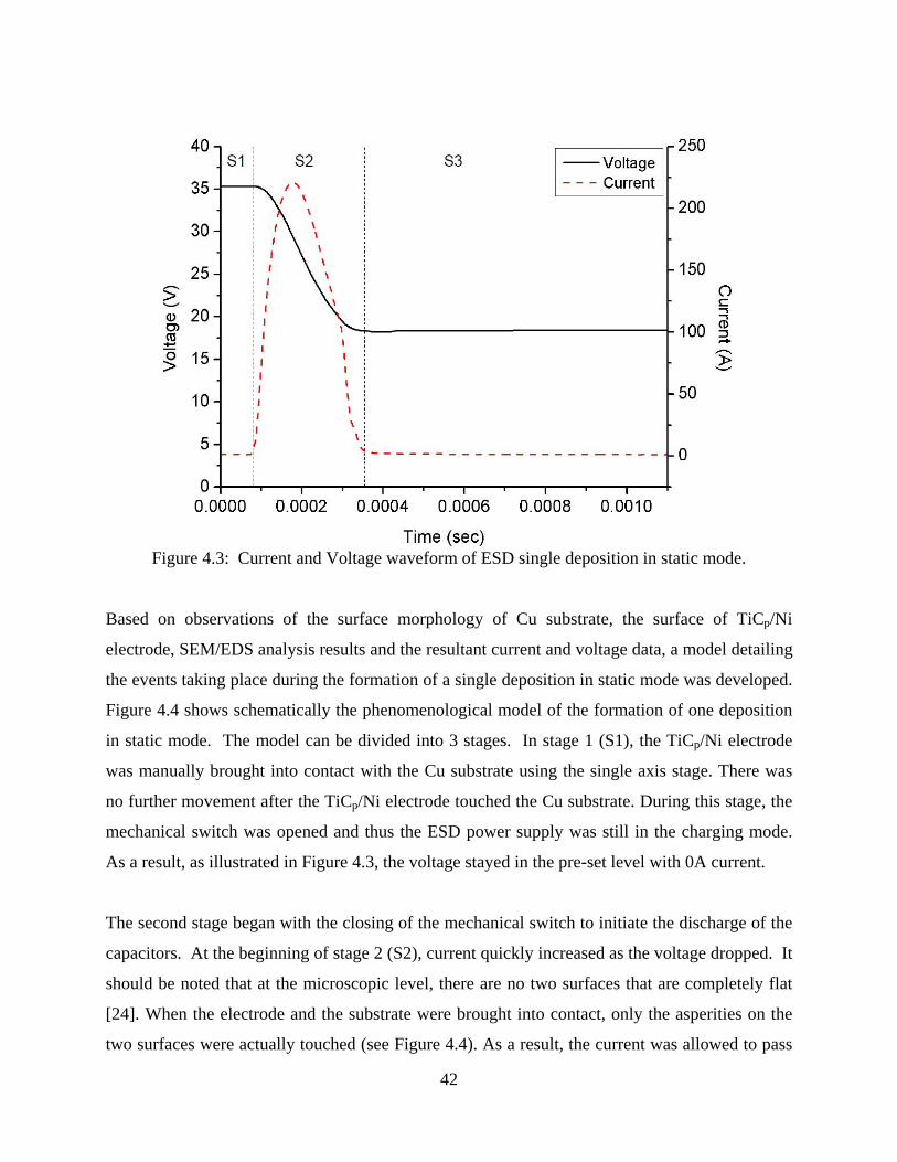
42
Figure 4.3: Current and Voltage waveform of ESD single deposition in static mode.
Based on observations of the surface morphology of Cu substrate, the surface of TiCp/Ni
electrode, SEM/EDS analysis results and the resultant current and voltage data, a model detailing
the events taking place during the formation of a single deposition in static mode was developed.
Figure 4.4 shows schematically the phenomenological model of the formation of one deposition
in static mode. The model can be divided into 3 stages. In stage 1 (S1), the TiCp/Ni electrode
was manually brought into contact with the Cu substrate using the single axis stage. There was
no further movement after the TiCp/Ni electrode touched the Cu substrate. During this stage, the
mechanical switch was opened and thus the ESD power supply was still in the charging mode.
As a result, as illustrated in Figure 4.3, the voltage stayed in the pre-set level with 0A current.
The second stage began with the closing of the mechanical switch to initiate the discharge of the
capacitors. At the beginning of stage 2 (S2), current quickly increased as the voltage dropped. It
should be noted that at the microscopic level, there are no two surfaces that are completely flat
[24]. When the electrode and the substrate were brought into contact, only the asperities on the
two surfaces were actually touched (see Figure 4.4). As a result, the current was allowed to pass

43
through these local contact points during discharge. The resistant heating (I2R) at these local
contact areas caused melting and vaporizing of the electrode and the substrate materials (see
Figure 4.2). In addition, because of the high current density at these local contact points, a spark
was initiated between the electrode and the substrate. The spark expelled the molten Cu
substrate forming a crater at the depositing location. A narrow gap was formed between the
electrode and substrate preventing further discharge of the capacitors in stage 3 (S3).
Figure 4.4: Phenomenological model of the formation of single deposition in static mode. From Figure 4.1, the surface appearance of deposition spot is different from the observations
reported by Liu et al [26]. In the latter case, the splash of the coating material was reported.
This splash appearance of the coating material was the result of the spraying and impinging of
molten coating droplets on the substrate surface [24, 28]. However, the crater appearance of the
deposition spot in the present study was caused by the ejection of molten substrate material [33 –
35]. Furthermore, there was little materials transfer between the TiCp/Ni electrode and the Cu
substrate. The materials transfer was caused by the condensation of the vaporized TiCp/Ni

44
electrode material on the Cu substrate. Based on this experimental observation, the spraying of
coating material to the substrate did not occur.
In conventional ESD process, the electrode is momentarily sticking to the substrate [26, 30]. In
the present study, the static mode did not mimic the ESD process entirely as the TiCp/Ni
electrode movement was restricted. As a result, to further examine the materials transfer
mechanism, the electrode movement was not restricted as detailed in the next section.
4.2 Dynamic Deposition Mode
In dynamic mode, the deposition was made using the spring-loaded mechanical system as
detailed in Chapter 3. The electrode was pulled back to a set position by the threaded rod. Upon
releasing of the threaded rod, TiCp/Ni electrode was brought into contact with the copper
substrate to initiate the discharge and one deposition was made. Unlike the static deposition
mode, the electrode was able to move further forward after the initial contact with the Cu
substrate.
Figure 4.5 shows the SEM image of topographic morphology and accompanying EDS elemental
mapping of one deposition of TiCP/Ni onto Cu substrate in dynamic mode. The deposition spot
had the same surface appearance as the static mode. An elliptical crater was created at the centre
of the deposition area and the expelled molten Cu substrate solidified along the minor axis of the
elliptical crater. A white region surrounding the crater was also observed. Unlike the static mode,
there was quantitative evidence of TiCp/Ni material transferred to the Cu substrate as shown on
the EDS elemental mappings of Figure 4.5. The single deposition consisted of the Cu substrate
and small amount of TiC and Ni. The electrode material was concentrated at the centre of the
deposition spot. Liu et al [26] measured the chemical composition across the single-pulse
deposition spots of four different coating – substrate couples. However, it is reported that the
content of the electrode materials was higher at the edge of the deposition spot than the centre of
the spot. Liu et al [26] believed that the lower electrode materials content at the centre of the
deposition spot is due to dilution by the substrate (see Figure 4.6). The discrepancy between the
literature and the present study will be explained in the later part of this section.

45
Figure 4.5: SEM image and EDS elemental mapping of ESD TiCp/Ni single deposition in
dynamic mode.

46
Figure 4.6: The composition of the electrode elements at different locations. On the left is the
data of Liu et al [26] and on the right is the data from the present study.
Figure 4.7 shows the SEM images of the TiCp/Ni electrode after one deposition in dynamic mode.
A molten structure was evident at the edge of the TiCp/Ni depositing electrode. In addition,
copper was found at the edge of the molten area on TiCp/Ni electrode. In fact, SEM/EDS
elemental mapping shows the presence of copper at both the top and bottom of the depositing
area on the TiCp/Ni electrode. The observation indicates that copper was picked up during the
deposition process.
Figure 4.7: SEM image and EDS elemental mapping of TiCp/Ni depositing electrode after single deposition in dynamic mode.
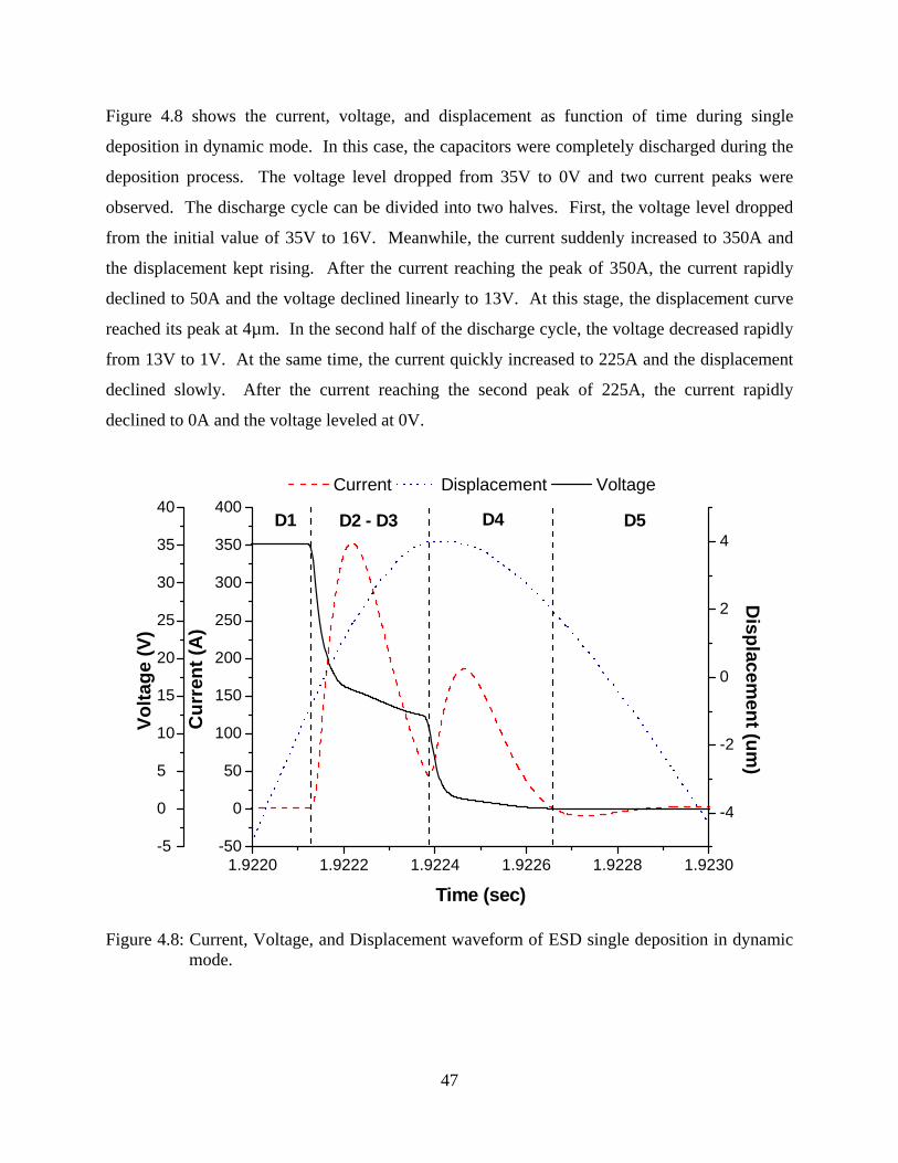
47
Figure 4.8 shows the current, voltage, and displacement as function of time during single
deposition in dynamic mode. In this case, the capacitors were completely discharged during the
deposition process. The voltage level dropped from 35V to 0V and two current peaks were
observed. The discharge cycle can be divided into two halves. First, the voltage level dropped
from the initial value of 35V to 16V. Meanwhile, the current suddenly increased to 350A and
the displacement kept rising. After the current reaching the peak of 350A, the current rapidly
declined to 50A and the voltage declined linearly to 13V. At this stage, the displacement curve
reached its peak at 4µm. In the second half of the discharge cycle, the voltage decreased rapidly
from 13V to 1V. At the same time, the current quickly increased to 225A and the displacement
declined slowly. After the current reaching the second peak of 225A, the current rapidly
declined to 0A and the voltage leveled at 0V.
-5
0
5
10
15
20
25
30
35
40
1.9220 1.9222 1.9224 1.9226 1.9228 1.9230-50
0
50
100
150
200
250
300
350
400 Current Displacement Voltage
Time (sec)
D1 D2 - D3 D4 D5
-4
-2
0
2
4
Volta
ge (V
)D
isplacement (um
)
Cur
rent
(A)
Figure 4.8: Current, Voltage, and Displacement waveform of ESD single deposition in dynamic mode.

48
A phenomenological model was developed for the dynamic deposition mode based on the above
observations. Figure 4.9 shows the model of the formation of one deposition in dynamic mode.
This model can be divided into 4 stages.
In stage 1 (D1), the depositing electrode was traveling towards to the substrate as indicated by
the increase in the displacement curve on Figure 4.8. At this point, no physical contact was made
between the electrode and the substrate. Thus, there was no current flow at this moment and the
voltage stayed at the pre-set level of 35V. In stage 2 (D2 – D3), the depositing electrode was
brought to contact with the substrate initiating the discharge. Voltage started to drop rapidly and
gave rise to the first current peak. Similar to the static mode, both the electrode and substrate
material were rapidly heated and melt at the local contact area. This leaded to the formation of
melt pool on the substrate and the thin film of molten materials on the electrode surface. After a
violent ejection of the molten substrate material, there was a momentarily gap between the
electrode and the substrate. As a result, current started to decline. However, the continuous
forward motion of the electrode caused it to contact the substrate again in stage 3 (D4). As it is
evidenced from the displacement curve (see Figure 4.8), the displacement of the TiCp/Ni
electrode reached its peak at this stage. Meanwhile, materials transfer occurred between the
electrode and substrate by direct contact of molten metal to molten metal. The thin film of
molten materials of both the electrode and substrate fused and mixed together through physical
contact. The electrode materials were deposited and solidified on the substrate at the points of
contact. Moreover, during the materials transfer, part of the molten substrate material (Cu) was
adhered and solidified on the electrode surface as shown on Figure 4.7. This is due to molten
substrate was ejected to the edge of the crater. Meanwhile, the capacitors discharged the
remaining energy and created the second current peak. In the last stage (D5), the TiCp/Ni
electrode was retracted to prevent the local bonding between the Cu substrate and the TiCp/Ni
electrode. Finally, the TiCp/Ni electrode returned to its original position for subsequent
depositions.

49
Figure 4.9: Phenomenological model of the formation of single deposition in dynamic mode.
As mentioned previously, Liu et al [26] reported that the content of the electrode material was
higher at the edge than at the centre of the deposition spot (see Figure 4.6). However, in the
present study, the content of the electrode materials was much more concentrated at the centre of
the deposition crater. The discrepancy between the literature and present study can be explained
by examining the material transfer mechanism. In literature, it was suggested that a molten
droplet and molten pool were formed on the electrode and substrate, respectively. The molten
droplet detached from the electrode surface and impinged to the molten pool on the substrate by
spraying [26, 30]. The deposited electrode materials content was diluted by the molten substrate
during the deposition process. This resulted in higher electrode contents at the edge of the
deposition spot. However, in the present study, molten droplet was not observed on the electrode
surface and the spraying mode of materials transfer did not occur as evidenced in the static mode
deposition. According to the above phenomenological model, the materials transfer mechanism
between the electrode and the substrate was primarily through direct molten metal to molten

50
metal contact. This is similar to the hypothesis suggested by Galinov et al [22]. Galinov et al
[22] proposed that the molten material on the electrode surface was partly driven away and
adhered to the substrate surface. Since the material transfer was through the physical contact
between the electrode and the substrate at the centre of the deposition crater, the content of the
electrode material was expectedly concentrated at the centre of the deposition spot.
4.3 Comparison of ESD to Other Joining and Welding Processes
In the previous sections, the surface morphology, the materials transfer mechanism and
phenomenological model detailing the events taking place during one deposition have been
presented and discussed. In the present study, ESD is viewed as a coating process. However,
Electro-Spark Deposition (ESD) is often described as a pulsed-arc microwelding process [22, 26,
30]. Therefore, a comparison between ESD and other joining or welding processes was
performed.
There are many differences between the ESD and commonly used arc welding processes. For
instance, the spark will ignite and extinguish alternately during the ESD process. However, the
arc will burn continuously throughout the entire arc welding process [25]. The depositing
electrode will be momentarily striking the surface of the substrate in the ESD process, while in
the arc welding process, there will be no physical contact between the electrode and the substrate
as soon as an arc is ignited. Furthermore, the electrode will be joined and broken away from the
substrate alternately due to the electrode motion in the ESD process, while in the arc welding
process, the electrode motion is not required.
As a result, it is inappropriate to describe the ESD process as an arc welding process. By
examining the voltage and current characteristic and the events taken place during one deposition,
the ESD process shows many similarities to the percussion and capacitor discharge welding.
These two welding processes belong to the family of resistance welding, in which resistance
heating and upset force are often used to join parts without filler metal [33 – 35, 36 – 39].

51
The principles of the aforementioned welding processes (see Figure 4.10) are similar to the
proposed phenomenological model of dynamic mode. The parts to be joined or welded are
clamped to the fixtures that are connected to the power source. Then, one of the parts is moved
towards to the other, at the local points of contact, resistance heating occurs, the high current
density leads to rapid melting and vaporization of the metal at the faying surface, and minute arc
is ignited. A narrow opening is generated as the metal melts faster than the moving part towards
the other end. The arc is extinguished as the two parts are in contact again. Finally, a weld is
made by the application of upset force to bring the molten interfaces in full contact [33 – 35, 36 –
39].
Figure 4.10: Schematic diagram of Capacitor Discharge Welding process. A. cathode positioned
above anode; B. arc ignition at the welding top; C. plasma expulsion; D. ejection and condensation of plasma into small metal particles; E. Joint after electrode contact [33].
Another similarity of the ESD process to the aforementioned welding processes is the electrical
characteristic. Both percussion and capacitor discharge welding use the capacitors as the power
source. A typical current pulse of percussion welding is shown on Figure 4.11, which illustrates
the two current peaks profile, and matches with the electrical characteristic in the present study.
The similarity in the electrical characteristic is attributed to the principle of the welding process
mentioned previously. When the parts to be joined are sufficiently separated, there is no current
flow, and then the current increase rapidly upon contact and melting of the materials occurs. The
decrease in current flow is associated with the narrow opening as the metal melts faster than the
moving part, and finally the materials engage, and shorting occurs with corresponding increase
in current flow. However, there is dissimilarity between the ESD process to the percussion and

52
capacitor discharge welding process. Owning to the electrode motion that requires to avoid
welding the electrode to the substrate in the ESD process, the electrode will never be joined
permanently to the substrate.
Based on the similarities and dissimilarities of the ESD process to the existing welding processes,
it can be concluded that the ESD process is more similar to the percussion and capacitor
discharge welding process than the arc welding process.
Figure 4.11: Current pulse of percussion welding [19].
4.4 Summary
In this chapter, static and dynamic deposition modes were performed to study the formation of
one deposition and the material transfer mechanism during ESD process. Based on the
experimental observations of the surface characteristic of one deposition, the electrode surface
and the chemical analysis, the coating material was transferred to the substrate through direct
molten metal to molten metal contact. A phenomenological model detailing the events taken
place during of the formation of one ESD deposition was developed for the each deposition
mode. At the end, the proposed model in the present work is used to compare the similar and
dissimilar phenomena to the existing welding processes. The ESD process is more similar to the
percussion and capacitor discharge welding process than the arc welding process.

53
Chapter 5 5 ESD process characteristic and Coating Evolution 5.1 Process parameter: Effect of Voltage on Electro-Spark Deposition ESD coatings were deposited using various voltage levels ranging from 25V to 65V to study the
effect of voltage on ESD. Since the previous studies only focused on the materials combinations
and coating performance, limited work have been done to correlate the applied voltage to the
resultant coating characteristic. The average length, width, crater depth, the cross-section of the
ESD coating at different voltage levels, the materials transfer trend and efficiency at different
voltage levels will be addressed and discussed in this section.
5.1.1 ESD Equipment Characteristic The ESD circuitry used in this study was designed and built at the UW CAMJ laboratory as
described previously in Chapter 3. Figure 5.1 shows the current and voltage as functions of time
during single deposition at 25V, 35V, and 45V, respectively. All three current and voltage
waveforms profiles show many similarities. The voltage first was decreased sharply to 16V,
linearly declined to 13V and finally dropped to 0V. In all cases, two current peaks were
observed and the total discharge cycle was approximately 400µs. The characteristic of these
electrical discharge profiles was detailed and discussed in Chapter 4.
In the present study, the ESD circuitry was a simple resistor capacitor (RC) circuit, which was
driven by a constant voltage source power supply [40]. When discharging the capacitors, the
out-flowing current of the capacitor must equal to the in-flowing current as described by
Kirchhoff’s current law [40]. The governing differential equation of this relationship is:
0=+CV
dtdVR (5.1)
where, R is the resistance, V is the voltage, C is the capacitance of the capacitor, and t is the
discharging time. The solution to the above differential equation is:

54
)/(0
RCteVV −= (5.2)
where V0 is the initial voltage of the capacitor prior to discharge and other variables are as
previously described. From the above equation, the capacitor’s voltage decreases exponentially
with time. The rate of discharge is governed by the capacitive time constant, τ = RC. As a result,
the discharging time is independent to amount of energy stored in the capacitors. This is in good
agreement with the observed data of the present study since the discharge was completed within
400 µs.
(a) (b)
(c)
Figure 5.1: Electrical Characteristic of single deposition for a) 25V, b) 35V, c) 45V applied voltage.
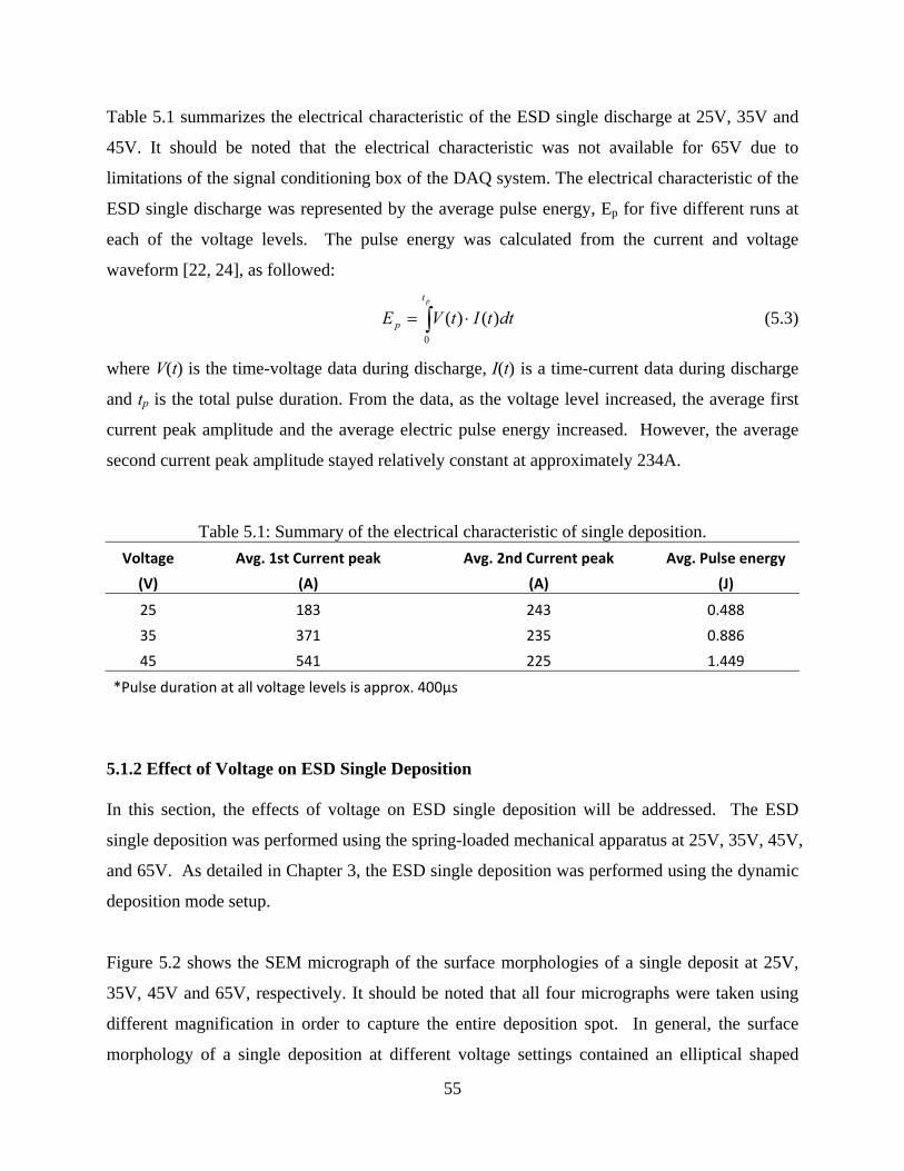
55
Table 5.1 summarizes the electrical characteristic of the ESD single discharge at 25V, 35V and
45V. It should be noted that the electrical characteristic was not available for 65V due to
limitations of the signal conditioning box of the DAQ system. The electrical characteristic of the
ESD single discharge was represented by the average pulse energy, Ep for five different runs at
each of the voltage levels. The pulse energy was calculated from the current and voltage
waveform [22, 24], as followed:
∫ ⋅=pt
p dttItVE0
)()( (5.3)
where V(t) is the time-voltage data during discharge, I(t) is a time-current data during discharge
and tp is the total pulse duration. From the data, as the voltage level increased, the average first
current peak amplitude and the average electric pulse energy increased. However, the average
second current peak amplitude stayed relatively constant at approximately 234A.
Table 5.1: Summary of the electrical characteristic of single deposition. Voltage Avg. 1st Current peak Avg. 2nd Current peak Avg. Pulse energy
(V) (A) (A) (J)
25 183 243 0.488
35 371 235 0.886
45 541 225 1.449
*Pulse duration at all voltage levels is approx. 400µs
5.1.2 Effect of Voltage on ESD Single Deposition In this section, the effects of voltage on ESD single deposition will be addressed. The ESD
single deposition was performed using the spring-loaded mechanical apparatus at 25V, 35V, 45V,
and 65V. As detailed in Chapter 3, the ESD single deposition was performed using the dynamic
deposition mode setup.
Figure 5.2 shows the SEM micrograph of the surface morphologies of a single deposit at 25V,
35V, 45V and 65V, respectively. It should be noted that all four micrographs were taken using
different magnification in order to capture the entire deposition spot. In general, the surface
morphology of a single deposition at different voltage settings contained an elliptical shaped
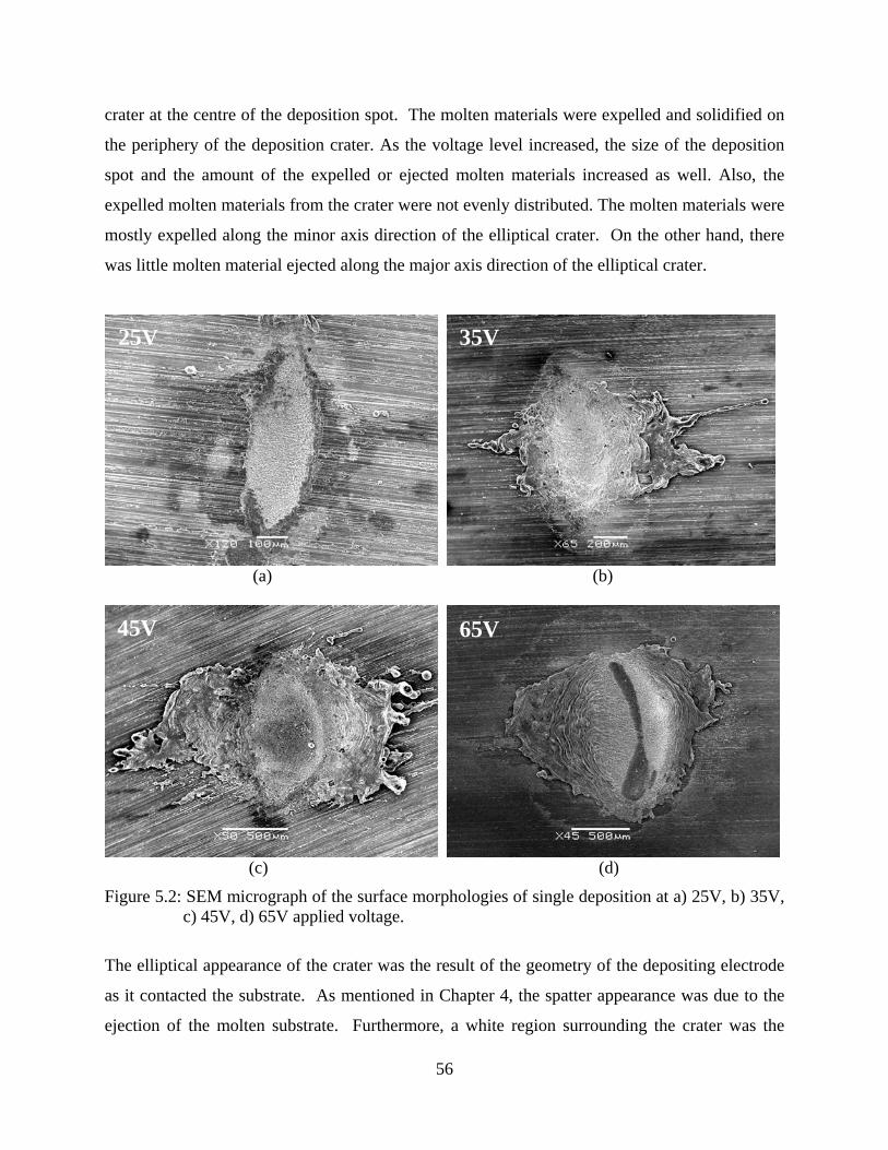
56
crater at the centre of the deposition spot. The molten materials were expelled and solidified on
the periphery of the deposition crater. As the voltage level increased, the size of the deposition
spot and the amount of the expelled or ejected molten materials increased as well. Also, the
expelled molten materials from the crater were not evenly distributed. The molten materials were
mostly expelled along the minor axis direction of the elliptical crater. On the other hand, there
was little molten material ejected along the major axis direction of the elliptical crater.
(a) (b)
(c) (d)
Figure 5.2: SEM micrograph of the surface morphologies of single deposition at a) 25V, b) 35V, c) 45V, d) 65V applied voltage.
The elliptical appearance of the crater was the result of the geometry of the depositing electrode
as it contacted the substrate. As mentioned in Chapter 4, the spatter appearance was due to the
ejection of the molten substrate. Furthermore, a white region surrounding the crater was the
25V 35V
45V 65V

57
result of cathode pulverization or the surface oxide cleaning action that was often observed in
reversed polarity GTAW [26].
The one dimensional contour profiles of the ESD single deposition at 25V, 35V, 45V and 65V
are shown in Figure 5.3. Each contour profile was scanned by the optical profiler along the x-
direction through the deepest point of the deposition spot. The scanning procedure was as
detailed in Chapter 3. In the present study, the original surface of the substrate was used as the
zero reference level which was represented by the horizontal dashed line in Figure 5.3. From the
contour profiles, as the voltage level increased, the depth and width of the crater increased and
more molten metal was thrown further away from the centre of the deposition spot.
In Table 5.1, as the applied voltage increased, the current flow in the system also increased. As
mentioned earlier, the heat generated during the ESD process is by resistant heating which is
proportional to the current flow (Q = I2R). As a result, the increase in current flow in the system
led to the increase in heat input and thus, the amount of the molten substrate and the size of the
crater.
In addition, during the deposition process, a spark was ignited. Burleigh and Eagar [41]
proposed that the arc force, F, can be mathematically expressed as:-
⎟⎟⎠
⎞⎜⎜⎝
⎛+=
1
22
ln218 R
RIF o
πμ
(5.4)
where I is the welding current, µ0 is the permeability of free space, R1 is the radius of the arc at
the welding electrode and R2 is the radius of the arc at the substrate. From the above equation,
the increase in the deposition current increases the corresponding arc force F. As a result, the
molten metal was expelled further away from the crater.

58
Figure 5.3: One dimensional contour profile (x-direction) of ESD single deposition.
25V
35V
45V
65V
Original surface
Original surface
Original surface
Original surface

59
5.1.3 Effect of Voltage on ESD Materials Transfer Figures 5.4a and 5.4b show the weight gained by the substrate and the weight lost by the TiCp/Ni
depositing electrode during the ESD process at different voltage settings. From the figures, the
Cu substrate weight gain increased as the voltage and the numbers of depositions increased. The
weight loss data shows the similar trend. The TiCp/Ni depositing electrode lost more as the
voltage and the numbers of depositions increased. Also, the TiCp/Ni weight loss was always
greater than Cu weight gain at all voltage levels. It is because not all the vaporized materials are
re-condensed on the surface of the substrate.
(a) (b) Figure 5.4: The weight gained by the Cu substrate (a) and the weight lost by the TiCp/Ni
depositing electrode (b) during the ESD process.
(a) (b)
Figure 5.5: Weight gain to loss ratio as a function of a) number of depositions and b) the applied voltage.

60
Figure 5.5a and 5.5b show ratio between the weight gained to the weight lost as a function of
number of depositions and voltage, respectively. This ratio can also be considered as the
efficiency of the ESD process. A high ratio implies that more weight was successfully
transferred to the substrate to form the coating than the weight lost by both the substrate and the
depositing electrode. Figure 5.5a shows that the weight gain to loss ratio increased with the
number of depositions for all voltage levels. However, in Figure 5.5b, the weight gain to loss
ratio decreased as the applied voltage increased.
In order to understand the effect of voltage on material transfer during the ESD process, the
theory of electrode erosion by electrical discharge should be re-visited. Galinov et al [22]
proposed that the electrode erosion by electrical discharge could be taken place in three distinct
phases: solid, liquid or vapour. The solid or vapour phase erosion of the electrode would lead to
a net loss while only the liquid phase had a positive net gain on materials transfer during the ESD
process. In solid phase erosion, the eroded solid particles by mechanical impact would not
adhere to either the electrode or the substrate surfaces. In vapour phase erosion, the vaporized
electrode and substrate materials mostly dissipated to the surrounding. Only small amount of the
vaporized materials were condensed and re-deposited on the substrate surface [42 – 46].
In liquid phase erosion, a portion of the molten electrode and molten substrate were coupled due
to the molten-metal to molten-metal contact and coating was formed on the substrate surface. In
this study, the molten-metal to molten-metal contact was clearly illustrated by the comparison
between the static and dynamic single deposition testing. As a result, in this study, the main
contribution to the Cu substrate weight gain was obtained through the TiCp/Ni liquid phase
erosion. Meanwhile, the TiCp/Ni electrode weight loss was mostly caused by liquid phase
erosion. However, since the electrode weight loss was always much greater than the substrate
weight gain, the TiCp/Ni electrode was also eroded by vapour and perhaps solid phase. In
addition, the three different phase erosion could also occur at Cu substrate. The Cu weight gain
was the net result of weight gain from the TiCp/Ni deposit minus the Cu weight loss.
Consequently, increasing the applied voltage did not necessary lead to the improvement of the
efficiency of the ESD process. It is because increasing the applied voltage did not only increase

61
the TiCp/Ni erosion, but also increased the Cu substrate erosion. Finally, it leads to the decrease
in the efficiency of materials transfer between the TiCp/Ni electrode and Cu substrate.
5.1.4 Effect of Voltage on ESD Coatings The ESD coatings at different applied voltages (25V, 35V, 45V, and 65V) were obtained by
having ten depositions at the same spot as detailed in Chapter 3. Figure 5.6 shows the SEM
micrographs of the cross-section of ESD coating after performing ten depositions at the same
location for different applied voltages. It should be noted that the SEM micrographs were taken
at different magnifications to obtain the overall cross-sectional view. In each SEM micrograph
of Figure 5.6, a continuous and dense coating was observed on the Cu substrate. The increased
applied voltage did not affect the overall coating thickness which apparently varied across the
entire spot. No delamination was observed between the coating and substrate at the centre of the
deposition spot. However, cracks and pores were observed within the coatings. The formation
of cracks within the coatings was caused by the repetitive mechanical impact and the thermal
stress relief cracking [47].

62
(a) (b)
(c) (d)
Figure 5.6: SEM micrograph of the cross-section of ESD coating at a) 25V, b) 35V, c) 45V, d) 65V applied voltage.

63
Figure 5.7a to Figure 5.7h show the edge and the center of the ESD coatings of Figure 5.6 using
higher magnification. By comparing these coatings, the cracks were found to be initiated from
the edge of the deposition crater and propagated underneath the coating to the Cu substrate. As
mentioned previously, there are no gaps or pores observed between the coatings and the substrate
at the centre of the deposition spot. It should be noted that the edge of the deposition crater was
where all the molten material were expelled to and re-solidified. At 25V (see Figures 5.7a and
5.7b), the crack initiated, but didn’t propagate very far into the Cu substrate. When the voltage
was set at 35V, the crack reached the centre of the deposition spot (see Figures 5.7c and 5.7d).
As the voltage was increased to 45V and later to 65V, the cracks size did not propagate very far
from the edge of the crater (see Figures 5.7e to 5.7h).
As discussed previously, ESD is a self-cleaning process in which the surface oxide film was
removed by catholic cleaning during electrical discharge. In addition, the spark expelled the
molten material outward from the center of the crater, thereby removing the molten contaminants
from the bonding surface. Previous studies have shown that surface contaminants and
cleanliness of the joining surfaces are crucial to the joint quality and the elimination of the joint
defects [22, 24, 26]. As a result, in Figures 5.7b, 5.7d, 5.7f and 5.7h, the TiCp/Ni coating bonded
well to the Cu substrate at the centre of the crater. As mentioned previously, cracks were
originated from the edge of the crater where the expelled molten materials along with the
contaminants were collected. As a result, bonding did not occur easily at the edge of the crater
and thus cracking could easily initiate. Furthermore, when the applied voltage was below 35V,
the arc force was not high enough to remove and to expel the surface contaminants away from
the bonding area. In these low voltage settings, cracks initiated and propagated at the Cu
substrate underneath the bonding interface. As the applied voltage increased, the resultant arc
force increased. This would expel more contaminant and thus better cleaning at the bonding
interface thereby preventing the crack from initiation and propagation.

64
Edge Centre 25
V
35V
45V
65V
Figure 5.7: SEM micrograph of cross-section of ESD coating at different applied voltage at higher magnification. a-b) 25V, c-d) 35V, e-f) 45V, g-h) 65V.

65
5.2 Evolution of the ESD Coating by Multi Deposits on the Same Spot In the previous discussion, this study has been focused on one deposit and the successive build
up of ESD coating has never been discussed. In this section, multiple deposits on the same spot
of the copper substrate were performed at 35V applied voltage. The spot would eventually have
up to 10 single deposits. Through the evolution of the multiple deposits on the same spot, the
ESD coating build up was studied.
Figure 5.8 a) to h) show the SEM topography micrograph of the first 8 TiCp/Ni multi-single
depositions on the same spot. Figure 5.8 i) to l) show the topography of the TiCp/Ni coating after
20, 40, 60, and 80 depositions on the same spot, respectively. As illustrated by the figures, the
deposition spot was progressively bigger and more TiCp/Ni material was deposited on the
substrate as the number of depositions increased. As the TiCp/Ni coating was building up, the
surface of the deposition spot was getting rougher. However, the deposited TiCp/Ni coating was
not evenly built across the entire deposition spot. It is also observed on Figure 5.8b that, not
much TiCp/Ni is deposited on the substrate; rather, the deposition spot illustrates the same
surface morphology as the single deposition.
As shown from the SEM micrographs, the ESD coating is the build up of the deposits by
depositing the TiC/Ni on the previous deposition spot. Initially, the first deposition is identical to
the single deposition described in the previous Chapter. In the latter case, a crater was formed at
the centre as the surface contaminant was removed from the deposition spot. The surface
morphology of the deposition spot changed from the crater to the typical splash appearance of
ESD coating [22, 24, 26] as shown on Figure 5.9a after three consecutive deposits. As the
coating continued to build up, the coating began to crack and propagate as shown on Figure 5.9b
and Figure 5.9c. A dense coating was formed but separated by cracks (see Figure 5.9d) and the
splash appearance was no longer observed.

66
(a) (b) (c) (d)
(e) (f) (g) (h)
(i) (j) (k) (l)
Figure 5.8: SEM micrograph of TiCp/Ni coating after: a) 1, b) 2, c) 3, d) 4, e) 5, f) 6, g) 7, h) 8, i) 20, j) 40, k) 60, and l) 80 deposits.
1 deposit 2 deposits 3 deposits 4 deposits
5 deposits 6 deposits 7 deposits 8 deposits
20 deposits 40 deposits 60 deposits 80 deposits

67
(a) – 3 deposits (b) – 4 deposits
(c) – 6 deposits (d) – 60 deposits
Figure 5.9: SEM micrograph of: a) 3, b) 4, c) 6, d) 60 deposits in higher magnification.
The change of the surface appearance of the coating during the deposition process was caused by
the continuous surface melting and surface erosion of both the TiCp/Ni electrode and the Cu
substrate. After the first deposition, the TiCp/Ni electrode was covered by a thin film of re-
solidified TiCp/Ni, and the deposition spot on the Cu substrate was covered by a thin layer of the
mixture of Cu and TiCp/Ni. As the deposition progressed, TiCp/Ni was deposited on top of the
pre-existing TiCp/Ni coating. Since the surface erosion of the TiCp/Ni electrode and coating
build up were irregular as shown in Figure 5.10. Local protuberances of deposits are formed on
both the depositing electrode and substrate surfaces. These protuberances on both surfaces will
serve as the contact points for subsequent depositions [8] resulting in uneven distribution of
TiCp/Ni coating across the deposition spot.

68
In addition, cracking of the TiCp/Ni coating was observed as the coating was built up. As
mentioned earlier, the formation of cracks was caused by the thermal stress built-up [47]. During
the deposition process, the molten TiCp/Ni was deposited on to the Cu substrate. Since substrate
was a greater heat sink due to the high thermal conductivity of copper, the molten TiCp/Ni
rapidly solidified and thus creating residual tensile thermal stress in the coating [47]. As the
deposition progressed, the build up of the thermal stress caused more cracks to nucleate and to
propagate within the brittle ceramic coating.
(a) (b)
Figure 5.10: SEM micrograph of: a) TiCp/Ni electrode after 10 deposits, b) TiCp/Ni coating after 10 deposits.

69
To further the understanding of the coating formation by the ESD process, TiCp/Ni and highly
pure Ni coatings were also deposited on Ni and Cu substrates respectively. Scanning Electron
Microscopy with Energy Dispersive Spectrometer (SEM/EDS) points scan and micro-X-ray
Diffraction (XRD) analyses were performed to characterize the coating-substrate interface.
0 5 10 15 20 25 30 35 40 45
0
20
40
60
80
100
Con
cent
ratio
n (w
t%.)
Measurement distance (um)
Ni Cu
Ni coating Cu substrateMixing zone
Scanning direction
Figure 5.11: Concentration profile of ESD Ni coating on Cu substrate.
The concentration profile of the Ni coating on Cu substrate is presented on Figure 5.11. A strong
and continuous interface was observed with the presence of the mixing zone between the Ni
coating and Cu substrate. The molten Cu and Ni mixed together to form an intermixing layer
during deposition process as predicted by the Cu-Ni binary phase diagram. As illustrated, the Cu
mixed much further into the Ni coating than the diffusion of Ni into the Cu substrate. On the Ni
coating side, the Cu content varied from 20 to 40 % wt with the Ni content made up the
remaining percentage. No nickel was found in the Cu substrate. The formation of the mixing
zone between the Ni coating and Cu substrate was the result of the rapid solidification of molten
Ni and Cu during the ESD process. Since the Cu substrate was a greater thermal mass, the heat
dissipated rapidly causing the molten Ni and Cu to quickly solidify. This result was similar that
observed by Dogan et al [48], in their study of capacitor discharge of Al-Fe couple. In their study,

70
Dogan et al [48] believes that a mixing zone of Al and Fe formed at the joint interface due to
rapid solidification.
Moreover, the Cu-Ni peaks were found on the x-ray diffraction (XRD) spectrum as shown on
Figure 5.12, which indicated the Cu-Ni solid solution was formed during coating process. The
Cu-Ni solid solution is formed by the intermixing of molten Cu and Ni. As illustrated on the Cu-
Ni phase diagram, Cu and Ni are completely soluble to each other at all concentration [49]. The
complete solubility of the Cu-Ni system is because of both Cu and Ni have the FCC crystal
structure, similar atomic radii (0.128nm for Cu and 0.125nm for Ni respectively) and
electronegativity (1.9 for Cu and 1.8 for Ni respectively), and finally the common in valences
(+1 for Cu and +2 for Ni respectively) [49]. The presence of the Cu-Ni phase in the Ni coating
evidenced the metallurgical bond between the coating and substrate. The metallurgical bonding
is attributed to the formation of solid solution.
Figure 5.12: XRD pattern of Ni coating on Cu substrate.

71
0 5 10 15 20 25 30 35 40 45
0
20
40
60
80
100
Mixing Zone
Con
cent
ratio
n (w
t%.)
Meausurement distance (um)
Ti Ni Cu Mo
TiCp/Ni Coating Cu Substrate
Scanning direction
Figure 5.13: Concentration profile of ESD TiCp/Ni coating on Cu substrate.
Based on the result of the ESD Ni coating on Cu substrate, it is expected that similar
phenomenon will be observed for the TiCp/Ni coating on Cu substrate. Although, an intermixing
layer was not found and only a continuous bonded interface was observed between the TiCp/Ni
coating and Cu substrate. A mixing zone is found within the coating close to the bonded
interface. As shown on Figure 5.13, the concentration profile of TiCp/Ni coating on Cu substrate
shows that the Ni content remained constant while the Cu content varied from 0 to 20 %wt
within the coating close to the bonded interface. This evidence indicates the infiltration of molten
Cu into the deposited layer. Note that both Ni and Ti content were not found in the Cu substrate,
which is similar to the previous case. Moreover, the Mo content remained constant within the
coating and the Ti content decreased from 80 wt-% to 50 wt-% within the transition zone.
TiCp/Ni coating was deposited on the Ni substrate using the same apparatus and parameters as in
the previous cases. From Figure 5.14, a continuous bonding interface was observed similar to
the observation from the TiCp/Ni coating on Cu substrate. In addition, significant amount of Ni
from the Ni substrate was mixed in to the coating as the Ni content varied from 16 to 50 wt-%

72
within the mixing zone. The TiCp/Ni depositing electrode was produced by liquid phase
sintering process of TiC particles with Ni and Mo as the binders. The Mo additive is to enhance
the wettability of Ni to TiC particles [9]. Since the Ni is used as the binding agent for TiC, it is
not available to mix with the molten Cu during the coating process as in the case of Ni coating to
Cu substrate.
The presence of Cu and Ni content within the TiCp/Ni coatings near the bonded interface suggest
that both Cu and Ni were mixed into the coating by capillary action during the ESD process as
molten metal was more mobile in a metal – ceramic mixture [51]. There was a possibility of the
formation of Cu – Ti and Ni – Ti intermetallic phases. In the XRD spectrum of Figure 5.15, the
main constitutes of TiCp/Ni coatings are Cu, Ni, and TiC and there are no peak of any
intermetallic phase. Since TiC is the most thermodynamically stable phase in the coating [52],
the mixing of Cu and Ni in the TiC/Ni coating is mostly mechanical.
0 5 10 15 20 25 30 35 40 45
0
20
40
60
80
100
Mixing ZoneTiCp/Ni Coating
Con
cent
ratio
n (w
t%)
Measurement distance (um)
Ti Ni Mo
Ni Substrate
Scanning direction
Figure 5.14: Concentration profile of ESD TiCp/Ni coating on Ni substrate.
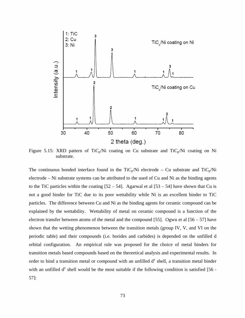
73
Figure 5.15: XRD pattern of TiCp/Ni coating on Cu substrate and TiCp/Ni coating on Ni
substrate.
The continuous bonded interface found in the TiCp/Ni electrode – Cu substrate and TiCp/Ni
electrode – Ni substrate systems can be attributed to the used of Cu and Ni as the binding agents
to the TiC particles within the coating [52 – 54]. Agarwal et al [53 – 54] have shown that Cu is
not a good binder for TiC due to its poor wettability while Ni is an excellent binder to TiC
particles. The difference between Cu and Ni as the binding agents for ceramic compound can be
explained by the wettability. Wettability of metal on ceramic compound is a function of the
electron transfer between atoms of the metal and the compound [55]. Ogwu et al [56 – 57] have
shown that the wetting phenomenon between the transition metals (group IV, V, and VI on the
periodic table) and their compounds (i.e. borides and carbides) is depended on the unfilled d
orbital configuration. An empirical rule was proposed for the choice of metal binders for
transition metals based compounds based on the theoretical analysis and experimental results. In
order to bind a transition metal or compound with an unfilled dx shell, a transition metal binder
with an unfilled dy shell would be the most suitable if the following condition is satisfied [56 -
57]:

74
x + y = 11 (5.5)
where x and y represent the number of electrons in the unfilled d shells.
In the present study, Cu has completely filled d shells with the configuration of 3d10 and the
electron configuration of TiC is 3d2.27 as reported by Manninen et al [56]. Since the empirical
rule of Equation 5.5 is not satisfied, Cu is a poor binder for TiC particles. In the case of TiCp/Ni
electrode and Ni substrate system, Ni has the unfilled d shells with the configuration of 3d8. This
satisfies the empirical rule and as a result, there is good metallurgical bonding (see Figure 5.14).
In addition, the theoretical analysis suggests that delamination or interfacial de-cohesion will
occur between the TiCp/Ni coating and Cu substrate since Cu is a poor binder for TiC. However,
in the study of TiCp/Ni coating on Cu substrate, a continuous bonded interface is observed. The
variation between the theoretical analysis and the experimental observation can be explained by
presence of Ni in the TiCp/Ni depositing electrode. It is reported by Chrysanthou et al [52] and
Lu et al [59] that the addition of Ni to TiC – Cu system will enhance the wettability of Cu to TiC
particles. Thus, a continuous bonding interface was observed for the TiCp/Ni electrode and Cu
substrate.
5.3 Summary In this Chapter, the effect of voltage on ESD coating, the evolution of ESD coating, and the ESD
bonding mechanism have been studied and discussed. In the effect of voltage on ESD coating,
the increase in applied voltage improved the surface cleanliness and led to stronger bonding
interface. However, the increase in applied voltage will also lead to greater materials loss in the
Cu substrate due to greater surface erosion. From the study of multi-single depositions on the
same spot, the dense ESD coating is achieved by the build up of countless of single depositions
that overlapped each other. Based on the experimental studies, the bonding mechanism of ESD
process is material dependence. In the metal – metal system, a metallurgical bond is formed with
the evidence of the intermixing layer between the coating and substrate. However, in the
ceramic – metal system, the molten metal is mixed into the coating and served as the binding
agent to the ceramic particles.

75
Chapter 6 6 Conclusions and Recommendations In this chapter, major observations, results, conclusions and recommendations from the current
study will be summarized.
6.1 Conclusions 6.1.1 Formation of ESD Single Deposition and Material Transfer In this study, the formation of one coating deposition on the substrate and material transfer
mechanism from the electrode to the substrate during ESD process were investigated. From the
experimental observations, a phenomenological model was proposed to detail the events taken
place during the ESD process as summarized below:
1) Once the electrode contacted substrate, an electrical spark was formed due to the
extremely high current density at the local contact points. The spark melted both the
substrate and the electrode.
2) The formation of the crater at the centre of the deposition spot was caused by outward
expulsion of the molten substrate material. A very narrow gap was created between the
TiCp/Ni depositing electrode and the Cu substrate. At this stage, material transfer between
the depositing electrode and the substrate did not occur.
3) Since the electrode continued to move forward, it came into contact with the substrate a
second time. The material transfer between the depositing electrode and the substrate
initiated during this second molten metal to molten metal contact. The thin film of molten
TiCp/Ni fused with the melting pool on the Cu substrate, and rapidly solidified to form a
coating.

76
6.1.2 The Effects of Voltage on ESD Coating The effects of voltage on ESD coating were examined by using single and multi-single
depositions on the same location. Some key conclusions include:
1) The size and the depth of the crater increased with higher applied voltages. The high
applied voltage would increase both the current density and the arc force. As a result,
more of the substrate was melted and ejected away forming a larger deposition crater.
2) The higher applied voltages increased the amount of coating deposited on the substrate.
However, it didn’t necessarily improve the overall net efficiency of the ESD process.
Increase in voltage would also increase the erosion rate of the substrate as more of the
molten substrate material ejected away.
3) The ESD is a self-cleaning process as the surface contaminants and oxide layer were
ejected away along with the molten substrate material. The increase in applied voltage led
to the reduction in crack size at the coating and substrate interface. In fact, the increase in
applied voltage improved the bonding between the coating and the substrate by
effectively removing the surface contaminant.
6.1.3 ESD Coating Evolution By having multi-single depositions on the same spot, the build-up of ESD coating was
investigated. The major experimental observations and conclusions are:
1) The ESD coating was formed by the build-up from numerous single depositions. After
the first deposition, the TiCp/Ni electrode was covered by a thin film of re-solidified
metal. Meanwhile, the crater on the Cu substrate contained a mixed layer of Cu and
TiCp/Ni. As the deposition progressed, TiCp/Ni deposited on top of the pre-existing
TiCp/Ni coating.
2) The uneven distribution of TiCp/Ni deposit across the deposition location was caused by
the formation of protuberances on both the TiCp/Ni depositing electrode and disposition
surface. These protuberances served as the contact points for subsequent depositions.

77
The ESD coating bonding interface was investigated by using 3 different material combinations
of the coating and substrate material. The material combinations were Ni electrode – Cu
substrate, TiCp/Ni electrode and Ni substrate and TiCp/Ni electrode and Cu substrate. The major
observations and conclusions are:
1) In the Ni electrode – Cu substrate system, the SEM observations and the XRD patterns
showed a metallurgical bond between the deposited coating and the substrate. As
predicted by the Cu-Ni phase diagram, an intermixing layer of Ni – Cu solid solution was
clearly observed.
2) In TiCp/Ni – Cu and TiCp/Ni – Ni combinations, there was no intermixing layer between
the coating and the substrate. From the XRD pattern, there was no evidence of
intermetallic phases. The SEM/EDS analysis showed the mixing of substrate material
into the coating. As a result, in these systems, both Cu and Ni were behaved as the
binding agent with the TiC ceramic particles.
3) From the present study, the metallurgical bonding between the coating and the substrate
is the bonding mechanism of the ESD process. The formation of the metallurgical bond is
attributed to either the formation of intermixing layer/solid solution or the usage of
substrate material as the binding agent to the depositing material.

78
6.2 Recommendations In the present study, the temperature of the TiCp/Ni electrode increased during consecutive
depositions. Preliminary study has found that the amount of depositing material increased as the
temperature of the electrode increased. As a result, the temperature build up during the
deposition process should be studied to decipher the influences of temperature of depositing
electrode on ESD process.
In addition, the effect of percentage of deposition spot overlapping should be studied. Since
cracks between the coating and substrate are originated from the edge of the crater. This is
where the expelled molten materials along with the contaminants are collected. As a result, by
overlapping the deposition spot might help eliminating cracking between the coating and
substrate.

79
References [1] M.R. Finlay. “Resistance Spot Welding of Metallic Coated Steels and PVD Coated
Electrodes.” CRC Australia and WTIA, CRC No. 18, 1996. [2] R. Holiday, J.D. Parker, N.T. Williams. “Relative contribution of electrode tip growth
mechanism in spot welding zinc coated steels.” Welding in the world 37 (1996) pp. 186-193
[3] Z. Chen, and Y. Zhou, “Surface modification of resistance welding electrode by electro-
spark deposited composite coatings: Part II. Metallurgical behavior during welding,” Surf. Coat. Technol., 2006, 201, 2419-2430
[4] Welding Handbook, Vol. 3, 9th ed., American Welding Society, Miami, FL, 2007 pp. 367 –
419. [5] Rointan F. Bunshah, “Handbook of Deposition Technologies for Films and Coatings 2nd
Edition.” Noyes Publications, 1994, pp. 131 – 163. [6] K.R. Chan, N. Scotchmer, J. Zhao, and Y. Zhou. “Weldability Improvement Using Coated
Electrodes for RSW of HDG Steel.” SAE international, 2006 [7] Z. Chen, and Y. Zhou, “Surface modification of resistance welding electrode by electro-
spark deposited composite coatings: Part I. Coating characterization,” Surf. Coat. Technol., 2006, 201, 1503-1510
[8] R.N. Johnson and G.L. Sheldon. “Advances in the electrospark deposition coating
process.” J. Vac. Sci. Technol. A 4 (6): 2740 – 2746 [9] ASM handbook – Powder Metal Technologies and Applications, Vol. 7, 10th ed., ASM
Int’l, Materials Park, OH, 1993, pp. 978 [10] Welding Handbook, Vol. 3, 9th ed., American Welding Society, Miami, FL, 2007 pp. 598 –
602. [11] N.C. Welsh, “Frictional Heating and its Influence on the Wear of Steel,” J. Appl. Phys. 28,
960 (1957) [12] N.C. Welsh, “Surface Hardening of Non-ferrous Metals by Spark Discharge,” Nature 181,
1004 (1958) [13] N.C. Welsh, “Spark Hardening of Metals,” J. Inst. Met. 88, 103 (1959) [14] N.C. Welsh and P.E. Watts, “The Wear Resistance of Spark Hardened Surface,” Wear 5,
189 (1962)

80
[15] N.C. Welsh and P.E. Watts, “Spark Hardening of Cutting Tools: Austenite Formation and Edge Erosion,” J. Iron and Steel Inst. London 198, 30 (1961)
[16] B.R. Lazarenko and N.I. Lazarenko, Electric Erosion of Materials (Gasenergoizdat,
Moscow/Leningrad, 1944), No. 1 [17] A.U. Polyachenko, New methods of Electrical Working of Materials (Mashgiz, Moscow,
1955), p.352 [18] Reynolds, J.L., R. L. Holdren and L. E. Brown., “Electro-Spark Deposition,” Advanced
Materials and Process 161 no3. March 2003 [19] R.N. Johnson, “ElectroSpark Deposition: Principles and Applications,” 45th Annual
Technical Conference Proceedings (2002), Society of Vacuum Coaters, 87 – 92 [20] S.W. Banovic, J.N. DuPont, and A.R. Marder, “Iron Aluminide Weld Overlay Coatings for
Bolier Tube Protection in Coal-Fried Low Nox Boilers,” Proc. 11th Ann. Conf. on Fossil Energy Materials, CONF-9705115, US-DOE, p. 279, 1997
[21] C.A. Schuh, T.G. Nieh and T. Yamasaki, “Hall-Petch breakdown manifested in abrasive
wear resistance of nanocrystalline nickel,” Scripta Materialia, Vol 46 (10), May 2002, 735 – 740
[22] I.V. Galinov and R. B. Luban, “Mass Transfer Trends during Electro-spark Alloy,” Surf.
Coat. Technol., 1996, 79, 9-18 [23] R.J. Wang, Y.Y. Qian, and J. Liu, “Structural and interfacial analysis of WC92-Co8
coating deposited on titanium alloy by electrospark deposition,” Applied Surface Science 228 (2004) 405 – 409
[24] A. Lesnjak, and J. Tusek, Processes and properties of deposits in electrospark deposition,
Science and Technology of Welding and Joining, 7, 6, 2002, 391-396. [25] Welding Handbook, Vol.2 , 8th ed., American Welding Society, Miami, FL, 1991 pp. 110-
155. [26] J. Liu, R. Wang, and Y. Qian, “Formation of a single-pulse electrospark deposition spot.”
Surface and Coatings Technology, 200, 2005, 2433-2437. [27] R.N. Johnson, “Coatings for Fast Breeder Reactor Components,” Thin Solid Films, 118,
(1), p. 31, 1984 [28] R.N. Johnson, “Alternative Coatings for Wear and Corrosion: the Electrospark Deposition
Process,” Proc. AESF Conf. for Environmental Excellence. January 2002.

81
[29] P.Z. Wang, G.S. Pan, Y. Zhou, J.X. Qu, and H.S. Shao, “Accelerated Electrospark Deposition and the Wear Behavior of Coatings,” Journal of Materials Engineering and Performance, 6 (6): 780-784 (1997)
[30] R. Wang, Y. Qian, and J. Liu, Interface behavior study of WC92-Co8 coating produced by
electrospark deposition, Applied Surface Science, 240, 2005, 42-47. [31] R.D. Wilson and J. A. Hawk. “Rapid Solidification Joining using the Capacitor Discharge
Welding Process.” 1994 [32] J.W. Simmons and R.D. Wilson. “Joining of High-Nitrogen Stainless Steel by Capacitor
Discharge Welding.” Welding Journal 185 – 190; June 1996 [33] R.D. Wilson, J.R. Woodyard, Sr., And J. H. Devletian. “Capacitor Discharge Welding:
Analysis through Ultrahigh-Speed Photography.” Welding Journal 101-106; March 1993. [34] B.K. Paul, D.D. Wilson, E.McDowell, and J. Benjarattananon, “ Study of weld strength
variability for capacitor discharge welding process automation.” Science and Technology of welding and joining 2001 vol. 6 no. 2 109-115
[35] J.F. Lancaster, “The Physics of welding.” Pergamon Press,. 1984 [36] Welding Handbook, Vol. 3, 9th ed., American Welding Society, Miami, FL, 2007 pp. 74 –
105. [37] K.N. Petry et al., “Principles and practices in contact welding.” Welding Journal 49(2):
117-126; February 1970 [38] W.F. Savage, “Flash welding: the process and application.” Welding Journal 41 (3): 227-
237; March 1962 [39] J.F. Sullivan, and W.F. Savage, “Effect of phase control during flashing on flash weld
defects.” Welding Journal 50(5): 213s-221s; May 1971. [40] K. Cumings, P. W. Laws, E. F. Redish, and P.J. Cooney, Understanding Physics:
Capacitance, 799 – 829; John Wiley & Sons, Inc. 2004 [41] T.D. Burleigh and T.W Eagar, “Measurement of the Force Exerted by a Welding Arc,”
Metall. Trans A, 14 (1983), 1223-1224 [42] A.E. Gitlevich, V.V. Mikhailov, N.Y. Parkansky and V.M. Revutsky, Electrospark
Alloying of the Metallic Surfaces, Stiinca, Kishinev, 1985, 196pp. [43] G.V. Samsonov, A.D. Verkhoturov, G.A. Bovkun and V.S. Sichev, Electrospark Alloying
of the Metallic Surfaces, Naukova Dumka, Kiev, 1985, 219pp.

82
[44] G.A. Krasiuk, Investigation of the powders – electrospark treatment erosion products, Electrospark Treatment of Metals, Academy of Sciences Publication, Moscow, 1963, pp. 126-132.
[45] K.K. Namitokov, Electroerosion Phenomena, Energiya, Moscow, 1978, 456pp. [46] N. Parkansky, I.I. Beilis, L. Rapoport, R.L. Boxman, S. Goldsmith, and Yu. Rosenberg,
“Electrode erosion and coating properties in pulsed air arc deposition of WC-based hard alloys,” Surf. Coat. Technol., 105 (1998) 130-134
[47] N. Parkansky, R.L. Boxman, S. Goldsmith, Surf. Coat. Technol. 61 (1993) 268 [48] C.P. Dogan, R.D. Wilson, and J.A. Hawk., “CD Weld Interfacial Structure for Al-Fe Based
Couples.” Mat. Res. Soc. Symp. Proc. Vol. 314. (1993) pp. 169-175 [49] ASM handbook – Alloy Phase Diagrams, Vol. 3, 10th ed., ASM Int’l, Materials Park, OH,
1993 [50] W.D. Callister, “Fundamentals of Materials Science and Engineering”, John Wiley and
Sons Ltd, 2004 [51] J. T. Klomp, Designing interfaces for technological applications: ceramic-ceramic and
ceramic-metal joining, 127-144; 1989, New York, NY, Elsevier Applied Science [52] L. Lu, J.Y.H. Fuh, Z.D. Chen, C.C. Leong, Y.S. Wong, Mater, Res, Bull. 35 (2000) 1555. [53] A. Agarwal, N.B. Dahotre, T.S. Sudarshan, Surf. Eng. 15 (1999) 27. [54] A. Agarwal, N.B, Dahotre, Mater. Charact. 42 (1999) 31. [55] G. V. Samsonov, "Surface phenomena in melts and powder metallurgy processes" (Izd-vo
AN UkrSSR, Kiev,1960) p. 60. [56] A.A. Ogwu, T.J, Davies, Mater. Sci. Technol. 9 (1993) 213 [57] A.A. Ogwu, T.J, Davies, Scr. Mater. 40 (1999) 1377 [58] S. Manninen, and T. Paakkari, Bonding in titanium carbide: I. Experimental electron
momentum distributions in polycrystalline Ti and TiC, J. Phys. C: Solid State Phys., Vol. 9, 1976.
[59] A. Chrysanthou, and G. Erbaccio, Enhancing the dispersion of TiC in copper, Journal of
Materials Science Letters 15 (1996) 774 – 775.

83
Appendix A DAQ Programming for ESD Process In this section, the LabView 8.5 graphical programming that was used to collect during the ESD
process and the description to the programming are presented.
LabView Programming The following graphical programming illustrates how the current, voltage, and displacement data
are collected during the ESD process.
1. Two analog channgles are created to to collect current and voltage data, and one digital
channel is created to collect displacement data.
2. A count down clock is set to let the user to preapre for the deposition.
3. A sample clock is set to adjust the sampling rate of the DAQ box.
4. The program will start collecting data upon completion of countdown.
5. All data will be converted to appropiate format and outputed as a graph.
6. Meanwhile, the data is written and saved to a text file.

84

85

86

87
88

89
Appendix B Experimental Data This section presents the data obtained from the weight quantification study on TiC/Ni electrode
and Cu substrate. Experiments were conducted on four different voltage settings, 25V, 35V, 45V,
and 65V. In addition, 20, 40, 60, 80, and 100 multi deposits were performed at each of the
voltage settings, and the result are shown as follow.
TiCp/Ni Electrode Weight Loss
Table A.1: TiCp/Ni electrode weight loss at 25V No. of deposits Before (mg) After (mg) Net (mg) Average Standard deviation
20 2172.29 2172.06 0.23
20 2172.5 2172.05 0.45
20 2172.11 2172.05 0.06 0.247 0.196
40 1422.53 1422.44 0.09
40 2173.03 2172.65 0.38
40 2172.65 2172.18 0.47 0.313 0.199
60 2172.88 2172.73 0.15
60 2172.73 2172.05 0.68
60 2172.57 2172.29 0.28 0.370 0.276
80 1422.97 1422.53 0.44
80 1423.26 1423.07 0.19
80 1423.07 1422.53 0.54 0.390 0.180
100 1424.09 1423.81 0.28
100 1423.81 1423.34 0.47
100 1423.34 1422.97 0.37 0.373 0.095

90
Table A.2: TiCp/Ni electrode weight loss at 35V No. of deposits Before (mg) After (mg) Net (mg) Average Standard deviation
20 979.52 979.08 0.44
20 979.08 978.75 0.33
20 978.75 978.49 0.26 0.343 0.091
40 1627.7 1627.3 0.4
40 1627.5 1627.02 0.48
40 1627.02 1626.67 0.35 0.410 0.066
60 1425.39 1424.92 0.47
60 1424.92 1424.58 0.34
60 1424.58 1424.06 0.52 0.443 0.093
80 1446.98 1446.19 0.79
80 1446.19 1445.6 0.59
80 1445.6 1445.06 0.54 0.640 0.132
100 1427.63 1427.01 0.62
100 1427.01 1426.45 0.56
100 1426.45 1425.69 0.76 0.647 0.103
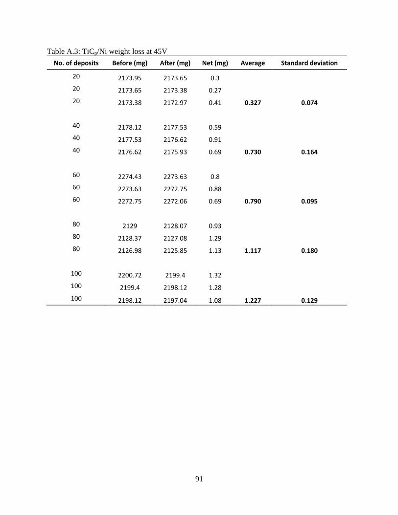
91
Table A.3: TiCp/Ni weight loss at 45V No. of deposits Before (mg) After (mg) Net (mg) Average Standard deviation
20 2173.95 2173.65 0.3
20 2173.65 2173.38 0.27
20 2173.38 2172.97 0.41 0.327 0.074
40 2178.12 2177.53 0.59
40 2177.53 2176.62 0.91
40 2176.62 2175.93 0.69 0.730 0.164
60 2274.43 2273.63 0.8
60 2273.63 2272.75 0.88
60 2272.75 2272.06 0.69 0.790 0.095
80 2129 2128.07 0.93
80 2128.37 2127.08 1.29
80 2126.98 2125.85 1.13 1.117 0.180
100 2200.72 2199.4 1.32
100 2199.4 2198.12 1.28
100 2198.12 2197.04 1.08 1.227 0.129

92
Table A.4: TiCp/Ni electrode weight loss at 65V No. of deposits Before (mg) After (mg) Net (mg) Average Standard deviation
20 1431.34 1430.84 0.5
20 1430.84 1430.6 0.24
20 1429.6 1429.26 0.34 0.360 0.131
40 1433.15 1432.45 0.7
40 1432.45 1431.91 0.54
40 1431.91 1431.34 0.57 0.603 0.085
60 1435.74 1434.81 0.93
60 1434.81 1434.15 0.66
60 1434.15 1433.15 1 0.863 0.180
80 1439.8 1438.57 1.23
80 1438.57 1437.04 1.53
80 1437.04 1435.74 1.3 1.353 0.157
100 1445.12 1443.9 1.22
100 1442.9 1441.15 1.75
100 1441.15 1439.8 1.35 1.440 0.276
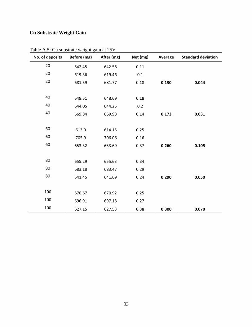
93
Cu Substrate Weight Gain Table A.5: Cu substrate weight gain at 25V No. of deposits Before (mg) After (mg) Net (mg) Average Standard deviation
20 642.45 642.56 0.11
20 619.36 619.46 0.1
20 681.59 681.77 0.18 0.130 0.044
40 648.51 648.69 0.18
40 644.05 644.25 0.2
40 669.84 669.98 0.14 0.173 0.031
60 613.9 614.15 0.25
60 705.9 706.06 0.16
60 653.32 653.69 0.37 0.260 0.105
80 655.29 655.63 0.34
80 683.18 683.47 0.29
80 641.45 641.69 0.24 0.290 0.050
100 670.67 670.92 0.25
100 696.91 697.18 0.27
100 627.15 627.53 0.38 0.300 0.070

94
Table A.6: Cu substrate weight gain at 35V No. of deposits Before (mg) After (mg) Net (mg) Average Standard deviation
20 423.38 423.58 0.2
20 438.02 438.12 0.1
20 432.08 432.21 0.13 0.143 0.051
40 422.1 422.23 0.13
40 439.48 439.56 0.08
40 445.25 445.48 0.23 0.147 0.076
60 437.3 437.58 0.28
60 440.46 440.61 0.15
60 425.73 425.94 0.21 0.213 0.065
80 831.06 831.24 0.18
80 905.19 905.53 0.34
80 876.5 876.86 0.36 0.293 0.099
100 977.59 977.74 0.15
100 899.45 899.77 0.32
100 962.46 962.86 0.4 0.290 0.128

95
Table A.7: Cu substrate weight gain at 45V No. of deposits Before (mg) After (mg) Net (mg) Average Standard deviation
20 679.39 679.52 0.13 20 633.96 634.18 0.22 20 662.71 662.94 0.23 0.193 0.055
40 617.08 617.53 0.45 40 694.17 694.31 0.14
40 699.37 699.72 0.35 0.313 0.158
60 662.63 663.16 0.53 60 706.85 707.26 0.41 60 696.45 696.89 0.44 0.460 0.062
80 669.22 670.13 0.91
80 677.13 677.73 0.6 80 684.39 685.28 0.89 0.800 0.173
100 673.42 674.24 0.82 100 676.48 677.45 0.97
100 664.61 665.51 0.9 0.897 0.075

96
Table A.8: Cu substrate weight gain at 65V No. of deposits Before (mg) After (mg) Net (mg) Average Standard deviation
20 700.98 701.15 0.17 20 628.57 628.63 0.06 20 653.93 654.32 0.39 0.207 0.168
40 666.71 667.02 0.31 40 676.86 677.06 0.2 40 659.5 659.84 0.34 0.283 0.074
60 712.8 713.26 0.46 60 668.3 668.73 0.43 60 712.31 712.9 0.59 0.493 0.085
80 718.7 719.35 0.65 80 698.13 698.72 0.59 80 642.02 642.69 0.67 0.637 0.042
100 653.43 654.18 0.75 100 667.6 668.76 1.16
100 668.98 669.72 0.74 0.883 0.240