Embed Size (px)
Citation preview

CONFIDENTIAL
Analog Reinvented
ES9016K2M Ultra 32-bit Stereo Low Power Audio DAC
Datasheet
ESS TECHNOLOGY, INC. 109 Bonaventura Drive, San Jose, CA 95134, USA Tel (408) 643-8800 • www.esstech.com
FEATURE DESCRIPTION
Patented 32-bit HyperStream® DAC o +122dB DNR o –110dB THD+N
o 32-bit audio DAC powered by Sabre32® DAC architecture with unmatched dynamic range and ultra low distortion
o Supports both synchronous and ASRC (asynchronous sample rate converter) modes
Patented Time Domain Jitter Eliminator o Unmatched audio clarity free from input clock jitter
64-bit accumulator and 32-bit processing o Distortion free signal processing
Integrated DSP Functions o Click-free soft mute and volume control o Programmable Zero detect o De-emphasis for 32kHz, 44.1kHz, and 48kHz sampling
Customizable output configuration o Mono or stereo output in current or voltage mode based on
performance criterion
I2C control o Allows software control of DAC features
28-QFN (5mm x 5mm) package o Minimizes PCB footprint
< 40mW operating, < 1mW standby power o Maximizes battery life
1.8 to 3.3V analog & digital power supplies o Reduces power and simplifies power supply design
1.8V digital logic supported o Connects to Application Processor without level shifter
Versatile digital input o Supports SPDIF, PCM (I2S, LJ 16-32-bit) or DSD input
Customizable filter characteristics o User programmable filter allowing custom roll-off response o Bypassable oversampling filter
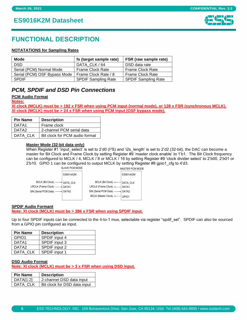
APPLICATIONS • Mobile phones / Tablets / Digital music players / Portable multimedia players
• Blu-ray / SACD / DVD-Audio player
• Audio preamplifier and A/V receiver
• Professional audio recording systems / Mixing consoles / Digital audio workstation
The ES9016K2M SABRE32® Ultra DAC is a high-performance 32-bit, 2-channel audio D/A converter targeted for portable high-fidelity audio power sensitive applications such as digital music players, consumer applications such as Blu-ray players, audio pre-amplifiers and A/V receivers, as well as professional applications such as recording systems, mixer consoles and digital audio workstations. Using the critically acclaimed ESS patented 32-bit HyperStream® DAC architecture and Time Domain Jitter Eliminator, the ES9016K2M SABRE32® Ultra DAC delivers a DNR of up to 122dB and THD+N of –110dB, a performance level that will satisfy the most demanding audio enthusiasts. The ES9016K2M SABRE32® Ultra DAC’s 32-bit HyperStream® architecture can handle up to 32-bit, 384kHz PCM data via I2S, DSD-11.2MHz data as well as mono mode for highest performance applications. Both synchronous and ASRC (asynchronous sample rate conversion) modes are supported. The ES9016K2M SABRE® Ultra DAC is powered by a +1.8V to +3.3V supply for both the digital and analog sections, with internal regulators generating the core supply. The DAC comes in a 28-QFN package, supports 1.8V logic levels and consumes less than 40mW in normal operating mode (< 1mW in standby mode) The SABRE® Ultra DAC sets a new standard for high quality audio performance, SABRE SOUND®, in a cost effective, easy-to-use form factor for today’s most demanding digital audio applications.
CONFIDENTIAL Rev. 3.2 March 26, 2021
ES9016K2M Datasheet
ESS TECHNOLOGY, INC. 109 Bonaventura Drive, San Jose, CA 95134, USA Tel (408) 643-8800 • www.esstech.com
2
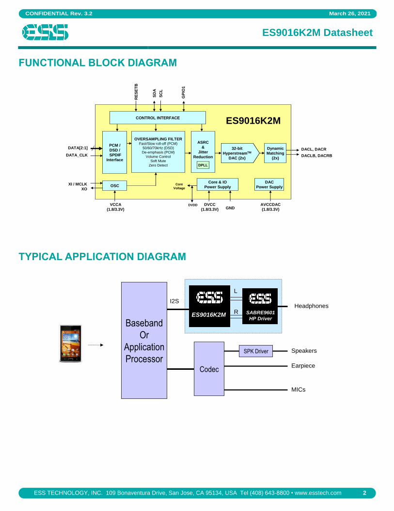
FUNCTIONAL BLOCK DIAGRAM
TYPICAL APPLICATION DIAGRAM
L
Baseband
Or
Application
Processor
ES9016K2MR
Headphones
Codec
I2S
Earpiece
MICs
SPK Driver Speakers
SABRE9601
HP Driver
ASRC
&
Jitter
Reduction
CONTROL INTERFACE
Core & IO
Power Supply
32-bit
HyperstreamTM
DAC (2x)
32-bit
HyperstreamTM
DAC (2x)
Dynamic
Matching
(2x)
DAC
Power Supply
DATA_CLK
RE
SE
TB
SD
A
SC
L
GND
XI / MCLK
XO
DPLL
DATA[2:1] DACL, DACR
DACLB, DACRB
ES9016K2M
AVCCDAC
(1.8/3.3V)
OSCG
PIO
1
PCM /
DSD /
SPDIF
Interface
OVERSAMPLING FILTERFast/Slow roll-off (PCM)
50/60/70kHz (DSD)
De-emphasis (PCM)
Volume Control
Soft Mute
Zero Detect
DVCC
(1.8/3.3V)
VCCA
(1.8/3.3V)
Core
Voltage
DVDD

March 26, 2021 CONFIDENTIAL Rev. 3.2
ES9016K2M Datasheet
3 ESS TECHNOLOGY, INC. 109 Bonaventura Drive, San Jose, CA 95134, USA Tel (408) 643-8800 • www.esstech.com
PIN LAYOUT
RE
SE
TB
DA
TA
_C
LK
DA
TA
1
DA
TA
2
GP
IO1
N.C
.
N.C
.
28
27
26
25
24
23
22
DGND 1 21 DVDD
N.C. 2 20 DGND
SCL 3 19 N.C.
SDA 4 18 DVCC
ADDR 5 17 VCCA
XO 6 16 AVCCDAC
XI (MCLK) 7 15 N.C.
8 9 10
11
12
13
14
N.C
.
DA
CR
DA
CR
B
N.C
.
AG
ND
DA
CL
DA
CL
BES9016K2M
28-QFN

CONFIDENTIAL Rev. 3.2 March 26, 2021
ES9016K2M Datasheet
ESS TECHNOLOGY, INC. 109 Bonaventura Drive, San Jose, CA 95134, USA Tel (408) 643-8800 • www.esstech.com
4
PIN DESCRIPTIONS
Pin Name Pin Type Reset State
Pin Description
1 DGND Ground Ground Digital Ground
2 N.C. - - No internal connection. Pin may be grounded if desired.
3 SCL I Tri-stated I2C Serial Clock Input
4 SDA I/O Tri-stated I2C Serial Data Input/Output
5 ADDR I Tri-stated I2C Address Select
6 XO AO Floating XTAL Out
7 XI (MCLK) AI Floating XTAL / MCLK In
8 N.C. - - No internal connection. Pin may be grounded if desired.
9 DACR AO Driven to ground
Differential Positive Analog Output Right
10 DACRB AO Driven to ground
Differential Negative Analog Output Right
11 N.C. - - No internal connection. Pin may be grounded if desired.
12 AGND Ground Ground Analog Ground
13 DACL AO Driven to ground
Differential Positive Analog Output Left
14 DACLB AO Driven to ground
Differential Negative Analog Output Left
15 N.C. - - No internal connection. Pin may be grounded if desired.
16 AVCCDAC Power Power Analog AVCC for DAC
17 VCCA Power Power Analog +1.8V or +3.3V for OSC
18 DVCC Power Power Digital +1.8V to +3.3V
19 N.C. - - No internal connection. Pin may be grounded if desired.
20 DGND Ground Ground Digital Ground
21 DVDD Power Power
Digital Core Voltage, nominally +1.2V, is supplied by a regulator from
DVCC. DVDD must be decoupled with a minimum 4.7F capacitor to DGND for stable operation. DVDD needs to be externally supplied for high XI / MCLK frequency. Please refer to the section about the DVDD supply on page 7 for additional information.
22 N.C. - - No internal connection. Pin may be grounded if desired.
23 N.C. - - No internal connection. Pin may be grounded if desired.
24 GPIO1 I/O Tri-stated GPIO 1
25 DATA2 I Tri-stated DSD Data2 (R) or PCM Data CH1/CH2 or SPDIF Input 2
26 DATA1 I/O Tri-stated Master mode off: Input for DSD Data1 (L) or PCM Frame Clock or SPDIF Input 3 Master mode on: Output for PCM Frame Clock
27 DATA_CLK I/O Tri-stated Master mode off: Input for PCM Bit Clock or DSD Bit Clock or SPDIF Input 1 Master mode on: Output for PCM Bit Clock
28 RESETB I Tri-stated Master Reset / Power Down (active low)
Exposed Pad
DGND Ground Ground Digital Ground. Connect the Exposed Pad to DGND
Notes: - There are 7 N.C. (No Connect) pins. If desired, these pins can be connected to ground on the PCB to strengthen the
otherwise isolated pin pads. - The exposed pad must be connected to digital ground.
March 26, 2021 CONFIDENTIAL Rev. 3.2
ES9016K2M Datasheet
5 ESS TECHNOLOGY, INC. 109 Bonaventura Drive, San Jose, CA 95134, USA Tel (408) 643-8800 • www.esstech.com
FUNCTIONAL DESCRIPTION
NOTATATIONS for Sampling Rates
Mode fs (target sample rate) FSR (raw sample rate)
DSD DATA_CLK / 64 DSD data rate
Serial (PCM) Normal Mode Frame Clock Rate Frame Clock Rate
Serial (PCM) OSF Bypass Mode Frame Clock Rate / 8 Frame Clock Rate
SPDIF SPDIF Sampling Rate SPDIF Sampling Rate
PCM, SPDIF and DSD Pin Connections PCM Audio Format Notes: XI clock (MCLK) must be > 192 x FSR when using PCM input (normal mode), or 128 x FSR (synchronous MCLK). XI clock (MCLK) must be > 24 x FSR when using PCM input (OSF bypass mode).
Pin Name Description
DATA1 Frame clock
DATA2 2-channel PCM serial data
DATA_CLK Bit clock for PCM audio format
Master Mode (32-bit data only) When Register #1 ‘input_select’ is set to 2’d0 (I2S) and ‘i2s_length’ is set to 2’d2 (32-bit), the DAC can become a master for Bit Clock and Frame Clock by setting Register #9 ‘master clock enable’ to 1’b1. The Bit Clock frequency can be configured to MCLK / 4, MCLK / 8 or MCLK / 16 by setting Register #9 ‘clock divider select’ to 2’b00, 2’b01 or 2’b10. GPIO 1 can be configured to output MCLK by setting Register #8 gpio1_cfg to 4’d3.
DATA_CLK
DATA1
DATA2SIN (Serial PCM Data)
ES901xK2M
DATA_CLK
DATA1
DATA2
ES901xK2M
GPIO1MCLK (Master Clock)
SLAVE PCM MODE MASTER PCM MODE
BCLK (Bit Clock)
LRCLK (Frame Clock)
BCLK (Bit Clock)
LRCLK (Frame Clock)
SIN (Serial PCM Data)
SPDIF Audio Formant Note: XI clock (MCLK) must be > 386 x FSR when using SPDIF input.
Up to four SPDIF inputs can be connected to the 4-to-1 mux, selectable via register “spdif_sel”. SPDIF can also be sourced from a GPIO pin configured as input.
Pin Name Description
GPIO1 SPDIF input 4
DATA1 SPDIF input 3
DATA2 SPDIF input 2
DATA_CLK SPDIF input 1
DSD Audio Format Note: XI clock (MCLK) must be > 3 x FSR when using DSD input.
Pin Name Description
DATA[1:2] 2-channel DSD data input
DATA_CLK Bit clock for DSD data input

CONFIDENTIAL Rev. 3.2 March 26, 2021
ES9016K2M Datasheet
ESS TECHNOLOGY, INC. 109 Bonaventura Drive, San Jose, CA 95134, USA Tel (408) 643-8800 • www.esstech.com
6
FEATURE DESCRIPTION
Soft Mute When Mute is asserted the output signal will ramp to the - level. When Mute is reset the attenuation level will ramp back up to the previous level set by the volume control register. Asserting Mute will not change the value of the volume control register. The ramp rate is 0.0078125 x fs / 2(vol_rate-5) dB/s.
Automute During an automute condition the ramping of the volume of each DAC to - can now be programmatically enabled or disabled. o In PCM serial mode, “AUTOMUTE” will become active once the audio data is continuously below the threshold set by
<Register Automute_lev>, for a length of time defined by 2096896 / (<Register#4> x 64 x fs) seconds. o In SPDIF mode, “AUTOMUTE” will become active once the audio data is continuously below the threshold set by
<Register Automute_lev>, for a length of time defined by 2096896 / (<Register#4> x (64 x fs) seconds. o In the DSD Mode, “AUTOMUTE” will become active when any 8 consecutive values in the DSD stream have as many 1’s
and 0’s for a length of time defined by 2096896 / (<Register Automute_time> x DATA_CLK) seconds. The following table summarizes the conditions.
Mode Detection Condition Time
PCM Data is continuously lower than <Register Automute_lev >
2096896 / (<Register Automute_time > x 64 x fs)
SPDIF Data is continuously lower than <Register Automute_lev >
2096896 / (<Register Automute_time > x (64 x fs))
DSD Equal number of 1s and 0s in every 8 bits of data
2096896 / (<Register Automute_time > x DATA_CLK)
Volume Control Each output channel has its own attenuation circuit. The attenuation for each channel is controlled independently. Each channel can be attenuated from 0dB to –127dB in 0.5dB steps. Each 0.5dB step transition takes up to 64 intermediate levels, depending on the vol_rate register setting. The result being that the level changes are done using small enough steps so that no switching noise occurs during the transition of the volume control. When a new volume level is set, the attenuation circuit will ramp softly to the new level.
Master Trim The master trim sets the 0dB reference level for the volume control of each DAC. The master trim is programmable via registers 17-20 and is a 32bit signed number. Therefore it should never exceed 32'h7FFFFFFF (as this is full-scale signed).
All Mono Mode An all mono mode where all DACs are driven from the same source is supported. This can be useful for high-end audio applications. The source data for all DACs can be programmatically configured to be either CH1 or CH2.
De-emphasis The de-emphasis feature is included for audio data that has utilized the 50/15s pre-emphasis for noise reduction. There are three de-emphasis filters, one for 32kHz, one for 44.1kHz, and one for 48kHz.
SPDIF Data Select An SPDIF source multiplexer allows for up to four SPDIF sources to be connected to the data pins. An internal programmable register (spdif_sel) is used to select the appropriate data or GPIO pin to decode. SPDIF can also be sourced from GPIO pin configured as input.

March 26, 2021 CONFIDENTIAL Rev. 3.2
ES9016K2M Datasheet
7 ESS TECHNOLOGY, INC. 109 Bonaventura Drive, San Jose, CA 95134, USA Tel (408) 643-8800 • www.esstech.com
System Clock (XI / MCLK) A system clock is required for proper operation of the digital filters and modulation circuitry. See p.28, Note 2 for the maximum MCLK frequencies supported. The minimum system clock frequency must also satisfy:
Data Type Minimum MCLK Frequency Note
DSD Data MCLK > 3 x FSR , FSR = 2.8224MHz (x 1, 2 or 4) The maximum FSR frequency is further limited by the maximum MCLK frequencies supported as shown p.28, Note 2.
Serial Normal Mode MCLK > 192 x FSR, FSR 384kHz or
MCLK = 128 x FSR (synchronous MCLK) with FSR 384kHz
Serial OSF Bypass Mode
MCLK > 24 x FSR, FSR 1.536MHz
SPDIF Data MCLK > 386 x FSR, FSR 200kHz
Data Clock DATA_CLOCK must be (2 x i2s_length) x FSR for SERIAL, and FSR for DSD modes. For SPDIF mode, this pin is used for SPDIF input. This pin should be pulled low if not used.
Built-in Digital Filters Three digital filters (fast roll-off, slow roll-off and minimum phase filters) are included for PCM data. See 'PCM Filter Characteristics' for more information.
Standby Mode For lowest power consumption, the following sequence should be performed to enter stand-by mode:
• Set the soft start bit in register 14 to 1'b0 to ramp the DAC outputs (DACL, DACLB, DACR, DACRB) to ground.
• RESETB pin should be brought to low digital level to: o Shut off the DACs, Oscillator and internal regulator. o Force digital I/O pins (DATA_CLK, DATA1, GPIO1, SDA ) into tri-state mode o Reset all registers to default states
• If XI/MCLK is supplied externally, it should be stopped at logic low level
• If DVDD is supplied by an external regulator, it should be shutdown during standby To resume from standby mode, bring RESETB to high digital level and reinitialize all registers.
DVDD Supply The ES9016K2M is equipped with an internal, regulated DVDD supply powered from DVCC. The internal DVDD regulator
must be decoupled to DGND with a 4.7F minimum capacitor for stable operation. Recommended capacitor for decoupling
DVDD is a 4.7F ±20%, X5R 6.3V 0402, e.g. TDK part number C1005X5R0J475M050BC or similar.
• The internal DVDD should be used except under the following conditions: 1. PCM (SPDIF, I2S with OSF Bypass off or on): MCLK > 50MHz or FSR > 192kHz 2. DSD: MCLK > 50MHz or FSR > 11.2MHz
• Internal DVDD may be used up to the maximum supported MCLK frequencies specified on p.28, Note 2. An External DVDD (+1.3V) supply must be used above those frequencies. The external supply voltage must be greater than the internal supply of +1.2V so the internal supply is disabled.

CONFIDENTIAL Rev. 3.2 March 26, 2021
ES9016K2M Datasheet
ESS TECHNOLOGY, INC. 109 Bonaventura Drive, San Jose, CA 95134, USA Tel (408) 643-8800 • www.esstech.com
8
Programmable FIR filter A two stage interpolating FIR design is used. The interpolating FIR filter is generated using MATLAB, and can then be downloaded using a custom C code. Example Source Code for Loading a Filter // only accept 128 or 16 coefficients // Note: The coefficients must be quantized to 24 bits for this method! // Note: Stage 1 consists of 128 values (0-127 being the coefficients) // Note: Stage 2 consists of 16 values (0-13 being the coefficients, 14-15 are zeros) // Note: Stage 2 is symmetric about coefficient 13. See the example filters for more information. byte reg26 = (byte)(coeffs.Count == 128 ? 0 : 128); for (int i = 0; i < coeffs.Count; i++) { // stage 1 contains 128 coefficients, while stage 2 contains 16 coefficients registers.WriteRegister(26, (byte)(reg26 + i)); // write the coefficient data registers.WriteRegister(27, (byte)(coeffs[i] & 0xff)); registers.WriteRegister(28, (byte)((coeffs[i] >> 8) & 0xff)); registers.WriteRegister(29, (byte)((coeffs[i] >> 16) & 0xff)); registers.WriteRegister(30, 0x02); // set the write enable bit } // disable the write enable bit when we're done registers.WriteRegister(30, (byte)(setEvenBit ? 0x04 : 0x00));
OSF Bypass The oversampling FIR filter can be bypassed, sourcing data directly into the IIR filter. ESS recommends using 8 x FSR as the input. For example, an external signal at 44.1kHz can be oversampled externally to 8 x 44.1kHz = 352.8kHz and then applied to the serial decoder in either I2S or LJ format. The maximum sample rate that can be applied is 1.536MHz (8 x 192kHz).

March 26, 2021 CONFIDENTIAL Rev. 3.2
ES9016K2M Datasheet
9 ESS TECHNOLOGY, INC. 109 Bonaventura Drive, San Jose, CA 95134, USA Tel (408) 643-8800 • www.esstech.com
Audio Interface Formats Several interface formats are provided so that direct connection to common audio processors is possible. The available formats and their accompanying diagrams are listed in the following table. The audio interface format can be set by programming the registers.
31 30 29 2 1 031 30 29 2 1 0 31 30 29 2 1 031 30 29 2 1 0SIN
32-bitMSB LSB MSB LSB MSB
31 30
BCLK
LRCLK LEFTRIGHT
LEFT JUSTIFIED FORMAT
31 30 29 2 1 031 30 29 2 1 0 31 30 29 2 1 031 30 29 2 1 0SIN
32-bitMSB LSB MSB LSB MSB
31 30
BCLK
LRCLK LEFTRIGHT
I2S FORMAT
23 22 21 2 1 023 22 21 2 1 0 23 22 21 2 1 023 22 21 2 1 0SIN
24-bitMSB LSB MSB LSB MSB
23 22
15 14 13 2 1 015 14 13 2 1 0 15 14 13 2 1 015 14 13 2 1 0SIN
16-bitMSB LSB MSB LSB MSB
15 14
23 22 21 2 1 023 22 21 2 1 0 23 22 21 2 1 023 22 21 2 1 0SIN
24-bitMSB LSB MSB LSB MSB
23 22
15 14 13 2 1 015 14 13 2 1 0 15 14 13 2 1 015 14 13 2 1 0SIN
16-bitMSB LSB MSB LSB MSB
15 14
Note: for Left-Justified and I2S formats, the following number of BCLKs is present per LRCLK frame (left plus right channels):
• 16-bit mode: 32 BCLKs
• 24-bit mode: 48 BCLKs
• 32-bit mode: 64 BCLKs
DCLK DSD1, DSD2 DCLK DSD1, DSD2
31 30 29 2 1 0 31 30 29 2 1 0
23 22 21 2 1 0 23 22 21 2 1 0
SIN
32-bitMSB LSB MSB LSB
MSB MSBLSB LSB
19 18 17 2 1 0 19 18 17 2 1 0
MSB MSBLSB LSB
15 14 13 2 1 0 15 14 13 2 1 0
MSB MSBLSB LSB
23 22
MSB
MSB
19 18
MSB
15 14
MSB
31 30
SIN
24-bit
SIN
20bit
SIN
16bit
BCLK
LRCLK LEFTRIGHT
FIGURE 1A
FIGURE 1A
FIGURE 1A
FIGURE 1A
LEFT JUSTIFIED FORMAT
31 30 29 2 1 031 30 29 2 1 0 31 30 29 2 1 031 30 29 2 1 0
23 22 21 2 1 0 23 22 21 2 1 0
SIN
32-bitMSB LSB MSB LSB
MSB MSBLSB LSB
19 18 17 2 1 0 19 18 17 2 1 0
MSB MSBLSB LSB
15 14 13 2 1 0 15 14 13 2 1 0
MSB MSBLSB LSB
MSB
31 30
SIN
24-bit
SIN
20bit
SIN
16bit
BCLK
LRCLK LEFTRIGHT
FIGURE 2A
FIGURE 2A
FIGURE 2A
FIGURE 2A
RIGHT JUSTIFIED FORMAT
31 30 29 2 1 031 30 29 2 1 0 31 30 29 2 1 031 30 29 2 1 0
23 22 21 2 1 0 23 22 21 2 1 0
SIN
32-bitMSB LSB MSB LSB
MSB MSBLSB LSB
19 18 17 2 1 0 19 18 17 2 1 0
MSB MSBLSB LSB
15 14 13 2 1 0 15 14 13 2 1 0
MSB MSBLSB LSB
23 22
MSB
MSB
19 18
MSB
15 14
MSB
31 30
SIN
24-bit
SIN
20bit
SIN
16bit
BCLK
LRCLK LEFTRIGHT
FIGURE 3A
FIGURE 3A
FIGURE 3A
FIGURE 3A
I2S FORMAT
D.. D0 D1 D2 D3 D4D1
D2
DCLK
FIGURE 4A
D.. D0 D1 D2 D3 D4D1
D2
DCLK
FIGURE 4BD.. D0 D1 D2 D3 D4
DSD NORMAL MODE
DSD PHASE MODE
CONFIDENTIAL Rev. 3.2 March 26, 2021
ES9016K2M Datasheet
ESS TECHNOLOGY, INC. 109 Bonaventura Drive, San Jose, CA 95134, USA Tel (408) 643-8800 • www.esstech.com
10
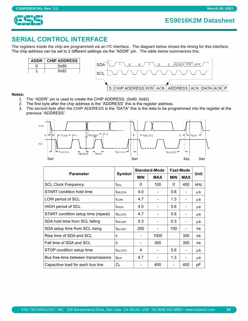
SERIAL CONTROL INTERFACE The registers inside the chip are programmed via an I2C interface. The diagram below shows the timing for this interface. The chip address can be set to 2 different settings via the “ADDR” pin. The table below summarizes this.
ADDR CHIP ADDRESS
0 0x90
1 0x92
Notes:
1. The “ADDR” pin is used to create the CHIP ADDRESS. (0x90, 0x92) 2. The first byte after the chip address is the “ADDRESS” this is the register address. 3. The second byte after the CHIP ADDRESS is the “DATA” this is the data to be programmed into the register at the
previous “ADDRESS”.
Start Start StartStop
Parameter Symbol Standard-Mode Fast-Mode
Unit MIN MAX MIN MAX
SCL Clock Frequency fSCL 0 100 0 400 kHz
START condition hold time tHD,STA 4.0 - 0.6 - s
LOW period of SCL tLOW 4.7 - 1.3 - s
HIGH period of SCL tHIGH 4.0 - 0.6 - s
START condition setup time (repeat) tSU,STA 4.7 - 0.6 - s
SDA hold time from SCL falling tHD,DAT 0.3 - 0.3 - s
SDA setup time from SCL rising tSU,DAT 250 - 100 - ns
Rise time of SDA and SCL tr - 1000 300 ns
Fall time of SDA and SCL tf - 300 300 ns
STOP condition setup time tSU,STO 4 - 0.6 - s
Bus free-time between transmissions tBUF 4.7 - 1.3 - s
Capacitive load for each bus line Cb - 400 - 400 pF

March 26, 2021 CONFIDENTIAL Rev. 3.2
ES9016K2M Datasheet
11 ESS TECHNOLOGY, INC. 109 Bonaventura Drive, San Jose, CA 95134, USA Tel (408) 643-8800 • www.esstech.com
REGISTER MAP
Address (Dec/Hex)
Register D7 (MSB) D6 D5 D4 D3 D2 D1 D0 (LSB)
Read/Write 0 / 0x00 SYSTEM SETTINGS OSC_DRV RESERVED SOFT_RESET
1 / 0x01 INPUT
CONFIGURATION I2S_LENGTH I2S_MODE AUTO_INPUT_SELECT INPUT_SELECT
2 / 0x02 RESERVED RESERVED
3 / 0x03 RESERVED RESERVED
4 / 0x04 AUTOMUTE _TIME AUTOMUTE_TIME
5 / 0x05 AUTOMUTE
_LEVEL AUTOMUTE_ LOOPBACK
AUTOMUTE_LEVEL
6 / 0x06 SOFT VOLUME CONTROL 3 & DE-EMPHASIS
SPDIF_AUTO _DEEMPH
DEEMPH _BYPASS
DEEMPH_SEL RESERVED VOL_RATE
7 / 0x07 GENERAL SETTINGS
RESERVED FILTER_SHAPE RESERVED IIR_WR MUTE
8 / 0x08 GPIO
CONFIGURATION RESERVED GPIO1_CFG
9 / 0x09 RESERVED RESERVED FOR REVISION V
10 / 0x0A MASTER MODE
CONTROL MASTER_CLK
_ENABLE CLOCK_DIVIDER_SELECT
SYNC_ MODE
STOP_DIV
11 / 0x0B CHANNEL MAPPING
RESERVED SPDIF_SEL CH2_ANALOG
_SWAP CH1_ANALOG
_SWAP CH2_SEL CH1_SEL
12 / 0x0C DPLL/ASRC SETTINGS
DPLL_BW_I2S DPLL_BW_DSD
13 / 0x0D THD
COMPENSATION RESERVED BYPASS_THD RESERVED
14 / 0x0E SOFT START
SETTINGS SOFT_START
SOFT_START_ON_LOCK
MUTE_ON _LOCK
SOFT_START_TIME
15 / 0x0F VOLUME 1 VOLUME 1
16 / 0x10 VOLUME 2 VOLUME 2
17 / 0x11
MASTER TRIM MASTER_TRIM 18 / 0x12
19 / 0x13
20 / 0x14
21 / 0x15 GPIO INPUT
SELECTION & OSF BYPASS
GPIO_INPUT_SEL2 GPIO_INPUT_SEL1 RESERVED BYPASS_IIR RESERVED BYPASS_OSF
22 / 0x16 2ND HARMONIC COMPENSATION COEFFICIENTS
THD_COMP_C2 23 / 0x17
24 / 0x18 3RD HARMONIC COMPENSATION COEFFICIENTS
THD_COMP_C3 25 / 0x19
26 / 0x1A PROGRAMMABLE FILTER ADDRESS
PROG_COEFF_STAGE
PROG_COEFF_ADDR
27 / 0x1B PROGRAMMABLE FILTER
COEFFICIENT PROG_COEFF 28 / 0x1C
29 / 0x1D
30 / 0x1E PROGRAMMABLE FILTER CONTROL
RESERVED EVEN_STAGE2
_COEFF PROG_
COEFF_WE PROG_
COEFF_EN
Read Only
64 / 0x40 CHIP STATUS RESERVED REVISION CHIP_ID AUTOMUTE
_STATUS LOCK_STATUS
65 / 0x41 GPIO STATUS RESERVED GPIO_I[0]
66 / 0x42
DPLL RATIO DPLL_NUM 67 / 0x43
68 / 0x44
69 / 0x45
70-93 / 0x46-0x5D
CHANNEL STATUS SPDIF CHANNEL STATUS

CONFIDENTIAL Rev. 3.2 March 26, 2021
ES9016K2M Datasheet
ESS TECHNOLOGY, INC. 109 Bonaventura Drive, San Jose, CA 95134, USA Tel (408) 643-8800 • www.esstech.com
12
REGISTER SETTINGS
Register #0: System Settings 8 bit, Read-Write Register, Default = 0x00
Bits [7] [6] [5] [4] [3] [2] [1] [0]
Mnemonic osc_drv reserved * soft_reset
Default 0 0 0 0 0 0 0 0
Bit Mnemonic Description
[7:4] osc_drv
Oscillator drive specifies the bias current to the oscillator pad.
• 4'b0000: full bias (default)
• 4'b1000: 3/4 bias
• 4'b1100: 1/2 bias
• 4'b1110: 1/4 bias
• 4'b1111: shut down the oscillator
• Other settings: reserved It is recommended to use the default setting.
[3:1] reserved *
[0] soft_reset 1'b0 is normal operation (default) 1'b1 resets chip
* All Reserved Bits in Register #0 must be set to the indicated logic level to ensure correct device operation.
Register #1: Input Configuration 8 bit, Read-Write Register, Default = 0x8C
Bits [7] [6] [5] [4] [3] [2] [1] [0]
Mnemonic i2s_length i2s_mode auto_input_select input_select
Default 1 0 0 0 1 1 0 0
Bit Mnemonic Description
[7:6] i2s_length 2'd0 = 16bit 2'd1 = 24bit 2'd2 or 2'd3 = 32bit (default)
[5:4] i2s_mode
2’d0 = I2S (default) 2’d1 = LJ mode 2’d2 = I2S 2’d3 = LJ mode
[3:2] auto_input_select
2'd0 = 'input select', 2'd1 = I2S or DSD, 2'd2 = I2S or SPDIF, 2'd3 = I2S, SPDIF or DSD (default)
[1:0] input_select
2'd0 = I2S (default) 2'd1 = SPDIF 2'd2 = reserved 2'd3 = DSD

March 26, 2021 CONFIDENTIAL Rev. 3.2
ES9016K2M Datasheet
13 ESS TECHNOLOGY, INC. 109 Bonaventura Drive, San Jose, CA 95134, USA Tel (408) 643-8800 • www.esstech.com
Register #2: Reserved 8 bit, Read-Write Register, Default = 0x18
Bits [7] [6] [5] [4] [3] [2] [1] [0]
Mnemonic Reserved
Default 0 0 0 1 1 0 0 0
Register #3: Reserved 8 bit, Read-Write Register, Default = 0x10
Bits [7] [6] [5] [4] [3] [2] [1] [0]
Mnemonic Reserved
Default 0 0 0 1 0 0 0 0
Register #4: Soft Volume Control 1 (Automute Time) 8 bit, Read-Write Register, Default = 0x00
Bits [7] [6] [5] [4] [3] [2] [1] [0]
Mnemonic automute_time
Default 0 0 0 0 0 0 0 0
Bit Mnemonic Description
[7:0] automute_time Default of 8'd0 (Automute Disabled) Time in Seconds = 2096896 / (automute_time x DATA_CLK) with DATA_CLK in Hz
Register #5: Soft Volume Control 2 (Automute Level) 8 bit, Read-Write Register, Default = 0x68
Bits [7] [6] [5] [4] [3] [2] [1] [0]
Mnemonic automute_loopback automute_level
Default 0 1 1 0 1 0 0 0
Bit Mnemonic Description
[7] automute_loopback 1'b0 disables automute_loopback (default) 1'b1 ramps to -infinity on automute
[6:0] automute_level The level (in 1dB increments) of the automute, default of 7'd104

CONFIDENTIAL Rev. 3.2 March 26, 2021
ES9016K2M Datasheet
ESS TECHNOLOGY, INC. 109 Bonaventura Drive, San Jose, CA 95134, USA Tel (408) 643-8800 • www.esstech.com
14
Register #6: Soft Volume Control 3 and De-emphasis 8 bit, Read-Write Register, Default = 0x4A
Bits [7] [6] [5] [4] [3] [2] [1] [0]
Mnemonic spdif_auto_deemph deemph_bypass deemph_sel reserved * vol_rate
Default 0 1 0 0 1 0 1 0
Bit Mnemonic Description
[7] spdif_auto_deemph 1'b0 disables automatic de-emphasis select in SPDIF mode (default) 1'b1 enables automatic de-emphasis select in SPDIF mode
[6] deemph_bypass 1'b0 enables de-emphasis filters 1'b1 disabled de-emphasis filters (default)
[5:4] deemph_sel
2’b00 = 32kHz (default) 2’b01 = 44.1kHz 2’b10 = 48kHz 2’b11 = RESERVED
[3] reserved * Must be left as 1'b1 for normal operation
[2:0] vol_rate 3'd2 by default Sets the volume ramp rate to 0.0078125 x fs / 2(vol_rate-5) dB/s
* All Reserved Bits in Register #6 must be set to the indicated logic level to ensure correct device operation.
Register #7: General Settings 8 bit, Read-Write Register, Default = 0x80
Bits [7] [6] [5] [4] [3] [2] [1] [0]
Mnemonic reserved filter_shape reserved * iir_bw mute
Default 1 0 0 0 0 0 0 0
Bit Mnemonic Description
[7] reserved *
[6:5] filter_shape
2'd0 = fast rolloff (default) 2'd1 = slow rolloff 2'd2 = minimum phase 2'd3 = reserved
[4] reserved
[3:2] iir_bw
2'd0 = 1.0757 x fs or 47.44kHz (fs = 44.1kHz) - Normal mode (default) 2'd1 = 1.1338 x fs or 50kHz (fs = 44.1kHz) 2'd2 = 1.3605 x fs or 60kHz (fs = 44.1kHz) 2'd3 = 1.5873 x fs or 70kHz (fs = 44.1kHz)
[1:0] mute
This is a soft mute, which uses the ramping volume control. mute[0]
• 1’b0: Channel 1 (default of left channel) unmuted (default)
• 1’b1: Channel 1 (default of left channel) muted mute[1]
• 1’b0: Channel 2 (default of right channel) unmuted (default)
• 1’b1: Channel 2 (default of right channel) muted
* All Reserved Bits in Register #7 must be set to the indicated logic level to ensure correct device operation.

March 26, 2021 CONFIDENTIAL Rev. 3.2
ES9016K2M Datasheet
15 ESS TECHNOLOGY, INC. 109 Bonaventura Drive, San Jose, CA 95134, USA Tel (408) 643-8800 • www.esstech.com
Register #8: GPIO Configuration 8 bit, Read-Write Register, Default = 0x10
Bits [7] [6] [5] [4] [3] [2] [1] [0]
Mnemonic reserved gpio1_cfg
Default 0 0 0 1 0 0 0 0
Bit Mnemonic Description
[7:4] reserved
[3:0] gpio1_cfg Set GPIO 1 configuration Default to 4’d0 (Automute Status). See GPIO Configuration Table below for meaning of all settings.
GPIO Configuration Table
Setting Direction GPIO Function
4'd0 Output Automute status (active high) – asserted when Automute condition is met
4'd1 Output DPLL Lock status (active high) – asserted when DPLL is in lock
4'd2 Output Minimum Volume (active high) - asserted when volume of both the left and right channels has ramped to its
minimum value (–127.5dB).
4'd3 Output MCLK
4'd4 Output DPLL Lock interrupt (active high) - asserted when DPLL Lock status changes state - reading register 64 clears the interrupt
4'd5 Output Automute Interrupt (active high) - asserted when Automute status changes state - reading register 64 clears the interrupt
4'd6 Output DPLL Lock or Automute interrupt (active high) - asserted when DPLL Lock or Automute status changes state - reading register 64 clears the interrupt
4'd7 Output Output low
4'd8 Input Use as input pin - pin status can be read from register 65.
4'd9 Input Input Selection - uses the GPIO as an input select based on register 21
4'd15 Output Output high
Register #9: Reserved 8 bit, Read-Write Register, Default = 0x22
Bits [7] [6] [5] [4] [3] [2] [1] [0]
Mnemonic Reserved for Revision V
Default 0 0 0 0 0 0 0 0

CONFIDENTIAL Rev. 3.2 March 26, 2021
ES9016K2M Datasheet
ESS TECHNOLOGY, INC. 109 Bonaventura Drive, San Jose, CA 95134, USA Tel (408) 643-8800 • www.esstech.com
16
Register #10: Master Mode Control 8 bit, Read-Write Register, Default = 0x5
Bits [7] [6] [5] [4] [3] [2] [1] [0]
Mnemonic master_clock_enable clock_divider_select sync_mode stop_div
Default 0 0 0 0 0 1 0 1
Bit Mnemonic Description
[7] master_clock_enable 1'b0 disables master mode (default) 1'b1 enables master mode (driving Bit clock and Frame Clock)
[6:5] clock_divider_select
2'b00: Bit Clock frequency = MCLK / 4 (default) 2'b01: Bit Clock frequency = MCLK / 8 2b10: Bit Clock frequency = MCLK / 16 2'b11: Bit Clock frequency = MCLK / 16 Frame Clock frequency = Bit Clock frequency / 64
[4] sync_mode
1'b1 to enable quick lock if the fs and MCLK are synchronous and MCLK is 128 x FSR. 1'b0 for normal operation of the DPLL and ASRC. Note: quick lock can only be used in PCM normal mode.
[3:0] stop_div
Sets the number of FSR edges that must occur before the DPLL and ASRC can lock on to the incoming signal. 4'd0 = 16384 FSR edges 4'd1 = 8192 FSR edges 4'd2 = 5461 FSR edges 4'd3 = 4096 FSR edges 4'd4 = 3276 FSR edges 4'd5 = 2730 FSR edges (default) 4'd6 = 2340 FSR edges 4'd7 = 2048 FSR edges 4'd8 = 1820 FSR edges 4'd9 = 1638 FSR edges 4'd10 = 1489 FSR edges 4'd11 = 1365 FSR edges 4'd12 = 1260 FSR edges 4'd13 = 1170 FSR edges 4'd14 = 1092 FSR edges 4'd15 = 1024 FSR edges
For correct operation, master mode should only be enabled when the DAC’s input mode is set to I2S, and when i2s_length is set to 32-bit and i2s_mode is set to I2S in register 1. When master mode is enabled, the DATA_CLK pin will output Bit Clock and the DATA1 pin will output Frame Clock at frequencies specified by clock divider select. For compatibility with Rev. W, or when PCM data with FSR > 96kHz is used, stop_div should be set to 4’d0 (16384 FSR edges).

March 26, 2021 CONFIDENTIAL Rev. 3.2
ES9016K2M Datasheet
17 ESS TECHNOLOGY, INC. 109 Bonaventura Drive, San Jose, CA 95134, USA Tel (408) 643-8800 • www.esstech.com
Register #11: Channel Mapping 8 bit, Read-Write Register, Default = 0x02
Bits [7] [6] [5] [4] [3] [2] [1] [0]
Mnemonic reserved * spdif_sel ch2_analog_swap ch1_analog_swap ch2_sel ch1_sel
Default 0 0 0 0 0 0 1 0
Bit Mnemonic Description
[7] reserved *
[6:4] spdif_sel
select the spdif data source 3’d0 = DATA_CLK (default) 3’d1 = DATA2 3’d2 = DATA1 3’d3 = GPIO1 3’d4-7: reserved
[3] ch2_analog_swap 1'b0 = normal operation (default) 1'b1 = swap dac and dacb
[2] ch1_analog_swap 1'b0 = normal operation (default) 1'b1 = swap dac and dacb
[1] ch2_sel 1'b0 = left 1'b1 = right (default)
[0] ch1_sel 1'b0 = left (default) 1'b1 = right
* All Reserved Bits in Register #11 must be set to the indicated logic level to ensure correct device operation. Left and Right channels can be reversed using Register #11.

CONFIDENTIAL Rev. 3.2 March 26, 2021
ES9016K2M Datasheet
ESS TECHNOLOGY, INC. 109 Bonaventura Drive, San Jose, CA 95134, USA Tel (408) 643-8800 • www.esstech.com
18
Register #12: DPLL/ASRC Settings 8 bit, Read-Write Register, Default = 0x5A
Bits [7] [6] [5] [4] [3] [2] [1] [0]
Mnemonic dpll_bw_i2s dpll_bw_dsd
Default 0 1 0 1 1 0 1 0
Bit Mnemonic Description
[7:4] dpll_bw_i2s
DPLL bandwidth setting for I2S and SPDIF modes (16 settings) 4’b0000 : OFF 4’b0001 : Lowest Bandwidth 4’b0101 : (default) 4’b1010 : 4’b1111 : Highest Bandwidth
[3:0] dpll_bw_dsd
DPLL bandwidth setting for DSD mode (16 settings) 4’b0000 : OFF 4’b0001 : Lowest Bandwidth 4’b0101 : 4’b1010 : (default) 4’b1111 : Highest Bandwidth
Register #13: THD Compensation 8 bit, Read-Write Register, Default = 0x40
Bits [7] [6] [5] [4] [3] [2] [1] [0]
Mnemonic reserved * bypass_thd reserved *
Default 0 1 0 0 0 0 0 0
Bit Mnemonic Description
[7] reserved *
[6] bypass_thd
1’b0: enable THD compensation
• output = input + (input2) x thd_comp_c2 + (input3) x thd_comp_c3
• thd_comp_c2 is stored in registers 23-22 (16 bits signed) (register 23 stores MSBs)
• thd_comp_c3 is stored in registers 25-24 (16 bits signed) (register 25 stores MSBs) 1’b1: disable THD compensation (default)
• PCM mode: output = input; DSD mode: output = input / 2
[5:0] reserved
* All Reserved Bits in Register #13 must be set to the indicated logic level to ensure correct device operation. THD compensation can be used to reduce the 2nd and 3rd harmonic distortion introduced by external output drivers. A system level tuning is required to arrive at the optimum coefficients for thd_comp_c2 and thd_comp_c3. Notes:
• To get the same gain (output = input) for PCM and DSD modes without THD compensation, bypass_thd should be set to 1’b0 with thd_comp_c2 and thd_comp_c3 set to 16’d0 (default)
• Erroneous compensation can lead to higher distortion than the one without compensation. If accurate tuning cannot be performed, thd_comp_c2 and thd_comp_c3 should be set to 16’d0 (default) if bypass_thd is set to 1’b0.

March 26, 2021 CONFIDENTIAL Rev. 3.2
ES9016K2M Datasheet
19 ESS TECHNOLOGY, INC. 109 Bonaventura Drive, San Jose, CA 95134, USA Tel (408) 643-8800 • www.esstech.com
Register #14: Soft Start Settings 8 bit, Read-Write Register, Default = 0x8A
Bits [7] [6] [5] [4] [3] [2] [1] [0]
Mnemonic soft_start soft_start_on_lock mute_on_lock soft_start_time
Default 1 0 0 0 1 0 1 0
Bit Mnemonic Description
[7] soft_start 1'b0: Ramp the output stream to ground 1'b1: Normal operation (default) - ramp the output stream to ½ x AVCC_L/R
[6] soft_start_on_lock 1'b0: Do not force output low when lock is lost (default) 1’b1: Force output low when lock is lost
[5] mute_on_lock 1’b0: Do not force a mute when lock is lost (default) 1’b1: Force a mute when lock is lost
[4:0] soft_start_time
Time for soft start ramp = 4096 x 2(soft_start_time+1) / MCLK seconds (where MCLK is measured in Hz). The valid range of soft-start_time is from 0 to 20.
Register #15: Volume 1 (usually selected for the Left Channel, but can be reversed using Register #11)
8 bit, Read-Write Register, Default = 0x00
Bits [7] [6] [5] [4] [3] [2] [1] [0]
Mnemonic volume1
Default 0 0 0 0 0 0 0 0
Bit Mnemonic Description
[7:0] volume1 Default to 8'd0 0dB to –127.5dB in 0.5dB steps
Register #16: Volume 2 (usually selected for the Right Channel, but can be reversed using Register #11)
8 bit, Read-Write Register, Default = 0x00
Bits [7] [6] [5] [4] [3] [2] [1] [0]
Mnemonic volume2
Default 0 0 0 0 0 0 0 0
Bit Mnemonic Description
[7:0] volume2 Default to 8'd0 0dB to –127.5dB in 0.5dB steps
Register #20-17: Master Trim 32 bit, Read-Write Register, Default = 32’h7ffffff. Reg 20 are the MSB’s, Reg 17 are the LSB’s.
Bits [31:0]
Mnemonic master_trim
Default 32'h7fffffff
This is a 32 bit value that sets the 0dB level for all volume controls. This is a signed number, so it should never exceed 32'h7fffffff (which is 231 - 1).

CONFIDENTIAL Rev. 3.2 March 26, 2021
ES9016K2M Datasheet
ESS TECHNOLOGY, INC. 109 Bonaventura Drive, San Jose, CA 95134, USA Tel (408) 643-8800 • www.esstech.com
20
Register #21: GPIO Input Selection and OSF Bypass 8 bit, Read-Write Register, Default = 0x00
Bits [7:6] [5:4] [3] [2] [1] [0]
Mnemonic gpio_input_sel2 gpio_input_sel1 reserved * bypass_iir reserved * bypass_osf
Default 0 0 0 0 0 0 0 0
Bit Mnemonic Description
[7:6] gpio_input_sel2
Selects which input will be selected when GPIOX = 1'b1 2'd0 = I2S data (default) 2'd1 = SPDIF data 2’d2 = reserved 2'd3 = DSD data
[5:4] gpio_input_sel1
Selects which input will be selected when GPIOX = 1'b0 2'd0 = I2S data (default) 2'd1 = SPDIF data 2’d2 = reserved 2'd3 = DSD data
[3] reserved *
[2] bypass_iir 1'b0 = Use the IIR filter (default) 1'b1 = Bypass the IIR filter.
[3] reserved *
[0] bypass_osf
1'b0 = Use the interpolating 8x FIR filter (default) 1'b1 = Bypass the interpolating 8x FIR filter. Note: Bypassing the interpolating filter requires that the input data be oversampled at 8x fs by an external oversampling filter.
* All Reserved Bits in Register #21 must be set to the indicated logic level to ensure correct device operation. Note: Any of the GPIO can be configured to be used as an input select. This allows an external MCU or controller to set the input type by setting the GPIO to either logic high (1'b1) or logic low (1'b0). To set this feature, the first step is to enable one of the GPIO as an input select by setting gpio_cfg to 4'd9. Once a GPIO is configured as an input select it has the ability to select between two different inputs. The first input (logic low) is set via register 21[5:4]. The second input (logic high) is set via register 21[7:6].
Register #23-22: 2nd Harmonic Compensation Coefficients 16 bit, Read-Write Register, Default = 0x0000 (no compensation). Register #23 is MSB. See Register #13 for more details.
Bits [15:0]
Mnemonic Thd_comp_c2
Default 16’d0
Register #25-24: 3rd Harmonic Compensation Coefficients 16 bit, Read-Write Register, Default = 0x0000 (no compensation). Register #25 is MSB. See Register #13 for more details.
Bits [15:0]
Mnemonic Thd_comp_c3
Default 16’d0

March 26, 2021 CONFIDENTIAL Rev. 3.2
ES9016K2M Datasheet
21 ESS TECHNOLOGY, INC. 109 Bonaventura Drive, San Jose, CA 95134, USA Tel (408) 643-8800 • www.esstech.com
Register #26: Programmable Filter Address 8 bit, Read-Write Register, Default = 0x00
Bits [7] [6:0]
Mnemonic prog_coeff_stage prog_coeff_addr
Default 0 0 0 0 0 0 0 0
Bit Mnemonic Description
[7] prog_coeff_stage Selects which stage of the filter to write. 1'b0 = Stage 1 of the oversampling filter (128 coefficients) 1'b1 = Stage 2 of the oversampling filter (16 coefficients)
[6:0] prog_coeff_addr Selects the coefficient address when writing custom coefficients for the oversampling filter.
Register #29-27: Programmable Filter Coefficient 8 bit, Read-Write Register, Default = 0x000000
Bits [23:0]
Mnemonic prog_coeff
Default 24’d0
Bit Mnemonic Description
[23:0] prog_coeff A 24bit filter coefficients that will be written to address 'prog_coeff_addr'.
Register #30: Programmable Filter Control 8 bit, Read-Write Register, Default = 0x00
Bits [7:3] [2] [1] [0]
Mnemonic reserved * even_stage2_coeff prog_coeff_we prog_coeff_en
Default 0 0 0 0 0 0 0 0
Bit Mnemonic Description
[7:3] reserved *
[2] even_stage2_coeff Sets the type of symmetry of the stage 2 programmable filter. 1'b0 = Uses a sine symmetric filter (27 coefficients). 1'b1 = Uses a cosine symmetric filter (28 coefficients).
[1] prog_coeff_we
1'b0 = Disable writing to the custom filter coefficients. 1'b1 = Enable writing to the custom filter coefficients. Note: When set to 1'b1 the custom filter will be bypassed regardless of the state of register 21[0].
[0] prog_coeff_en
1'b0 = Use one of the built-in oversampling filters. 1'b1 = Use the custom oversampling filter. Note: The custom filter is not programmed to anything on reset, valid coefficients must be written to the filter before enabling.
* All Reserved Bits in Register #30 must be set to the indicated logic level to ensure correct device operation. Note: even_stage2_coeff sets the type of symmetry used by the second stage filter. The actual RAM is 16 coefficients, but only the first 14 coefficients are used when applying the oversampling filter. The first 14 coefficients are mirrored using either sine or cosine symmetry, resulting in a filter length of either 27 or 28 taps. This means that the second stage RAM should only contain half of the impulse response of the second stage filter, and the impulse peak value will be contained in the 14th coefficient. Also note that, due to the symmetry of the filter, only linear phase filters may be used in the second stage.

CONFIDENTIAL Rev. 3.2 March 26, 2021
ES9016K2M Datasheet
ESS TECHNOLOGY, INC. 109 Bonaventura Drive, San Jose, CA 95134, USA Tel (408) 643-8800 • www.esstech.com
22
Register #64: Chip Status 8 bit, Read-Only Register
Bits [7] [6] [5] [4] [3] [2] [1] [0]
Mnemonic Reserved revision chip_id automute_status lock_status
Bit Mnemonic Description
[7:6] Reserved
[5] revision 1'b0 => revision W. 1'b1 => revision V.
[4:2] chip_id 3’d6 => ES9016K2M
[1] automute_status 1'b0 => Automute condition is inactive. 1'b1 => Automute condition is active.
[0] lock_status 1'b0 => The Jitter Eliminator is not locked to an incoming signal. 1'b1 => The Jitter Eliminator is locked to an incoming signal.
Register #65 8 bit, Read-Only Register
Bits [7] [6] [5] [4] [3] [2] [1] [0]
Mnemonic reserved gpio_I[1:0]
Bit Mnemonic Description
[7:2] reserved
[0] gpio_I[0] Status of pin GPIO1
Register #69-66: DPLL Ratio 32 bit, Read-Only Register. Reg 69 are the MSB’s, Reg 66 are the LSB’s
Bits [31:0]
Mnemonic dpll_num
This is a read-only 32bit value that can be used to calculate the sample rate. The raw sample rate (FSR) can be calculated using: FSR = (DPLL_NUM x FMCLK) / 232. Note that the DPLL number (register 66-69) should be read from LSB to MSB as it is latched on the LSBs (register 66).
Register #93-70: Channel Status Reg 93 are the MSB’s, Reg 70 are the LSB’s Format is [191:0] These registers allow read back of the SPDIF channel status. The status definition is different for the consumer configuration and professional configuration. Please refer to the following two tables for details.

March 26, 2021 CONFIDENTIAL Rev. 3.2
ES9016K2M Datasheet
23 ESS TECHNOLOGY, INC. 109 Bonaventura Drive, San Jose, CA 95134, USA Tel (408) 643-8800 • www.esstech.com
SPDIF CHANNEL STATUS - Consumer configuration Address Offset
[7] [6] [5] [4] [3] [2] [1] [0]
0 Reserved Reserved 0:2Channel 1:4Channel
Reserved 0:No-Preemph 1:Preemph
0:CopyRight 1:Non-CopyRight
0:Audio 1:Data
0:Consumer 1:Professional
1 Category Code 0x00: General 0x01: Laser-Optical 0x02: D/D Converter 0x03: Magnetic 0x04: Digital Broadcast 0x05: Musical Instrument 0x06: Present A/D Converter 0x08: Solid State Memory 0x16: Future A/D Converter 0x19: DVD 0x40: Experimental
2 Channel Number 0x0: Don't Care 0x1: A (Left) 0x2: B (Right) 0x3: C 0x4: D 0x5: E 0x6: F 0x7: G 0x8: H 0x9: I 0xA: J 0xB: K 0xC: L 0xD: M 0xE: N 0xF: O
Source Number 0x0: Don't Care 0x1: 1 0x2: 2 0x3: 3 0x4: 4 0x5: 5 0x6: 6 0x7: G 0x8: 8 0x9: 9 0xA: 10 0xB: 11 0xC: 12 0xD: 13 0xE: 14 0xF: 15
3 Reserved Reserved Clock Accuracy 0x0:Level 2 +-1000ppm 0x1:Level 1 +-50ppm 0x2:Level 3 variable pitch shifted
Sample Frequency 0x0: 44.1k 0x2: 48k 0x3: 32k 0x4: 22.05k 0x6: 24k 0x8: 88.2k 0xA: 96k 0xC: 176.4k 0xE: 192k
4 Reserved Reserved Reserved Reserved Word Length: If Word Field Size=0 |If Word Field Size = 1 000=Not indicated |000=Not indicated 100 = 23bits |100 = 19bits 010 = 22bits |010 = 18bits 110 = 21bits |110 = 17bits 001 = 20bits |001 = 16bits 101 = 24bits |101 = 20bits
Word Field Size 0:Max 20bits 1:Max 24bits
5-23 Reserved

CONFIDENTIAL Rev. 3.2 March 26, 2021
ES9016K2M Datasheet
ESS TECHNOLOGY, INC. 109 Bonaventura Drive, San Jose, CA 95134, USA Tel (408) 643-8800 • www.esstech.com
24
SPDIF CHANNEL STATUS - Professional configuration Address Offset
[7] [6] [5] [4] [3] [2] [1] [0]
0 sampling frequency: 00: not indicated (or see byte 4) 10: 48kHz 01: 44.1kHz 11: 32kHz
lock: 0: locked 1: unlocked
emphasis: 000: Emphasis not indicated 001: No emphasis 011: CD-type emphasis 111: J-17 emphasis
0:Audio 1:Non-audio
0:Consumer 1:Professional
1 User bit management: 0000: no indication 1000: 192-bit block as channel status 0100: As defined in AES18 1100: user-defined 0010: As in IEC60958-3 (consumer)
Channel mode: 0000: not indicated (default to 2 ch) 1000: 2 channel 0100: 1 channel (monophonic) 1100: primary / secondary 0010: stereo 1010: reserved for user applications 0110: reserved for user applications 1110: SCDSR (see byte 3 for ID) 0001: SCDSR (stereo left) 1001: SCDSR (stereo right) 1111: Multichannel (see byte 3 for ID)
2 alignment level: 00: not indicated 10: –20dB FS 01: –18.06dB FS
Source Word Length: If max = 20bits |If max = 24bits 000=Not indicated |000=Not indicated 100 = 23bits |100 = 19bits 010 = 22bits |010 = 18bits 110 = 21bits |110 = 17bits 001 = 20bits |001 = 16bits 101 = 24bits |101 = 20bits
Use of aux sample word: 000: not defined, audio max 20 bits 100: used for main audio, max 24 bits 010: used for coord, audio max 20 bits 110: reserved
3 Channel identification: if bit 7 = 0 then channel number is 1 plus the numeric value of bits 0-6 (bit reversed). if bit 7 = 1 then bits 4–6 define a multichannel mode and bits 0–3 (bit reversed) give the channel number within that mode.
4 fs scaling: 0: no scaling 1: apply factor of 1 / 1.001 to value
Sample frequency (fs): 0000: not indicated 0001: 24kHz 0010: 96kHz 1001: 22.05kHz 1010: 88.2kHz 1011: 176.4kHz 0011: 192kHz 1111: User defined
Reserved DARS (Digital audio reference signal): 00: not a DARS
01: DARS grade 2 (10 ppm)
10: DARS grade 1 (1 ppm) 11: Reserved
5 Reserved
6-9 alphanumerical channel origin: four-character label using 7-bit ASCII with no parity. Bits 55, 63, 71, 79 = 0.
10-13 alphanumerical channel destination: four-character label using 7-bit ASCII with no parity. Bits 87, 95, 103, 111 = 0.
14-17 local sample address code: 32-bit binary number representing the sample count of the first sample of the channel status block.
18-21 time of day code: 32-bit binary number representing time of source encoding in samples since midnight
22 reliability flags 0: data in byte range is reliable 1: data in byte range is unreliable
23 CRCC 00000000: not implemented X: error check code for bits 0–183

March 26, 2021 CONFIDENTIAL Rev. 3.2
ES9016K2M Datasheet
25 ESS TECHNOLOGY, INC. 109 Bonaventura Drive, San Jose, CA 95134, USA Tel (408) 643-8800 • www.esstech.com
APPLICATION DIAGRAM
RECOMMENDED POWER-UP SEQUENCE
External DVDD (if required)
XI / MCLK
~~~~
~~
Same time as DVCC or later
RESETB
VCCA
~~
AVCCDAC
DVCC Same time as VCCA or later
At power up, assert RESETB
until at least 1ms after all
power supplies are stabilized
Subsequent reset
should be asserted
for 10ns or longer

CONFIDENTIAL Rev. 3.2 March 26, 2021
ES9016K2M Datasheet
ESS TECHNOLOGY, INC. 109 Bonaventura Drive, San Jose, CA 95134, USA Tel (408) 643-8800 • www.esstech.com
26
ABSOLUTE MAXIMUM RATINGS PARAMETER RATING
Storage temperature –65C to +105C
Voltage range for digital input pins –0.3V to DVCC+ 0.3V
ESD Protection Human Body Model (HBM) Machine Model (MM)
2000V 200V
WARNING: Stresses beyond those listed under “Absolute Maximum Ratings” may cause permanent damage to the device. These are stress ratings only and
functional operation of the device at these or any other conditions beyond those indicated under “recommended operating conditions” is not implied. Exposure
to absolute–maximum–rated conditions for extended periods may affect device reliability.
WARNING: Electrostatic Discharge (ESD) can damage this device. Proper procedures must be followed to avoid ESD when handling this device.
RECOMMENDED OPERATING CONDITIONS PARAMETER SYMBOL CONDITIONS
Operating temperature TA –20C to +70C
Power Supply Voltage Current nominal (Note 1)
Current standby (Notes 1, 2)
Digital Power Supply Voltage DVCC +1.8V 5%
+3.3V 5%
13.0mA 14.2mA
0mA 0mA
Internal Digital Core supply DVDD +1.2V (typical)
External Digital Core Supply DVDD +1.3V 5% (Note 3) 50mA
Analog Core Supply Voltage VCCA (Note 4) +3.3V 5%
+1.8V 5% 0.8mA 0mA
Analog Power Supply Voltage AVCCDAC (Note 4) +3.3V 5%
+1.8V 5% 8.0mA 0mA
Total Power DVCC = +1.8V DVCC = +3.3V
≤ 36mW ≤ 59mW
< 1mW < 1mW
Notes: (1) fs = 44.1kHz, external MCLK = 22MHz, I2S input, DAC output connected to current-to-voltage converter, internal DVDD, all external
supply voltages at nominal center values
(2) With RESETB held low after setting the soft_start bit in register 14 to 1’b0 to fully ramp the DAC outputs to ground
(3) Internal DVDD should be used except under the conditions described on page 7. External DVDD current measured at 192kHz sample rate
and MCLK = 80MHz.
(4) For correct operation, VCCA ≥ AVCCDAC.
DC ELECTRICAL CHARACTERISTICS Symbol Parameter Minimum Maximum Unit Comments
VIH High-level input voltage DVCC / 2 + 0.4 V
VIL Low-level input voltage 0.4 V
VOH High-level output voltage DVCC – 0.2 V IOH = 100A
VOL Low-level output voltage 0.2 V IOL = 100A

March 26, 2021 CONFIDENTIAL Rev. 3.2
ES9016K2M Datasheet
27 ESS TECHNOLOGY, INC. 109 Bonaventura Drive, San Jose, CA 95134, USA Tel (408) 643-8800 • www.esstech.com
XI / MCLK Timing
tMCH
tMCL
tMCY
MCLK
tMCH
tMCL
tMCY
MCLK
Parameter Symbol Min Max Unit
MCLK pulse width high TMCH 4.5 ns
MCLK pulse width low TMCL 4.5 ns
MCLK cycle time TMCY 10 ns
MCLK duty cycle 45:55 55:45
Audio Interface Timing
L
tDCH tDCL
tDCY
DATA_CLK
tDH tDS
DATA[8:1] Valid Invalid Valid
tDCH tDCL
tDCY
DATA_CLK
tDH tDS
DATA[8:1] Valid Invalid Valid
DATA_CLK
DATA[2:1]
Parameter Symbol Min Max Unit
DATA_CLK pulse width high tDCH 4.5 ns
DATA_CLK pulse width low tDCL 4.5 ns
DATA_CLK cycle time tDCY 10 ns
DATA_CLK duty cycle 45:55 55:45
DATA set-up time to DATA_CLK rising edge tDS 4.1 ns
DATA hold time to DATA_CLK rising edge tDH 2 ns
Notes:
• Audio data on DATA[2:1] are sampled at the rising edges of DATA_CLK and must satisfy the setup and hold time requirements relative to the rising edge of DATA_CLK
• For DSD Phase mode, the normal data (D0, D1, D2.. on p.10) must satisfy the setup and hold time requirements relative to the rising edge of DATA_CLK. The complimentary data (D0, D1, etc.) will be ignored.

CONFIDENTIAL Rev. 3.2 March 26, 2021
ES9016K2M Datasheet
ESS TECHNOLOGY, INC. 109 Bonaventura Drive, San Jose, CA 95134, USA Tel (408) 643-8800 • www.esstech.com
28
ANALOG PERFORMANCE Test Conditions (unless otherwise stated) 1. TA = 25oC, AVCCDAC = VCCA = DVCC = 3.3V, internal DVDD with 4.7F ±20% decoupling, fs = 44.1kHz, MCLK = 27MHz & 32-bit data
2. SNR/DNR: A-weighted over 20Hz-20kHz in averaging mode
THD+N: un-weighted over 20Hz-20kHz bandwidth
PARAMETER CONDITIONS MIN TYP MAX UNIT
Resolution 32 Bits
MCLK (PCM normal mode) Note *3 192FSR
Note *2 Hz MCLK (PCM OSF bypass mode) 24FSR
MCLK (DSD mode) 3FSR
MCLK (SPDIF mode) 386FSR
DYNAMIC PERFORMANCE
DNR (differential current mode) –60dBFS 122 dB-A
THD+N (differential current mode) 0dBFS –110 dB
ANALOG OUTPUT
Differential (+ or –) voltage out range (Note *4)
Full-scale out 3.05
(0.924 x AVCCDAC) Vp-p
Differential (+ or –) voltage out offset (Note *4)
Bipolar zero out 1.65
(AVCCDAC / 2) V
Differential (+ or –) current out range (Notes *1, *4)
Full-scale out 3.784 mAp-p
Differential (+ or –) current out offset (Notes *1, *4)
Bipolar zero out to virtual ground at voltage Vg (V)
2.047 – (1000 x Vg) /
806 mA
Digital Filter Performance
De-emphasis error 0.2 dB
Mute Attenuation 127 dB
PCM Filter Characteristics (Sharp Roll Off)
Pass band 0.003dB 0.454fs Hz
–3dB 0.49fs Hz
Stop band < –115dB 0.546fs Hz
Group Delay 35 / fs s
PCM Filter Characteristics (Slow Roll Off)
Pass band 0.05dB 0.308fs Hz
–3dB 0.454fs Hz
Stop band < –100dB 0.814fs Hz
Group Delay 6.25 / fs s
PCM Filter Characteristics (Minimum Phase)
Pass band 0.003dB 0.454fs Hz
–3dB 0.49fs Hz
Stop band < –115dB 0.546fs Hz
Notes:
*1. Differential (+ or –) current output is equivalent to a differential (+ or –) voltage source in series with an 806 11% resistor. The differential (+ or –) voltage source has a peak-to-peak output range of 0.924 x AVCCDAC = 3.05V and an output offset of AVCCDAC / 2 = 1.65V.
*2. With internal DVDD, maximum MCLK frequency is 50MHz (DVCC = 1.8V), or 100MHz (DVCC = 3.3V) with an external +1.3V DVDD supply.
*3. Synchronous MCLK at 128 x FSR is also supported. *4. Values are valid for AVCCDAC = 3.3V. For AVCCDAC = 1.8V, formulas should be used.
March 26, 2021 CONFIDENTIAL Rev. 3.2
ES9016K2M Datasheet
29 ESS TECHNOLOGY, INC. 109 Bonaventura Drive, San Jose, CA 95134, USA Tel (408) 643-8800 • www.esstech.com
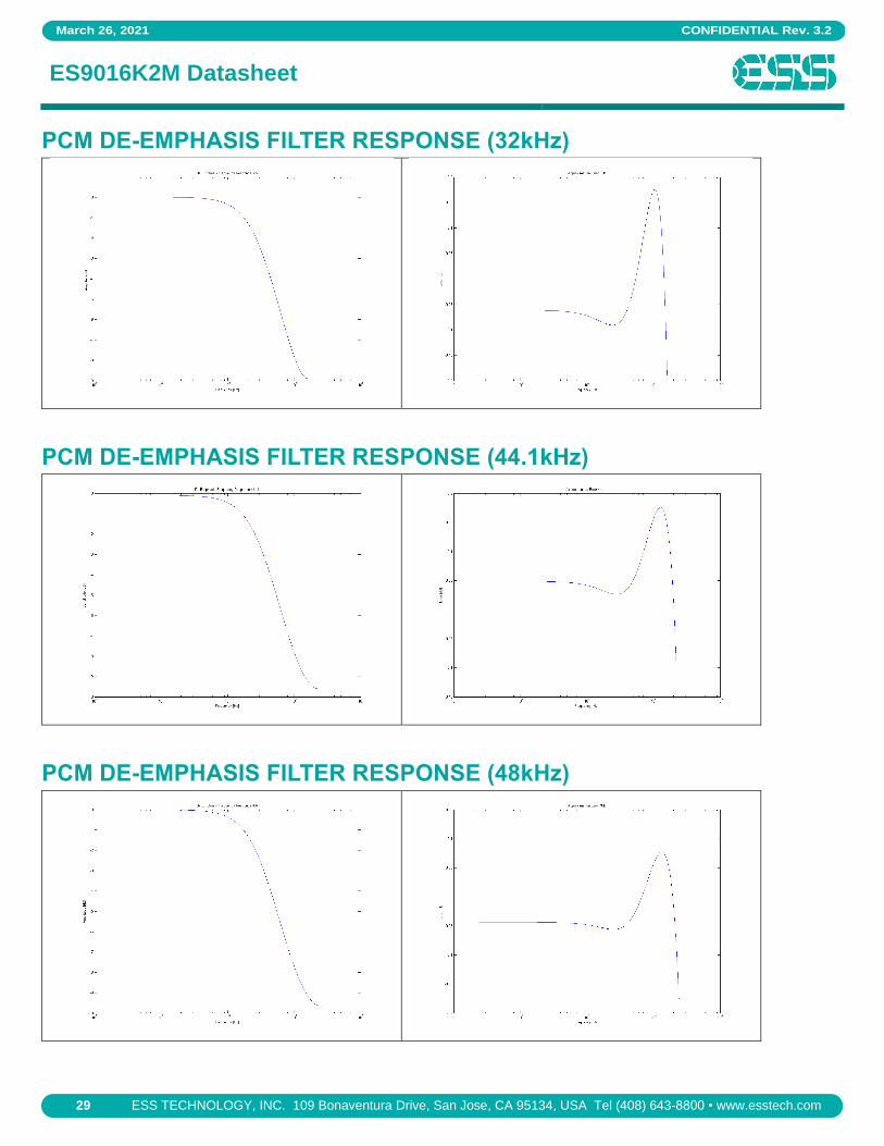
PCM DE-EMPHASIS FILTER RESPONSE (32kHz)
PCM DE-EMPHASIS FILTER RESPONSE (44.1kHz)
PCM DE-EMPHASIS FILTER RESPONSE (48kHz)

CONFIDENTIAL Rev. 3.2 March 26, 2021
ES9016K2M Datasheet
ESS TECHNOLOGY, INC. 109 Bonaventura Drive, San Jose, CA 95134, USA Tel (408) 643-8800 • www.esstech.com
30
PCM FILTER FREQUENCY RESPONSE
dB
dB
dB
Unit: fs

March 26, 2021 CONFIDENTIAL Rev. 3.2
ES9016K2M Datasheet
31 ESS TECHNOLOGY, INC. 109 Bonaventura Drive, San Jose, CA 95134, USA Tel (408) 643-8800 • www.esstech.com
PCM FILTER IMPULSE RESPONSE
Unit: 1/fs (s)

CONFIDENTIAL Rev. 3.2 March 26, 2021
ES9016K2M Datasheet
ESS TECHNOLOGY, INC. 109 Bonaventura Drive, San Jose, CA 95134, USA Tel (408) 643-8800 • www.esstech.com
32
DSD FILTER RESPONSE dB
Unit: DATA_CLK (Hz) / 2822400

March 26, 2021 CONFIDENTIAL Rev. 3.2
ES9016K2M Datasheet
33 ESS TECHNOLOGY, INC. 109 Bonaventura Drive, San Jose, CA 95134, USA Tel (408) 643-8800 • www.esstech.com
28-Pin QFN Mechanical Dimensions

CONFIDENTIAL Rev. 3.2 March 26, 2021
ES9016K2M Datasheet
ESS TECHNOLOGY, INC. 109 Bonaventura Drive, San Jose, CA 95134, USA Tel (408) 643-8800 • www.esstech.com
34
Example 28-Pin QFN Land Pattern
Notes:
1. All dimensions are in millimeters. 2. Thermal vias should be 0.3mm to 0.33mm in diameter, with the barrel plated to 1oz copper. 3. For maximum solder mask in the corners, round the inner corners of each row. 4. Exposed pad should be solder mask defined. 5. Pad width can be reduced to 0.25mm if additional pad to pad clearance is required. 6. For applications where solder loss through vias is a concern, plugging or tenting of the vias should be used. The
solder mask diameter for each via should be 0.1mm larger than the via diameter.

March 26, 2021 CONFIDENTIAL Rev. 3.2
ES9016K2M Datasheet
35 ESS TECHNOLOGY, INC. 109 Bonaventura Drive, San Jose, CA 95134, USA Tel (408) 643-8800 • www.esstech.com
Reflow Process Considerations For lead-free soldering, the characterization and optimization of the reflow process is the most important factor you need to consider. The lead-free alloy solder has a melting point of 217°C. This alloy requires a minimum reflow temperature of 235°C to ensure good wetting. The maximum reflow temperature is in the 245°C to 260°C range, depending on the package size (Table RPC-2). This narrows the process window for lead-free soldering to 10°C to 20°C. The increase in peak reflow temperature in combination with the narrow process window makes the development of an optimal reflow profile a critical factor for ensuring a successful lead-free assembly process. The major factors contributing to the development of an optimal thermal profile are the size and weight of the assembly, the density of the components, the mix of large and small components, and the paste chemistry being used. Reflow profiling needs to be performed by attaching calibrated thermocouples well adhered to the device as well as other critical locations on the board to ensure that all components are heated to temperatures above the minimum reflow temperatures and that smaller components do not exceed the maximum temperature limits (Table RPC-2). To ensure that all packages can be successfully and reliably assembled, the reflow profiles studied and recommended by ESS are based on the JEDEC/IPC standard J-STD-020 revision D.1.
Figure RPC-1. IR/Convection Reflow Profile (IPC/JEDEC J-STD-020D.1)
Note: Reflow is allowed 3 times. Caution must be taken to ensure time between re-flow runs does not exceed the allowed time by the moisture sensitivity label. If the time elapsed between the re-flows exceeds the moisture sensitivity time bake the board according to the moisture sensitivity label instructions.
Manual Soldering: Allowed up to 2 times with maximum temperature of 350 degrees no longer than 3 seconds.

CONFIDENTIAL Rev. 3.2 March 26, 2021
ES9016K2M Datasheet
ESS TECHNOLOGY, INC. 109 Bonaventura Drive, San Jose, CA 95134, USA Tel (408) 643-8800 • www.esstech.com
36
Table RPC-1 Classification reflow profile
Profile Feature Pb-Free Assembly
Preheat/Soak Temperature Min (Tsmin) Temperature Max (Tsmax) Time (ts) from (Tsmin to Tsmax)
150°C 200°C 60-120 seconds
Ramp-up rate (TL to Tp) 3°C / second max.
Liquidous temperature (TL) Time (tL) maintained above TL
217°C 60-150 seconds
Peak package body temperature (Tp)
For users Tp must not exceed the classification temp in Table RPC-2. For suppliers Tp must equal or exceed the Classification temp in Table RPC-2.
Time (tp)* within 5°C of the specified classification temperature (Tc), see Figure RPC-1
30* seconds
Ramp-down rate (Tp to TL) 6°C / second max.
Time 25°C to peak temperature 8 minutes max.
* Tolerance for peak profile temperature (Tp) is defined as a supplier minimum and a user maximum.
Note 1: All temperatures refer to the center of the package, measured on the package body surface that is facing up during assembly reflow (e.g., live-bug).
If parts are reflowed in other than the normal live-bug assembly reflow orientation (i.e., dead-bug), Tp shall be within ± 2°C of the live-bug Tp and still meet the Tc requirements, otherwise, the profile shall be adjusted to achieve the latter. To accurately measure actual peak package body temperatures refer to JEP140 for recommended thermocouple use.
Note 2: Reflow profiles in this document are for classification/preconditioning and are not meant to specify board assembly profiles. Actual board assembly profiles should be developed based on specific process needs and board designs and should not exceed the parameters in Table RPC-1. For example, if Tc is 260°C and time tp is 30 seconds, this means the following for the supplier and the user. For a supplier: The peak temperature must be at least 260°C. The time above 255°C must be at least 30 seconds. For a user: The peak temperature must not exceed 260°C. The time above 255°C must not exceed 30 seconds.
Note 3: All components in the test load shall meet the classification profile requirements.
Table RPC-2 Pb-Free Process – Classification Temperatures (Tc)
Package Thickness Volume mm3, <350 Volume mm3, 350 to 2000 Volume mm3, >2000
<1.6 mm 260°C 260°C 260°C
1.6 mm – 2.5 mm 260°C 250°C 245°C
>2.5 mm 250°C 245°C 245°C
Note 1: At the discretion of the device manufacturer, but not the board assembler/user, the maximum peak package body temperature (Tp) can exceed the
values specified in Table RPC-2. The use of a higher Tp does not change the classification temperature (Tc). Note 2: Package volume excludes external terminals (e.g., balls, bumps, lands, leads) and/or non-integral heat sinks. Note 3: The maximum component temperature reached during reflow depends on package thickness and volume. The use of convection reflow processes
reduces the thermal gradients between packages. However, thermal gradients due to differences in thermal mass of SMD packages may still exist.

March 26, 2021 CONFIDENTIAL Rev. 3.2
ES9016K2M Datasheet
37 ESS TECHNOLOGY, INC. 109 Bonaventura Drive, San Jose, CA 95134, USA Tel (408) 643-8800 • www.esstech.com
ORDERING INFORMATION
Part Number Description Package
ES9016K2M Sabre32® Ultra 32-bit Low Power Stereo Audio DAC 28-pin QFN
The letter K identifies the package type QFN.
Revision History Rev. Date Notes
1.1 March 19, 2014 Update MCLK requirement
1.2 April 15, 2014 Update sync_mode requirement
1.3 May 28, 2014 Update DSD L/R pin assignment. Add THD compensation registers. Update mechanical drawing and add land pattern. Update migration notes
1.4 June 5, 2014 Added SABRE SOUNDTM trademark
1.5 July 28, 2014 Updated ESS’ FAX number. Added medical usage legal disclaimer
1.6 August 28, 2014 Added conditions when an external DVDD regulator is required
1.7 September 8, 2014
Corrected typo on Register#7 Bit [6:5], 3’dX changed to 2’dX. Identified Left and Right channels for Registers #15 and #16 respectively.
Updated DAC output impedance from 781.25 to 806
1.8 September 24, 2014 Added “8 bit, Read-Write Register, Default = 0x00” heading on Register #21. Corrected part number on revision marking diagram, page 3. Removed reference to Right Justified data format that is not supported
1.9 October 16, 2014 Added table to Register #65 description.
2.0 January 8, 2015 Added details on decoupling required for the DVDD core supply. Deleted old revision history from 0.1 to 0.91.
2.1 April 10, 2015 Added notes on the connection of reserved Bits in the device control registers. Added SABRE HiFi logo. Updated ESS’ address and phone number.
2.2 June 10, 2015 Increased typical value of AVCC_L plus AVCC_R from 3mA to 8mA
2.3 December 2, 2016 Correct Recommended Operating Conditions table formatting.
2.4 January 24, 2017 Corrected THD compensation description and Recommended Operating Conditions table formatting.
2.5 January 31, 2017 Remove references to Revision W silicon, clarify I2C address description.
2.6 February 14, 2017 Added description for Registers #2, #3 and #9. Register #65 labeled as GPIO Status. Added register map. Adjusted page number references as needed.
2.7 November 14, 2018 Added Low Power Audio DAC description, removed Advanced Information
2.8 March 13, 2019 Removed ESR capacitor requirement for DVDD. Updated SABRE®, SABRE SOUND® and Sabre32®
2.9 December 30, 2019 Corrected SDA setup time from SCL rising units from “µs” to “ns”.
3.0 April 27. 2020 Updated analog performance
3.1 January 7, 2021 Updated I/V converter filter circuit
3.2 March 26, 2021 Updated Register #9 default value

CONFIDENTIAL Rev. 3.2 March 26, 2021
ES9016K2M Datasheet
ESS TECHNOLOGY, INC. 109 Bonaventura Drive, San Jose, CA 95134, USA Tel (408) 643-8800 • www.esstech.com
38
ESS’ ICs are not intended, authorized, or warranted for use as components in military applications, medical devices or life support systems. ESS assumes no liability whatsoever and disclaims any expressed, implied or statutory warranty for use of ESS IC's in such unsuitable applications. No part of this publication may be reproduced, stored in a retrieval system, transmitted, or translated in any form or by any means, electronic, mechanical, manual, optical, or otherwise, without the prior written permission of ESS Technology, Inc. ESS Technology, Inc. makes no representations or warranties regarding the content of this document. All specifications are subject to change without prior notice. ESS Technology, Inc. assumes no responsibility for any errors contained herein. U.S. patents pending.


![CSc 466/566 [5mm] Computer Security [5mm] 7 : Cryptography](https://img.dokumen.tips/doc/110x75/58a3066e1a28abd1778bb998/csc-466566-5mm-computer-security-5mm-7-cryptography-.jpg)