Embed Size (px)
Citation preview

TECHNICAL UNIVERSITY OF CRETEELECTRICAL AND COMPUTER ENGINEERING DEPARTMENT
TELECOMMUNICATIONS DIVISION
Environmental Scatter Radio Sensors with
RF Energy Harvesting
by
Spyridon-Nektarios Daskalakis
A THESIS SUBMITTED IN PARTIAL FULFILLMENT OFTHE REQUIREMENTS FOR THE MASTER OF SCIENCE OF
ELECTRICAL AND COMPUTER ENGINEERING
July 20, 2016
THESIS COMMITTEE
Associate Professor, Aggelos Bletsas, Thesis SupervisorAssociate Professor, Eftichios Koutroulis
Associate Professor, Matthias Bucher
Abstract
Real-time monitoring of environmental parameters, such as soil moisture, with
wireless sensor networks (WSN), is invaluable for precision agriculture. However,
conventional radios in large-scale deployments are limited by power consumption,
cost and complexity constraints. Scatter-radio, a promising technology, allows the
development of large-scale and low-cost WSN. In this work, the development of
an analog scatter-radio WSN for soil moisture is presented. The WSN consists
of low-cost (6 Euro per sensor), low-power (in the order of 200 µW per sensor)
soil moisture scatter radio sensors, with high communication range (up to 250
m). The WSN utilizes analog frequency modulation (FM) in a bistatic network
architecture, while the sensors operate simultaneously, using frequency division
multiple access (FDMA). The network utilizes an ultra-low cost software-defined
radio reader and proposes a custom microstrip capacitive sensor with a simple
calibration methodology. Overall root mean squared error (RMSE) below 1% is
observed, even for ranges of 250 m. In order to supply the sensor with energy,
a radio frequency (RF) energy harvesting supply system is also presented. The
system collects the unused ambient RF energy from scatter radio emitters and from
one FM station. The design consists of a double diode rectifier with operation in
the two frequencies of 900 MHz and 97.5 MHz, simultaneously, utilizing a low-
cost, lossy FR-4 substrate and a low-complexity rectifier circuit. The achieved
RF-to-DC rectification efficiency was 14.49% and 27.44% at 868 MHz and 97.5
MHz, respectively, and 20 dBm input power. The rectifier was connected to a
commercial boost converter in order to manage and improve the output power
of the rectifier. Finally, the end-to-end efficiency of the system was 21%, at 97.5
MHz and 15 dBm input power. This work offers a concrete example of ultra-
low power and cost wireless sensor networking with (unconventional) novel scatter
radio technology.

Abstract 3
This work was supported by the ERC04-BLASE project, executed in the con-
text of the “Education & Lifelong Learning” Operational Program of the Na-
tional Strategic Reference Framework (NSRF), General Secretariat for Research
& Technology (GSRT), funded through European Union-European Social Fund
and Greek national funds. It was also supported by Onassis Foundation gradu-
ate studies 2015/16 scholarship and by the COST Action IC1301 WiPE Wireless
Power Transmission for Sustainable Electronics.
Thesis Supervisor: Associate Professor Aggelos Bletsas

4
Acknowledgements
I would like to thank my family and my friends for the invaluable moral support
they provided. My parents, deserve mention, although I couldn’t possibly write
enough. I would also like to thank all members of Technical Univ. of Crete,
school of ECE Fab/Telecom Lab and especially my advisor and mentor Aggelos
Bletsas, who has offered me all the guidance I needed and facilitated my academic
growth, throughout my course as a graduate student. Moreover, special thanks to
Dr. Stylianos D. Assimonis who introduced me to the world of electromagnetism
and energy harvesting. Finally I would like to thank Alexander S. Onassis Public
Benefit Foundation for the 2015/16 scholarship program during my MSc studies.

5
Table of Contents
Table of Contents . . . . . . . . . . . . . . . . . . . . . . . . . . . . . . . 5
List of Figures . . . . . . . . . . . . . . . . . . . . . . . . . . . . . . . . . 7
List of Tables . . . . . . . . . . . . . . . . . . . . . . . . . . . . . . . . . 10
1 Introduction . . . . . . . . . . . . . . . . . . . . . . . . . . . . . . . . 11
1.1 Scatter Radio Principles . . . . . . . . . . . . . . . . . . . . . . . . 13
2 Sensors Design and Implementation . . . . . . . . . . . . . . . . . 16
2.1 Sensor & C2F Converter . . . . . . . . . . . . . . . . . . . . . . . . 17
2.1.1 50% Duty Cycle Circuit Analysis . . . . . . . . . . . . . . 18
2.1.2 Capacitive Sensor Design and Simulations . . . . . . . . . . 20
2.2 Scatter Radio Antenna/Front-end . . . . . . . . . . . . . . . . . . 23
2.3 Multiple Access . . . . . . . . . . . . . . . . . . . . . . . . . . . . . 24
2.4 Power Consumption & Tradeoff . . . . . . . . . . . . . . . . . . . . 27
2.5 Ultra-Low Cost WSN Receiver . . . . . . . . . . . . . . . . . . . . 29
2.6 Calibration . . . . . . . . . . . . . . . . . . . . . . . . . . . . . . . 31
2.7 Experimental Results . . . . . . . . . . . . . . . . . . . . . . . . . 33
3 Dual Band RF Harvesting & Low-Power Supply System . . . . 38
3.1 Rectifier . . . . . . . . . . . . . . . . . . . . . . . . . . . . . . . . . 39
3.1.1 Rectifier Design and Analysis . . . . . . . . . . . . . . . . . 39
3.2 Antenna Design . . . . . . . . . . . . . . . . . . . . . . . . . . . . 42
3.3 Boost Converter . . . . . . . . . . . . . . . . . . . . . . . . . . . . 42
3.3.1 End-to-End Efficiency . . . . . . . . . . . . . . . . . . . . . 45

Table of Contents 6
4 Conclusions . . . . . . . . . . . . . . . . . . . . . . . . . . . . . . . . . 49
4.1 Conclusion . . . . . . . . . . . . . . . . . . . . . . . . . . . . . . . 49
4.2 Future Work . . . . . . . . . . . . . . . . . . . . . . . . . . . . . . 49
5 Appendix . . . . . . . . . . . . . . . . . . . . . . . . . . . . . . . . . . 50
5.1 Matlab Receiver Code . . . . . . . . . . . . . . . . . . . . . . . . . 50
5.2 PCBs . . . . . . . . . . . . . . . . . . . . . . . . . . . . . . . . . . 53
Bibliography . . . . . . . . . . . . . . . . . . . . . . . . . . . . . . . . . . 56

7
List of Figures
1.1 Bistatic soil moisture scatter radio WSN. There could be multiple
carrier emitters and one software-defined radio (SDR) reader. . . . . 11
1.2 Scatter radio principles: The low power RF switch “ADG902” alter-
nates the termination loads Z1 and Z2 of the antenna (correspond-
ing to reflection coefficients Γ1, Γ2, respectively) with frequency
Fsw. When the illuminating carrier frequency is Fc, two new sub-
carrier frequencies Fc ± Fsw appear in the spectrum. Difference
|Γ1−Γ2| should be maximized; however, practical constraints (e.g.,
parasitics) restrict such maximization. . . . . . . . . . . . . . . . . 12
1.3 Bistatic topology of a scatter radio link; emitter produces the carrier
signal which is modulated by sensor nodes and finally, the reflected
signal is received by a software defined radio (SDR) reader. det and
dtr denote emitter-to-tag and tag-to-reader distance, respectively.
Notice that in this work, one emitter illuminates multiple tags, si-
multaneously. . . . . . . . . . . . . . . . . . . . . . . . . . . . . . . 14
2.1 The analog backscatter sensor node schematic. Each node consists
of the capacitive soil moisture sensor to be inserted in the soil, the
timer module that converts the variable capacitance to frequency
(C2F) and the scatter radio front end. The variable frequency signal
controls the antenna RF switch. The node is supplied by a voltage
reference circuit. . . . . . . . . . . . . . . . . . . . . . . . . . . . . 16
2.2 The output of sensor node is displayed on oscilloscope and its scat-
tered signal (subcarrier) is displayed on spectrum analyser. For the
backscatter communication was used a 868 MHz single carrier emitter. 19

List of Figures 8
2.3 Eagle designs of tags. Intedigatated capacitive sensor (Up, Left)
and parallel Plate capacitive sensor (Up, Right). Printed sircuit
boards (PCBs) with solder mask (Down). . . . . . . . . . . . . . . . 21
2.4 ADS material definition preview. . . . . . . . . . . . . . . . . . . . 22
2.5 Soil moisture sensor capacitance versus frequency. ADS simulation
for water case. . . . . . . . . . . . . . . . . . . . . . . . . . . . . . . 23
2.6 The fabricated sensor node (right). The green solder mask has
been used as sensor insulation. Capacitive sensor and antenna/s-
catter radio front-end are fabricated on low-cost FR-4 substrate.
The Realtek RTL software-defined radio (SDR) reader, depicted on
the (left), is ultra-low cost on the order of 7 Euro. . . . . . . . . . . 25
2.7 Inlay figure with concept and frequency-division multiple access of
simultaneously operating multiple tags; each tag operates in a dif-
ferent frequency band, while guard bands avoid adjacent-channel
interference. Measured sensor network spectrum for sensors #1− 18. 26
2.8 Total power consumption versus sensor subcarrier frequency. . . . . 28
2.9 PCB picture (Up) and high level block diagram (Down) of the RTL-
SDR. . . . . . . . . . . . . . . . . . . . . . . . . . . . . . . . . . . . 29
2.10 Measured soil moisture (%) characteristic and polynomially-fitted
function versus frequency and temperature for sensor #8. The data
measurements were 226 sets of soil moisture, temperature and out-
put frequency samples. . . . . . . . . . . . . . . . . . . . . . . . . . 32
2.11 Measured soil moisture (%) characteristic and fitted function versus
frequency for sensor #8 for fixed environmental temperature (18.4C). 33
2.12 18 Soil Moiture Sensor Tag Designs. . . . . . . . . . . . . . . . . . . 34
2.13 Bistatic soil moisture sensor network demonstration; capacitive soil
moisture sensor in installed into the ground, while scatter radio
antenna is well above ground and being illuminated by the carrier
emitter (E), while backscattered signal from various tags is received
by the reader (R). . . . . . . . . . . . . . . . . . . . . . . . . . . . . 35
2.14 Simultaneous and continuous soil moisture sensing from 8 tags, as
a function of time, using the proposed scatter radio sensor network. 36

List of Figures 9
2.15 Testing outdoors the communication range of the specific bistatic
analog backscatter architecture. . . . . . . . . . . . . . . . . . . . . 37
3.1 The double diode rectifier design. . . . . . . . . . . . . . . . . . . . 38
3.2 The fabricated top layer of the rectifier. . . . . . . . . . . . . . . . . 39
3.3 Reflection coefficient at the input of rectifier. . . . . . . . . . . . . . 40
3.4 Rectifier efficiency versus total power input at 868 MHz. . . . . . . 41
3.5 Rectifier efficiency versus total power input at 97.5 MHz. . . . . . . 42
3.6 Rectifier efficiency versus frequency for different power inputs. . . . 43
3.7 Rectifier efficiency for 868 MHz versus load for different power inputs. 44
3.8 Rectifier efficiency for 97.5 MHz versus load for different power inputs. 45
3.9 Measured rectifier output open circuit voltage for 97.5 MHz and 868
MHz. . . . . . . . . . . . . . . . . . . . . . . . . . . . . . . . . . . 46
3.10 The fabricated multi-band antenna. . . . . . . . . . . . . . . . . . . 46
3.11 Reflection coefficient of the multi-band antenna. . . . . . . . . . . . 47
3.12 Boost converter schematic with the low-power BQ25504. . . . . . . 47
3.13 Measurement setup with rectifier, signal generator, boost converter
and MOSFET transistors. . . . . . . . . . . . . . . . . . . . . . . . 48
3.14 Boost converter input (VIN DC) and output (VBAT ) voltage mea-
surement for Pin = −15 dBm and F = 97.5 MHz. Voltage VBAT is
the voltage across 100 uF capacitor, and VIN DC is the open circuit
voltage of rectifier output. . . . . . . . . . . . . . . . . . . . . . . . 48
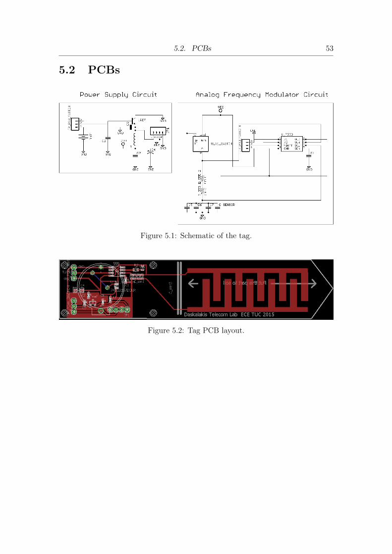
5.1 Schematic of the tag. . . . . . . . . . . . . . . . . . . . . . . . . . . 53
5.2 Tag PCB layout. . . . . . . . . . . . . . . . . . . . . . . . . . . . . 53
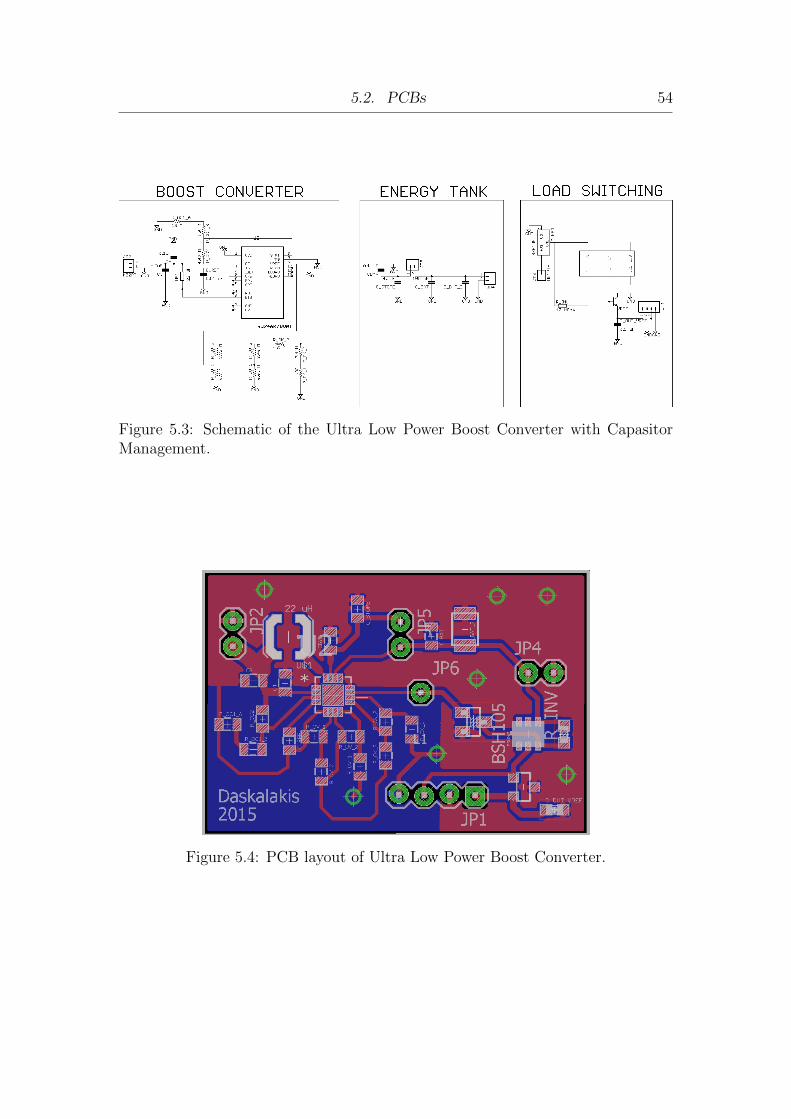
5.3 Schematic of the Ultra Low Power Boost Converter with Capasitor
Management. . . . . . . . . . . . . . . . . . . . . . . . . . . . . . . 54
5.4 PCB layout of Ultra Low Power Boost Converter. . . . . . . . . . . 54
5.5 PCB of Ultra Low Power Boost Converter. . . . . . . . . . . . . . . 55

10
List of Tables
2.1 “Interdigitated” sensor measurement and simulation data in (pF). . 23
2.2 “Parallel plates” sensor measurement and simulation data in pF. . . 24
2.3 Power consumption example for two sensor nodes. . . . . . . . . . . 28
2.4 Calibration function and fitting error. . . . . . . . . . . . . . . . . . 31
2.5 Communication Accuracy. . . . . . . . . . . . . . . . . . . . . . . . 37

11
Chapter 1
Introduction
Nowadays, modern agriculture applications necessitate cheap, effective, low main-
tenance and low-cost wireless telemetry for various environmental parameters [1],
such as environmental humidity, soil moisture, barometric pressure and air/leaf
stomata temperature [2–5]. Continuous and dense environmental monitoring is
critical for optimal crop and water management techniques and thus, wireless sen-
sor network (WSN) technologies for microclimate monitoring in extended areas,
are indispensable within this topic [1]. One important environmental variable that
needs careful monitoring, especially in agriculture and water management applica-
tions, is percentage soil moisture (%SM). Prior art has offered novel soil moisture
capacitive sensors integrated with discrete wireless radio module [6], [7] or discrete
processing chip [8], including ink-jet fabrication designs.
Soil Moisture Sensor
Backscattering
SDR Reader
CarrierEmitter 3
CarrierEmitter 2
CarrierEmitter 1
Figure 1.1: Bistatic soil moisture scatter radio WSN. There could be multiplecarrier emitters and one software-defined radio (SDR) reader.

Chapter 1. Introduction 12
IC ADG902
ZaZ1
Z2
Fsw
Control circuitAntenna RF ront-endf Frequency Spectrum
F + Fc swFcF - Fc sw
LOADS
Figure 1.2: Scatter radio principles: The low power RF switch “ADG902” alter-nates the termination loads Z1 and Z2 of the antenna (corresponding to reflectioncoefficients Γ1, Γ2, respectively) with frequency Fsw. When the illuminating carrierfrequency is Fc, two new subcarrier frequencies Fc ± Fsw appear in the spectrum.Difference |Γ1 − Γ2| should be maximized; however, practical constraints (e.g.,parasitics) restrict such maximization.
Conventional WSNs consist of a network of nodes (possibly in a mesh archi-
tecture), transferring monitored environmental data to a base station. Each node
typically employs a Marconi-type radio (e.g. ZigBee/Lora-type), controlled by a
microcontroller unit (MCU) and the sensors. However, large-scale deployments of
conventional WSN technology are uncommon, due to power consumption, instal-
lation and maintenance cost. Work in [9] is one rare case of large-scale, outdoor
demonstration, with packaging/long-term deployment cost per wireless sensor in
the order of 50 Euro.
In order to address power consumption and cost per sensor constraints, scatter
radio has recently attracted interest for wireless sensing development (Fig. 1.1).
In the first work for scatter radio networking [10], it is showed that, using scatter
radio, the front end of each sensor is simplified to a reflector that modulates in-
formation on the sensor’s antenna-load reflection coefficient; in scatter radio, com-
munication is performed by means of reflection, where signal conditioning such as
filtering, mixing or amplification at the sensor/tag are typically avoided; in that
way, low power consumption is needed, offering opportunities for battery-less op-
eration [11, 12], e.g., each sensor can be powered using ambient radio frequency
(RF) energy with appropriate rectifiers (e.g., [13–15]) or using multiple kinds of
ambient energy sources, such as RF and solar energy, simultaneously (e.g., [16]).
1.1. Scatter Radio Principles 13
A RF rectifier example is presented below, in this work. Sensor designs with scat-
ter radio typically exploit variations of sensor’s antenna properties [17], based on
the environmental parameter under monitoring, such as the (mechanical) shape
(e.g., [18]) or the dielectric constant (e.g., [19]); chip-less designs typically include
appropriately-designed antenna loads with delay lines (e.g., work in [20] and refer-
ences therein); another way to construct scatter radio signal reflectors is by using a
switch, connecting sensor’s antenna to different loads. Elevating the above princi-
ples from sensing to networking of several, simultaneously operating, scatter radio
sensors is not trivial and emerges as a challenging topic of research.
Work in [21] offered frequency-modulated scatter radio signals with soil mois-
ture information and duty-cycled operation that reduced the operating bandwidth,
while experimental results were reported for only two sensors and commodity soft-
ware defined radio (with cost in the order of 1000 Euro). The tag-to-reader com-
munication range was in the order of 100 meter. In this work, 50% duty-cycle
of frequency modulated soil moisture is achieved with a new circuit, which also
reduces the overall power consumption; 50% duty cycle is crucial for getting rid
of even-order harmonics and thus, enhancing the available bandwidth for multiple
scatter radio sensors simultaneous access [22]. Moreover, this work offers different
and more accurate sensor calibration, experimental results for multiple sensors,
ranges in the order of 250 meter with ultra-low cost, portable SDR (that costs 7
Euro), while scalability issues are further examined.
1.1 Scatter Radio Principles
Scatter radio communication, known from 1948 [23], is currently exploited in the
radio frequency identification (RFID) industry. Communication is implemented
with an antenna, a control circuit and a radio frequency (RF) switch between them.
The switch alternatively terminates the tag/sensor antenna between (usually two)
loads Z1 and Z2 (Fig. 1.2). The control circuit is responsible for the modulation
operation. Tag/sensor antenna S11 parameter (i.e., reflection coefficient Γ), asso-
ciated with each antenna terminating load, is modified when the antenna load is
changed. The different termination loads offer different reflection coefficients, (Γ1
1.1. Scatter Radio Principles 14
Carrier Emitter
det dtr
Sensor SDR Reader
Figure 1.3: Bistatic topology of a scatter radio link; emitter produces the carriersignal which is modulated by sensor nodes and finally, the reflected signal is re-ceived by a software defined radio (SDR) reader. det and dtr denote emitter-to-tagand tag-to-reader distance, respectively. Notice that in this work, one emitterilluminates multiple tags, simultaneously.
and Γ2) according to the following [24–28]:
Γi =Zi − Z∗aZi + Za
, (1.1)
with i = 1, 2 and Za denoting the antenna impedance. Therefore, amplitude and
phase of the carrier signal - induced at the sensor antenna -are modulated and
the signal is reflected (scattered) back towards a receiver. As a result, when a
continuous wave (CW) with frequency Fc is incident on the sensor antenna, which
is alternatively terminated between two loads at a rate Fsw, two new subcarrier
frequencies appear in the spectrum (Fig. 1.2); their frequency values are given
by [10]:
Fsub,1 = Fc + Fsw, (1.2)
Fsub,2 = Fc − Fsw. (1.3)
While scatter-radio principles have been restricted to communication ranges of up
to a few meter [29–31], a novel scatter radio sensor network (WSN) for relative
humidity (%RH) measurements was presented in [32]. That WSN consisted of
low-power and low-cost analog designs of wireless transmitters sensor nodes/tags

1.1. Scatter Radio Principles 15
1 with scatter radio and extended communication ranges. Each tag employed
bistatic semi-passive scatter radio principles [33], [34]. In order to address the small
communication range problem, the WSN utilized the bistatic topology (where the
carrier emitter was placed in a different location from the reader) and semi-passive
(i.e., battery-assisted) tags. The utilization of the bistatic topology is illustrated
in Fig. 1.3. Using the above concepts, it was shown possible to implement large-
scale networks, comprising of low-cost sensor/tags, a few emitters operating at the
European RFID band (865 − 868 MHz) [35] and a single software-defined radio
(SDR) receiver, detecting the backscattered signals.
The first part of this work describes the development of a bistatic scatter radio
WSN, that measures soil moisture percentage (%SM) with analog, frequency mod-
ulation (FM) principles and ranges in the order of 250 meter. In sharp contrast
to prior art, this work offers a) custom capacitive sensing, b) soil moisture sensing
and networking of multiple sensors (with corroborating experimental results), c)
reception with ultra-low cost software-defined radio (SDR) that costs only a few
Euro and d) special modulation design that offers scatter radio modulation signals
with 50% duty cycle; the latter will be shown to be important for signal-to-noise
ratio improvements at the SDR receiver, as well as for network scalability pur-
poses. In second part, a RF energy harvesting system for sensor power supply is
presented. The system uses RF energy from scatter radio emitters and one FM
station in order to collect the unused ambient energy.
For the first part, Section 2.1 offers the design and implementation of the
scatter radio sensor circuit, multiple access capability and power consumption
tradeoff. Section 2.5 offers the SDR receiver design, based on a 8-bit ultra-low cost
SDR, Section 2.6 describes the simple calibration procedure and Section 2.7 offers
the experimental results, including a relevant network demonstration and bistatic
range measurements. The second part is summarized as follows: in Section 3.1,
a rectifier circuit is presented. In Section 3.2, a dual band printed antenna is
described. In Section 3.3, the use of a commercial DC-DC converter is described
and the overall end-to-end efficiency is derived. Finally, overall work is concluded
in Chapter 4.
1In line with standard RFID terminology, the terms “tag”,“node” or “sensor node” will beused interchangeably.

16
Chapter 2
Sensors Design and
Implementation
THRESHOLD
CONTROLOUTPUT
VCCRESET
GND GND
GND
GND
Bow-Tie Antenna
ADG902
Capacitive Sensor
Fsw
CSS 555
Vref
1.8V
Copper
Fr-4
Timer modulePower SupplyRF Front end
DISCARGETRIGGER
Z1Z2
Fsw
IC
IC
Figure 2.1: The analog backscatter sensor node schematic. Each node consists ofthe capacitive soil moisture sensor to be inserted in the soil, the timer module thatconverts the variable capacitance to frequency (C2F) and the scatter radio frontend. The variable frequency signal controls the antenna RF switch. The node issupplied by a voltage reference circuit.
The design target of the tags is to produce voltage pulses of fundamental fre-
quency that depends on the %SM value and control the rate with which the an-
tenna termination loads are alternated. For this purpose, the circuit diagram of
Fig. 2.1 was designed, consisting of a custom capacitive soil moisture sensor, the
capacitance-to-frequency converter (C2F), the power supply circuit and the scatter
radio front-end.
2.1. Sensor & C2F Converter 17
2.1 Sensor & C2F Converter
A single astable multi-vibrator circuit with “555” timer functioned as the capacitance-
to-frequency converter. The timer was the ultra low power monolithic CSS555 [36]
with minimum current consumption of 5 uA at 1.2 V. The timer was connected
to a resistor-capacitor network of R2, Cp and to the custom, microstrip capacitive
sensor Csm (Fig. 2.1). The capacitive sensor consisted of two isolated conductive
plates, separated by a narrow gap, on low cost FR-4 substrate with thickness 1.5
mm and and dielectric constant εr = 4.6; waterproofness was facilitated using
the green solder mask as insulation. The followed capacitance sensor design is
equivalent to a number of co-planar plate capacitors, inserted in parallel into the
soil, which alters the dielectric constant; if soil is moist (high %SM), the capacitor
will contain more water, resulting to higher capacitance (i.e., high Csm), while
dry soil offers lower capacitance. More informations about the sensor design and
simulations are available below 2.1.2.
The fundamental frequency Fsw of the pulse depends on the resistor and the
capacitor, connected to the TRIGGER and THRESHOLD pins of the “555” timer.
As depicted in Fig. 2.1 (arrows), the parallel capacitors (Cp and Csm) are period-
ically charged (green arrows) and discharged (brown arrows) through R2 and an
electronic, single-pole single-throw (SPST) switch (SW). The SW is open when
timer output is in logic “low”, so there is no leakage current through the SW
loop and has been placed in order to reduce consumption, while attaining pulses
with duty cycle of 50%; the latter is a fundamental difference compared to other
capacitance-to-frequency converters in the literature (e.g., [32]). The timer output
square wave pulse is offered with fundamental frequency given by:
Fsw =1
2 ln(2)R2(Cp + Csm). (2.1)
According to [37], the power of the fundamental subcarrier frequency of the
scattered signal is given by:
P (a) =
[A√
2
πsin(πD)
]2
, (2.2)

2.1. Sensor & C2F Converter 18
where A is the peak-to-peak amplitude of the pulse signal and D is the duty cycle;
thus, the backscattered signal power will be increased when D approaches the
value of 50%. Using a single analog switch (SW in Fig. 2.1) and only one resistor
(R2) in the typical astable multi-vibrator circuit, the duty cycle of the produced
pulse is calculated as follows:
D =R2
2R2
= 50%. (2.3)
The capitulation procedure is explained in the next subsection 2.1.1. According
to its Fourier series analysis, a 50% duty-cycle square pulse consists of odd order
harmonics of the fundamental frequency, i.e., even order harmonics are not present.
Therefore, square waves without 50% duty-cycle occupy additional bandwidth,
limiting the capacity of the designed network in a specific frequency band.
2.1.1 50% Duty Cycle Circuit Analysis
If the overall capacitance is denoted as C = Cp +Csm, the time, during which the
C is charged from 1/3VCC to 2/3VCC, is equal to the time that the output is high.
The time is denoted as THIGH. Voltage across C at any instant during charging
period is given as,
Vcap = VCC(1− et
R×C ). (2.4)
Time t1 when C is charged from 0 to 1/3VCC, is calculated from:
1
3VCC = VCC(1− e−
t1R×C ), (2.5)
t1 = R× C × ln2
3= 0.405R× C. (2.6)
Time t2 when C is charged from 0 to 2/3VCC is calculated from:
2
3VCC = VCC(1− e−
t2R×C ), (2.7)

2.1. Sensor & C2F Converter 19
Figure 2.2: The output of sensor node is displayed on oscilloscope and its scat-tered signal (subcarrier) is displayed on spectrum analyser. For the backscattercommunication was used a 868 MHz single carrier emitter.
t2 = R× C × ln1
3= 1.0986R× C. (2.8)
So the time THIGH, when the capacitor is charged from 1/3VCC to 2/3VCC is taken
by:
THIGH = (t2 − t1) = (1.0986− 0.405)R× C = 0.693R× C. (2.9)
If R = R2,
THIGH = 0.693R2 × C (2.10)
with R2 is in Ohm and C in F. The time, when the capacitor is discharged from
1/3VCC to 2/3VCC, is equal to the time that the output is low. Time is given as
TL0W . Voltage across the capacitor at any instant during discharging period is
given as:
Vd =2
3VCC × e−
tR2×C . (2.11)

2.1. Sensor & C2F Converter 20
Substituting V d = 1/3VCC and t = TL0W in above equation,
TLOW = 0.693R2 × C. (2.12)
Overall period of oscillation is,
Tsw = THIGH + TLOW = 0.693× 2R2 × C. (2.13)
The frequency of oscillation being the reciprocal of the overall period of oscillation
Tsw is given as:
Fsw =1
Tsw=
1.44
2R2 × C. (2.14)
Equation indicates that the frequency of oscillation is independent of the supply
voltage VCC. Often the term duty cycle (D) is used in conjunction with the astable
multivibrator circuit. The duty cycle, the ratio of the time tc during which the
output is high to the total time period Tsw is given as:
D =tcTsw× 100 =
R2
2R2
× 100 = 50%. (2.15)
In Fig. 2.2 is obvious that the duty cycle of a tag is 50% and the Fsw is 35.9
kHz. In spectrum analyser is depicted that, there aren’t even order harmonics,
there is only the carrier (868 MHz) and odd order harmonics.
2.1.2 Capacitive Sensor Design and Simulations
The sensor consists of two isolated conductive plates, separated by a narrow gap.
The assembly must be waterproof, as it will be in contact with moist soil for
extended periods of time. As luck would have it, there is an inexpensive technology
that enables us to build isolated conductors in arbitrary shapes with ridiculously
small tolerances. This technology is printed circuit board fabrication with solder
mask.
This work presents two different capacitive sensor designs. For the first, was
designed a custom printed circuit board (PCB) that contains a number of co-planar

2.1. Sensor & C2F Converter 21
Figure 2.3: Eagle designs of tags. Intedigatated capacitive sensor (Up, Left) andparallel Plate capacitive sensor (Up, Right). Printed sircuit boards (PCBs) withsolder mask (Down).
plate capacitors in parallel, called “interdigitated” (Fig. 2.3, left). Capacitance
sums in parallel, so this will lead to a larger capacity of the entire assembly and
therefore a larger capacity swing when the dielectric changes. For the second
design, called “parallel plates” (Fig. 2.3, right), there are two parallel plates and a
small gap between them. For both of them, there is the necessity to be measured
the dielectric constant (εr) of the surrounding medium, and not of the PCB FR-
4 fibreglass. In Fig. 2.3 are depicted the sensors as designed in Eagle software.
The entire tag is about 125 mm long and 27 mm wide. Sensors dimensions are
about 55 mm long and 20 mm wide. On the reverse side of the PCB there are
not traces of sensor. All PCBs sport a pointy tip for easy insertion into soil. Note
the relatively large gap (2-3 mm) between the plates. The capacity is actually
inversely proportional to the gap.
The sensors, covered by solder mask, were simulated and measured. Results
was useful for the WSN design. For the simulations was used the Advanced Design
System (ADS) by Agilent. Microwave analysis was performed in order to estimate
the capacitance. Two cases of simulation were investigated: initial, the capacitors
was surrounded by air (air-case) and next by water (water-case). Two models of
the sensor (“interdigitated” and “parallel plates”) were designed in ADS with same
dimensions as Eagle designs. Above FR-4 substrate, a water proof layer (green
solder mask) was added with thickness 75 µm, εr = 3.56 and tanδ = 0.038. Water
proof material, and FR-4 was surrounded by air (εr = 1, thickness 100 mm) and
water (εr = 78.2, tanδ = 0.4 and thickness 100 mm) for air-case and water-case,
2.1. Sensor & C2F Converter 22
Figure 2.4: ADS material definition preview.
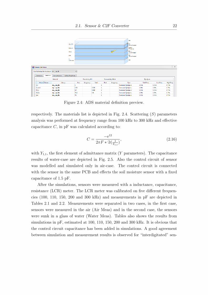
respectively. The materials list is depicted in Fig. 2.4. Scattering (S) parameters
analysis was performed at frequency range from 100 kHz to 300 kHz and effective
capacitance C, in pF was calculated according to:
C =−e12
2πF ∗ =( 1Y1,1
), (2.16)
with Y1,1, the first element of admittance matrix (Y parameters). The capacitance
results of water-case are depicted in Fig. 2.5. Also the control circuit of sensor
was modelled and simulated only in air-case. The control circuit is connected
with the sensor in the same PCB and effects the soil moisture sensor with a fixed
capacitance of 1.5 pF.
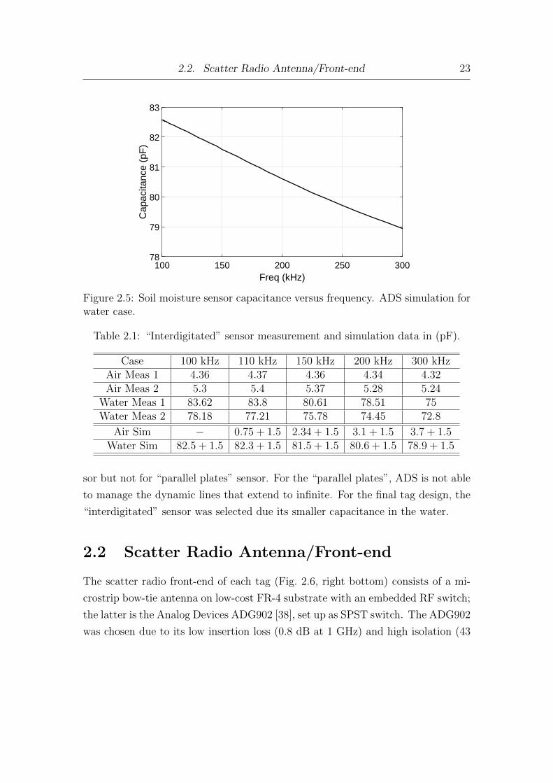
After the simulations, sensors were measured with a inductance, capacitance,
resistance (LCR) meter. The LCR meter was calibrated on five different frequen-
cies (100, 110, 150, 200 and 300 kHz) and measurements in pF are depicted in
Tables 2.1 and 2.2. Measurements were separated in two cases, in the first case,
sensors were measured in the air (Air Meas) and in the second case, the sensors
were sunk in a glass of water (Water Meas). Tables also shows the results from
simulations in pF, estimated at 100, 110, 150, 200 and 300 kHz. It is obvious that
the control circuit capacitance has been added in simulations. A good agreement
between simulation and measurement results is observed for “interdigitated” sen-
2.2. Scatter Radio Antenna/Front-end 23
Freq (kHz)100 150 200 250 300
Cap
acita
nce
(pF
)
78
79
80
81
82
83
Figure 2.5: Soil moisture sensor capacitance versus frequency. ADS simulation forwater case.
Table 2.1: “Interdigitated” sensor measurement and simulation data in (pF).
Case 100 kHz 110 kHz 150 kHz 200 kHz 300 kHzAir Meas 1 4.36 4.37 4.36 4.34 4.32Air Meas 2 5.3 5.4 5.37 5.28 5.24
Water Meas 1 83.62 83.8 80.61 78.51 75Water Meas 2 78.18 77.21 75.78 74.45 72.8
Air Sim − 0.75 + 1.5 2.34 + 1.5 3.1 + 1.5 3.7 + 1.5Water Sim 82.5 + 1.5 82.3 + 1.5 81.5 + 1.5 80.6 + 1.5 78.9 + 1.5
sor but not for “parallel plates” sensor. For the “parallel plates”, ADS is not able
to manage the dynamic lines that extend to infinite. For the final tag design, the
“interdigitated” sensor was selected due its smaller capacitance in the water.
2.2 Scatter Radio Antenna/Front-end
The scatter radio front-end of each tag (Fig. 2.6, right bottom) consists of a mi-
crostrip bow-tie antenna on low-cost FR-4 substrate with an embedded RF switch;
the latter is the Analog Devices ADG902 [38], set up as SPST switch. The ADG902
was chosen due to its low insertion loss (0.8 dB at 1 GHz) and high isolation (43

2.3. Multiple Access 24
Table 2.2: “Parallel plates” sensor measurement and simulation data in pF.
Case 100 kHz 110 kHz 150 kHz 200 kHz 300 kHzAir Meas 5.78 5.85 5.79 5.8 5.77
Water Meas 554.7 544 505 445 370
Air Sim − − 1.4 + 1.5 1.88 + 1.5 2.2 + 1.5Water Sim 88 + 1.5 87.8 + 1.5 86.8 + 1.5 85.5 + 1.5 83.4 + 1.5
dB at 1 GHz). The front-end design was tuned around 868 MHz, according to the
maximization principles in [28].
With the significant assistance of Dr. Stylianos D. Asimonis, a bowtie antenna
for each sensor design was adopted, due to its omnidirectional attributes (at the
vertical to its axe level) and the ease of fabrication, with nominal gain of G = 1.8
dBi. Fig. 2.6 offers dimensions. Such antenna is appropriate for the bistatic scatter
radio topology, while a different printed antenna with higher gain could increase the
ranging distance in the bistatic topology; however appropriate alignment during
installation could be needed in that case.
Five different scatter radio front-ends was designed and tested in this work.
Two conventional designs were constructed (the RF switch PCB was separated
from the antenna) with BF1118 and ADG919 RF switch. Also three novel designs
(custom, coplanar bow tie antenna with the embedded RF switch in the same PCB)
were constructed with BF1118, ADG919, and ADG902, RF switch. In order to be
measured the performance, bi-static topology was used and spectrum analyser was
the reader. The average captured power was measured after 500 iterations. The
distance emitter-to-tag and tag-to-reader was 3 m and 9 m, respectively and the
measurement took place into the ECE building. Switchers with better insertion
loss and high isolation (ADG902 and ADG919), embedded on novel designs, had
the better performance. As the final selection, was used the ADG902 due to its
smaller cost.
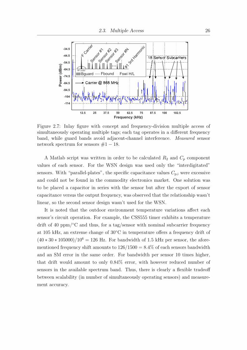
2.3 Multiple Access
Simultaneous, collision-free operation of multiple, receiver-less sensors is facilitated
with frequency-division multiple access principles [22], [10], [32]; every tag is as-

2.3. Multiple Access 25
TIMER MODULE
RF FRONT ENDRF SWITCH
RTL SDR DVB-TUSB DONGLE
DIPOLE ANTENNA75 Ohm 868 MHz
SOIL MOISTURESESNORCAPACITIVE
CR 2032 BATTERY
25cm
48cm
Figure 2.6: The fabricated sensor node (right). The green solder mask has beenused as sensor insulation. Capacitive sensor and antenna/scatter radio front-endare fabricated on low-cost FR-4 substrate. The Realtek RTL software-definedradio (SDR) reader, depicted on the (left), is ultra-low cost on the order of 7 Euro.
signed a distinct frequency band (bandwidth), within which the switching rate
(i.e., subcarrier frequency) of each tag’s antenna load can vary. Fig. 2.7 illustrates
the concept with both conceptual and experimental data.
Let F Lsw,i and FH
sw,i denote the subcarrier frequency output of the i-th tag for
lowest and highest frequency, produced by the C2F converter when the %SM is
100 and 0, respectively. The required bandwidth Bi depends on the above two
frequencies and is calculated as:
Bi = FHsw,i − F L
sw,i. (2.17)
Assuming that CL, CH are the Csm sensor capacitance for 0%, 100% SM, respec-
tively, the Cp,i and R2,i components of i-th tag are calculated according to (2.1),
(2.17) as:
Cp,i =−Bi CL + F L
sw,i (CH − CL)
Bi
, (2.18)
R2,i =Bi
2 ln(2) F Lsw,i (CH − CL) (F L
sw,i +Bi). (2.19)
2.3. Multiple Access 26
Figure 2.7: Inlay figure with concept and frequency-division multiple access ofsimultaneously operating multiple tags; each tag operates in a different frequencyband, while guard bands avoid adjacent-channel interference. Measured sensornetwork spectrum for sensors #1− 18.
A Matlab script was written in order to be calculated R2 and Cp component
values of each sensor. For the WSN design was used only the “interdigitated”
sensors. With “parallel-plates”, the specific capacitance values Cp,i were excessive
and could not be found in the commodity electronics market. One solution was
to be placed a capacitor in series with the sensor but after the export of sensor
capacitance versus the output frequency, was observed that the relationship wasn’t
linear, so the second sensor design wasn’t used for the WSN.
It is noted that the outdoor environment temperature variations affect each
sensor’s circuit operation. For example, the CSS555 timer exhibits a temperature
drift of 40 ppm/C and thus, for a tag/sensor with nominal subcarrier frequency
at 105 kHz, an extreme change of 30C in temperature offers a frequency drift of
(40 ∗ 30 ∗ 105000)/106 = 126 Hz. For bandwidth of 1.5 kHz per sensor, the afore-
mentioned frequency shift amounts to 126/1500 = 8.4% of each sensors bandwidth
and an SM error in the same order. For bandwidth per sensor 10 times higher,
that drift would amount to only 0.84% error, with however reduced number of
sensors in the available spectrum band. Thus, there is clearly a flexible tradeoff
between scalability (in number of simultaneously operating sensors) and measure-
ment accuracy.

2.4. Power Consumption & Tradeoff 27
For example, assuming operating (subcarrier) sensors’ frequencies in 100 kHz-
299 kHz, guard band of 1 kHz (to avoid adjacent-channel interference between
sensors) and 1.5 kHz bandwidth/sensor, the capacity of the network results to
79 sensors. The upper limit of 299 kHz is selected in order to avoid the odd
order harmonic of the lower limit subcarrier frequency of 100 kHz. Future work
will install low-cost envelope detector receivers in each sensor, so that a subset of
the sensors operate simultaneously and thus, the same number M of subcarrier
frequencies is shared by a larger number N of sensors, where N >> M (resembling
GSM network architecture, where the same frequency channel is used by 8 users
in TDMA mode).
2.4 Power Consumption & Tradeoff
The power supply circuit of each sensor is a crucial part, since its lifetime depends
on it. For this purpose, a voltage reference integrated circuit (IC) and a coin bat-
tery were utilized. The power source was a 300 mAh, 3 V lithium-ion battery (type
CR2032), connected with the C2F converter through the voltage reference compo-
nent (Texas Instruments (TI) REF3318, [39]). The voltage reference consumed 5
uA only and supplied with stable voltage (Vcc) the whole circuit.
The total power dissipation of each sensor is calculated below:
Psensor = Pcharge + Pquiescent, (2.20)
with Pcharge, the average power required for charging the capacitors and Pquiescent,
the quiescent power dissipated by the timer and the voltage reference IC. The
components that were utilized in the sensor design consumed quiescent power of
Pquiescent = 17.87 µW. Moreover, average charging power was calculated according
to [32] as:
Pcharge=V 2cc
6R2 ln(2). (2.21)
It can be seen that average power during charging Pcharge depends on the fun-
damental (subcarrier) frequency, through resistor R2. Consumption and lifetime

2.4. Power Consumption & Tradeoff 28
Table 2.3: Power consumption example for two sensor nodes.
Sensor # Vcc (V) R2 (kΩ) Fsw (kHz) Ptot (µW) Life (months)
1 1.8 3.6 70 267.7 5.2
2 1.8 0.793 150 1152 0.44
60 80 100 120 140 160 1800
500
1000
1500
2000
2500
Sub Carrier Center Frequency (kHz)
Ta
g P
ow
er
Co
nsu
mtio
n (
μ)
W
Figure 2.8: Total power consumption versus sensor subcarrier frequency.
example of two sensors is offered in Table 2.3, including the corresponding resistor
values, center frequency value and Vcc. The lifetime is the duration of continuous
(non-duty-cycled) operation with the utilization of the above battery. It is ob-
vious that the lifetime of sensor #2 is too short due to the increased subcarrier
center frequency. Fig. 2.8 presents the simulated power consumption of sensors as
a function of subcarrier frequency. It is observed that when the center frequency
of tags is increased from 60 kHz to 180 kHz, the power consumption is also (non-
linearly) increased, with maximum value in the order of a mWatt; such relatively
small power can be accommodated from various ambient solar, kinetic [40] or even
thermoelectric [41] sources.
Scatter radio communication also depends on the RF clutter, i.e., the increased
noise power spectral density around the carrier frequency. RF clutter is created
due to reflections from the surrounding environment, as well as emitter’s inherent

2.5. Ultra-Low Cost WSN Receiver 29
Figure 2.9: PCB picture (Up) and high level block diagram (Down) of the RTL-SDR.
phase jitter and non-linearities. Therefore, it is desirable for tags to operate as
far as possible from the emitter’s carrier frequency (i.e., as high as possible Fsw)
in order to avoid increased noise power and hence, reduced signal-to-noise ratio.
However, increased subcarrier frequency also increases power consumption and
thus, reduces sensor’s lifetime.
2.5 Ultra-Low Cost WSN Receiver
One of the most important components of the scatter radio WSN is the receiver
of the backscattered signals. The receiver is responsible for the fundamental fre-
quency estimation of the incoming scattered subcarrier signals. In this work, the
ultra-low cost Realtek (RTL) software-defined radio (SDR) was employed, that
uses a DVB-T TV tuner dongle based on the RTL2832U chip (Fig. 2.6, left and
Fig. 2.9, up). It consists of an RF front-end and the Rafael Micro R820T tuner
with frequency band range of 24-1766 MHz. A frequency synthesizer inside the
R820T generates a local oscillator (LO) signal which is responsible for down con-
verting the received RF to an intermediate frequency (IF). The tuning resolution
is 1 Hz, or so it seems from the information available on the net. Gain control
is also provided, both at the low noise amplifier (LNA) and at the output via a

2.5. Ultra-Low Cost WSN Receiver 30
variable gain amplifier (VGA). The term automatic gain control (AGC), refer to
the use of a signal strength sensing circuit/algorithm to feedback a control signal
to the gain control circuitry of an RF receiver. In this case that is the VGA and
perhaps the LNA. The RTL2832U is the part, where the digital signal processing
(DSP) takes place, which includes additional filtering and down sampling of the
IF signal delivered by the R820T (Fig. 2.9, down).
The small cost on the order of a few Euro comes at the price of low dynamic
range, since RTL offers only 8-bit resolution analog-to-digital converted (ADC)
samples, pushed to a host computer through USB. A dipole 75 Ohm antenna was
also designed to operate around 868 MHz. After a miniature coax connector for
the antenna, there is a LNA with noise figure (NF) of about 3.5 dB. The measured,
reported in specifications, signal-to-quantization noise ratio dynamic range is below
8bit × 6.02dB/bit + 1.76 [42], in the order of 43 dB, probably due to additional
noise in the RTL front end, before the analog-to-digital converter (ADC).
The RTL SDR down-converts the signals to the baseband using a homodyne
architecture and transfers the in-phase (I) and quadrature (Q) digitized signal
samples to the host via USB port. Subsequently, the samples are saved to a
queue (through GNU-Radio software) and processed in a software algorithm, im-
plemented in MATLAB. In order to read each sensor node with RTL SDR, the
fundamental subcarrier frequency Fi of the i-th sensor was estimated using the pe-
riodogram technique, which in turn is grounded on maximum likelihood principles.
The estimated subcarrier was given according to:
Fi = arg maxF∈[FL
sw,i,FHsw,i]
|X(F )|2, (2.22)
where X(F ) is the Fourier transform of the baseband down-converted and carrier
frequency offset (CFO)-compensated signal. CFO estimation and compensation
was based on standard periodogram techniques [43]. F Lsw,i and FH
sw,i mark the a-
priori known lowest and highest possible frequency output of the i-th tag. Thus,
the frequency component with the maximum power at each spectrum band is
estimated as the corresponding sensor’s output frequency. The receiver Matlab
code is attached in Appendix 5.1.

2.6. Calibration 31
Table 2.4: Calibration function and fitting error.
Model Fitted function RMSE
3D f(x, y) = 105.5 + 0.232x+ 0.0121y − 0.0074x2 0.23+0.0020xy − 0.0036y2 + 7.531 ∗ 10−5x3 (kHz)
−2.94 ∗ 10−5x2y + 2.08 ∗ 10−6xy2 + 3.65 ∗ 10−5y3
2.6 Calibration
Deviations from nominal values of each tag’s components (e.g., tolerance of capac-
itors, resistor or timer), as well as temperature dependence, require compensation,
i.e., sensor calibration; the tags of this work were calibrated using polynomial sur-
face fitting, utilizing both %SM and temperature parameter as input variables, as
described below.
A soil sample was taken from the field, dried and filled a 1000 cubic centimetre
(cc) container. Specific mass of water (in grams) was poured into the container
and soil moisture percentage by volume was calculated, according to the following:
Soil Moisture (%) by Volume =Volume of Water
Volume of Soil× 100, (2.23)
with
Volume of Water =Mass of Water
Density of Water, (2.24)
with (well-known) density of water equal to 1 gram per cc.
Using the sensor design and the WSN reader described above, samples of sub-
carrier frequency were collected, for fixed temperature and variable soil moisture
% (or vice versa). Working with 226 sets of measurements (subcarrier frequency,
temperature and soil moisture), minimum mean square error (MSE) cubic poly-
nomial fitting was applied between subcarrier frequency, %SM and temperature.
The outcome polynomial is given in Table 2.4 with corresponding fitting root mean
squared error (RMSE). The surface (3D) transfer function is shown in Fig. 2.10
and a special case for fixed temperature 18.4C, (2D) transfer function is shown
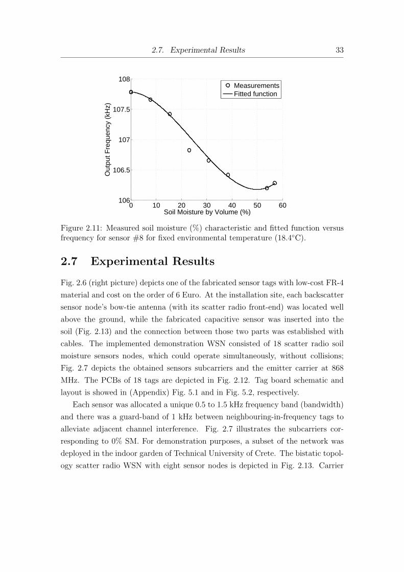
in Fig. 2.11.
Fig. 2.11 shows an interesting saturation effect (at the output frequency), when

2.6. Calibration 32
20
30
40
50
0
20
40
60
104
105
106
107
108
109
Temperature (C)
Soil Moisture by Volume (%)
Ou
tpu
t F
req
ue
nc
y (
kH
z)
Figure 2.10: Measured soil moisture (%) characteristic and polynomially-fittedfunction versus frequency and temperature for sensor #8. The data measurementswere 226 sets of soil moisture, temperature and output frequency samples.
the soil moisture by volume reaches 48%. That is due to the hydraulic properties
of all soil textures. Specifically, “total pore space, expressed on a volumetric basis,
ranges from 40% in sandy soil to 48% in clay soil. When a soil is completely
saturated, all the pores are filled with water. Thus, porosity is also the water
content at saturation, expressed as the volume of water per volume of soil.” [44,
chapter 6 ”Soils”, p. 167]. Thus, the observed saturation above 48% of the sensor
is clearly coherent with the physical phenomenon of water content in various soil
textures and thus, an indirect indication that the sensor is working properly.
Measured %SM results using the above procedure of (2.23), (2.24) were com-
pared with the sensor’s output; for data of Fig. 2.11 (fixed temperature), root
mean squared error (RMSE) of 0.15% SM and mean absolute error (MAE) of
0.13% SM were found. Such error will be denoted as calibration error, since it
does not include the error due to scatter radio communication, studied below.
2.7. Experimental Results 33
0 10 20 30 40 50 60106
106.5
107
107.5
108
Soil Moisture by Volume (%)
Out
put F
requ
ency
(kH
z)
MeasurementsFitted function
Figure 2.11: Measured soil moisture (%) characteristic and fitted function versusfrequency for sensor #8 for fixed environmental temperature (18.4C).
2.7 Experimental Results
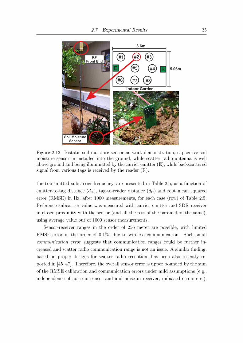
Fig. 2.6 (right picture) depicts one of the fabricated sensor tags with low-cost FR-4
material and cost on the order of 6 Euro. At the installation site, each backscatter
sensor node’s bow-tie antenna (with its scatter radio front-end) was located well
above the ground, while the fabricated capacitive sensor was inserted into the
soil (Fig. 2.13) and the connection between those two parts was established with
cables. The implemented demonstration WSN consisted of 18 scatter radio soil
moisture sensors nodes, which could operate simultaneously, without collisions;
Fig. 2.7 depicts the obtained sensors subcarriers and the emitter carrier at 868
MHz. The PCBs of 18 tags are depicted in Fig. 2.12. Tag board schematic and
layout is showed in (Appendix) Fig. 5.1 and in Fig. 5.2, respectively.
Each sensor was allocated a unique 0.5 to 1.5 kHz frequency band (bandwidth)
and there was a guard-band of 1 kHz between neighbouring-in-frequency tags to
alleviate adjacent channel interference. Fig. 2.7 illustrates the subcarriers cor-
responding to 0% SM. For demonstration purposes, a subset of the network was
deployed in the indoor garden of Technical University of Crete. The bistatic topol-
ogy scatter radio WSN with eight sensor nodes is depicted in Fig. 2.13. Carrier

2.7. Experimental Results 34
Figure 2.12: 18 Soil Moiture Sensor Tag Designs.
emitter (E) and RTL-SDR reader (R) were located at either sides of the field with
the sensors in between. Capacitive sensors were inserted into the soil near the root
of each plant, while the scatter radio front-ends were placed 1.5 meter above the
ground, using canes.
Sampled data time series collected from approximately seven hours of continu-
ous monitoring are illustrated in Fig. 2.14. It can be easily observed that after the
watering instances, the output frequency of the sensors changed instantly, while it
settled after a limited amount of time.
In order to achieve both communication performance characterization and sens-
ing accuracy of the proposed WSN, maximum communication range and end-
to-end sensing accuracy were experimentally measured. Specifically, a complete
bistatic topology link was utilized outdoors (Fig. 2.15).
Carrier emitter, SDR receiver and sensor/tag (with subcarrier center frequency
at 109 kHz) were installed at 1.3 m height. Temperature of 18C was measured,
soil moisture was fixed at 0% SM (corresponding to 109 kHz subcarrier frequency
for the specific sensor), sampling rate was set to 1 MHz and duration of 100 ms
was exploited per sensor measurement. Communication performance was tested for
various installation topologies and the corresponding results, in terms of estimating
2.7. Experimental Results 35
Indoor ardenG
#1
E R
#2
#5
#3
#4
#8#7#6
Soil MoistureSensor
RFFront End
5.06m
8.6m
Figure 2.13: Bistatic soil moisture sensor network demonstration; capacitive soilmoisture sensor in installed into the ground, while scatter radio antenna is wellabove ground and being illuminated by the carrier emitter (E), while backscatteredsignal from various tags is received by the reader (R).
the transmitted subcarrier frequency, are presented in Table 2.5, as a function of
emitter-to-tag distance (det), tag-to-reader distance (dtr) and root mean squared
error (RMSE) in Hz, after 1000 measurements, for each case (row) of Table 2.5.
Reference subcarrier value was measured with carrier emitter and SDR receiver
in closed proximity with the sensor (and all the rest of the parameters the same),
using average value out of 1000 sensor measurements.
Sensor-receiver ranges in the order of 256 meter are possible, with limited
RMSE error in the order of 0.1%, due to wireless communication. Such small
communication error suggests that communication ranges could be further in-
creased and scatter radio communication range is not an issue. A similar finding,
based on proper designs for scatter radio reception, has been also recently re-
ported in [45–47]. Therefore, the overall sensor error is upper bounded by the sum
of the RMSE calibration and communication errors under mild assumptions (e.g.,
independence of noise in sensor and and noise in receiver, unbiased errors etc.),

2.7. Experimental Results 36
Figure 2.14: Simultaneous and continuous soil moisture sensing from 8 tags, as afunction of time, using the proposed scatter radio sensor network.
which for the above values of Table 2.5 and the results of Section 2.6 offers overall
RMSE below 1% SM. Finally, it is noted that for all experimental results, emitter
transmission power was 13 dBm at 868 MHz.

2.7. Experimental Results 37
d =256 mtr
Carrier Emitter
RTL SDR Reader
Tag
d =3 met
Figure 2.15: Testing outdoors the communication range of the specific bistaticanalog backscatter architecture.
Table 2.5: Communication Accuracy.
# det (m) dtr (m) RMSE (Hz) RMSE (%)
1 3 48.3 12.91 0.011
2 3 69 17.00 0.015
3 3 146 26.89 0.024
4 3 205 31.39 0.028
5 3 256 35.28 0.032
6 8.4 60.8 21.41 0.019
7 8.4 138 32.63 0.029
8 21.4 126 9.70 0.008

38
Chapter 3
Dual Band RF Harvesting &
Low-Power Supply System
Nowadays an ocean of electromagnetic waves surrounds us, most of that ambient
electromagnetic energy remains unused. Globally, the number of radio frequency
(RF) emitters has been continuously increasing, due to widespread use of wireless
technologies, such as cellular networks, Wi-Fi, digital TV and wireless sensor net-
works (WSN). Collection of ambient RF energy and its use of powering electrical
devices is an engineering challenge [48]. Over the last years, wireless power trans-
fer (WPT) based on far-field electromagnetic radiation is recommended for large
amount of sensors due to their necessity to be autonomous and self-sustained in
power [11], while battery replacement is a lengthy and costly procedure in large
sensor networks. This WPT concept is suitable for Internet of Things (IoT) ap-
plications such as environmental WSNs and sensor networks for smart cities. The
collection of unused ambient RF energy with rectifiers and supply of backscatter
radio WSNs (sensors of first part of this work) [21], [32] for example, is a great
engineering challenge. In this work, FM and VHF-UHF carrier emitters (e.g., in
bistatic scatter radio sensor networks [45], [46]) will be considered as potential RF
power sources. On the other hand, ambient RF energy harvesting offers a rela-
250 nH120 pF18 nH
3.3 pF
470 nH 22 nF 82 pF
10000 pF
SMS7630-040LF
SMS7630-040LF
Pin
Vin Iin Pout
VoutRL8.2 kΩ
+
-
+
-
Figure 3.1: The double diode rectifier design.
tively low energy density of some uW/cm2, compared to other power sources (e.g.
3.1. Rectifier 39
solar energy or energy from soil [49]), however it can operate in hybrid mode, in
conjunction with multiple other sources [16]. Efficiency is an important parame-
ter in a rectifier topology, i.e. the ratio of DC output power to RF input power.
Nowadays, significant research effort has been directed towards high-efficiency rec-
tifiers. Many attempts emphasize on the required impedance matching circuit
inductances, while minimizing reflection coefficient. For example, RF-to-DC recti-
fication efficiency of 20.5% and 35.3% was attained in [15] for −20 dBm and −10
dBm input power, respectively.
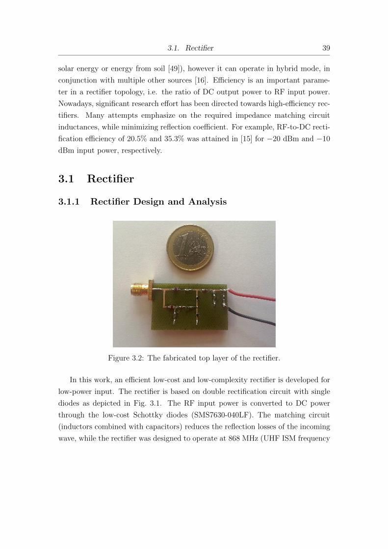
3.1 Rectifier
3.1.1 Rectifier Design and Analysis
Figure 3.2: The fabricated top layer of the rectifier.
In this work, an efficient low-cost and low-complexity rectifier is developed for
low-power input. The rectifier is based on double rectification circuit with single
diodes as depicted in Fig. 3.1. The RF input power is converted to DC power
through the low-cost Schottky diodes (SMS7630-040LF). The matching circuit
(inductors combined with capacitors) reduces the reflection losses of the incoming
wave, while the rectifier was designed to operate at 868 MHz (UHF ISM frequency

3.1. Rectifier 40
0 200 400 600 800 1000−30
−25
−20
−15
−10
−5
0
Frequency (MHz)
S11
(dB
)
MeasurementSimulation
Figure 3.3: Reflection coefficient at the input of rectifier.
in Europe) and at 97.5 MHz (center of FM band), simultaneously. Harmonic-
balance and Momentum solver was employed for simulations. The FR-4 substrate
was modelled with εr = 4.4, tan δ = 0.025, copper thickness 35 µm and substrate
height 1.6 mm. The first goal of modelling and simulation was the maximization
of the RF to DC efficiency:
η =Pout
Pin
=V 2out/RL
Pin
, (3.1)
with Pin, Pout the input and output power and Vout the voltage across the load RL.
The second goal was the minimization of reflection coefficient,
Γin =Zin − 50
Zin + 50, (3.2)
for input power Pin −20 dBm at 868 MHz and 97.5 MHz. The input impedance
Zin is defined as (Fig. 3.1):
Zin =VinIin
. (3.3)
After optimization, the dual-band prototype was implemented with discrete
components and fixed trace dimensions, as shown in Fig. 3.2. The load at the
3.1. Rectifier 41
-30 -25 -20 -15 -10 -50
10
20
30
40
50
Power Input (dBm)
Effi
cie
ncy (
%)
Measurement
Simulation
868 MHz
1 .494 %
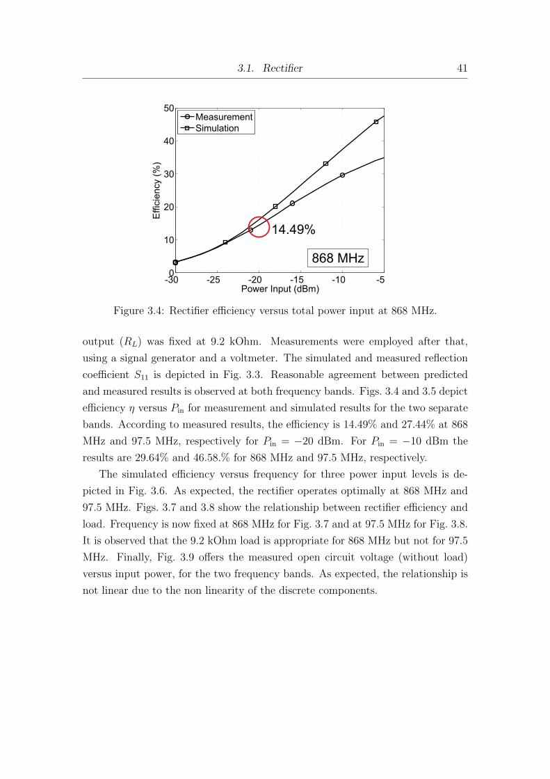
Figure 3.4: Rectifier efficiency versus total power input at 868 MHz.
output (RL) was fixed at 9.2 kOhm. Measurements were employed after that,
using a signal generator and a voltmeter. The simulated and measured reflection
coefficient S11 is depicted in Fig. 3.3. Reasonable agreement between predicted
and measured results is observed at both frequency bands. Figs. 3.4 and 3.5 depict
efficiency η versus Pin for measurement and simulated results for the two separate
bands. According to measured results, the efficiency is 14.49% and 27.44% at 868
MHz and 97.5 MHz, respectively for Pin = −20 dBm. For Pin = −10 dBm the
results are 29.64% and 46.58.% for 868 MHz and 97.5 MHz, respectively.
The simulated efficiency versus frequency for three power input levels is de-
picted in Fig. 3.6. As expected, the rectifier operates optimally at 868 MHz and
97.5 MHz. Figs. 3.7 and 3.8 show the relationship between rectifier efficiency and
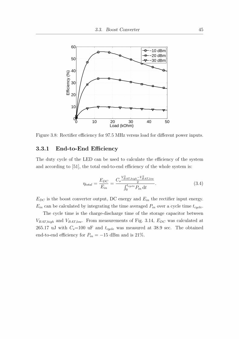
load. Frequency is now fixed at 868 MHz for Fig. 3.7 and at 97.5 MHz for Fig. 3.8.
It is observed that the 9.2 kOhm load is appropriate for 868 MHz but not for 97.5
MHz. Finally, Fig. 3.9 offers the measured open circuit voltage (without load)
versus input power, for the two frequency bands. As expected, the relationship is
not linear due to the non linearity of the discrete components.
3.2. Antenna Design 42
-30 -25 -20 -15 -10 -50
10
20
30
40
50
60
Power Input (dBm)
Effi
cie
ncy (
%)
Measurement
Simulation
97.5 MHz
27.44%
Figure 3.5: Rectifier efficiency versus total power input at 97.5 MHz.
3.2 Antenna Design
In order to supply the rectifier with wirelessly harvested power, a microstrip
multi-band antenna was designed and fabricated. Specifically, a hybrid microstrip
monopole antenna was designed to operate at ISM band (around 868 MHz) and
at FM band (around 100 MHz). The design is a variation of a monopole antenna
(of wide-band operation) with a loop for FM band resonance (and low fabrication
complexity) on FR-4 substrate. The fabricated antenna is depicted in Fig. 3.10
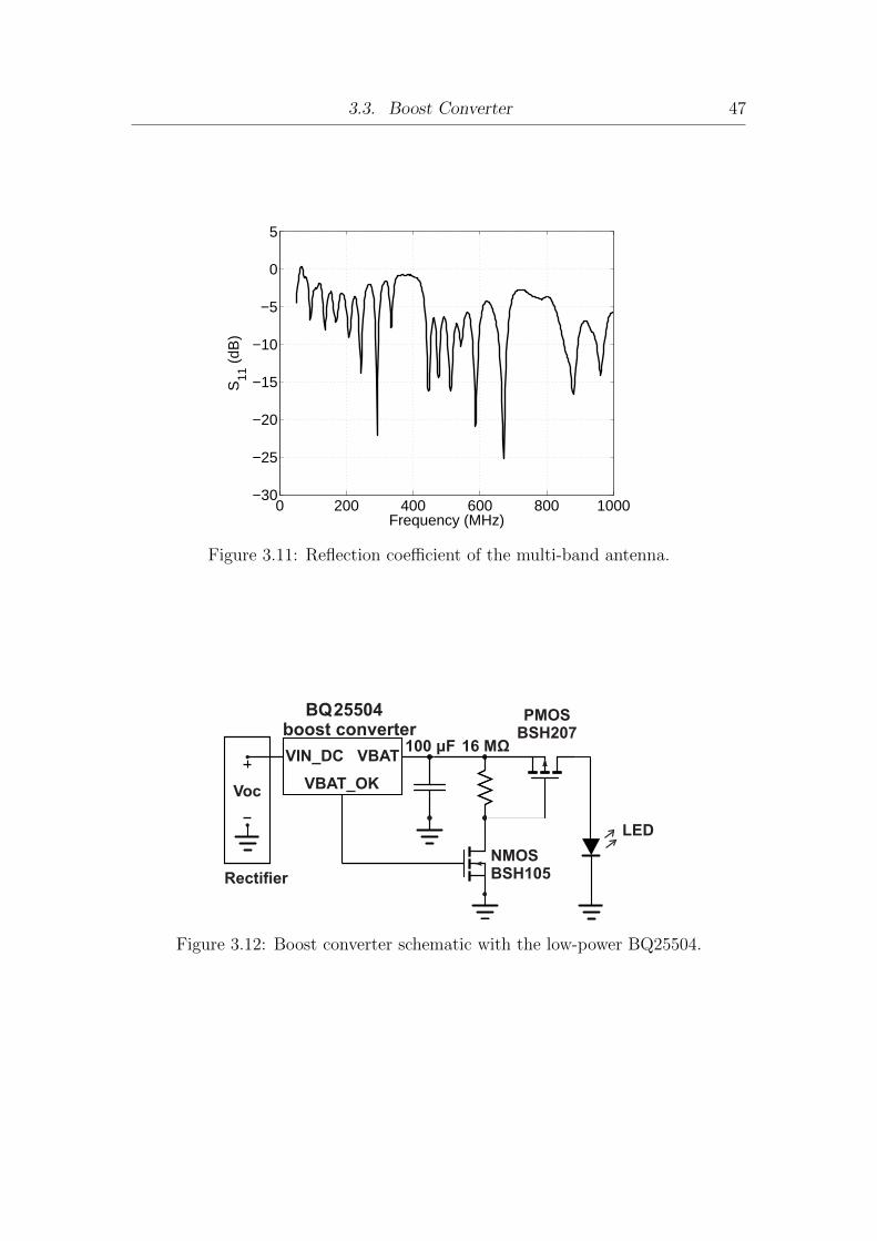
and its measured reflection coefficient is depicted in Fig. 3.11.
3.3 Boost Converter
In this work, the low-power boost converter Texas Instrument “bq25504” was uti-
lized [50]. The latter is an integrated-circuit with maximum power point tracking
(MPPT), minimum cold start voltage and typical input power of 330 mV and 10
µW, respectively, and low quiescent current (≤ 330 nA). Hence, for minimum volt-
age of 330 mV and typical power of 10 µW, the boost converter input impedance
is 10890 Ohm, which is close to 9200 Ohm (i.e. the load value for optimum RF

3.3. Boost Converter 43
0 200 400 600 800 10000
10
20
30
40
50
60
Frequency (MHz)
Effi
cien
cy (
%)
−10 dBm−20 dBm−30 dBm
Figure 3.6: Rectifier efficiency versus frequency for different power inputs.
to DC efficiency of the proposed rectifier). However, due to the MPPT function
(which aims to extract the maximum power from the rectifier output), as well
as the fact that the boost converter has two main operational modes (one for
cold-start operation and one after cold-start, with main boost charger enabled),
the input impedance does not remain constant. The MPPT functionality includes
periodic sampling of the input (open) voltage signal, after disabling the charger
for a limited duration of time (on the order of 256 ms every 16 sec); the cold
start charger is an unregulated, hysteretic boost converter with lower efficiency
compared to the main boost charger and provides the initial power so that the
latter can start its operation. This work measured experimentally the end-to-end
input-output relationship of the whole system, as described below.
The rectifier was designed to connected to the analog backscatter sensor node
through the “bq25504”. Fig. 3.12 depicts the circuit schematic topology. Rectifier
voltage (Voc ≡ VIN DC) was boosted (VBAT) and a 100 µF capacitor was charged
from 0 V. It is noted that the boost converter was self-started (cold start) and
no external energy was used. Digital signal output (VBAT OK) is set to high and
low, when the capacitor voltage reaches a pre-defined upper and lower limit, re-
spectively. In this work, the boost converter was designed to have low and upper

3.3. Boost Converter 44
0 10 20 30 40 500
5
10
15
20
25
30
35
40
Load (kOhm)
Effi
cien
cy (
%)
−10 dBm−20 dBm−30 dBm
Figure 3.7: Rectifier efficiency for 868 MHz versus load for different power inputs.
voltage threshold 2.4 V and 2.8 V, respectively.
An external PMOS (“BSH207”) was placed between the output load (in our
case is a LED, for future work will be a scatter radio sensor node) and the VBAT
pin. The inverted VBAT OK signal (through the open drain NMOS “BSH105”) was
used to drive the gate of the PMOS. While VBAT is lower than 2.8 V, PMOS
stays off (zero current) and the boost converter charges the capacitor. Next, when
the VBAT reaches 2.8 V, PMOS turns on and energy flows from the capacitor to
the LED. Next, capacitor is discharged and when VBAT = 2.4 V, PMOS turns
off again and current stops flowing to the LED. Then, the capacitor is charged
again until VBAT = 2.8 V and the procedure is repeated. A data acquisition (DAQ
NI USB-6356) instrument was used in order to measure the voltage across the
rectifier output (VIN DC) and the capacitor (VBAT). The measurement setup is
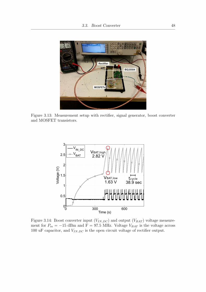
depicted in Fig. 3.13 and charge-discharge operation of the LED can be observed
in Fig. 3.14 for 800 seconds duration. The rectifier Pin was −15 dBm at 97.5 MHz.
Finally, it is noted again that the boost converter was self-started and no external
energy was used. The boost converter with the MOSFET switches was designed
and constructed in one PCB as is depicted in Fig. 5.3 (board schematic), Fig. 5.4
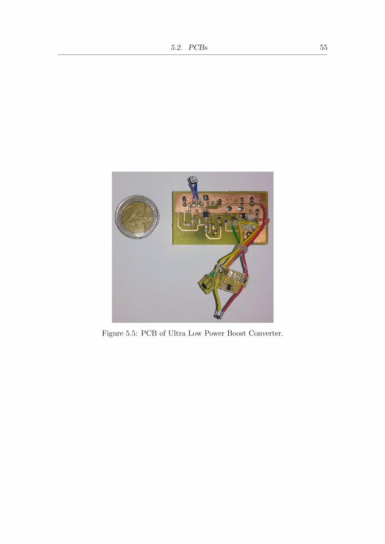
(board layout) and Fig. 5.5 (PCB).
3.3. Boost Converter 45
0 10 20 30 40 500
10
20
30
40
50
60
Load (kOhm)
Effi
cien
cy (
%)
−10 dBm−20 dBm−30 dBm
Figure 3.8: Rectifier efficiency for 97.5 MHz versus load for different power inputs.
3.3.1 End-to-End Efficiency
The duty cycle of the LED can be used to calculate the efficiency of the system
and according to [51], the total end-to-end efficiency of the whole system is:
ηtotal =EDC
Ein
=Cs
V 2BAT,high−V
2BAT,low
2∫ tcycle0
Pin dt. (3.4)
EDC is the boost converter output, DC energy and Ein the rectifier input energy.
Ein can be calculated by integrating the time averaged Pin over a cycle time tcycle.
The cycle time is the charge-discharge time of the storage capacitor between
VBAT,high and VBAT,low. From measurements of Fig. 3.14, EDC was calculated at
265.17 uJ with Cs=100 uF and tcycle was measured at 38.9 sec. The obtained
end-to-end efficiency for Pin = −15 dBm and is 21%.

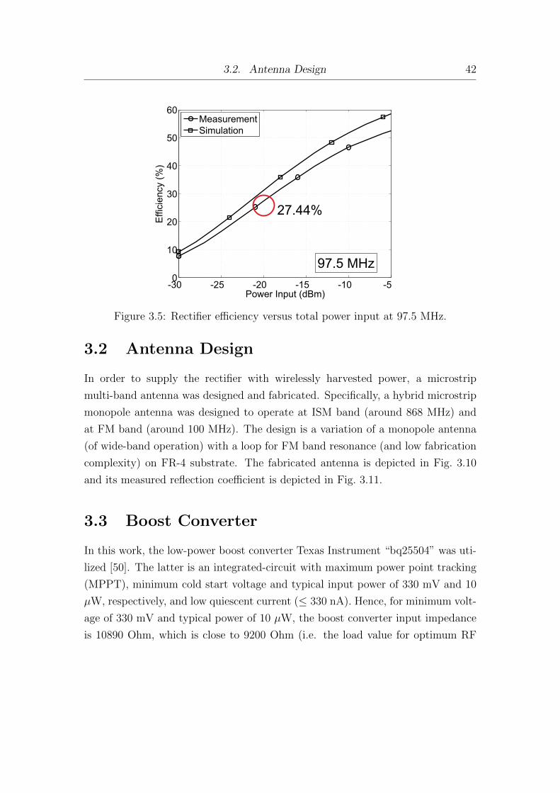
3.3. Boost Converter 46
−30 −25 −20 −15 −10 −5 00
1
2
3
4
5
Power Input (dBm)
Voc
(V
olts
)
868 MHz97.5 MHz
Figure 3.9: Measured rectifier output open circuit voltage for 97.5 MHz and 868MHz.
Figure 3.10: The fabricated multi-band antenna.
3.3. Boost Converter 47
0 200 400 600 800 1000−30
−25
−20
−15
−10
−5
0
5
Frequency (MHz)
S11
(dB
)
Figure 3.11: Reflection coefficient of the multi-band antenna.
25504boost converter
VIN_DC
VBAT_OK
VBAT100 Fμ 16 MΩ
NMOSBSH105
PMOSBSH207
Voc
LED
Rectifier
BQ
Figure 3.12: Boost converter schematic with the low-power BQ25504.
3.3. Boost Converter 48
MOSFETs
Rectifier
BQ25504
Figure 3.13: Measurement setup with rectifier, signal generator, boost converterand MOSFET transistors.
0 300 6000
0.5
1
1.5
2
2.5
3
Time (s)
Vo
lta
ge
(V
)
VIN_DC
VBAT
1.63 V
2.82 V
38.9 sec
VBAT,high
VBAT,low tcycle
Figure 3.14: Boost converter input (VIN DC) and output (VBAT ) voltage measure-ment for Pin = −15 dBm and F = 97.5 MHz. Voltage VBAT is the voltage across100 uF capacitor, and VIN DC is the open circuit voltage of rectifier output.
49
Chapter 4
Conclusions
4.1 Conclusion
The first part of the thesis describes in detail the development of an ultra-low
power and cost scatter radio network for soil moisture. Communication ranges
in the order of 250 meter were experimentally demonstrated, with overall RMSE,
less than 1%. Scaling issues were also discussed. The power consumption of each
scatter radio sensor is in the order of 200 µW.
The second part presents the design and implementation of a dual band RF
rectifier system with a commodity DC-DC converter. Its high efficiency and tested
operation at low-power input could perhaps enable the proposed WSN powered by
ambient RF. The circuit was designed with two single diodes, on a low-cost, lossy
FR-4 substrate. The system collects the RF energy from scatter radio emitters at
868 MHz and from one FM frequency at 97.5 MHz. Also a multi-band antenna
was designed and constructed. Experimental results with a commodity DC-DC
converter from cold-start were also presented and discussed.
4.2 Future Work
Future work should be focused towards the development of a full FM band rectifier.
The energy harvesting system will exploit all FM band frequencies and scatter
radio emitters frequency in order to capture much more unused energy. Future
efforts should aim to combine the capabilities of the two developed systems in order
to design a battery-less scatter radio sensor having the FM band and emitters as
a power source. Finally, an ultra large scale network of such sensor nodes should
be exploited, with ultra low cost sensor nodes having capacitors as energy tanks.

50
Chapter 5
Appendix
5.1 Matlab Receiver Code
1 %E l e u t h e r i o s Kabianakis
2 %Spyridon−Nektar ios Daska lak i s
3 c l o s e a l l ;
4 c l e a r a l l ;
5 c l c ;
6
7 Fs = 250 e3 ; % same as gnuradio
8 Ts = 1/Fs ;
9
10 Reso lut ion = 1 ; % in Hz
11 N F = Fs/ Reso lut ion ;
12 F ax i s = −Fs /2 : Fs/N F : Fs/2−Fs/N F ;
13
14 %Subca r r i e r c en te r Freq in Hz
15 SUB CENTER = [ 1 0 9 0 0 0 ] ;
16 %Sensors bandwidth
17 SUB BW = 1.5 e3 ;
18
19 %read samples from a f i f o
20 f i = fopen ( ’ RTL SDR fifo ’ , ’ rb ’ ) ;
21
22 t sampl ing = 1 ; % seconds
23 N samples = round ( Fs* t sampl ing ) ;
24 t = 0 : Ts : t sampl ing−Ts ;
25

5.1. Matlab Receiver Code 51
26 counter = 0 ;
27 packets = 0 ;
28 p lo t1 =1;
29
30 HIST SIZE = 1000 ; %stop a f t e r 1000 i r e r a t i o n s
31 F s e n s e h i s t = ze ro s ( HIST SIZE , 1 ) ;
32 h i s t s = 0 ;
33
34 whi le (1 )
35 x = f r ead ( f i , 2*N samples , ’ f l o a t 3 2 ’ ) ; % get samples
(*2 f o r I−Q)
36 x = x ( 1 : 2 : end ) + j *x ( 2 : 2 : end ) ; %
d e i n t e r l e a v i n g
37 counter = counter + 1 ;
38
39 i f mod( counter , 2) == 0
40 packets = packets + 1 ;
41 % f f t
42 x f f t = f f t s h i f t ( f f t (x , N F) ) ;
43 % cfo es t imate
44 [ mval mpos ] = max( abs ( x f f t ) ) ;
45 DF est = F ax i s (mpos ) ;
46 % cfo c o r r e c t i o n
47 x c o r r = x .* exp(− j *2* pi *DF est* t ) . ’ ;
48 % c o r r e c t e d c f o
49 x c o r r f f t = f f t s h i f t ( f f t ( x cor r , N F) ) ;
50
51 % sensor ’ s f f t
52 LEFT = SUB CENTER − SUB BW;
53 RIGHT = SUB CENTER + SUB BW;
54 x s e n s o r f f t = x c o r r f f t ;
55 x s e n s o r f f t ( F ax i s < −RIGHT) = 0 ;
56 x s e n s o r f f t ( F ax i s > RIGHT) = 0 ;
5.1. Matlab Receiver Code 52
57 x s e n s o r f f t ( abs ( F ax i s ) < LEFT) = 0 ;
58
59 %f i n d s u b c a r r i e r
60 [ mval mpos ] = max( abs ( x s e n s o r f f t ) ) ;
61 F s e n s o r e s t = abs ( F ax i s (mpos ) ) ;
62 mval2=10* l og10 ( ( abs ( mval ) . ˆ 2 ) *Ts) ;
63 F sensor power = mval2 ;
64 f p r i n t f ( ’N=%d |F=%5.1 f |Power=%7.1 f \n ’ , packets ,
F s en so r e s t , F sensor power )
65 F s e n s e h i s t ( packets ) = F s e n s o r e s t ;
66
67 i f p l o t1 ==1;
68 % plo t
69 f i g u r e (1 ) ;
70 subplot (2 , 1 , 1) ;
71 p lo t ( t , r e a l ( x c o r r ) ) ;
72 hold on ;
73 p lo t ( t , imag ( x c o r r ) , ’ g−− ’ ) ;
74 hold o f f ;
75 drawnow ;
76 subplot (2 , 1 , 2) ;
77 semi logy ( F axis , ( abs ( x c o r r f f t ) . ˆ 2 ) ) ;
78 g r id on ;
79 a x i s t i g h t ;
80 drawnow ;
81 end
82 i f (mod( packets , HIST SIZE ) == 0)
83 r e turn ;
84 end
85 end
86 end
5.2. PCBs 53
5.2 PCBs
Figure 5.1: Schematic of the tag.
Figure 5.2: Tag PCB layout.
5.2. PCBs 54
Figure 5.3: Schematic of the Ultra Low Power Boost Converter with CapasitorManagement.
Figure 5.4: PCB layout of Ultra Low Power Boost Converter.
5.2. PCBs 55
Figure 5.5: PCB of Ultra Low Power Boost Converter.
56
Bibliography
[1] G. Vellidis, V. Garrick, S. Pocknee, C. Perry, C. Kvien, and M. Tucker, “How
wireless will change agriculture,” Precision agriculture, vol. 7, pp. 57–68, 2007.
[2] M. Haefke, S. Mukhopadhyay, and H. Ewald, “A Zigbee based smart sensing
platform for monitoring environmental parameters,” in Proc. IEEE Int. Conf.
on Instrum. and Meas. Techn. (I2MTC), Binjiang, China, May. 2011, pp. 1–8.
[3] G. R. Mendez, M. A. M. Yunus, and S. C. Mukhopadhyay, “A WiFi based
smart wireless sensor network for monitoring an agricultural environment,”
in Proc. IEEE Int. Conf. on Instrum. and Meas. Techn. (I2MTC), Graz,
Austria, May. 2012, pp. 2640–2645.
[4] D. Antolın, A. Bayo, N. Medrano, B. Calvo, and S. Celma, “Wubinet: A
flexible WSN for applications in environmental monitoring,” in Proc. IEEE
Int. Conf. on Instrum. and Meas. Techn. (I2MTC), Graz, Austria, May. 2012,
pp. 2608–2611.
[5] V. Palazzari, P. Mezzanotte, F. Alimenti, F. Fratini, G. Orecchini, M. Virili,
C. Mariotti, and L. Roselli, “Leaf compatible ”eco-friendly” temperature sen-
sor clip for high density monitoring wireless networks,” in Proc. IEEE 15th
Medit. Microw. Symp. (MMS), Lecce, Italy, Dec. 2015, pp. 1–4.
[6] Y. Kawahara, H. Lee, and M. M. Tentzeris, “Sensprout: inkjet-printed soil
moisture and leaf wetness sensor,” in Proc. ACM Conf. on Ubiquitous Com-
puting, Pittsburgh PA, USA, Sep. 2012, pp. 545–545.
[7] S. Sulaiman, A. Manut, and A. Nur Firdaus, “Design, fabrication and testing
of fringing electric field soil moisture sensor for wireless precision agriculture
applications,” in Proc. IEEE Int. Conf. on Inf. and Multim. Techn. (ICIMT),
Jeju Island, South Korea, Sep. 2009, pp. 513–516.
Bibliography 57
[8] S. Kim, Y. Kawahara, A. Georgiadis, A. Collado, and M. Tentzeris, “Low-cost
inkjet-printed fully passive RFID tags using metamaterial-inspired antennas
for capacitive sensing applications,” in Proc. IEEE Int. Microw. Symp. (IMS),
Seattle WA, USA, Jun. 2013, pp. 1–4.
[9] Y. Liu, Y. He, M. Li, J. Wang, K. Liu, L. Mo, W. Dong, Z. Yang, M. Xi,
J. Zhao, and X.-Y. Li, “Does wireless sensor network scale? A measurement
study on GreenOrbs,” in Proc. IEEE INFOCOM, Shanghai, China, Apr. 2011,
pp. 873–881.
[10] G. Vannucci, A. Bletsas, and D. Leigh, “A software-defined radio system for
backscatter sensor networks,” IEEE Trans. Wireless Commun., vol. 7, no. 6,
pp. 2170–2179, Jun. 2008.
[11] S. Kim, C. Mariotti, F. Alimenti, P. Mezzanotte, A. Georgiadis, A. Col-
lado, L. Roselli, and M. M. Tentzeris, “No battery required: perpetual RFID-
enabled wireless sensors for cognitive intelligence applications,” IEEE Microw.
Mag., vol. 14, no. 5, pp. 66–77, Jul. 2013.
[12] S. D. Assimonis, S.-N. Daskalakis, and A. Bletsas, “Sensitive and efficient RF
harvesting supply for batteryless backscatter sensor networks,” IEEE Trans.
Microw. Theory Techn., vol. 64, no. 4, pp. 1327–1338, Apr. 2016.
[13] J. Kimionis and M. M. Tentzeris, “RF tag front-end design for uncompromised
communication and harvesting,” in Proc. IEEE Conf. on RFID Techn. and
Appl. (RFID-TA), Tampere, Finland, Sep. 2014, pp. 109–114.
[14] S. D. Assimonis and A. Bletsas, “Energy harvesting with a low-cost and high
efficiency rectenna for low-power input,” in Proc. IEEE Radio and Wireless
Symp. (RWS), Newport Beach CA, USA, Jan. 2014, pp. 229–231.
[15] S. D. Assimonis, S.-N. Daskalakis, and A. Bletsas, “Efficient RF harvesting
for low-power input with low-cost lossy substrate rectenna grid,” in Proc.
IEEE Conf. on RFID Techn. and Appl. (RFID-TA), Tampere, Finland, Sep.
2014, pp. 1–6.
Bibliography 58
[16] K. Niotaki, F. Giuppi, A. Georgiadis, and A. Collado, “Solar/EM energy har-
vester for autonomous operation of a monitoring sensor platform,” Wireless
Power Transfer, vol. 1, no. 01, pp. 44–50, Mar. 2014.
[17] S. Caizzone, E. Digiampaolo, and G. Marrocco, “Investigation of suitable pa-
rameters for setup-independent RFID sensing,” in Proc. IEEE Int. EURASIP
Workshop on RFID Techn. (EURFID), Rosenheim, Germany, Oct. 2015, pp.
98–102.
[18] C. Occhiuzzi, C. Paggi, and G. Marrocco, “Passive RFID strain-sensor based
on meander-line antennas,” IEEE Antennas Propagat. Mag., vol. 59, no. 12,
pp. 4836–4840, Dec. 2011.
[19] R. Nair, E. Perret, S. Tedjini, and T. Barron, “A humidity sensor for passive
chipless RFID applications,” in Proc. IEEE Conf. on RFID Techn. and Appl.
(RFID-TA), Nice, France, Sep. 2012, pp. 29–33.
[20] R. Nair, E. Perret, and S. Tedjini, “Chipless RFID based on group delay en-
coding,” in Proc. IEEE Conf. on RFID Techn. and Appl. (RFID-TA), Sitges,
Spain, Sep. 2011, pp. 214–218.
[21] S.-N. Daskalakis, S. D. Assimonis, E. Kampianakis, and A. Bletsas, “Soil
moisture wireless sensing with analog scatter radio, low power, ultra-low cost
and extended communication ranges,” in Proc. IEEE Sensors Conf., Valencia,
Spain, Nov. 2014, pp. 122–125.
[22] A. Bletsas, S. Siachalou, and J. Sahalos, “Anti-collision tags for backscatter
sensor networks,” in Proc. IEEE 38th Europ. Microw. Conf. (EuMC), Ams-
terdam, Netherlands, Oct. 2008, pp. 179–182.
[23] H. Stockman, “Communication by means of reflected power,” Proc. IEEE
IRE, pp. 1196–1204, Oct. 1948.
[24] K. Kurokawa, “Power waves and the scattering matrix,” IEEE Trans. Microw.
Theory Techn., vol. 13, no. 2, pp. 194–202, Mar. 1965.

Bibliography 59
[25] P. V. Nikitin, K. S. Rao, S. F. Lam, V. Pillai, R. Martinez, and H. Heinrich,
“Power reflection coefficient analysis for complex impedances in RFID tag
design,” IEEE Trans. Microw. Theory Techn., vol. 53, no. 9, pp. 2721–2725,
Sep. 2005.
[26] J. D. Griffin and G. D. Durgin, “Complete link budgets for backscatter-radio
and RFID systems,” IEEE Antennas Propagat. Mag., vol. 51, no. 2, pp. 11–25,
Apr. 2009.
[27] A. Bletsas, A. G. Dimitriou, and J. N. Sahalos, “Improving backscatter radio
tag efficiency,” IEEE Trans. Microw. Theory Techn., vol. 58, no. 6, pp. 1502–
1509, Jun. 2010.
[28] S. D. Assimonis, E. Kampianakis, and A. Bletsas, “Microwave analysis and
experimentation for improved backscatter radio,” in Proc. IEEE Europ. Conf.
on Ant. and Prop. (EuCAP), Hague, Netherlands, Apr. 2014, pp. 3228–3229.
[29] S. Naderiparizi, A. N. Parks, Z. Kapetanovic, B. Ransford, and J. R. Smith,
“Wispcam: A battery-free RFID camera,” in Proc. IEEE Int. Conf. on RFID,
San Diego CA, USA, Apr. 2015.
[30] Y. Zhao and J. R. Smith, “A battery-free RFID-based indoor acoustic lo-
calization platform,” in Proc. IEEE Int. Conf. on RFID, Penang, Malaysia,
Apr.–May 2013, pp. 110–117.
[31] A. Dementyev and J. R. Smith, “A wearable UHF RFID-based EEG system,”
in Proc. IEEE Int. Conf. on RFID, Penang, Malaysia, Apr.–May 2013, pp.
1–7.
[32] E. Kampianakis, J. Kimionis, K. Tountas, C. Konstantopoulos, E. Koutroulis,
and A. Bletsas, “Wireless environmental sensor networking with analog scat-
ter radio and timer principles,” IEEE Sensors J., vol. 14, no. 10, pp. 3365–
3376, Oct. 2014.
[33] G. Vannucci, A. Bletsas, and D. Leigh, “Implementing backscatter radio for
wireless sensor networks,” in Proc. IEEE Int. Symp. on Person. Indoor and
Mob. Radio Commun., Athens, Greece, Sep. 2007, pp. 1–5.

Bibliography 60
[34] J. Kimionis, A. Bletsas, and J. N. Sahalos, “Bistatic backscatter radio for
tag read-range extension,” in Proc. IEEE Conf. on RFID Techn. and Appl.
(RFID-TA), Nice, France, Nov. 2012, pp. 356–361.
[35] “ERC Rep. 25 (2015).” [Online]. Available: http://www.erodocdb.dk/docs/
doc98/official/pdf/ERCRep025.pdf
[36] Custom Silicon Solutions (2009), CSS555 micropower timer, Product manual.
[Online]. Available: http://www.customsiliconsolutions.com/downloads/
Revised%20Standard%20products/CSS555 Spec.pdf
[37] S. W. Smith, The scientist and engineer’s guide to digital signal processing.,
California Technical Publishing, San Diego, 1997.
[38] Analog Devices (2005), ADG902 RF switch, Product manual. [Online].
Available: http://www.analog.com/media/en/technical-documentation/
data-sheets/ADG901 902.pdf
[39] Texas Instruments (2014), REF3318 voltage reference IC, Product manual.
[Online]. Available: http://www.ti.com/lit/ds/symlink/ref3318.pdf
[40] Perpetuum Inc. (2010), Free-Standing Vibration Energy Harvester. [Online].
Available: http://www.perpetuum.com/fsh.asp
[41] MicroPelt Inc. (2002), MPG-D651 Thermogenerator, Product manual.
[Online]. Available: http://thermalforce.de/engl/product/thermogenerator/
micropelt d751.pdf
[42] K. Pohlmann, Principles of Digital Audio (2nd Edition)., McGraw-Hill Com-
panies, Inc., 1989.
[43] P. Stoica and R. Moses, Spectral Analysis of Signals., Prentice-Hall Interna-
tional, Inc., 2005.
[44] G. B. Bonan, Ecological climatology: Concepts and Applications, (1st edi-
tion)., Cambridge Univ. Press, 2002.
[45] J. Kimionis, A. Bletsas, and J. N. Sahalos, “Increased range bistatic scatter
radio,” IEEE Trans. Commun., vol. 62, no. 3, pp. 1091–1104, Mar. 2014.
Bibliography 61
[46] N. Fasarakis-Hilliard, P. Alevizos, and A. Bletsas, “Coherent detection and
channel coding for bistatic scatter radio sensor networking,” IEEE Trans.
Commun., vol. 63, no. 5, pp. 1798–1810, May 2015.
[47] P. N. Alevizos and A. Bletsas, “Noncoherent composite hypothesis testing
receivers for extended range bistatic scatter radio WSNs,” in Proc. IEEE Int.
Conf. on Commun. (ICC), London, UK, Jun. 2015, pp. 4448–4453.
[48] S. Kim, R. Vyas, J. Bito, K. Niotaki, A. Collado, A. Georgiadis, and M. M.
Tentzeris, “Ambient RF energy-harvesting technologies for self-sustainable
standalone wireless sensor platforms,” Proc. IEEE, vol. 102, no. 11, pp. 1649–
1666, Nov. 2014.
[49] F. Lin, Y.-C. Kuo, J.-W. Hsieh, H.-Y. Tsai, Y. Liao, and H. Lee, “A self-
powering wireless environment monitoring system using soil energy,” IEEE
Sensors J., vol. 15, no. 7, pp. 3751–3758, Jul. 2015.
[50] Instruments, Texas (2011), BQ25504 Ultra Low Power Boost Converter
with Battery Management. [Online]. Available: http://www.ti.com/lit/ds/
symlink/bq25504.pdf
[51] M. Pinuela, P. D. Mitcheson, and S. Lucyszyn, “Ambient RF energy harvest-
ing in urban and semi-urban environments,” IEEE Trans. Microw. Theory
Techn., vol. 61, no. 7, pp. 2715–2726, Jul. 2013.