Embed Size (px)
Citation preview

General rights Copyright and moral rights for the publications made accessible in the public portal are retained by the authors and/or other copyright owners and it is a condition of accessing publications that users recognise and abide by the legal requirements associated with these rights.
Users may download and print one copy of any publication from the public portal for the purpose of private study or research.
You may not further distribute the material or use it for any profit-making activity or commercial gain
You may freely distribute the URL identifying the publication in the public portal If you believe that this document breaches copyright please contact us providing details, and we will remove access to the work immediately and investigate your claim.
Downloaded from orbit.dtu.dk on: Dec 17, 2021
Enhancement of the Purcell factor in multiperiodic hyperboliclike metamaterials
Chebykin, A. V.; Babicheva, V. E.; Iorsh, I. V.; Orlov, A. A.; Belov, P. A.; Zhukovsky, Sergei
Published in:Physical Review A
Link to article, DOI:10.1103/PhysRevA.93.033855
Publication date:2016
Document VersionPublisher's PDF, also known as Version of record
Link back to DTU Orbit
Citation (APA):Chebykin, A. V., Babicheva, V. E., Iorsh, I. V., Orlov, A. A., Belov, P. A., & Zhukovsky, S. (2016). Enhancementof the Purcell factor in multiperiodic hyperboliclike metamaterials. Physical Review A, 93(3), [033855].https://doi.org/10.1103/PhysRevA.93.033855

PHYSICAL REVIEW A 93, 033855 (2016)
Enhancement of the Purcell factor in multiperiodic hyperboliclike metamaterials
A. V. Chebykin,1 V. E. Babicheva,2,1 I. V. Iorsh,1 A. A. Orlov,1 P. A. Belov,1 and S. V. Zhukovsky1,3
1ITMO University, Kronverkskiy pr. 49, St. Petersburg 197101, Russia2Center for Nano-Optics, Georgia State University, P.O. Box 3965, Atlanta, Georgia 30302, USA
3DTU Fotonik, Department of Photonics Engineering, Technical University of Denmark, Ørsteds Plads 343, DK-2800 Kgs. Lyngby, Denmark(Received 23 June 2015; published 29 March 2016)
Spontaneous emission enhancement is theoretically investigated in multiperiodic metal-dielectric multilayers(multiperiodic hyperboliclike metamaterials or photonic hypercrystals) where the unit cell consists of two layersof different dielectrics alternating with identical metallic layers. It is shown that the Purcell factor in suchmultiperiodic structures exceeds the Purcell factor in ordinary periodic hyperbolic or plasmonic metamaterialsby a factor of 4, which in general makes it possible to maximize interaction between emitting centers and nearbyplasmonic structures. This enhancement is numerically characterized and shown to be related to the interplaybetween surface and volume plasmonic excitations in the multilayer metamaterial. We separately identify theinfluence of proximity between the emitter and the closest metal-dielectric boundary (including the quenchingeffect and the enhanced coupling of the dipole radiation and surface plasmon polaritons) and the effects related tothe structural composition of the hypercrystal. The Purcell-factor modification brought about by placing a cavitylayer into a multiperiodic structure was also characterized.
DOI: 10.1103/PhysRevA.93.033855
I. INTRODUCTION
Metamaterials, or artificially engineered nanocomposites,have become a very popular subject of research in the lastdecade, because these structures can provide electromagneticproperties that occur in natural materials rarely or not atall [1–3]. Within the concept of metamaterials one can realizenegative refraction [4,5], giant optical activity [6], anomalousbirefringence [7], ultrahigh Purcell-factor values [8,9], andoptical axis precession dependent on the wave vector [10]. Inparticular, interest in such structures has increased dramati-cally with the progress in the field of nanostructure fabrication(see review [11] for more details and references).
Metamaterial realization of indefinite media, which areextremely anisotropic media with permittivity tensor com-ponents having different signs, are especially interesting forseveral reasons. On the one hand, these realizations, alsocalled hyperbolic metamaterials (HMM) based on the factthat they feature hyperboloid-shaped isofrequency surfaces intheir dispersion relation [11–16], enable propagation of waveswith anomalously large wave vectors (arbitrarily large in theideal case). Such “high-k” waves, evanescent in conventionalmaterials but propagating in hyperbolic metamaterials, arespecial because their wavelengths, equal to 2π/k, can beextremely short, so these waves can constitute subwavelengthcarriers of information. This property is applied in the ideaof a hyperlens for image transmission with subwavelengthresolution in the far field [17]. In addition, the existenceof these high-k waves leads to an increase of the densityof photonic states in these structures, in turn leading toeffects such as strong and broadband spontaneous emissionenhancement [8,18,19], reduction of the surface plasmonlasing threshold [20], slow light [21,22], enhancement ofabsorption [23] and nonlinearity [24,25], and anomalous heattransfer beyond the Stefan-Boltzmann limit [26–28].
On the other hand, hyperbolic metamaterials can bepractically realized using relatively simple structures suchas an array of nanorods embedded in the substrate material[29–32] or a metal-dielectric multilayer [33–35]. Propagation
of high-k waves in the hyperbolic medium has been clearlyshown in [36,37]. As the characteristic size of the unitcell in hyperbolic metamaterials is much smaller than thewavelength of radiation in vacuum, one would expect that theycan be described using the effective medium model, wherethe electromagnetic response is determined by the averagedproperties of the composite rather than by the parametersof its individual elements, at least for wave vectors belowthe maximum values imposed by the finite size of the rodsand layers [9,18]. However, recent studies showed that theeffective medium approach in hyperbolic metamaterials breaksmuch sooner. The reason is that waves with large wave vectorspropagating in the metamaterial in question have a wavelengthmuch smaller than the wavelength in a vacuum, whichmodifies the limits of applicability of the effective mediummodel [38,39].
It was also shown that one can restore the validity of theeffective medium approach by introducing nonlocal effectivemedium parameters [40]. However, whether it is through thenonlocal effects [40,41] or through the photonic band-gapeffects [38], it turns out that the geometric structure of ametamaterial’s unit cell becomes very important in definingthe metamaterial’s optical properties. Therefore it becomespossible to control the propagation of high-k waves in hyper-bolic metamaterials by making the unit cell more complex. Forexample, in multilayer structures one can move from a simplemetal-dielectric bilayer to a unit cell containing more layers.Such a change affects the effective medium parameters onlyweakly, but the metamaterial properties are found to changedrastically. In a recent paper [42] we systematically studiedthe properties of such multiperiodic hyperbolic metamaterialswith unit cells containing more than one type of metal ordielectric [see Fig. 1(a)]. We showed that multiperiodicityprovides a way for engineering the metamaterial’s responsein the wave-vector space.
Such multiperiodic hyperbolic metamaterials can be re-garded as periodic metamaterials with an additional level ofstructuring, which have been recently introduced as multiscale
2469-9926/2016/93(3)/033855(9) 033855-1 ©2016 American Physical Society

A. V. CHEBYKIN et al. PHYSICAL REVIEW A 93, 033855 (2016)
(a) (b)
dAdmdB
,λp
,εA
,εB
Bcavity d ,εC...AMBMAMBMAMBMA... ...AMBMAMCMAMBMA...
εB
xy
z
FIG. 1. Geometry of structures under consideration. The unit cellconsists of four layers—two different dielectric (with thickness dA,dB
and dielectric permittivity εA,εB , denoted A and B, respectively)and two similar metallic (denoted M, with thickness dm and plasmawavelength λp = c/νp). (a) Regular structure formed by repeatingthe unit cell MAMB over N periods; (b) structure with the centrallayer having a different thickness dC �= dB forming a cavity layer C.
hyperbolic metamaterials [43] or, slightly later, photonichypercrystals [44,45]; the latter term suggests that a closerelationship to photonic crystals makes it possible to trans-fer the well-studied photonic band-gap effects in complexmultilayers [46] to plasmonic metamaterials. Specifically, itwas shown that changing the metamaterial topology fromperiodic to multiperiodic and introducing photonic-crystal–like features such as cavities [see Figs. 1(a) and 1(b)] can leadto unprecedented control both over bulk high-k waves [43]and over surface waves [45]. It was also shown that multi-layer structures support both resonant and nonresonant high-propagation wave vectors [47], and that resonant excitationsare accompanied by slow energy propagation, which bringsabout an additional increase of the Purcell factor [48].
These results suggest that even though multilayered hyper-bolic metamaterials have been rather well studied, there aremany questions left to be answered once we depart from thesimple alternating metal-dielectric stack in favor of a morecomplicated topology. One such question is the influence ofthe topology on the density of photonic states, and in turn,on spontaneous emission enhancement (Purcell factor) for anemitter embedded in a hyperbolic metamaterial. It was alreadydetermined that the Purcell enhancement can be very high for asimple metal-insulator-metal (MIM) structure with an ultrathingap layer [47,49–51]; such enhancement is expected to persistwhen ultrathin constituent layers are present in a metamaterialsetting. Moreover, the behavior of an emitter in a periodicmetamaterial shows a strong dependence on the exact positionof the emitter within a multilayer [9]. Therefore, studyingthe behavior of emitters in metamaterials with a complexmultilayer topology is likely to reveal interesting effects,similar to the known strong density of states modificationin photonic multilayers; this field has been a subject of avidresearch interest lately [1].
In this paper, we systematically characterize multiperiodichyperbolic metamaterial structures and determine the Purcellfactor for different placements of the emitter within them.Following the approach of [42], we focus on the biperiodicstructure with the unit cell consisting of four layers: twolayers of different dielectrics alternating with two similar
metallic layers. We show that the dipole radiation of the emitterprimarily couples to surface plasmon polaritons at the nearestmetal-dielectric boundaries. However, the enhancement of thePurcell effect pertaining to the global geometrical propertiesof the structure is demonstrated and is apparently relatedto the interplay between surface and volume plasmonicexcitations in the multilayer metamaterial. Hence, we showthat multiperiodicity not only leads to spectral redistribution ofthe Purcell factor, but also enhances the spontaneous emissionof an embedded dipole emitter beyond what is achievablein a regular periodic metal-dielectric structure. Therefore,increasing the complexity of the metamaterial topology isshown to be an alternative method of increasing the Purcellfactor complementary to the known effect of decreasing thedielectric layer thicknesses previously demonstrated in MIMstructures [52].
The paper is organized as follows. Section II is devotedto the description of the parameters of considered struc-tures, as well as the problem formulation. In Sec. III wepresent the investigation of the Purcell factor in biperiodichyperbolic metamaterials. We focus on the dependence ofthe Purcell factor on the permittivity of the dielectric layersin the structure, as well as on the emitter’s position withinthe dielectric layers. Section IV describes the behavior ofthe Purcell factor in biperiodic structures with a cavity layer.Finally, Sec. V summarizes the paper.
II. STRUCTURES AND METHODS
Following the approach in [42], we define multiperiodicstructures as metal-dielectric multilayers where the unit cellcontains more than one type of plasmonic interface. One meansto achieve this is to compose the unit cell of four layers denotedMBMA, where two layers made of a metal (denoted M, withthickness dm and permittivity εm(ω) varying according to theDrude model) alternate with two dielectric layers made ofdifferent dielectrics (denoted A and B with thicknesses dA,B
and permittivities εA,B), as shown in Fig. 1(a). The structure’seffective permittivity components can be determined using thestandard quasistatic homogenization (see [11] for details):
ε‖ = εAdA + εBdB + 2εm(ω)dm
dA + dB + 2dm
, (1)
1
ε⊥= ε−1
A dA + ε−1B dB + 2ε−1
m (ω)dm
dA + dB + 2dm
. (2)
If ε‖ and ε⊥ have different signs, we call such a structurea multiperiodic hyperbolic metamaterial. We note here thatthe term “hyperbolic” should be regarded only as a labelingterm, since the effective medium approximation as used inEqs. (1) and (2) is often inaccurate for complex plasmonicmultilayers [53]. Moreover, in many cases a metamaterialthat does not effectively have a hyperbolic dispersion (i.e.,for which the product ε‖ε⊥ has a positive real part) stillpossesses many of the features that were originally attributedto hyperbolic metamaterials, such as the existence of high-kplasmonic modes [9,39] and strong spontaneous emissionenhancement [54].
As opposed to the previous study [42] where consideringinfinite multiperiodic multilayers was necessary to determine
033855-2

ENHANCEMENT OF THE PURCELL FACTOR . . . PHYSICAL REVIEW A 93, 033855 (2016)
their dispersion relations, we calculate the Purcell factor infinite-sized multilayers in order to bring the problem closerto a possible experimental realization; such a structure withN periods can be symbolically represented as (MBMA)N . Inaddition to these structures, which we call regular since thereare no geometrical features in them except multiperiodicityitself, we consider modified structures created by introducinga cavity (or defect), or in other words, by replacing one of theMBMA periods by MCMA, where C denotes a cavity layerof thickness dC and permittivity εC = εB . The entire structurecan then be coded as (MBMA)M (MCMA)(MBMA)N−M−1.These structures are shown in Fig. 1(b).
Following the analysis in [43], we expect that the multiperi-odicity will introduce a photonic band gap for high-k waves,and adding a cavity layer will create a resonant state within thatband gap and localize the energy of a bulk plasmonic wave.The goal of the present investigation is to find out whether,and to what extent, this modification of the high-k wave-vectordomain will affect spontaneous emission enhancement for anemitter embedded in various locations in the structure.
In order to do so, we numerically calculate the Purcellfactor of an electric dipole emitter oriented along the y axisand placed in a certain point r0. The calculation is based on theinduced impedance numerical method [55], and in particular,on the relationship
f = Rin
R0in
= Im[Gyy(r0,r0,ω)]
Im[G0yy(r0,r0,ω)]
= Prad
P 0rad
, (3)
where Prad, Rin, and Gyy are, respectively, the radiated power,the input impedance of the dipole, and the Green’s functionin the presence of the structure, whereas P 0
rad, R0in, and G0
yy
are the same quantities in free space. Hence the Purcell factorf = Prad/P
0rad can be derived from the input impedance of the
dipole Rin, which is directly computed in the CST MICROWAVE
STUDIO package [55].This method was shown to be applicable to the Purcell-
factor calculation in a variety of frequency ranges, i.e., fromradio to optics [55,56]. More importantly, this method canbe applied to structures with complex geometry and finitedimensions, where analytic approaches do not work.
The structures under study contain N = 10 periods witheach layer measuring W = 700 nm in x and y directions.The layer thicknesses are dd = dA = dB = 37.5 nm and dm =25 nm. The permittivities of the dielectric layers εA and εB arevaried, and for the metal layers the Drude model is assumedwith equal to 83.4-THz collision frequency and varying plasmafrequency νp. A time-domain (transient) solver was used withthe accuracy setting varied between −30 and −40 dB to keepthe numerical errors below 5%. The boundary conditions areopen (perfectly matched layers), with added space betweenthe structure and the boundary. Additional symmetry planeswith respect to the electric and magnetic fields are includedto reduce the computational domain (electric symmetry onthe YZ plane and magnetic symmetry on the XZ plane).This way, a spatially finite structure in all directions issimulated. The lateral size of the structure W was confirmedto be sufficiently large that the dipole placed at x = y = 0is not sensitive to the exact values of W , so that the chosenstructure, while remaining practically relevant, enables direct
comparison to the previously obtained results for the spatiallyinfinite metamaterial.
III. PURCELL EFFECT IN REGULAR MULTIPERIODICSTRUCTURES
We first consider regular structures as shown in Fig. 1(a)and investigate the effect on the Purcell factor introduced bymultiperiodicity. The point emitter is placed in the middle ofthe central layer, which is of type B (see inset in Fig. 2).
We first keep the permittivity of the dielectric layers Aconstant (εA = 3.0) and vary the permittivity of dielectric inlayers B, in one of which the emitter is located. Namely, εB isset to vary from 1.8 to 4.6; the case εB = 3.0 = εA correspondsto the conventional periodic hyperbolic metamaterials inthe absence of multiperiodicity. The results are shown inFigs. 2(a) and 2(b). As one can see, even a minor degree ofmultiperiodicity (εB = 3.4) significantly modifies the Purcellfactor, introducing two enhancement regions compared to onlyone region for εB = 3.0. A further increase of εB results in theshift of both enhancement regions towards longer wavelengths,with the lower-frequency enhancement region shifting moreprominently, so that the gap between the two regions widens.Simultaneously, the peak value of the Purcell factor becomesmuch greater. Note that the Purcell-factor peak magnitudedoes not exhibit any marked preference with respect to εB
(where the emitter is placed), contrary to the expectation thatit would be higher for an emitter placed in an optically denserenvironment; for instance, the Purcell factors for εB = 2.2 andεB = 3.8 are approximately the same on Figs. 2(a) and 2(b).
The same dependence but for fixed εB = 4.6 and varyingεA from 3 to 5.8 is shown in Figs. 2(c) and 2(d); again,εA = 4.6 = εB is the case of absent multiperiodicity. Similarto the previous case, we observe that multiperiodicity leads
FIG. 2. Frequency dependence of the Purcell factor for the biperi-odic structure shown in Fig. 1(a) for different layer permittivities:(a, b) for constant εA = 3 and varying εB ; (c, d) for varying εA
and constant εB = 4.6. The point emitter is located in the middleof the central B layer (z = 0, see inset). The layer thicknesses aredA = dB = 37.5 nm and dm = 25 nm. Purcell factor is increased atfrequencies that correspond to plasmon excitations.
033855-3
A. V. CHEBYKIN et al. PHYSICAL REVIEW A 93, 033855 (2016)
( )
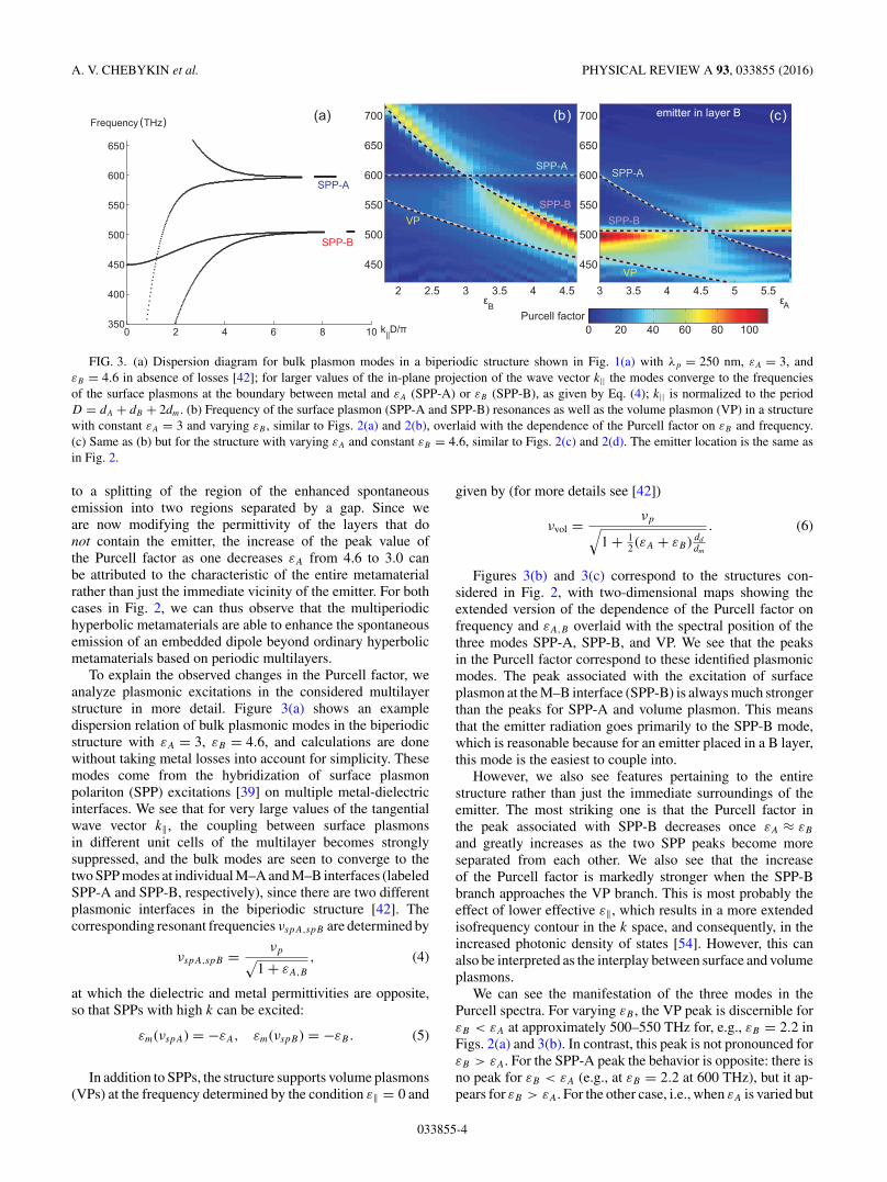
FIG. 3. (a) Dispersion diagram for bulk plasmon modes in a biperiodic structure shown in Fig. 1(a) with λp = 250 nm, εA = 3, andεB = 4.6 in absence of losses [42]; for larger values of the in-plane projection of the wave vector k|| the modes converge to the frequenciesof the surface plasmons at the boundary between metal and εA (SPP-A) or εB (SPP-B), as given by Eq. (4); k|| is normalized to the periodD = dA + dB + 2dm. (b) Frequency of the surface plasmon (SPP-A and SPP-B) resonances as well as the volume plasmon (VP) in a structurewith constant εA = 3 and varying εB , similar to Figs. 2(a) and 2(b), overlaid with the dependence of the Purcell factor on εB and frequency.(c) Same as (b) but for the structure with varying εA and constant εB = 4.6, similar to Figs. 2(c) and 2(d). The emitter location is the same asin Fig. 2.
to a splitting of the region of the enhanced spontaneousemission into two regions separated by a gap. Since weare now modifying the permittivity of the layers that donot contain the emitter, the increase of the peak value ofthe Purcell factor as one decreases εA from 4.6 to 3.0 canbe attributed to the characteristic of the entire metamaterialrather than just the immediate vicinity of the emitter. For bothcases in Fig. 2, we can thus observe that the multiperiodichyperbolic metamaterials are able to enhance the spontaneousemission of an embedded dipole beyond ordinary hyperbolicmetamaterials based on periodic multilayers.
To explain the observed changes in the Purcell factor, weanalyze plasmonic excitations in the considered multilayerstructure in more detail. Figure 3(a) shows an exampledispersion relation of bulk plasmonic modes in the biperiodicstructure with εA = 3, εB = 4.6, and calculations are donewithout taking metal losses into account for simplicity. Thesemodes come from the hybridization of surface plasmonpolariton (SPP) excitations [39] on multiple metal-dielectricinterfaces. We see that for very large values of the tangentialwave vector k‖, the coupling between surface plasmonsin different unit cells of the multilayer becomes stronglysuppressed, and the bulk modes are seen to converge to thetwo SPP modes at individual M–A and M–B interfaces (labeledSPP-A and SPP-B, respectively), since there are two differentplasmonic interfaces in the biperiodic structure [42]. Thecorresponding resonant frequencies νspA,spB are determined by
νspA,spB = νp√1 + εA,B
, (4)
at which the dielectric and metal permittivities are opposite,so that SPPs with high k can be excited:
εm(νspA) = −εA, εm(νspB) = −εB. (5)
In addition to SPPs, the structure supports volume plasmons(VPs) at the frequency determined by the condition ε‖ = 0 and
given by (for more details see [42])
νvol = νp√1 + 1
2 (εA + εB) dd
dm
. (6)
Figures 3(b) and 3(c) correspond to the structures con-sidered in Fig. 2, with two-dimensional maps showing theextended version of the dependence of the Purcell factor onfrequency and εA,B overlaid with the spectral position of thethree modes SPP-A, SPP-B, and VP. We see that the peaksin the Purcell factor correspond to these identified plasmonicmodes. The peak associated with the excitation of surfaceplasmon at the M–B interface (SPP-B) is always much strongerthan the peaks for SPP-A and volume plasmon. This meansthat the emitter radiation goes primarily to the SPP-B mode,which is reasonable because for an emitter placed in a B layer,this mode is the easiest to couple into.
However, we also see features pertaining to the entirestructure rather than just the immediate surroundings of theemitter. The most striking one is that the Purcell factor inthe peak associated with SPP-B decreases once εA ≈ εB
and greatly increases as the two SPP peaks become moreseparated from each other. We also see that the increaseof the Purcell factor is markedly stronger when the SPP-Bbranch approaches the VP branch. This is most probably theeffect of lower effective ε‖, which results in a more extendedisofrequency contour in the k space, and consequently, in theincreased photonic density of states [54]. However, this canalso be interpreted as the interplay between surface and volumeplasmons.
We can see the manifestation of the three modes in thePurcell spectra. For varying εB , the VP peak is discernible forεB < εA at approximately 500–550 THz for, e.g., εB = 2.2 inFigs. 2(a) and 3(b). In contrast, this peak is not pronounced forεB > εA. For the SPP-A peak the behavior is opposite: there isno peak for εB < εA (e.g., at εB = 2.2 at 600 THz), but it ap-pears for εB > εA. For the other case, i.e., when εA is varied but
033855-4

ENHANCEMENT OF THE PURCELL FACTOR . . . PHYSICAL REVIEW A 93, 033855 (2016)
( ) ( )
FIG. 4. Frequency dependence of the Purcell factor for a multilayer metamaterial structure [Fig. 1(a)] for different positions of point emitterin the central layer with εB = 4.6 and εA = 3 for different plasma frequencies of the metal layers: (a) λp = 250 nm and (b) λp = 226 nm. Thedistance din is the displacement of the emitter away from the center of the layer in which the emitter is placed (see insets).
the emitter is in layer B, the behavior is essentially similar. Dis-appearing SPP-A– and VP–associated peaks for εA ≈ εB alsoconfirms that the more these two SPP peaks are separated fromeach other, the higher the peak Purcell factor turns out to be.
In Fig. 4, we further investigate the effect of the emitter posi-tion in the structure on the spontaneous emission enhancementproperties. To do so, we calculate the spectral dependenciesof the Purcell factor for the different positions of the emitter,either across the central B layer or across the neighboring Alayer in the same unit cell. (Since we consider the emitter tobe a point dipole, we restrict ourselves to placing it in thedielectric layers to avoid singularities.) The emitter is shiftedalong the z axis from the center of the respective layer by avarying distance din (see inset in Fig. 4). We show the resultsfor the biperiodic structures with two different values of λp forthe metal, and for din varying from 0 to 8 nm.
It can be seen that the Purcell factor increases dramaticallywhen the emitter gets closer to the metallic layer, sometimesincreasing from 280 to 560 with displacement of the emitterby as little as 2 nm. One can also see that the type of layerwhere the emitter is embedded affects the frequency of thePurcell-factor peak in accordance with the observations inFigs. 2 and 3. Finally, by comparing Figs. 4(a) and 4(b) wecan see that changing the properties of the metal also affectsthe spectral location of both peaks in the Purcell factor, againby virtue of changing the frequency of the surface plasmonpolariton excitation at the nearest metal-dielectric interface.
It is important to distinguish the increase of the Purcellfactor attributable to the coupling of emitted light to plasmonicexcitations (radiative decay channel) and the well-knownquenching effect, which is caused by nonradiative energytransfer and is considered as an undesirable energy loss.Both channels have complicated dependencies on the distancebetween the emitter and the metal surface, which are definedby electromagnetic fields, e.g., mode profile, light polarization,whether the emitter is an electric or a magnetic dipole,etc. Some simple cases were studied in the literature indetail. For instance, for an electric dipole close to a singlemetal-dielectric interface, the Purcell enhancement caused byplasmon emission exponentially depends on the emitter-metaldistance. In contrast, in the quenching regime, the Purcellfactor scales as 1/a3, where a is the characteristic distance
between the emitter and the metal surface [49,57]. However,for a magnetic dipole close to a flat metal surface, the situationis different: the Purcell factor with a nonradiative decaydepends as 1/a on the distance to the surface [57]. In particular,it means that for a magnetic dipole, the radiative channel candominate even for sub-10-nm distance where electric dipoleradiation would be completely quenched [58]. For an electricdipole on top of a negative-index metamaterial waveguide withslow light, the scaling law 1/a1.5 was empirically found [48].
Even more complex dependencies on structural parametershave been found out for the Purcell factor of an emitter intiny metal-insulator-metal gaps [59]. The dominating effectamong radiative and nonradiative decay channels is primarilydefined by the distance between the emitter and the metalsurface h; however, the spatial profile of the plasmon modeitself also plays a very important role. On the one hand, thequenching effect was shown to dominate when the emitteris at distances h < 5 nm to metal in a metal-dielectric-metalstructure with dielectric layer thickness H = 30 nm [60]. Onthe other hand, it was experimentally demonstrated that onceH itself is below 5 nm, plasmon emission dominates [51]. Itappears that reducing the gap thickness leads to an increasedmode confinement and emitter-mode overlap, which in turnenhances the emission of the plasmons sufficiently to exceedthe quenching effect.
Furthermore, different field components have different dis-tributions for the same mode, and consequently, the interplaybetween radiative and nonradiative decay channels stronglydepends on dipole polarization [61]. It was theoretically shownthat radiative decay dominates for the electric dipole which isperpendicular to the metal layers with an H = 8 nm gap andthat the emission is mostly quenched for the dipole along themetal layer in the same structure.
We note that the goal of the present work is to investigatethe influence of HMM multiscaling on the Purcell factor ofthe emitter inside it, and the multilayer structure is chosenas a model of possible realization. Thus, the electric dipoleunder consideration is oriented along metal layers in order tosuppress the excitation of surface plasmons and focus on theproperties of the structure as a metamaterial.
Since HMM includes many layers, it supports propagatingmodes that populate a broader region in the wave-vector
033855-5
A. V. CHEBYKIN et al. PHYSICAL REVIEW A 93, 033855 (2016)
( )
FIG. 5. Maximum value of the peak Purcell factor vs distance tothe nearest metal layer h. (Simulation results are from Fig. 4.)
space than structures with only a few metal layers, such asa metal-insulator-metal structure. (In the limiting case, thenumber of layers is infinite and the resulting structure canhave very different properties from the one containing a fewlayers.) Aside from high-propagation wave vectors, resonantbulk plasmon excitations in HMM are associated with slowenergy propagation and an increase of Purcell factor becauseof it [48]. Finally, the field confinement is also very highin HMMs, so the question of whether plasmon couplingis stronger or weaker than quenching remains open. Theanswer may also nonmonotonically depend on the distancebetween the emitter and the closest metal layer. In Fig. 5,we plot the peak value of the Purcell factor as a function ofh = dA,B/2 − din, where d = dA,B is the thickness of the layerwhere the emitter is placed. We see that for small distances,the increase of the Purcell factor is steep, which means thatquenching dominates for h � 15 nm. At the same time, forlarge distances h � 15 nm, the dependence is rather flat, whichindicates the change of the regime and plasmon emission.
This also confirms that our analysis presented in Figs. 2 and 3was carried out in the regime where quenching should notbe dominant, as the dipole was placed in the middle of thedielectric layer having 37.5 nm thickness.
IV. PURCELL EFFECT IN MULTIPERIODICSTRUCTURES WITH CAVITY LAYER
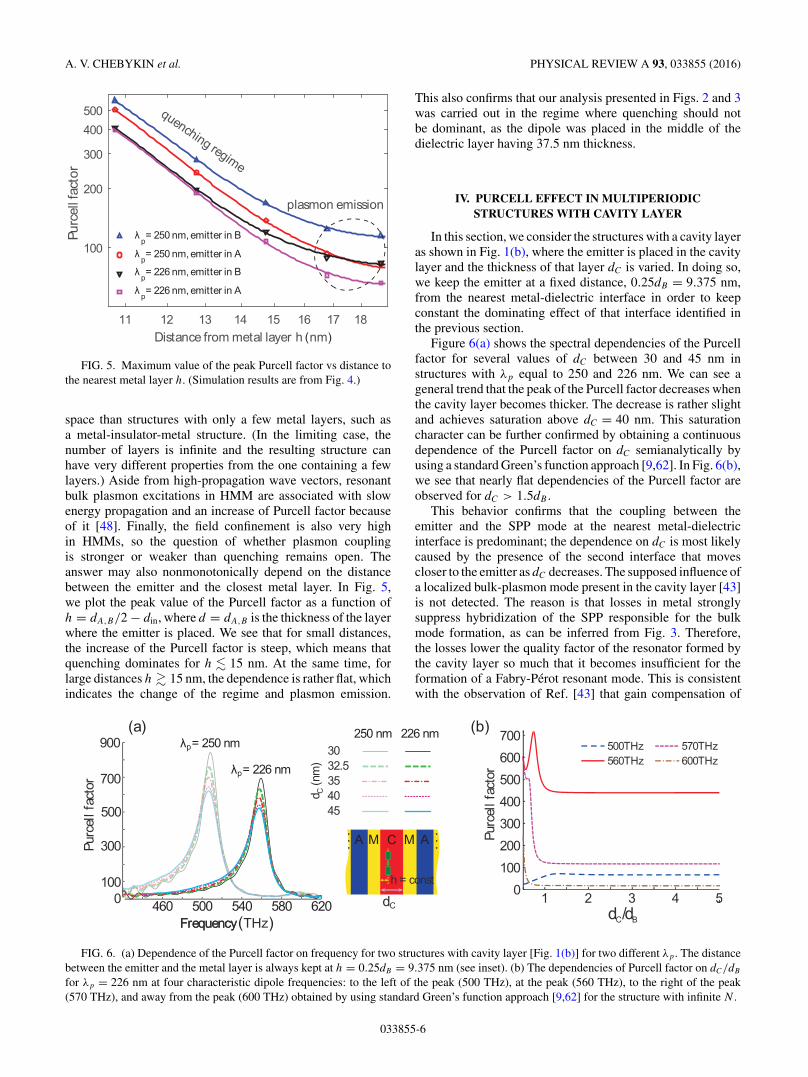
In this section, we consider the structures with a cavity layeras shown in Fig. 1(b), where the emitter is placed in the cavitylayer and the thickness of that layer dC is varied. In doing so,we keep the emitter at a fixed distance, 0.25dB = 9.375 nm,from the nearest metal-dielectric interface in order to keepconstant the dominating effect of that interface identified inthe previous section.
Figure 6(a) shows the spectral dependencies of the Purcellfactor for several values of dC between 30 and 45 nm instructures with λp equal to 250 and 226 nm. We can see ageneral trend that the peak of the Purcell factor decreases whenthe cavity layer becomes thicker. The decrease is rather slightand achieves saturation above dC = 40 nm. This saturationcharacter can be further confirmed by obtaining a continuousdependence of the Purcell factor on dC semianalytically byusing a standard Green’s function approach [9,62]. In Fig. 6(b),we see that nearly flat dependencies of the Purcell factor areobserved for dC > 1.5dB .
This behavior confirms that the coupling between theemitter and the SPP mode at the nearest metal-dielectricinterface is predominant; the dependence on dC is most likelycaused by the presence of the second interface that movescloser to the emitter as dC decreases. The supposed influence ofa localized bulk-plasmon mode present in the cavity layer [43]is not detected. The reason is that losses in metal stronglysuppress hybridization of the SPP responsible for the bulkmode formation, as can be inferred from Fig. 3. Therefore,the losses lower the quality factor of the resonator formed bythe cavity layer so much that it becomes insufficient for theformation of a Fabry-Perot resonant mode. This is consistentwith the observation of Ref. [43] that gain compensation of
( )
FIG. 6. (a) Dependence of the Purcell factor on frequency for two structures with cavity layer [Fig. 1(b)] for two different λp . The distancebetween the emitter and the metal layer is always kept at h = 0.25dB = 9.375 nm (see inset). (b) The dependencies of Purcell factor on dC/dB
for λp = 226 nm at four characteristic dipole frequencies: to the left of the peak (500 THz), at the peak (560 THz), to the right of the peak(570 THz), and away from the peak (600 THz) obtained by using standard Green’s function approach [9,62] for the structure with infinite N .
033855-6

ENHANCEMENT OF THE PURCELL FACTOR . . . PHYSICAL REVIEW A 93, 033855 (2016)
( )
FIG. 7. Maximum value of Purcell factor vs distance to the closestmetal layer h, defined as h = dB − din for regular structures and ash = dC − din for the structures with cavity (dC = 45 nm). Marksshow results of numerical simulations.
losses [63] was needed to observe the localized bulk mode intransmission-scenario experiments.
The dependence of the Purcell factor at a fixed frequency ondC/dB in the range below 1.5, as shown in Fig. 6(b), can havedifferent character depending on the choice of the frequencywith respect to the location of the peak in Fig. 6(a). It canchange from an increasing function for frequencies below thepeak to a generally decreasing dependence for frequenciesabove the peak to a sharp drop at frequencies further awayfrom the peak. At the peak frequency, the function has a morecomplicated nonmonotonic nature, having a maximum fordC � 0.75dB . These semianalytical calculations confirm thenumerical simulation results of CST MICROWAVE STUDIO.
Finally, we compare the Purcell effect in biperiodic struc-tures with and without a cavity layer for different cavitythickness dC and emitter placement within the cavity din.Similar to the previous case, we have calculated the maximumvalues of the Purcell factor and analyzed their dependence onthe distance to the nearest metal boundary, h (Fig. 7). As wecan see, the Purcell factor in the structures with dC > dB is lessthan in regular structures; this behavior persists for differentλp and is observed for all values of din (see Fig. 7). On theother hand, the Purcell factor can be greatly increased in thestructure with dC < dB (Fig. 8). For the case dC = 0.8dB ,which approximately corresponds to the maximum of thesolid-line dependence in Fig. 6(b), the Purcell factor is seen toincrease by a factor of 3–9, depending on din.
The comparison between regular and cavity-based biperi-odic structures reveals that even though the cavity structuresdo not bring fundamentally new effects for our choice ofparameters, the interplay between SPP excitations at differentmetal-dielectric boundaries can be significantly influenced byvarying the cavity layer thickness. As a result, the enhancementof the Purcell effect stemming from the multiperiodicity(namely, from εB �= εA, see Fig. 3) can be further controlledby the proper choice of the thickness of the layer containingthe emitting center in question.
FIG. 8. Comparison of Purcell-factor dependencies on frequencyfor regular [Fig. 1(a)] and for structures with a cavity central layer[Fig. 1(b)] with dC = 45 and 30 nm for (a) din = 0 (emitter at thecavity layer center) and (b) din = 12 nm (comparable to the case ofFig. 6).
V. CONCLUSIONS
We have theoretically studied the spontaneous emissionenhancement (the Purcell effect) in biperiodic hyperboliclikemetamaterials, i.e., periodic metal-dielectric multilayers wherethe odd-numbered dielectric layers have different dielectricpermittivity from the even-numbered dielectric layers, re-sulting in a geometry that can be coded as (MAMB)N ,where N is the number of periods. We have shown that thepresence of multiperiodicity affects the spontaneous emissionenhancement experienced by a point-dipole emitter placed inone of the dielectric layers, with the Purcell factors greaterthan in ordinary periodic hyperbolic metamaterial, and havecharacterized this additional enhancement with respect to theemitter placement and multilayer composition.
We have explicitly demonstrated that this Purcell-factorenhancement is primarily attributed to the surface excitationat the metal-dielectric interface closest to the emitter, whichis the expected behavior for an emitter brought close to ametallic surface. Nevertheless, the degree of enhancementwas found to be much stronger in multiperiodic structureswhere there are several distinct surface plasmon excitationscompared to the regular periodic multilayers with only onekind of such SPP modes. Most likely, this behavior is due tothe multiple-band character of the dispersion relation of themultiperiodic structures, so that a larger portion of the k spacebecomes populated by propagating states that the emitter cancouple with. Another, related increase of the Purcell factor wasobserved close to the region where the effective permittivityreaches near-zero values, again because the dispersion relationbecomes more extended in k space.
033855-7

A. V. CHEBYKIN et al. PHYSICAL REVIEW A 93, 033855 (2016)
We have also found out that structures with a “cav-ity” layer (i.e., with a layer whose thickness has beenaltered compared to the other layers of the same type)can bring about an additional Purcell-factor enhancementresulting from the interplay between surface plasmon exci-tations at the two metal-dielectric interfaces closest to theemitter.
We would like to point out that according to [47,51,52],one can further increase the Purcell factor by decreasing thedielectric and metal layer thicknesses and choosing metals withlower losses. Nevertheless, the goal of this paper is to studythe effect of multiperiodicity of HMM rather than to engineera structure with maximum Purcell factor, so we have focusedon the general properties of the structure under considerationand did not perform optimization.
The combined action of all the described enhancementmechanisms can cause the Purcell factor to be more than anorder of magnitude stronger compared to what one wouldexpect by naively treating the multilayer in the effectivemedium approximation, i.e., without regard for its internalstructure. Besides improving our understanding of light-matterinteraction in complex plasmonic metamaterials, our resultsshow that plasmonic multilayers with an internal structure
that is only slightly more complex than a simple alternationof metal and dielectric layers can be used to tailor suchproperties as spontaneous emission of embedded atoms withhigh versatility.
ACKNOWLEDGMENTS
We are grateful to Alexander Poddubny and Yuri Kivsharfor suggestions during manuscript preparation. One of us(S.V.Z.) wishes to acknowledge partial financial supportfrom the People Programme (Marie Curie Actions) of theEuropean Unions 7th Framework Programme FP7-PEOPLE-2011-IIF under REA Grant Agreement No. 302009 (ProjectHyPHONE). This work was financially supported by the Gov-ernment of the Russian Federation, Grant No. 074-U01, by theMinistry of Education and Science of the Russian Federation(Zadanie No. 3.1231.2014/K and Project No. 11.G34.31.0020,GOSZADANIE 2014/190, Zadanie No. 3.561.2014/K and No.14.584.21.0009 10), by the Russian Foundation for BasicResearch (Grants No. 14-02-31270 and No. 14-07-31272),and the Dynasty Foundation (Russia).
[1] H. N. S. Krishnamoorthy, Z. Jacob, E. Narimanov, I. Kret-zschmar, and V. M. Menon, Science 336, 205 (2012).
[2] J. Luo, H. Chen, B. Hou, P. Xu, and Y. Lai, Plasmonics 8, 1095(2013).
[3] J. Valentine, S. Zhang, T. Zentgraf, E. Ulin-Avila, D. A. Genov,G. Bartal, and Xiang Zhang, Nature 455, 376 (2008).
[4] E. Verhagen, R. de Waele, L. Kuipers, and A. Polman, Phys.Rev. Lett. 105, 223901 (2010).
[5] T. Xu, A. Agrawal, M. Abashin, K. J. Chau, and H. J. Lezec,Nature (London) 497, 470 (2013).
[6] M. Kuwata-Gonokami, N. Saito, Y. Ino, M. Kauranen, K. Jefi-movs, T. Vallius, J. Turunen, and Y. Svirko, Phys. Rev. Lett. 95,227401 (2005).
[7] G. Castaldi, V. Galdi, A. Alu, and N. Engheta, Phys. Rev. Lett.108, 063902 (2012).
[8] Z. Jacob, I. I. Smolyaninov, and E. E. Narimanov, Appl. Phys.Lett. 100, 181105 (2012).
[9] I. Iorsh, A. Poddubny, A. Orlov, P. Belov, and Y. S. Kivshar,Phys. Lett. A 376, 185 (2012).
[10] A. V. Chebykin, A. A. Orlov, C. R. Simovski, Y. S. Kivshar, andP. A. Belov, Phys. Rev. B 86, 115420 (2012).
[11] A. Poddubny, I. Iorsh, P. Belov, and Y. Kivshar, Nat. Photonics7, 948 (2013).
[12] D. R. Smith, D. Schurig, J. J. Mock, P. Kolinko, and P. Rye,Appl. Phys. Lett. 84, 13 (2004).
[13] D. Smith, P. Kolinko, and D. Schurig, J. Opt. Soc. Am. B 21,1032 (2004).
[14] A. Degiron, D. Smith, J. Mock, B. Justice, and J.Gollub, Appl. Phys. A: Mater. Sci. Process. 87, 321(2007).
[15] W. Yan, L. Shen, L. Ran, and J. A. Kong, J. Opt. Soc. Am. A24, 530 (2007).
[16] V. P. Drachev, V. A. Podolskiy, and A. V. Kildishev, Opt. Express21, 15048 (2013).
[17] Z. Jacob, L. V. Alekseyev, and E. Narimanov, Opt. Express 14,8247 (2006).
[18] Z. Jacob, J.-Y. Kim, G. V. Naik, A. Boltasseva, E. E. Narimanov,and V. M. Shalaev, Appl. Phys. B: Lasers Opt. 100, 215(2010).
[19] M. Y. Shalaginov, V. V. Vorobyov, J. Liu, M. Ferrera, A. V.Akimov, A. Lagutchev, A. N. Smolyaninov, V. V. Klimov,J. Irudayaraj, A. V. Kildishev et al., Laser Photonics Rev. 9,120 (2015).
[20] J. K. Kitur, L. Gu, T. Tumkur, C. Bonner, and M. A. Noginov,ACS Photonics 2, 1019 (2015).
[21] K. L. Tsakmakidis, A. D. Boardman, and O. Hess, Nature(London) 450, 397 (2007).
[22] H. Hu, D. Ji, X. Zeng, K. Liu, and Q. Gan, Sci. Rep. 3, 1249(2013).
[23] M. A. K. Othman, C. Guclu, and F. Capolino, Opt. Express 21,7614 (2013).
[24] A. D. Neira, N. Olivier, M. E. Nasir, W. Dickson, G. A. Wurtz,and A. V. Zayats, Nat. Commun. 6, 7757 (2015).
[25] G. A. Wurtz, R. Pollard, W. Hendren, G. Wiederrecht, D. Gosz-tola, V. Podolskiy, and A. V. Zayats, Nat. Nanotechnol. 6, 107(2011).
[26] C. Simovski, S. Maslovski, I. Nefedov, and S. Tretyakov, Opt.Express 21, 14988 (2013).
[27] S. Lang, M. Tschikin, S.-A. Biehs, A. Y. Petrov, and M. Eich,Appl. Phys. Lett. 104, 121903 (2014).
[28] X. Liu, T. Bright, and Z. Zhang, J. Heat Transfer 136, 092703(2014).
[29] J. Yao, Z. Liu, Y. Liu, Y. Wang, C. Sun, G. Bartal, A. M. Stacy,and X. Zhang, Science 321, 930 (2008).
033855-8

ENHANCEMENT OF THE PURCELL FACTOR . . . PHYSICAL REVIEW A 93, 033855 (2016)
[30] W. Dickson, G. A. Wurtz, P. Evans, D. O’Connor, R. Atkinson,R. Pollard, and A. V. Zayats, Phys. Rev. B 76, 115411 (2007).
[31] A. Kabashin, P. Evans, S. Pastkovsky, W. Hendren, G. Wurtz,R. Atkinson, R. Pollard, V. Podolskiy, and A. Zayats, Nat. Mater.8, 867 (2009).
[32] N. Vasilantonakis, M. E. Nasir, W. Dickson, G. A. Wurtz, andA. V. Zayats, Laser Photonics Rev. 9, 345 (2015).
[33] M. A. Noginov, Y. A. Barnakov, G. Zhu, T. Tumkur, H. Li, andE. E. Narimanov, Appl. Phys. Lett. 94, 151105 (2009).
[34] M. A. Noginov, H. Li, Y. A. Barnakov, D. Dryden, G. Nataraj,G. Zhu, C. E. Bonner, M. Mayy, Z. Jacob, and E. E. Narimanov,Opt. Lett. 35, 1863 (2010).
[35] J. Kanungo and J. Schilling, Appl. Phys. Lett. 97, 021903 (2010).[36] I. Avrutsky, I. Salakhutdinov, J. Elser, and V. Podolskiy, Phys.
Rev. B 75, 241402 (2007).[37] S. Ishii, A. V. Kildishev, E. Narimanov, V. M. Shalaev, and V. P.
Drachev, Laser Photonics Rev. 7, 265 (2013).[38] O. Kidwai, S. V. Zhukovsky, and J. E. Sipe, Phys. Rev. A 85,
053842 (2012).[39] S. V. Zhukovsky, O. Kidwai, and J. E. Sipe, Opt. Express 21,
14982 (2013).[40] A. V. Chebykin, A. A. Orlov, A. V. Vozianova, S. I. Maslovski,
Y. S. Kivshar, and P. A. Belov, Phys. Rev. B 84, 115438 (2011).[41] V. A. Podolskiy, P. Ginzburg, B. Wells, and A. V. Zayats, Faraday
Discuss. 178, 61 (2015).[42] A. A. Orlov, A. K. Krylova, S. V. Zhukovsky, V. E. Babicheva,
and P. A. Belov, Phys. Rev. A 90, 013812 (2014).[43] S. V. Zhukovsky, A. A. Orlov, V. E. Babicheva, A. V.
Lavrinenko, and J. E. Sipe, Phys. Rev. A 90, 013801 (2014).[44] V. N. Smolyaninova, B. Yost, D. Lahneman, E. E. Narimanov,
and I. I. Smolyaninov, Sci. Rep. 4, 5706 (2014).[45] E. E. Narimanov, Phys. Rev. X 4, 041014 (2014).[46] S. V. Zhukovsky, S. V. Gaponenko, and A. V. Lavrinenko,
in Optics of Aperiodic Structures–Fundamentals and DeviceApplications, edited by L. Dal Negro (Pan Stanford Publishing,Singapore, 2014).
[47] Y. C. Jun, R. D. Kekatpure, J. S. White, and M. L. Brongersma,Phys. Rev. B 78, 153111 (2008).
[48] P. Yao, C. Van Vlack, A. Reza, M. Patterson, M. M. Dignam,and S. Hughes, Phys. Rev. B 80, 195106 (2009).
[49] G. Ford and W. Weber, Phys. Rep. 113, 195 (1984).[50] A. Kinkhabwala, Z. Yu, S. Fan, Y. Avlasevich, K. Mullen, and
W. Moerner, Nat. Photonics 3, 654 (2009).[51] R. R. Chance, A. Prock, and R. Silbey, in Advances in Chemical
Physics, Vol. 37, edited by I. Prigogine and Stuart A. Rice (JohnWiley & Sons, Inc., Hoboken, NJ, 1978).
[52] G. M. Akselrod, C. Argyropoulos, T. B. Hoang, C. Ciracı,C. Fang, J. Huang, D. R. Smith, and M. H. Mikkelsen, Nat.Photonics 8, 835 (2014).
[53] A. A. Orlov, I. V. Iorsh, S. V. Zhukovsky, and P. A. Belov,Photonics Nanostruct. 12, 213 (2014).
[54] A. V. Chebykin, A. A. Orlov, A. S. Shalin, A. N. Poddubny, andP. A. Belov, Phys. Rev. B 91, 205126 (2015).
[55] A. E. Krasnok, D. S. Filonov, C. R. Simovski, Y. S. Kivshar,and P. A. Belov, Appl. Phys. Lett. 104, 133502 (2014).
[56] A. E. Krasnok, A. P. Slobozhanyuk, C. R. Simovski, S. A.Tretyakov, A. N. Poddubny, A. E. Miroshnichenko, Y. S.Kivshar, and P. A. Belov, Sci. Rep. 5, 12956 (2015).
[57] R. Chance, A. Prock, and R. Silbey, Adv. Chem. Phys. 37, 1(1978).
[58] D. N. Chigrin, D. Kumar, D. Cuma, and G. von Plessen, ACSPhotonics 3, 27 (2016).
[59] R. Faggiani, J. Yang, and P. Lalanne, ACS Photonics 2, 1739(2015).
[60] C. Belacel, B. Habert, F. Bigourdan, F. Marquier, J.-P. Hugonin,S. M. de Vasconcellos, X. Lafosse, L. Coolen, C. Schwob,C. Javaux et al., Nano Lett. 13, 1516 (2013).
[61] J. Yang, R. Faggiani, and P. Lalanne, Nanoscale Horiz. 1, 11(2016).
[62] M. S. Tomas and Z. Lenac, Phys. Rev. A 60, 2431 (1999).[63] X. Ni, S. Ishii, M. D. Thoreson, V. M. Shalaev, S. Han, S. Lee,
and A. V. Kildishev, Opt. Express 19, 25242 (2011).
033855-9