Embed Size (px)
Citation preview

Materials Research Bulletin 47 (2012) 2708–2712
Enhanced H2S gas sensing properties of multiple-networked Pd-dopedSnO2-core/ZnO-shell nanorod sensors
Hyunsu Kim, Changhyun Jin, Sunghoon Park, Chongmu Lee *
Department of Materials Science and Engineering, Inha University, Incheon 402-751, Republic of Korea
A R T I C L E I N F O
Article history:
Available online 24 April 2012
Keywords:
A. Oxides
A. Semiconductors
A. Vapor deposition
B. Electrical properties
C. Electron diffraction
A B S T R A C T
Pd-doped SnO2-core/ZnO-shell nanorods were synthesized by using a three-step process: thermal
evaporation of Sn powders in an oxygen atmosphere, atomic layer deposition of ZnO, and Pd diffusion
followed by annealing. The sensitivity of the multiple networked SnO2-core/ZnO-shell nanorod sensor to
H2S gas was found to be improved further significantly by Pd doping. The Pd-doped SnO2-core/ZnO-shell
nanorod sensor showed sensitivities of 6.4, 15.4, and 36.2% at H2S concentrations of 20, 50, and 100 ppm
at room temperature. The sensitivity of the nanorods was improved by more than 10 times at a H2S
concentration of 100 ppm. The sensitivity enhancement of the SnO2-core/ZnO-shell nanorods by Pd
doping may be attributed to the spillover effect, active reaction site generation, and the enhancement of
chemisorption and dissociation of gas.
Crown Copyright � 2012 Published by Elsevier Ltd. All rights reserved.
Contents lists available at SciVerse ScienceDirect
Materials Research Bulletin
jo u rn al h om ep age: ww w.els evier .c o m/lo c ate /mat res b u
1. Introduction
In recent years, one-dimensional (1D) nanostructures havebecome a focus of intensive research owing to their uniqueproperties and applications [1–9]. As sensors 1D nanostructureshave the advantages of higher sensitivity, superior spatialresolution, and rapid response associated with individual nanos-tructures due to the high surface-to-volume ratios compared tothin film gas sensors [10–12]. SnO2 and ZnO are the mostcommonly used materials for gas sensors. However, these sensingmaterials have shortcomings such as poor selectivity andreliability because they react with several gases simultaneously.Various techniques including surface functionalization [13–15],doping [16–18], and heterostructure formation [19–21] have beendeveloped to solve this problem. Based on one of these techniques,SnO2-core/ZnO-shell nanorod sensors have been proposed as acountermeasure against this problem [22–26]. Several researchgroups demonstrated that the SnO2-core/ZnO-shell 1D nanos-tructures could enhance the O2, NO2, H2, H2S, and C2H5OH gassensing properties of the normal 1D nanostructures. However, it isstill necessary to examine if the gas sensing property of the SnO2-core/ZnO-shell 1D nanostructure sensors can be further enhancedby surface functionalization or doping technique. In this work, wefabricated SnO2-core/ZnO-shell 1D nanostructures doped with Pdusing a three-step process: thermal evaporation of Sn powders,
* Corresponding author. Tel.: +82 32 860 7536; fax: +82 32 862 5546.
E-mail address: [email protected] (C. Lee).
0025-5408/$ – see front matter . Crown Copyright � 2012 Published by Elsevier Ltd. A
http://dx.doi.org/10.1016/j.materresbull.2012.04.038
atomic layer deposition of ZnO and Pd diffusion followed byannealing and examined their H2S gas sensing properties.
2. Experimental
Gold (Au) thin films used as a catalyst were deposited on p-typeSi (1 0 0) substrates by direct current (DC) sputtering for 3 nmthickness. SnO2 1D nanostructures were synthesized on the Au-coated p-type Si (1 0 0) substrate by the thermal evaporation of Snpowders at 900 8C for 1 h in an oxygen atmosphere. The Snpowders were loaded onto a small alumina boat and positioned atthe center of the horizontal quartz tube at the total gas pressure of1 Torr. The gas flow rates of N2 and O2 were 300 and 10 sccm,respectively. Next, the Si substrate with the as-synthesized SnO2
nanorods was transferred to an ALD chamber to deposit a ZnO thinfilm on the nanorods. ZnO coating was conducted on thenanostructures. Diethylzinc (DEZn) and H2O were kept in bubblersat 10 8C. These source gases were alternatively fed into thechamber through separate inlet lines and nozzles. The typical pulselengths were 0.15 s for DEZn, 0.2 s for H2O and 3 s for purging thereactants. The substrate temperature and pressure in the chamberwere set to 150 8C and 0.1 Torr, respectively. The ALD process timefor ZnO coating was 1 h. In the doping of Pd, 40 ml ethanol solutionof palladium chloride (ethanol: PdCl2 = 1000:1) was poured ontothe SnO2-core/ZnO-shell 1D nanostructures. Subsequently, theSnO2-core/ZnO-shell 1D nanostructures were transferred to anannealing furnace and annealed at 350 8C in an Ar atmosphere for30 min to make the Pd diffuse into the nanostructures. The Ar gasflow rate and process pressure were 100 standard cubic centimeterper minute (sccm) and 0.1 Torr, respectively. The Pd concentration
ll rights reserved.

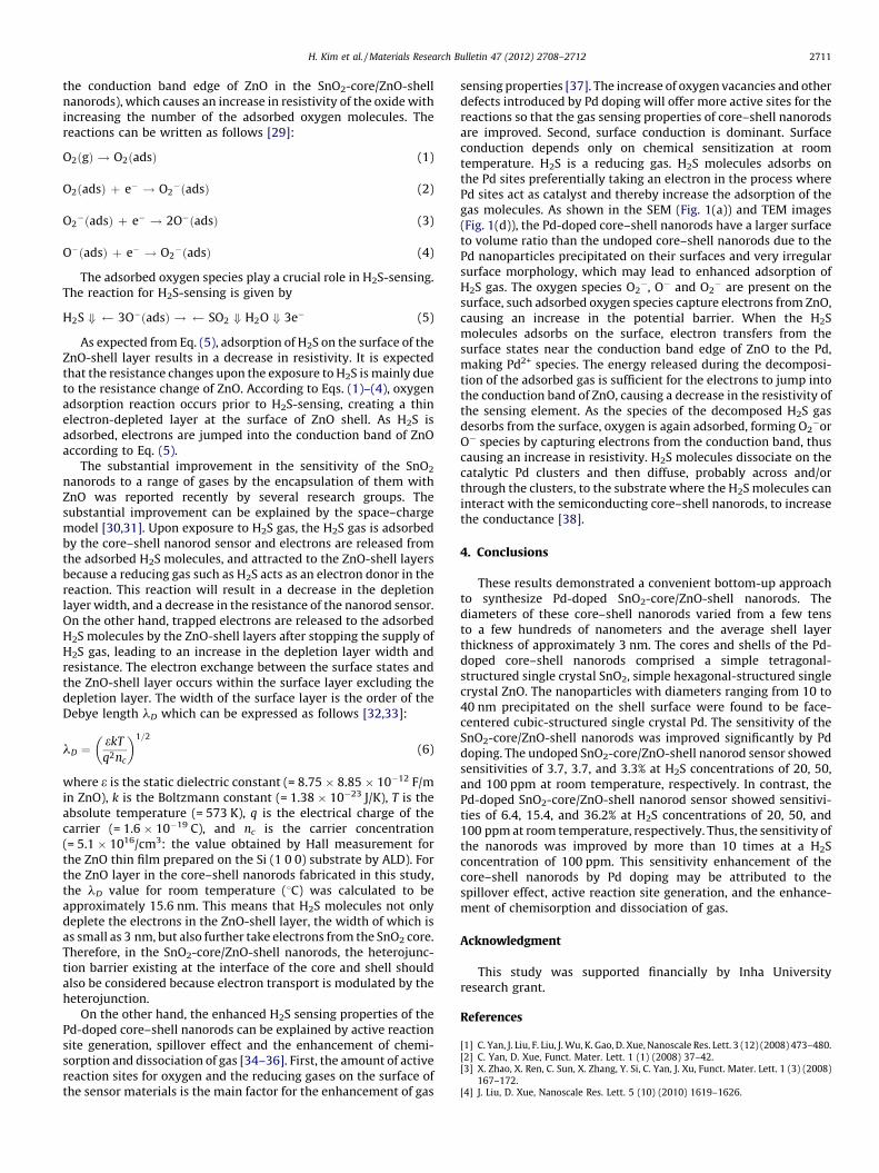
Fig. 1. (a) SEM images of the Pd-doped SnO2-core/ZnO-shell nanorods synthesized on the Si(100) substrate. Inset, Enlarged SEM image of a typical Pd-doped SnO2-core/ZnO-
shell nanorods. (b) EDX spectra of a typical Pd-doped core–shell nanorod. (c) XRD patterns of Pd-doped SnO2-core/ZnO-shell nanorods. (d) Low-magnification TEM image of a
typical Pd-doped SnO2-core/ZnO-shell nanorod. (e) HRTEM image and (f) SAED pattern of a typical Pd-doped SnO2-core/ZnO-shell nanorod.
H. Kim et al. / Materials Research Bulletin 47 (2012) 2708–2712 2709
in the Pd-doped SnO2-core/ZnO-shell 1D nanostructures wasestimated by calculating the weight ratio of Pd in the ethanolsolution of PdCl2 to the core–shell 1D nanostructures.
The collected products were characterized by using a fieldemission scanning electron microscope (FESEM, Hitachi S-4200)and a high-resolution transmission electron microscope (HRTEM)(JEM 2100F JEOL) equipped with an energy dispersive X-rayspectrometer (EDXS). X-ray diffraction (XRD) analyses were alsoperformed an X-ray diffractometer (Philips X’pert MRD) with Cu-Ka radiation. In the XRD measurements, a glancing angle (0.58) wasused to minimize the contribution from the substrate.
For sensing measurement, Ni (�200 nm in thickness) and Au(�50 nm) thin films were sequentially deposited by sputtering toform electrodes using an interdigital electrode (IDE) mask. SnO2-core/ZnO-shell nanorod gas sensors were fabricated by pouring afew drops of nanorod-suspended ethanol onto oxidized Sisubstrates equipped with a pair of IDEs with a gap length of
20 mm. The structure of the multiple networked core–shellnanorod sensors is shown in Fig. 1. The electrical and gas sensingproperty measurements of the undoped- and Pd-doped SnO2-core/ZnO-shell nanorods were carried out at room temperature in aquartz tube inserted in an electrical furnace. During the measure-ments, the nanorod gas sensors were placed in a sealed quartz tubewith an electrical feed through. A given amount of H2S (>99.99%)gas was injected into the testing tube by a microsyringe to obtainthe H2S concentrations 20, 50, and 100 ppm while the electricalresistance of the nanorods was monitored. The sensitivity wasdefined as Ra/Rg for H2S gas where Ra and Rg are the electricalresistances of sensors in air and the target gas, respectively. Theresponse time was defined as the time required for the variation inelectrical resistance to reach 90% of the equilibrium value after H2Swas injected and the recovery time as the time needed for thesensor to return to 90% above the original resistance in air after H2Sbeing removed.

Fig. 2. Electrical responses of gas sensors to H2S gas at room temperature fabricated
from undoped- and Pd-doped SnO2-core/ZnO-shell nanorod sensors: (a) response
curve of undoped SnO2-core/ZnO-shell nanorod sensor, (b) response curve of Pd
doped SnO2-core/ZnO-shell nanorod sensor.
H. Kim et al. / Materials Research Bulletin 47 (2012) 2708–27122710
3. Results and discussion
Fig. 1(a) shows a SEM image of the Pd-doped SnO2-core/ZnO-shell 1D nanostructures synthesized using the three steps. Theproducts are rod-like nanorods decorated with nanoparticles. Thediameters of the nanorods ranged from a few tens to a fewhundreds of nanometers and their lengths were up to several tensof micrometers. The diameters of the nanoparticles ranged from 10to 40 nm (inset in Fig. 1(a)). The EDX spectra (Fig. 1(b)) confirmthat the core–shell nanorods contained elemental Sn, Zn, O, and Pd.
XRD analyses were performed to examine the structures of theas-synthesized SnO2-core/ZnO-shell nanorods. In the XRD patternsof the as-synthesized SnO2 nanorods (Fig. 1(c)), nine reflectionscharacteristic of simple tetragonal-structured single crystal SnO2
with lattice parameters a = 0.4738 nm and c = 0.3187 nm (JCPDSCard: 41-1445) are identified. Besides the reflections from SnO2
cores (0 0 2) and (2 0 0) reflections from simple hexagonal-structured ZnO with lattice parameters a = 0.3249 nm, andc = 0.5206 nm (JCPDS No: 36-1451) are identified, implying thatZnO shells are also crystalline. Lack of a Pd reflection peak in theXRD pattern as well as the small Pd peak in the EDX spectraindicates that the small amount of Pd doped into the nanorodcompared to those of SnO2 and ZnO.
For further structural study of the sample, TEM observationswere carried out. The low-magnification TEM image of a typicalcore–shell nanorod is presented in Fig. 1(d). The average thicknessof the ZnO-shell layers appears to be approximately 3 nm. Fig. 1(e)and (f) display the local high-resolution TEM (HRTEM) image andcorresponding selected area electron diffraction (SAED) pattern ofthe core–shell interface region, respectively. The HRTEM imagetaken at the core–shell interface region shows a SnO2 core (a darkregion) with a thin ZnO-shell layer (a less dark region) with auniform thickness. The HRTEM image with the SAED pattern forthe core–shell nanorods is in good agreement with the XRDanalysis results. The resolved spacings of two neighboring parallelfringes in the core and shell regions were approximately 0.23 nm(SnO2-core), 0.26 nm (ZnO-shell), and 0.19 nm (Pd particle),corresponding to the (2 0 0) lattice plane of simple tetragonalSnO2, the (0 0 2) lattice plane of simple hexagonal ZnO, and the(0 0 2) lattice plane of face-centered cubic Pd, respectively. Thecorresponding SAED pattern (Fig. 1(f)) shows only the reflectionspots of simple tetragonal-structured single crystal SnO2. Those ofZnO and Pd may be too dim to be observed.
The dynamic sensing properties of the SnO2-core/ZnO-shellnanorods were examined at room temperature. The curves inFig. 2(a) and (b) shows the dynamic responses of multiplenetworked undoped- and Pd-doped SnO2-core/ZnO-shell nanorodsensors, respectively, to a reducing gas H2S. The resistanceresponded well to the H2S gas. The resistance decreased quicklywhen the nanorod sensors were exposed to H2S gas and theresistance recovered completely to the initial value when H2S gassupply was stopped and air was introduced. The sensor responsesto H2S gas were also stable and reproducible for repeated testingcycles. The sensing properties of the undoped- and Pd-doped core–shell nanorod sensors are summarized in Table 1. The response andrecovery times of the Pd-doped SnO2-core/ZnO-shell nanorod
Table 1H2S gas sensitivities, response times, and recovery times of undoped and Pd-doped Sn
H2S Conc. Sensitivity (%) Response
SnO2–ZnO Pd–SnO2–ZnO SnO2–ZnO
100 ppm 3.3 36.2 900
50 ppm 3.7 15.4 900
20 ppm 3.7 6.4 900
sensor are somewhat longer than those of the undoped SnO2-core/ZnO-shell nanorod sensor. On the other hand, the sensitivity to H2Sgas was improved significantly by Pd doping. The undoped SnO2-core/ZnO-shell nanorod sensor showed sensitivities of 3.7, 3.7, and3.3% at H2S concentrations of 20, 50, and 100 ppm at roomtemperature, respectively. In contrast, Pd-doped SnO2-core/ZnO-shell nanorod sensor showed sensitivities of 6.4, 15.4, and 36.2% atH2S concentrations of 20, 50, and 100 ppm at room temperature,respectively. Thus, the sensitivity of the nanorods was improved bymore than 10 times at a H2S concentration of 100 ppm.
It is well known that the sensing mechanism of the oxidematerials is surface controlled in which the grain size, surfacestates and oxygen adsorption play an important role [27,28].Therefore, oxide 1D nanostructures have larger surface and thushave higher sensitivity. Before introducing the H2S, the sensorabsorbs O2 from air. The change of electrical resistance isdependent on the species and the amount of chemisorbed oxygenon the surface. The adsorbed oxygen molecules transform intooxygen ions (O�, O2� and O2
�) by capturing free electrons from theconduction band of the sensing metal oxide (the surface states near
O2-core/ZnO-shell nanorod sensors.
time (s) Recovery time (s)
Pd–SnO2–ZnO SnO2–ZnO Pd–SnO2–ZnO
1250 800 650
1100 800 750
1100 800 1100
H. Kim et al. / Materials Research Bulletin 47 (2012) 2708–2712 2711
the conduction band edge of ZnO in the SnO2-core/ZnO-shellnanorods), which causes an increase in resistivity of the oxide withincreasing the number of the adsorbed oxygen molecules. Thereactions can be written as follows [29]:
O2ðgÞ ! O2ðadsÞ (1)
O2ðadsÞ þ e� ! O2�ðadsÞ (2)
O2�ðadsÞ þ e� ! 2O�ðadsÞ (3)
O�ðadsÞ þ e� ! O2�ðadsÞ (4)
The adsorbed oxygen species play a crucial role in H2S-sensing.The reaction for H2S-sensing is given by
H2S + 3O�ðadsÞ ! SO2 + H2O + 3e� (5)
As expected from Eq. (5), adsorption of H2S on the surface of theZnO-shell layer results in a decrease in resistivity. It is expectedthat the resistance changes upon the exposure to H2S is mainly dueto the resistance change of ZnO. According to Eqs. (1)–(4), oxygenadsorption reaction occurs prior to H2S-sensing, creating a thinelectron-depleted layer at the surface of ZnO shell. As H2S isadsorbed, electrons are jumped into the conduction band of ZnOaccording to Eq. (5).
The substantial improvement in the sensitivity of the SnO2
nanorods to a range of gases by the encapsulation of them withZnO was reported recently by several research groups. Thesubstantial improvement can be explained by the space–chargemodel [30,31]. Upon exposure to H2S gas, the H2S gas is adsorbedby the core–shell nanorod sensor and electrons are released fromthe adsorbed H2S molecules, and attracted to the ZnO-shell layersbecause a reducing gas such as H2S acts as an electron donor in thereaction. This reaction will result in a decrease in the depletionlayer width, and a decrease in the resistance of the nanorod sensor.On the other hand, trapped electrons are released to the adsorbedH2S molecules by the ZnO-shell layers after stopping the supply ofH2S gas, leading to an increase in the depletion layer width andresistance. The electron exchange between the surface states andthe ZnO-shell layer occurs within the surface layer excluding thedepletion layer. The width of the surface layer is the order of theDebye length lD which can be expressed as follows [32,33]:
lD ¼ekT
q2nc
� �1=2
(6)
where e is the static dielectric constant (= 8.75 � 8.85 � 10�12 F/min ZnO), k is the Boltzmann constant (= 1.38 � 10�23 J/K), T is theabsolute temperature (= 573 K), q is the electrical charge of thecarrier (= 1.6 � 10�19 C), and nc is the carrier concentration(= 5.1 � 1016/cm3: the value obtained by Hall measurement forthe ZnO thin film prepared on the Si (1 0 0) substrate by ALD). Forthe ZnO layer in the core–shell nanorods fabricated in this study,the lD value for room temperature (8C) was calculated to beapproximately 15.6 nm. This means that H2S molecules not onlydeplete the electrons in the ZnO-shell layer, the width of which isas small as 3 nm, but also further take electrons from the SnO2 core.Therefore, in the SnO2-core/ZnO-shell nanorods, the heterojunc-tion barrier existing at the interface of the core and shell shouldalso be considered because electron transport is modulated by theheterojunction.
On the other hand, the enhanced H2S sensing properties of thePd-doped core–shell nanorods can be explained by active reactionsite generation, spillover effect and the enhancement of chemi-sorption and dissociation of gas [34–36]. First, the amount of activereaction sites for oxygen and the reducing gases on the surface ofthe sensor materials is the main factor for the enhancement of gas
sensing properties [37]. The increase of oxygen vacancies and otherdefects introduced by Pd doping will offer more active sites for thereactions so that the gas sensing properties of core–shell nanorodsare improved. Second, surface conduction is dominant. Surfaceconduction depends only on chemical sensitization at roomtemperature. H2S is a reducing gas. H2S molecules adsorbs onthe Pd sites preferentially taking an electron in the process wherePd sites act as catalyst and thereby increase the adsorption of thegas molecules. As shown in the SEM (Fig. 1(a)) and TEM images(Fig. 1(d)), the Pd-doped core–shell nanorods have a larger surfaceto volume ratio than the undoped core–shell nanorods due to thePd nanoparticles precipitated on their surfaces and very irregularsurface morphology, which may lead to enhanced adsorption ofH2S gas. The oxygen species O2
�, O� and O2� are present on the
surface, such adsorbed oxygen species capture electrons from ZnO,causing an increase in the potential barrier. When the H2Smolecules adsorbs on the surface, electron transfers from thesurface states near the conduction band edge of ZnO to the Pd,making Pd2+ species. The energy released during the decomposi-tion of the adsorbed gas is sufficient for the electrons to jump intothe conduction band of ZnO, causing a decrease in the resistivity ofthe sensing element. As the species of the decomposed H2S gasdesorbs from the surface, oxygen is again adsorbed, forming O2
�orO� species by capturing electrons from the conduction band, thuscausing an increase in resistivity. H2S molecules dissociate on thecatalytic Pd clusters and then diffuse, probably across and/orthrough the clusters, to the substrate where the H2S molecules caninteract with the semiconducting core–shell nanorods, to increasethe conductance [38].
4. Conclusions
These results demonstrated a convenient bottom-up approachto synthesize Pd-doped SnO2-core/ZnO-shell nanorods. Thediameters of these core–shell nanorods varied from a few tensto a few hundreds of nanometers and the average shell layerthickness of approximately 3 nm. The cores and shells of the Pd-doped core–shell nanorods comprised a simple tetragonal-structured single crystal SnO2, simple hexagonal-structured singlecrystal ZnO. The nanoparticles with diameters ranging from 10 to40 nm precipitated on the shell surface were found to be face-centered cubic-structured single crystal Pd. The sensitivity of theSnO2-core/ZnO-shell nanorods was improved significantly by Pddoping. The undoped SnO2-core/ZnO-shell nanorod sensor showedsensitivities of 3.7, 3.7, and 3.3% at H2S concentrations of 20, 50,and 100 ppm at room temperature, respectively. In contrast, thePd-doped SnO2-core/ZnO-shell nanorod sensor showed sensitivi-ties of 6.4, 15.4, and 36.2% at H2S concentrations of 20, 50, and100 ppm at room temperature, respectively. Thus, the sensitivity ofthe nanorods was improved by more than 10 times at a H2Sconcentration of 100 ppm. This sensitivity enhancement of thecore–shell nanorods by Pd doping may be attributed to thespillover effect, active reaction site generation, and the enhance-ment of chemisorption and dissociation of gas.
Acknowledgment
This study was supported financially by Inha Universityresearch grant.
References
[1] C. Yan, J. Liu, F. Liu, J. Wu, K. Gao, D. Xue, Nanoscale Res. Lett. 3 (12) (2008) 473–480.[2] C. Yan, D. Xue, Funct. Mater. Lett. 1 (1) (2008) 37–42.[3] X. Zhao, X. Ren, C. Sun, X. Zhang, Y. Si, C. Yan, J. Xu, Funct. Mater. Lett. 1 (3) (2008)
167–172.[4] J. Liu, D. Xue, Nanoscale Res. Lett. 5 (10) (2010) 1619–1626.

H. Kim et al. / Materials Research Bulletin 47 (2012) 2708–27122712
[5] J. Liu, D. Xue, Nanoscale Res. Lett. 5 (10) (2010) 1525–1534.[6] J. Wu, D. Xue, Nanoscale Res. Lett. 6 (2011) 14.[7] J. Liu, D. Xue, K. Li, Nanoscale Res. Lett. 6 (2011) 138.[8] C. Jin, H. Kim, W.I. Lee, C. Lee, Adv. Mater. 23 (2011) 1982–1987.[9] C. Jin, H. Kim, H.Y. Ryu, H.W. Kim, C. Lee, J. Phys. Chem. C 115 (2011) 8513–8518.
[10] A. Kolmakov, Y. Zhang, G. Cheng, M. Moskovits, Adv. Mater. 15 (2003) 997–1000.[11] Y. Liu, E. Koep, M. Liu, Chem. Mater. 17 (2005) 3997–4000.[12] M. Law, H. Kind, B. Messer, F. Kim, P.D. Yang, Angew. Chem. 114 (2002) 2511–2514.[13] Y.H. Lin, M.W. Huang, C.K. Liu, J.R. Chen, J.M. Wu, H.C. Shih, J. Electrochem. Soc.
156 (2009) K196–K199.[14] N.S. Ramgir, I.S. Mulla, K.P. Vijayamohanan, Sens. Actuators B 107 (2005) 708–
715.[15] Q. Wan, T.H. Wang, Chem. Commun. (Cambridge) 30 (2005) 3841–3843.[16] A. Kolmakov, D.O. Klenov, Y. Lilach, S. Stemmer, M. Moskovits, Nano Lett. 5 (2005)
667–673.[17] Q. Kuang, C.S. Lao, Z. Li, Y.Z. Liu, Z.X. Xie, L.S. Zheng, Z.L. Wang, J. Phys. Chem. C 112
(2008) 11539–11544.[18] J.S. Wright, W. Lim, B.P. Gila, S.J. Pearton, J.L.A. Johnson, Ural, f. Ren, Sens.
Actuators B 140 (2009) 196–199.[19] X. Xue, L. Xing, Y. Chen, S. Shi, Y. Wang, T. Wang, J. Phys. Chem. C 112 (2008)
12157–12160.[20] Y.J. Chen, C.L. Zhu, L.J. Wang, P. Gao, M.S. Cao, X.L. Shi, Nanotechnology 20 (2009)
045502–045507.
[21] J.Y. Park, S.W. Choi, J.W. Lee, C. Lee, S.S. Kim, J. Am. Ceram. Soc. 92 (2009) 2551–2554.[22] W.H. Zhang, W.D. Zhang, Sens. Actuators B 134 (2008) 403–408.[23] S.W. Choi, J.Y. Park, S.S. Kim, Nanotechnology 20 (2009) 465603–465608.[24] K.W. Kim, P.S. Cho, S.J. Kim, J.H. Lee, C.Y. Kang, J.S. Kim, S.J. Yoon, Sens. Actuators B
123 (2007) 318–324.[25] W.J. Moon, J.H. Yu, G.M. Choi, Sens. Actuators B 87 (2002) 464–470.[26] M.S. Wagh, L.A. Patil, T. Seth, D.P. Amalnerkar, Mater. Chem. Phys. 84 (2004) 228–
233.[27] A. Rothschild, Y. Komem, J. Appl. Phys. 95 (2004) 6374–6380.[28] M.E. Franke, T.J. Koplin, U. Simon, Small 2 (2006) 36–50.[29] K.D. Schierbaum, U. Weimar, W. Gopel, R. Kowalkowski, Sens. Actautors B 3
(1991) 205–214.[30] C. Xu, J. Tamaki, N. Miura, N. Yamazoe, Sens. Actuators B 3 (1991) 147–155.[31] C.L. Zhu, Y.J. Chen, R.X. Wang, L.J. Wang, M.S. Cao, X.L. Shi, Sens. Actuators B 140
(2009) 185–189.[32] H. Ogawa, M. Nishikawa, A. Abe, J. Appl. Phys. 53 (1982) 4448–4455.[33] N. Barsan, U. Weimar, J. Electroceram. 7 (2001) 143–167.[34] T. Gao, T.H. Wang, Appl. Phys. A: Mater. Sci. Process. 80 (2005) 1451–1454.[35] B. Tian, X. Zheng, T.J. Kempa, Y. Fang, N. Yu, G. Yu, J. Huang, C.M. Lieber, Nature 449
(2007) 885–890.[36] L. Mai, L. Xu, Q. Gao, C. Han, B. Hu, Y. Pi, Nano Lett. 10 (2010) 2604–2608.[37] G.S. Trivikrama Rao, D. Tarakarama Rao, Sens. Actuators B 55 (1999) 166–169.[38] T.B. Fryberger, S. Semancik, Sens. Actuators B 2 (1990) 305–309.