Embed Size (px)
Citation preview

Rev. 4383D–8051–02/08
Features• 80C51 Core Architecture
• 256 Bytes of On-chip RAM
• 2048 Bytes of On-chip ERAM
• 64K Bytes of On-chip Flash Memory
– Data Retention: 10 Years at 85°C
– Read/Write Cycle: 100K
• Boot Code Section with Independent Lock Bits
• 2K Bytes of On-chip Flash for Bootloader
• In-System Programming by On-Chip UART Boot Program and IAP Capability
• 2K Bytes of On-chip EEPROM
Read/Write Cycle: 100K
• Integrated Power Monitor (POR: PFD) To Supervise Internal Power Supply
• 14-sources 4-level Interrupts
• Three 16-bit Timers/Counters
• Full Duplex UART Compatible 80C51
• High-speed Architecture
– In Standard Mode:
40 MHz (Vcc 3V to 5.5V, both Internal and external code execution)
60 MHz (Vcc 4.5V to 5.5V and Internal Code execution only)
– In X2 mode (6 Clocks/machine cycle)
20 MHz (Vcc 3V to 5.5V, both Internal and external code execution)
30 MHz (Vcc 4.5V to 5.5V and Internal Code execution only)
• Five Ports: 32 + 4 Digital I/O Lines
• Five-channel 16-bit PCA with
– PWM (8-bit)
– High-speed Output
– Timer and Edge Capture
• Double Data Pointer
• 21-bit WatchDog Timer (7 Programmable Bits)
• A 10-bit Resolution Analog to Digital Converter (ADC) with 8 Multiplexed Inputs
• SPI Interface (PLCC52 and VPFP64 packages only)
• On-chip Emulation Logic (Enhanced Hook System)
• Power Saving Modes
– Idle Mode
– Power-down Mode
• Power Supply: 3 volts to 5.5 volts
• Temperature Range: Industrial (-40° to +85°C)
• Packages: VQFP44, PLCC44, VQFP64, PLCC52
Description
The AT89C51AC3 is a high performance Flash version of the 80C51 single chip 8-bit
microcontrollers.
In X2 mode a maximum external clock rate of 20 MHz reaches a 300 ns cycle time.
Besides the AT89C51AC3 provides 64K Bytes of Flash memory including In-System
Programming (ISP) and IAP, 2K Bytes Boot Flash Memory, 2K Bytes EEPROM and
2048 byte ERAM.
Primary attention is paid to the reduction of the electro-magnetic emission of
AT89C51AC3.
Enhanced 8-bit
Microcontroller
with 64KB Flash
Memory
AT89C51AC3
2 AT89C51AC34383D–8051–02/08
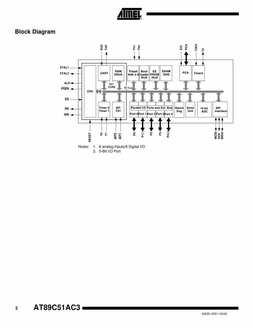
Block Diagram
Notes: 1. 8 analog Inputs/8 Digital I/O
2. 5-Bit I/O Port
Timer 0 INT
RAM256x8
T0
T1
RxD
Tx
D
WR
RD
EA
PSEN
ALE
XTAL2
XTAL1
UART
CPU
Timer 1
INT
1
Ctrl
INT
0
C51 CORE
Port 0
P0
Port 1 Port 2 Port 3
Parallel I/O Ports and Ext. Bus
P1(1
)
P2
P3
ERAM2048
IB-bus
PCA
RE
SE
T
WatchDog
PC
A
EC
I
Vs
s
Vc
c
Timer2
T2E
X
T2
Port 4
P4(2
)
EmulUnit
10 bitADC
Flash64k x 8
Bootloader2kx8
EEPROM2kx8
SPIInterface
MO
SI
SC
KM
ISO

3
AT89C51AC3
4383D–8051–02/08
Pin Configuration
PLCC44
P1
.3/A
N3
/CE
X0
P1
.2/A
N2
/EC
I
P1
.1/A
N1
/T2
EX
P1
.0/A
N 0
/T2
VA
RE
F
VA
GN
D
RE
SE
T
VS
S
VC
C
XT
AL
1
XT
AL
2
P3
.7/R
D
P4
.0
P4
.1
P2
.7/A
15
P2
.6/A
14
P2
.5/A
13
P2
.4/A
12
P2
.3/A
11
P2
.2/A
10
P2
.1/A
9
P3
.6/W
R
39
38
37
36
35
34
33
32
29
30
31
7
8
9
10
11
12
13
14
17
16
15
18
19
20
21
22
23
24
25
26
27
28
6 5 4 3 2
44
43
42
41
40
ALE
PSEN
P0.7/AD7
P0.6/AD6
P0.5/AD5
P0.2/AD2
P0.3/AD3
P0.4/AD4
P0.1/AD1
P0.0/AD0
P2.0/A8
P1.4/AN4/CEX1
P1.5/AN5/CEX2
P1.6/AN6/CEX3
P1.7/AN7/CEX4
EA
P3.0/RxD
P3.1/TxD
P3.2/INT0
P3.3/INT1
P3.4/T0
P3.5/T1
1
43 42 41 40 3944 38 37 36 35 34
12 13 17161514 201918 21 22
33
32
31
30
29
28
27
26
25
24
23
VQFP44
1
2
3
4
5
6
7
8
9
10
11
P1.4/AN4/CEX1
P1.5/AN5/CEX2
P1.6/AN6/CEX3
P1.7/AN7/CEX4
EA
P3.0/RxD
P3.1/TxD
P3.2/INT0
P3.3/INT1
P3.4/T0
P3.5/T1
ALE
PSEN
P0.7/AD7
P0.6/AD6
P0.5/AD5
P0.2 /AD2
P0.3 /AD3
P0.4 /AD4
P0.1 /AD1
P0.0 /AD0
P2.0/A8
P1
.3/A
N3
/CE
X0
P1
.2/A
N2
/EC
I
P1
.1/A
N1
/T2
EX
P1
.0/A
N 0
/T2
VA
RE
F
VA
GN
D
RE
SE
T
VS
S
VC
C
XT
AL
1
XT
AL
2
P3
.7/R
D
P4
.0
P4
.1
P2
.7/A
15
P2
.6/A
14
P2
.5/A
13
P2
.4/A
12
P2
.3/A
11
P2
.2/A
10
P2
.1/A
9
P3
.6/W
R
4 AT89C51AC34383D–8051–02/08
21 22 26252423 292827 30 31
5 4 3 2 1 6 52 51 50 49 48
8
9
10
11
12
13
14
15
16
17
18
46
45
44
43
42
41
40
39
38
37
36
PLCC52
7 47
19
20 32 33
34
35
P1
.3/A
N3
/CE
X0
P1
.2/A
N2
/EC
I
P1
.1/A
N1
/T2
EX
P1
.0/A
N 0
/T2
VA
RE
F
VA
GN
D
RE
SE
T
VS
S
VC
C
XT
AL
1
XT
AL
2
TE
ST
I
P1.4/AN4/CEX1
P1.5/AN5/CEX2
P1.6/AN6/CEX3
P1.7/AN7/CEX4
EA
P3.0/RxD
P3.1/TxD
P3.2/INT0
P3.3/INT1
P3.4/T0
P3.5/T1/SS
P4.3/SCK
ALE
PSEN
P0.7/AD7
P0.6/AD6
P0.5/AD5
P0.2 /AD2
P0.3 /AD3
P0.4 /AD4
P0.1 /AD1
P0.0 /AD0
P2.0/A8
P4.4/MOSI
P3
.7/R
D
P4
.0
P4
.1
P2
.7/A
15
P2
.6/A
14
P2
.5/A
13
P2
.4/A
12
P2
.3/A
11
P2
.2/A
10
P2
.1/A
9
P3
.6/W
R
P4
.2/M
ISO
NC
NC
NC
TESTI must be connected to VSS
VC
C54
53
52
51
50
49
VQFP64
P1
.3/A
N3
/CE
X0
P1
.2/A
N2
/EC
IP
1.1
/AN
1/T
2E
XP
1.0
/AN
0/T
2V
AR
EF
VA
GN
DR
ES
ET
VS
SV
SS
VS
S
P3
.7/R
DP
4.0
P4
.1P
2.7
/A1
5P
2.6
/A1
4N
CN
CN
CN
C
P3
.6/W
R
48
47
46
45
44
43
42
41
39
40
1
2
3
4
5
6
7
8
10
9
17
18
19
20
21
22
23
24
25
26
64
63
62
61
60
59
58
57
56
55
NCALEPSENP0.7/AD7P0.6/AD6
NCP0.5/AD5NC
NCP0.4/AD4
P1.4/AN4/CEX1NC
P1.5/AN5/CEX2P1.6/AN6/CEX3P1.7/AN7/CEX4
NCEANCNC
P3.0/RxD11
12
13
16
15
14
P4.3/SCKP3.1/TxD
P3.2/INT0P3.3/INT1
P3.4/T0P3.5/T1/SS
38
37
36
33
34
35
P0.1/AD1P0.2/AD2P0.3/AD3
P4.4/MOSIP0.0/AD0P2.0/A8
P2
.5/A
13
P2
.4/A
12
P2
.3/A
11
P2
.2/A
10
P2
.1/A
9P
4.2
/MIS
O
27
28
29
30
31
32
TE
ST
IV
CC
VC
C
XT
AL
1X
TA
L2
VC
C
TESTI must be connected to VSS

5
AT89C51AC3
4383D–8051–02/08
Pin Name Type Description
VSS GND Circuit ground
TESTI I Must be connected to VSS
VCC Supply Voltage
VAREF Reference Voltage for ADC
VAGND Reference Ground for ADC
P0.0:7 I/O Port 0:
Is an 8-bit open drain bi-directional I/O port. Port 0 pins that have 1’s written to them float, and in this state can be used as
high-impedance inputs. Port 0 is also the multiplexed low-order address and data bus during accesses to external Program
and Data Memory. In this application it uses strong internal pull-ups when emitting 1’s.
Port 0 also outputs the code Bytes during program validation. External pull-ups are required during program verification.
P1.0:7 I/O Port 1:
Is an 8-bit bi-directional I/O port with internal pull-ups. Port 1 pins can be used for digital input/output or as analog inputs for
the Analog Digital Converter (ADC). Port 1 pins that have 1’s written to them are pulled high by the internal pull-up transistors
and can be used as inputs in this state. As inputs, Port 1 pins that are being pulled low externally will be the source of current
(IIL, see section "Electrical Characteristic") because of the internal pull-ups. Port 1 pins are assigned to be used as analog
inputs via the ADCCF register (in this case the internal pull-ups are disconnected).
As a secondary digital function, port 1 contains the Timer 2 external trigger and clock input; the PCA external clock input and
the PCA module I/O.
P1.0/AN0/T2
Analog input channel 0,
External clock input for Timer/counter2.
P1.1/AN1/T2EX
Analog input channel 1,
Trigger input for Timer/counter2.
P1.2/AN2/ECI
Analog input channel 2,
PCA external clock input.
P1.3/AN3/CEX0
Analog input channel 3,
PCA module 0 Entry of input/PWM output.
P1.4/AN4/CEX1
Analog input channel 4,
PCA module 1 Entry of input/PWM output.
P1.5/AN5/CEX2
Analog input channel 5,
PCA module 2 Entry of input/PWM output.
P1.6/AN6/CEX3
Analog input channel 6,
PCA module 3 Entry of input/PWM output.
P1.7/AN7/CEX4
Analog input channel 7,
PCA module 4 Entry ot input/PWM output.
Port 1 receives the low-order address byte during EPROM programming and program verification.
It can drive CMOS inputs without external pull-ups.
P2.0:7 I/O Port 2:
Is an 8-bit bi-directional I/O port with internal pull-ups. Port 2 pins that have 1’s written to them are pulled high by the internal
pull-ups and can be used as inputs in this state. As inputs, Port 2 pins that are being pulled low externally will be a source of
current (IIL, see section "Electrical Characteristic") because of the internal pull-ups. Port 2 emits the high-order address byte
during accesses to the external Program Memory and during accesses to external Data Memory that uses 16-bit addresses
(MOVX @DPTR). In this application, it uses strong internal pull-ups when emitting 1’s. During accesses to external Data
Memory that use 8 bit addresses (MOVX @Ri), Port 2 transmits the contents of the P2 special function register.
It also receives high-order addresses and control signals during program validation.
It can drive CMOS inputs without external pull-ups.

6 AT89C51AC34383D–8051–02/08
P3.0:7 I/O Port 3:
Is an 8-bit bi-directional I/O port with internal pull-ups. Port 3 pins that have 1’s written to them are pulled high by the internal
pull-up transistors and can be used as inputs in this state. As inputs, Port 3 pins that are being pulled low externally will be a
source of current (IIL, see section "Electrical Characteristic") because of the internal pull-ups.
The output latch corresponding to a secondary function must be programmed to one for that function to operate (except for
TxD and WR). The secondary functions are assigned to the pins of port 3 as follows:
P3.0/RxD:
Receiver data input (asynchronous) or data input/output (synchronous) of the serial interface
P3.1/TxD:
Transmitter data output (asynchronous) or clock output (synchronous) of the serial interface
P3.2/INT0:
External interrupt 0 input/timer 0 gate control input
P3.3/INT1:
External interrupt 1 input/timer 1 gate control input
P3.4/T0:
Timer 0 counter input
P3.5/T1/SS:
Timer 1 counter input
SPI Slave Select
P3.6/WR:
External Data Memory write strobe; latches the data byte from port 0 into the external data memory
P3.7/RD:
External Data Memory read strobe; Enables the external data memory.
It can drive CMOS inputs without external pull-ups.
P4.0:4 I/O Port 4:
Is an 2-bit bi-directional I/O port with internal pull-ups. Port 4 pins that have 1’s written to them are pulled high by the internal
pull-ups and can be used as inputs in this state. As inputs, Port 4 pins that are being pulled low externally will be a source of
current (IIL, on the datasheet) because of the internal pull-up transistor.
The secondary functions are assigned to the 5 pins of port 4 as follows:
P4.0: Regular Port I/O
P4.1: Regular Port I/O
P4.2/MISO:
Master Input Slave Output of SPI controller
P4.3/SCK:
Serial Clock of SPI controller
P4.4/MOSI:
Master Ouput Slave Input of SPI controller
It can drive CMOS inputs without external pull-ups.
Pin Name Type Description
7
AT89C51AC3
4383D–8051–02/08
I/O Configurations Each Port SFR operates via type-D latches, as illustrated in Figure 1 for Ports 3 and 4. A
CPU "write to latch" signal initiates transfer of internal bus data into the type-D latch. A
CPU "read latch" signal transfers the latched Q output onto the internal bus. Similarly, a
"read pin" signal transfers the logical level of the Port pin. Some Port data instructions
activate the "read latch" signal while others activate the "read pin" signal. Latch instruc-
tions are referred to as Read-Modify-Write instructions. Each I/O line may be
independently programmed as input or output.
Port 1, Port 3 and Port 4 Figure 1 shows the structure of Ports 1 and 3, which have internal pull-ups. An external
source can pull the pin low. Each Port pin can be configured either for general-purpose
I/O or for its alternate input output function.
To use a pin for general-purpose output, set or clear the corresponding bit in the Px reg-
ister (x = 1,3 or 4). To use a pin for general-purpose input, set the bit in the Px register.
This turns off the output FET drive.
To configure a pin for its alternate function, set the bit in the Px register. When the latch
is set, the "alternate output function" signal controls the output level (see Figure 1). The
operation of Ports 1, 3 and 4 is discussed further in the "quasi-Bidirectional Port Opera-
tion" section.
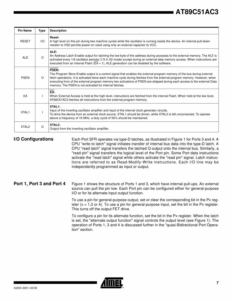
RESET I/O
Reset:
A high level on this pin during two machine cycles while the oscillator is running resets the device. An internal pull-down
resistor to VSS permits power-on reset using only an external capacitor to VCC.
ALE O
ALE:
An Address Latch Enable output for latching the low byte of the address during accesses to the external memory. The ALE is
activated every 1/6 oscillator periods (1/3 in X2 mode) except during an external data memory access. When instructions are
executed from an internal Flash (EA = 1), ALE generation can be disabled by the software.
PSEN O
PSEN:
The Program Store Enable output is a control signal that enables the external program memory of the bus during external
fetch operations. It is activated twice each machine cycle during fetches from the external program memory. However, when
executing from of the external program memory two activations of PSEN are skipped during each access to the external Data
memory. The PSEN is not activated for internal fetches.
EA I
EA:
When External Access is held at the high level, instructions are fetched from the internal Flash. When held at the low level,
AT89C51AC3 fetches all instructions from the external program memory.
XTAL1 I
XTAL1:
Input of the inverting oscillator amplifier and input of the internal clock generator circuits.
To drive the device from an external clock source, XTAL1 should be driven, while XTAL2 is left unconnected. To operate
above a frequency of 16 MHz, a duty cycle of 50% should be maintained.
XTAL2 OXTAL2:
Output from the inverting oscillator amplifier.
Pin Name Type Description

8 AT89C51AC34383D–8051–02/08
Figure 1. Port 1, Port 3 and Port 4 Structure
Note: The internal pull-up can be disabled on P1 when analog function is selected.
Port 0 and Port 2 Ports 0 and 2 are used for general-purpose I/O or as the external address/data bus. Port
0, shown in Figure 3, differs from the other Ports in not having internal pull-ups. Figure 3
shows the structure of Port 2. An external source can pull a Port 2 pin low.
To use a pin for general-purpose output, set or clear the corresponding bit in the Px reg-
ister (x = 0 or 2). To use a pin for general-purpose input, set the bit in the Px register to
turn off the output driver FET.
Figure 2. Port 0 Structure
Notes: 1. Port 0 is precluded from use as general-purpose I/O Ports when used as
address/data bus drivers.
2. Port 0 internal strong pull-ups assist the logic-one output for memory bus cycles only.
Except for these bus cycles, the pull-up FET is off, Port 0 outputs are open-drain.
D
CL
QP1.X
LATCH
INTERNAL
WRITETOLATCH
READPIN
READLATCH
P1.x
P3.XP4.X
ALTERNATEOUTPUTFUNCTION
VCC
INTERNALPULL-UP (1)
ALTERNATEINPUTFUNCTION
P3.xP4.x
BUS
D QP0.X
LATCH
INTERNAL
WRITETOLATCH
READPIN
READLATCH
0
1
P0.x (1)
ADDRESS LOW/DATA
CONTROL VDD
BUS
(2)
9
AT89C51AC3
4383D–8051–02/08
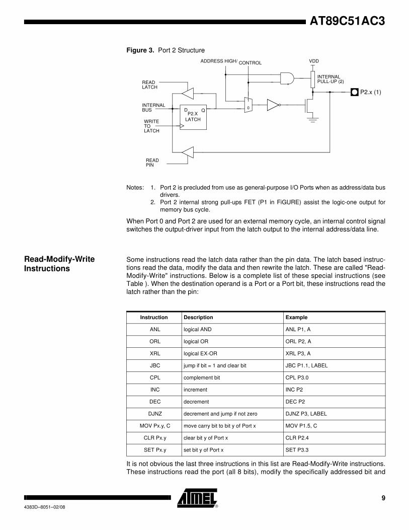
Figure 3. Port 2 Structure
Notes: 1. Port 2 is precluded from use as general-purpose I/O Ports when as address/data bus
drivers.
2. Port 2 internal strong pull-ups FET (P1 in FiGURE) assist the logic-one output for
memory bus cycle.
When Port 0 and Port 2 are used for an external memory cycle, an internal control signal
switches the output-driver input from the latch output to the internal address/data line.
Read-Modify-Write Instructions
Some instructions read the latch data rather than the pin data. The latch based instruc-
tions read the data, modify the data and then rewrite the latch. These are called "Read-
Modify-Write" instructions. Below is a complete list of these special instructions (see
Table ). When the destination operand is a Port or a Port bit, these instructions read the
latch rather than the pin:
It is not obvious the last three instructions in this list are Read-Modify-Write instructions.
These instructions read the port (all 8 bits), modify the specifically addressed bit and
D QP2.X
LATCH
INTERNAL
WRITETOLATCH
READPIN
READLATCH
0
1
P2.x (1)
ADDRESS HIGH/ CONTROL
BUS
VDD
INTERNALPULL-UP (2)
Instruction Description Example
ANL logical AND ANL P1, A
ORL logical OR ORL P2, A
XRL logical EX-OR XRL P3, A
JBC jump if bit = 1 and clear bit JBC P1.1, LABEL
CPL complement bit CPL P3.0
INC increment INC P2
DEC decrement DEC P2
DJNZ decrement and jump if not zero DJNZ P3, LABEL
MOV Px.y, C move carry bit to bit y of Port x MOV P1.5, C
CLR Px.y clear bit y of Port x CLR P2.4
SET Px.y set bit y of Port x SET P3.3

10 AT89C51AC34383D–8051–02/08
write the new byte back to the latch. These Read-Modify-Write instructions are directed
to the latch rather than the pin in order to avoid possible misinterpretation of voltage
(and therefore, logic) levels at the pin. For example, a Port bit used to drive the base of
an external bipolar transistor can not rise above the transistor’s base-emitter junction
voltage (a value lower than VIL). With a logic one written to the bit, attempts by the CPU
to read the Port at the pin are misinterpreted as logic zero. A read of the latch rather
than the pins returns the correct logic-one value.
Quasi-Bidirectional Port Operation
Port 1, Port 2, Port 3 and Port 4 have fixed internal pull-ups and are referred to as
"quasi-bidirectional" Ports. When configured as an input, the pin impedance appears as
logic one and sources current in response to an external logic zero condition. Port 0 is a
"true bidirectional" pin. The pins float when configured as input. Resets write logic one to
all Port latches. If logical zero is subsequently written to a Port latch, it can be returned
to input conditions by a logical one written to the latch.
Note: Port latch values change near the end of Read-Modify-Write instruction cycles. Output
buffers (and therefore the pin state) update early in the instruction after Read-Modify-
Write instruction cycle.
Logical zero-to-one transitions in Port 1, Port 2, Port 3 and Port 4 use an additional pull-
up (p1) to aid this logic transition (see Figure 4.). This increases switch speed. This
extra pull-up sources 100 times normal internal circuit current during 2 oscillator clock
periods. The internal pull-ups are field-effect transistors rather than linear resistors. Pull-
ups consist of three p-channel FET (pFET) devices. A pFET is on when the gate senses
logical zero and off when the gate senses logical one. pFET #1 is turned on for two
oscillator periods immediately after a zero-to-one transition in the Port latch. A logical
one at the Port pin turns on pFET #3 (a weak pull-up) through the inverter. This inverter
and pFET pair form a latch to drive logical one. pFET #2 is a very weak pull-up switched
on whenever the associated nFET is switched off. This is traditional CMOS switch con-
vention. Current strengths are 1/10 that of pFET #3.
Figure 4. Internal Pull-Up Configurations
Note: Port 2 p1 assists the logic-one output for memory bus cycles.
READ PIN
INPUT DATA
P1.x
OUTPUT DATA
2 Osc. PERIODS
n
p1(1) p2 p3
VCCVCCVCC
P2.xP3.xP4.x

11
AT89C51AC3
4383D–8051–02/08
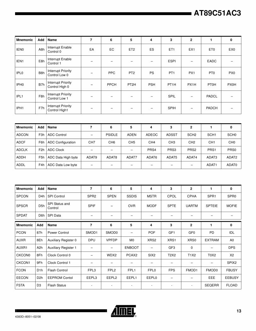
SFR Mapping The Special Function Registers (SFRs) of the AT89C51AC3 fall into the following
categories:
Mnemonic Add Name 7 6 5 4 3 2 1 0
ACC E0h Accumulator – – – – – – – –
B F0h B Register – – – – – – – –
PSW D0h Program Status Word CY AC F0 RS1 RS0 OV F1 P
SP 81h Stack Pointer – – – – – – – –
DPL 82h
Data Pointer Low
byte
LSB of DPTR
– – – – – – – –
DPH 83h
Data Pointer High
byte
MSB of DPTR
– – – – – – – –
Mnemonic Add Name 7 6 5 4 3 2 1 0
P0 80h Port 0 – – – – – – – –
P1 90h Port 1 – – – – – – – –
P2 A0h Port 2 – – – – – – – –
P3 B0h Port 3 – – – – – – – –
P4 C0h Port 4 (x5) – – –P4.4 /
MOSI
P4.3 /
SCK
P4.2 /
MISOP4.1 P4.0
Mnemonic Add Name 7 6 5 4 3 2 1 0
TH0 8ChTimer/Counter 0 High
byte– – – – – – – –
TL0 8AhTimer/Counter 0 Low
byte– – – – – – – –
TH1 8DhTimer/Counter 1 High
byte– – – – – – – –
TL1 8BhTimer/Counter 1 Low
byte– – – – – – – –
TH2 CDhTimer/Counter 2 High
byte– – – – – – – –
TL2 CChTimer/Counter 2 Low
byte– – – – – – – –
TCON 88hTimer/Counter 0 and
1 controlTF1 TR1 TF0 TR0 IE1 IT1 IE0 IT0
TMOD 89hTimer/Counter 0 and
1 ModesGATE1 C/T1# M11 M01 GATE0 C/T0# M10 M00

12 AT89C51AC34383D–8051–02/08
T2CON C8hTimer/Counter 2
controlTF2 EXF2 RCLK TCLK EXEN2 TR2 C/T2# CP/RL2#
T2MOD C9hTimer/Counter 2
Mode– – – – – – T2OE DCEN
RCAP2H CBh
Timer/Counter 2
Reload/Capture High
byte
– – – – – – – –
RCAP2L CAh
Timer/Counter 2
Reload/Capture Low
byte
– – – – – – – –
WDTRST A6hWatchDog Timer
Reset– – – – – – – –
WDTPRG A7hWatchDog Timer
Program– – – – – S2 S1 S0
Mnemonic Add Name 7 6 5 4 3 2 1 0
Mnemonic Add Name 7 6 5 4 3 2 1 0
SCON 98h Serial Control FE/SM0 SM1 SM2 REN TB8 RB8 TI RI
SBUF 99h Serial Data Buffer – – – – – – – –
SADEN B9h Slave Address Mask – – – – – – – –
SADDR A9h Slave Address – – – – – – – –
Mnemonic Add Name 7 6 5 4 3 2 1 0
CCON D8h PCA Timer/Counter Control CF CR – CCF4 CCF3 CCF2 CCF1 CCF0
CMOD D9h PCA Timer/Counter Mode CIDL WDTE – – – CPS1 CPS0 ECF
CL E9h PCA Timer/Counter Low byte – – – – – – – –
CH F9h PCA Timer/Counter High byte – – – – – – – –
CCAPM0
CCAPM1
CCAPM2
CCAPM3
CCAPM4
DAh
DBh
DCh
DDh
DEh
PCA Timer/Counter Mode 0
PCA Timer/Counter Mode 1
PCA Timer/Counter Mode 2
PCA Timer/Counter Mode 3
PCA Timer/Counter Mode 4
–
ECOM0
ECOM1
ECOM2
ECOM3
ECOM4
CAPP0
CAPP1
CAPP2
CAPP3
CAPP4
CAPN0
CAPN1
CAPN2
CAPN3
CAPN4
MAT0
MAT1
MAT2
MAT3
MAT4
TOG0
TOG1
TOG2
TOG3
TOG4
PWM0
PWM1
PWM2
PWM3
PWM4
ECCF0
ECCF1
ECCF2
ECCF3
ECCF4
CCAP0H
CCAP1H
CCAP2H
CCAP3H
CCAP4H
FAh
FBh
FCh
FDh
FEh
PCA Compare Capture Module 0 H
PCA Compare Capture Module 1 H
PCA Compare Capture Module 2 H
PCA Compare Capture Module 3 H
PCA Compare Capture Module 4 H
CCAP0H7
CCAP1H7
CCAP2H7
CCAP3H7
CCAP4H7
CCAP0H6
CCAP1H6
CCAP2H6
CCAP3H6
CCAP4H6
CCAP0H5
CCAP1H5
CCAP2H5
CCAP3H5
CCAP4H5
CCAP0H4
CCAP1H4
CCAP2H4
CCAP3H4
CCAP4H4
CCAP0H3
CCAP1H3
CCAP2H3
CCAP3H3
CCAP4H3
CCAP0H2
CCAP1H2
CCAP2H2
CCAP3H2
CCAP4H2
CCAP0H1
CCAP1H1
CCAP2H1
CCAP3H1
CCAP4H1
CCAP0H0
CCAP1H0
CCAP2H0
CCAP3H0
CCAP4H0
CCAP0L
CCAP1L
CCAP2L
CCAP3L
CCAP4L
EAh
EBh
ECh
EDh
EEh
PCA Compare Capture Module 0 L
PCA Compare Capture Module 1 L
PCA Compare Capture Module 2 L
PCA Compare Capture Module 3 L
PCA Compare Capture Module 4 L
CCAP0L7
CCAP1L7
CCAP2L7
CCAP3L7
CCAP4L7
CCAP0L6
CCAP1L6
CCAP2L6
CCAP3L6
CCAP4L6
CCAP0L5
CCAP1L5
CCAP2L5
CCAP3L5
CCAP4L5
CCAP0L4
CCAP1L4
CCAP2L4
CCAP3L4
CCAP4L4
CCAP0L3
CCAP1L3
CCAP2L3
CCAP3L3
CCAP4L3
CCAP0L2
CCAP1L2
CCAP2L2
CCAP3L2
CCAP4L2
CCAP0L1
CCAP1L1
CCAP2L1
CCAP3L1
CCAP4L1
CCAP0L0
CCAP1L0
CCAP2L0
CCAP3L0
CCAP4L0
13
AT89C51AC3
4383D–8051–02/08
Mnemonic Add Name 7 6 5 4 3 2 1 0
IEN0 A8hInterrupt Enable
Control 0EA EC ET2 ES ET1 EX1 ET0 EX0
IEN1 E8hInterrupt Enable
Control 1– – – – ESPI – EADC –
IPL0 B8hInterrupt Priority
Control Low 0– PPC PT2 PS PT1 PX1 PT0 PX0
IPH0 B7hInterrupt Priority
Control High 0– PPCH PT2H PSH PT1H PX1H PT0H PX0H
IPL1 F8hInterrupt Priority
Control Low 1– – – – SPIL – PADCL –
IPH1 F7hInterrupt Priority
Control High1– – – – SPIH – PADCH –
Mnemonic Add Name 7 6 5 4 3 2 1 0
ADCON F3h ADC Control – PSIDLE ADEN ADEOC ADSST SCH2 SCH1 SCH0
ADCF F6h ADC Configuration CH7 CH6 CH5 CH4 CH3 CH2 CH1 CH0
ADCLK F2h ADC Clock – – – PRS4 PRS3 PRS2 PRS1 PRS0
ADDH F5h ADC Data High byte ADAT9 ADAT8 ADAT7 ADAT6 ADAT5 ADAT4 ADAT3 ADAT2
ADDL F4h ADC Data Low byte – – – – – – ADAT1 ADAT0
Mnemonic Add Name 7 6 5 4 3 2 1 0
SPCON D4h SPI Control SPR2 SPEN SSDIS MSTR CPOL CPHA SPR1 SPR0
SPSCR D5hSPI Status and
ControlSPIF – OVR MODF SPTE UARTM SPTEIE MOFIE
SPDAT D6h SPI Data – – – – – – – –
Mnemonic Add Name 7 6 5 4 3 2 1 0
PCON 87h Power Control SMOD1 SMOD0 – POF GF1 GF0 PD IDL
AUXR 8Eh Auxiliary Register 0 DPU VPFDP M0 XRS2 XRS1 XRS0 EXTRAM A0
AUXR1 A2h Auxiliary Register 1 – – ENBOOT – GF3 0 – DPS
CKCON0 8Fh Clock Control 0 – WDX2 PCAX2 SIX2 T2X2 T1X2 T0X2 X2
CKCON1 9Fh Clock Control 1 – – – – – – – SPIX2
FCON D1h Flash Control FPL3 FPL2 FPL1 FPL0 FPS FMOD1 FMOD0 FBUSY
EECON D2h EEPROM Contol EEPL3 EEPL2 EEPL1 EEPL0 – – EEE EEBUSY
FSTA D3 Flash Status - - - - - - SEQERR FLOAD
14 AT89C51AC34383D–8051–02/08
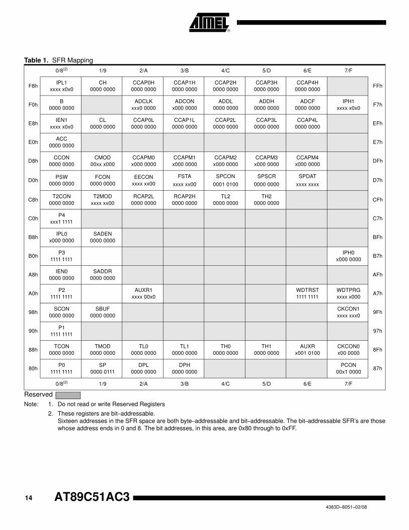
Reserved
Note: 1. Do not read or write Reserved Registers
2. These registers are bit–addressable.
Sixteen addresses in the SFR space are both byte–addressable and bit–addressable. The bit–addressable SFR’s are those
whose address ends in 0 and 8. The bit addresses, in this area, are 0x80 through to 0xFF.
Table 1. SFR Mapping
0/8(2) 1/9 2/A 3/B 4/C 5/D 6/E 7/F
F8hIPL1
xxxx x0x0
CH
0000 0000
CCAP0H
0000 0000
CCAP1H
0000 0000
CCAP2H
0000 0000
CCAP3H
0000 0000
CCAP4H
0000 0000FFh
F0hB
0000 0000
ADCLK
xxx0 0000
ADCON
x000 0000
ADDL
0000 0000
ADDH
0000 0000
ADCF
0000 0000
IPH1
xxxx x0x0F7h
E8hIEN1
xxxx x0x0
CL
0000 0000
CCAP0L
0000 0000
CCAP1L
0000 0000
CCAP2L
0000 0000
CCAP3L
0000 0000
CCAP4L
0000 0000EFh
E0hACC
0000 0000E7h
D8hCCON
0000 0000
CMOD
00xx x000
CCAPM0
x000 0000
CCAPM1
x000 0000
CCAPM2
x000 0000
CCAPM3
x000 0000
CCAPM4
x000 0000DFh
D0hPSW
0000 0000
FCON
0000 0000
EECON
xxxx xx00
FSTA
xxxx xx00
SPCON
0001 0100
SPSCR
0000 0000
SPDAT
xxxx xxxxD7h
C8hT2CON
0000 0000
T2MOD
xxxx xx00
RCAP2L
0000 0000
RCAP2H
0000 0000
TL2
0000 0000
TH2
0000 0000CFh
C0hP4
xxx1 1111C7h
B8hIPL0
x000 0000
SADEN
0000 0000BFh
B0hP3
1111 1111
IPH0
x000 0000B7h
A8hIEN0
0000 0000
SADDR
0000 0000AFh
A0hP2
1111 1111
AUXR1
xxxx 00x0
WDTRST
1111 1111
WDTPRG
xxxx x000A7h
98hSCON
0000 0000
SBUF
0000 0000
CKCON1
xxxx xxx09Fh
90hP1
1111 111197h
88hTCON
0000 0000
TMOD
0000 0000
TL0
0000 0000
TL1
0000 0000
TH0
0000 0000
TH1
0000 0000
AUXR
x001 0100
CKCON0
x00 00008Fh
80hP0
1111 1111
SP
0000 0111
DPL
0000 0000
DPH
0000 0000
PCON
00x1 000087h
0/8(2) 1/9 2/A 3/B 4/C 5/D 6/E 7/F

15
AT89C51AC3
4383D–8051–02/08
Clock The AT89C51AC3 core needs only 6 clock periods per machine cycle. This feature,
called”X2”, provides the following advantages:
• Divides frequency crystals by 2 (cheaper crystals) while keeping the same CPU
power.
• Saves power consumption while keeping the same CPU power (oscillator power
saving).
• Saves power consumption by dividing dynamic operating frequency by 2 in
operating and idle modes.
• Increases CPU power by 2 while keeping the same crystal frequency.
In order to keep the original C51 compatibility, a divider-by-2 is inserted between the
XTAL1 signal and the main clock input of the core (phase generator). This divider may
be disabled by the software.
An extra feature is available to start after Reset in the X2 mode. This feature can be
enabled by a bit X2B in the Hardware Security Byte. This bit is described in the section
"In-System Programming".
Description The X2 bit in the CKCON register (see Table 2) allows switching from 12 clock cycles
per instruction to 6 clock cycles and vice versa. At reset, the standard speed is activated
(STD mode).
Setting this bit activates the X2 feature (X2 mode) for the CPU Clock only (see Figure
5.).
The Timers 0, 1 and 2, Uart, PCA or WatchDog switch in X2 mode only if the corre-
sponding bit is cleared in the CKCON register.
The clock for the whole circuit and peripheral is first divided by two before being used by
the CPU core and peripherals. This allows any cyclic ratio to be accepted on the XTAL1
input. In X2 mode, as this divider is bypassed, the signals on XTAL1 must have a cyclic
ratio between 40 to 60%. Figure 5. shows the clock generation block diagram. The X2
bit is validated on the XTAL1÷2 rising edge to avoid glitches when switching from the X2
to the STD mode. Figure 6 shows the mode switching waveforms.

16 AT89C51AC34383D–8051–02/08
Figure 5. Clock CPU Generation Diagram
XTAL1
XTAL2
PDPCON.1
CPU Core
1
0÷ 2
PERIPHCLOCK
Clock
Peripheral
CPUCLOCK
CPU Core Clock Symbol
X2CKCON.0
X2BHardware byte
WDX2CKCON0.6
PCAX2CKCON0.5
SIX2CKCON0.4
T2X2CKCON0.3
T1X2CKCON0.2
T0X2CKCON0.1
IDLPCON.0
1
0
÷ 2
1
0
÷ 2
1
0
÷ 2
1
0
÷ 2
1
0
÷ 2
1
0
÷ 2
X2CKCON.0
FWd Clock
FPca Clock
FUart Clock
FT2 Clock
FT1 Clock
FT0 Clock
and ADC
On RESET
1
0
÷ 2FSPIClock
SPIX2CKCON1.0 Clock Symbol

17
AT89C51AC3
4383D–8051–02/08
Figure 6. Mode Switching Waveforms
Note: In order to prevent any incorrect operation while operating in the X2 mode, users must be aware that all peripherals using the
clock frequency as a time reference (UART, timers...) will have their time reference divided by two. For example a free running
timer generating an interrupt every 20 ms will then generate an interrupt every 10 ms. A UART with a 4800 baud rate will have
a 9600 baud rate.
XTAL1/2
XTAL1
CPU clock
X2 bit
X2 ModeSTD Mode STD Mode
18 AT89C51AC34383D–8051–02/08
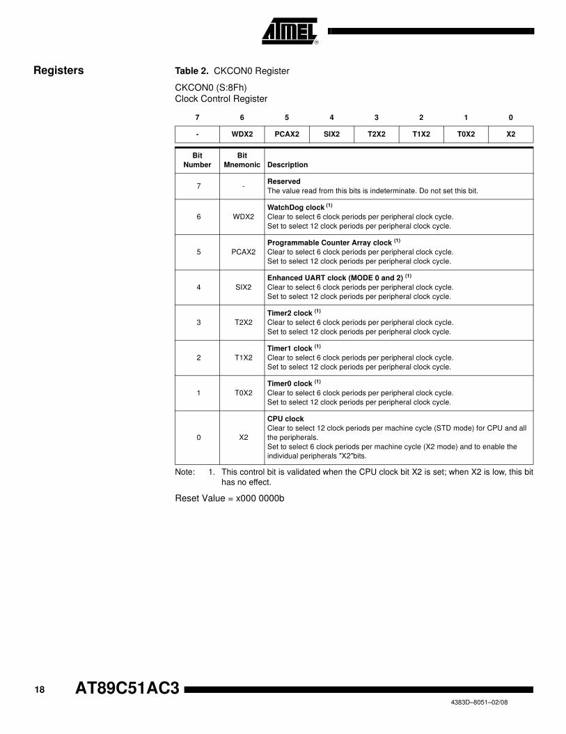
Registers Table 2. CKCON0 Register
CKCON0 (S:8Fh)
Clock Control Register
Note: 1. This control bit is validated when the CPU clock bit X2 is set; when X2 is low, this bit
has no effect.
Reset Value = x000 0000b
7 6 5 4 3 2 1 0
- WDX2 PCAX2 SIX2 T2X2 T1X2 T0X2 X2
Bit
Number
Bit
Mnemonic Description
7 -Reserved
The value read from this bits is indeterminate. Do not set this bit.
6 WDX2
WatchDog clock (1)
Clear to select 6 clock periods per peripheral clock cycle.
Set to select 12 clock periods per peripheral clock cycle.
5 PCAX2
Programmable Counter Array clock (1)
Clear to select 6 clock periods per peripheral clock cycle.
Set to select 12 clock periods per peripheral clock cycle.
4 SIX2
Enhanced UART clock (MODE 0 and 2) (1)
Clear to select 6 clock periods per peripheral clock cycle.
Set to select 12 clock periods per peripheral clock cycle.
3 T2X2
Timer2 clock (1)
Clear to select 6 clock periods per peripheral clock cycle.
Set to select 12 clock periods per peripheral clock cycle.
2 T1X2
Timer1 clock (1)
Clear to select 6 clock periods per peripheral clock cycle.
Set to select 12 clock periods per peripheral clock cycle.
1 T0X2
Timer0 clock (1)
Clear to select 6 clock periods per peripheral clock cycle.
Set to select 12 clock periods per peripheral clock cycle.
0 X2
CPU clock
Clear to select 12 clock periods per machine cycle (STD mode) for CPU and all
the peripherals.
Set to select 6 clock periods per machine cycle (X2 mode) and to enable the
individual peripherals "X2"bits.
19
AT89C51AC3
4383D–8051–02/08
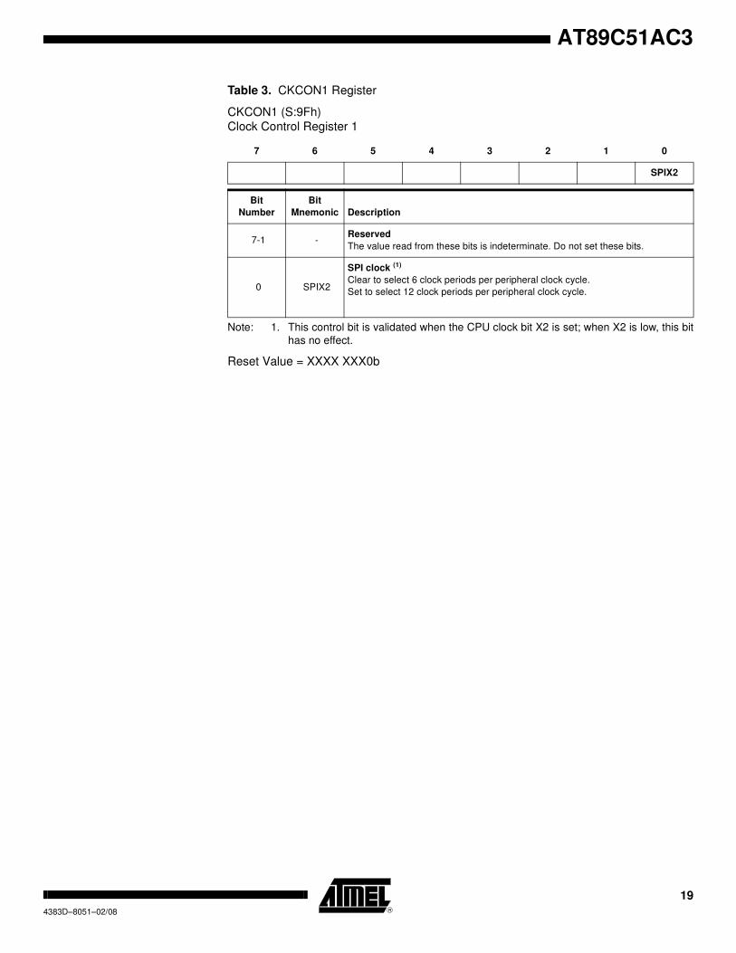
Table 3. CKCON1 Register
CKCON1 (S:9Fh)
Clock Control Register 1
Note: 1. This control bit is validated when the CPU clock bit X2 is set; when X2 is low, this bit
has no effect.
Reset Value = XXXX XXX0b
7 6 5 4 3 2 1 0
SPIX2
Bit
Number
Bit
Mnemonic Description
7-1 -Reserved
The value read from these bits is indeterminate. Do not set these bits.
0 SPIX2
SPI clock (1)
Clear to select 6 clock periods per peripheral clock cycle.
Set to select 12 clock periods per peripheral clock cycle.
20 AT89C51AC34383D–8051–02/08
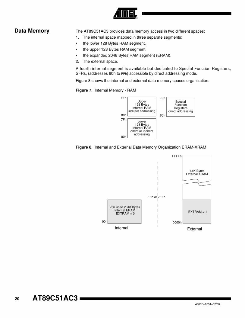
Data Memory The AT89C51AC3 provides data memory access in two different spaces:
1. The internal space mapped in three separate segments:
• the lower 128 Bytes RAM segment.
• the upper 128 Bytes RAM segment.
• the expanded 2048 Bytes RAM segment (ERAM).
2. The external space.
A fourth internal segment is available but dedicated to Special Function Registers,
SFRs, (addresses 80h to FFh) accessible by direct addressing mode.
Figure 8 shows the internal and external data memory spaces organization.
Figure 7. Internal Memory - RAM
Figure 8. Internal and External Data Memory Organization ERAM-XRAM
Upper128 Bytes
Internal RAM
Lower128 Bytes
Internal RAM
SpecialFunctionRegisters
80h 80h
00h
FFh FFh
direct addressing
addressing
7Fh
direct or indirect
indirect addressing
256 up to 2048 Bytes
00h
64K BytesExternal XRAM
0000h
FFFFh
Internal ERAMEXTRAM = 0
EXTRAM = 1
FFh or 7FFh
Internal External
21
AT89C51AC3
4383D–8051–02/08
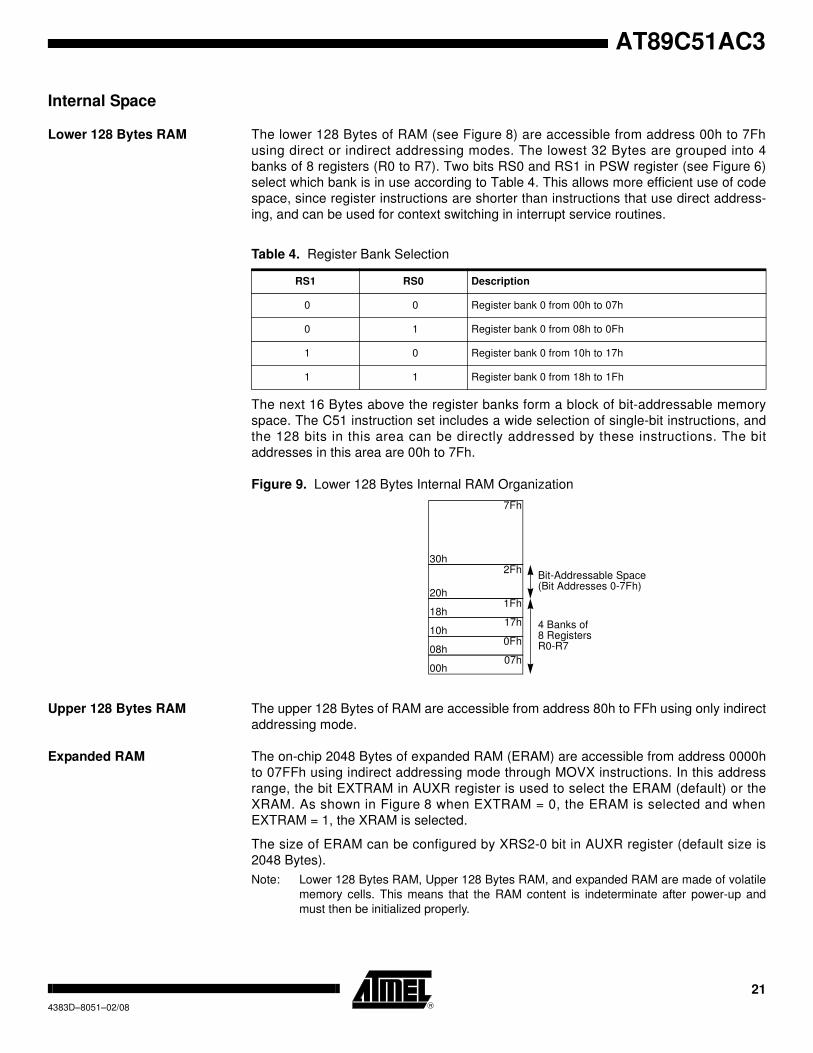
Internal Space
Lower 128 Bytes RAM The lower 128 Bytes of RAM (see Figure 8) are accessible from address 00h to 7Fh
using direct or indirect addressing modes. The lowest 32 Bytes are grouped into 4
banks of 8 registers (R0 to R7). Two bits RS0 and RS1 in PSW register (see Figure 6)
select which bank is in use according to Table 4. This allows more efficient use of code
space, since register instructions are shorter than instructions that use direct address-
ing, and can be used for context switching in interrupt service routines.
Table 4. Register Bank Selection
The next 16 Bytes above the register banks form a block of bit-addressable memory
space. The C51 instruction set includes a wide selection of single-bit instructions, and
the 128 bits in this area can be directly addressed by these instructions. The bit
addresses in this area are 00h to 7Fh.
Figure 9. Lower 128 Bytes Internal RAM Organization
Upper 128 Bytes RAM The upper 128 Bytes of RAM are accessible from address 80h to FFh using only indirect
addressing mode.
Expanded RAM The on-chip 2048 Bytes of expanded RAM (ERAM) are accessible from address 0000h
to 07FFh using indirect addressing mode through MOVX instructions. In this address
range, the bit EXTRAM in AUXR register is used to select the ERAM (default) or the
XRAM. As shown in Figure 8 when EXTRAM = 0, the ERAM is selected and when
EXTRAM = 1, the XRAM is selected.
The size of ERAM can be configured by XRS2-0 bit in AUXR register (default size is
2048 Bytes).
Note: Lower 128 Bytes RAM, Upper 128 Bytes RAM, and expanded RAM are made of volatile
memory cells. This means that the RAM content is indeterminate after power-up and
must then be initialized properly.
RS1 RS0 Description
0 0 Register bank 0 from 00h to 07h
0 1 Register bank 0 from 08h to 0Fh
1 0 Register bank 0 from 10h to 17h
1 1 Register bank 0 from 18h to 1Fh
Bit-Addressable Space
4 Banks of 8 RegistersR0-R7
30h
7Fh
(Bit Addresses 0-7Fh)20h
2Fh
18h1Fh
10h17h
08h0Fh
00h07h

22 AT89C51AC34383D–8051–02/08
External Space
Memory Interface The external memory interface comprises the external bus (port 0 and port 2) as well as
the bus control signals (RD#, WR#, and ALE).
Figure 10 shows the structure of the external address bus. P0 carries address A7:0
while P2 carries address A15:8. Data D7:0 is multiplexed with A7:0 on P0. Table 5
describes the external memory interface signals.
Figure 10. External Data Memory Interface Structure
Table 5. External Data Memory Interface Signals
External Bus Cycles This section describes the bus cycles the AT89C51AC3 executes to read (see
Figure 11), and write data (see Figure 12) in the external data memory.
External memory cycle takes 6 CPU clock periods. This is equivalent to 12 oscillator
clock period in standard mode or 6 oscillator clock periods in X2 mode. For further infor-
mation on X2 mode.
Slow peripherals can be accessed by stretching the read and write cycles. This is done
using the M0 bit in AUXR register. Setting this bit changes the width of the RD# and
WR# signals from 3 to 15 CPU clock periods.
For simplicity, the accompanying figures depict the bus cycle waveforms in idealized
form and do not provide precise timing information. For bus cycle timing parameters
refer to the Section “AC Characteristics” of the AT89C51AC3 datasheet.
Signal
Name Type Description
Alternative
Function
A15:8 OAddress Lines
Upper address lines for the external bus.P2.7:0
AD7:0 I/O
Address/Data Lines
Multiplexed lower address lines and data for the external
memory.
P0.7:0
ALE O
Address Latch Enable
ALE signals indicates that valid address information are available
on lines AD7:0.
-
RD# ORead
Read signal output to external data memory.P3.7
WR# OWrite
Write signal output to external memory.P3.6
RAM
PERIPHERALAT89C51AC3
P2
P0AD7:0
A15:8
A7:0
A15:8
D7:0
A7:0
ALE
WR
OERD#
WR#
Latch

23
AT89C51AC3
4383D–8051–02/08
Figure 11. External Data Read Waveforms
Notes: 1. RD# signal may be stretched using M0 bit in AUXR register.
2. When executing MOVX @Ri instruction, P2 outputs SFR content.
Figure 12. External Data Write Waveforms
Notes: 1. WR# signal may be stretched using M0 bit in AUXR register.
2. When executing MOVX @Ri instruction, P2 outputs SFR content.
ALE
P0
P2
RD#1
DPL or Ri D7:0
DPH or P22P2
CPU Clock
ALE
P0
P2
WR#1
DPL or Ri D7:0
P2
CPU Clock
DPH or P22

24 AT89C51AC34383D–8051–02/08
Dual Data Pointer
Description The AT89C51AC3 implements a second data pointer for speeding up code execution
and reducing code size in case of intensive usage of external memory accesses.
DPTR 0 and DPTR 1 are seen by the CPU as DPTR and are accessed using the SFR
addresses 83h and 84h that are the DPH and DPL addresses. The DPS bit in AUXR1
register (see Figure 8) is used to select whether DPTR is the data pointer 0 or the data
pointer 1 (see Figure 13).
Figure 13. Dual Data Pointer Implementation
Application Software can take advantage of the additional data pointers to both increase speed and
reduce code size, for example, block operations (copy, compare…) are well served by
using one data pointer as a “source” pointer and the other one as a “destination” pointer.
Hereafter is an example of block move implementation using the two pointers and coded
in assembler. The latest C compiler takes also advantage of this feature by providing
enhanced algorithm libraries.
The INC instruction is a short (2 Bytes) and fast (6 machine cycle) way to manipulate the
DPS bit in the AUXR1 register. However, note that the INC instruction does not directly
force the DPS bit to a particular state, but simply toggles it. In simple routines, such as
the block move example, only the fact that DPS is toggled in the proper sequence mat-
ters, not its actual value. In other words, the block move routine works the same whether
DPS is '0' or '1' on entry.; ASCII block move using dual data pointers
; Modifies DPTR0, DPTR1, A and PSW
; Ends when encountering NULL character
; Note: DPS exits opposite to the entry state unless an extra INC AUXR1 is added
AUXR1EQU0A2h
move:movDPTR,#SOURCE ; address of SOURCE
incAUXR1 ; switch data pointers
movDPTR,#DEST ; address of DEST
mv_loop:incAUXR1; switch data pointers
movxA,@DPTR; get a byte from SOURCE
incDPTR; increment SOURCE address
incAUXR1; switch data pointers
movx@DPTR,A; write the byte to DEST
incDPTR; increment DEST address
jnzmv_loop; check for NULL terminator
end_move:
0
1
DPH0
DPH1
DPL0
0
1
DPS AUXR1.0
DPH
DPLDPL1
DPTRDPTR0
DPTR1
25
AT89C51AC3
4383D–8051–02/08
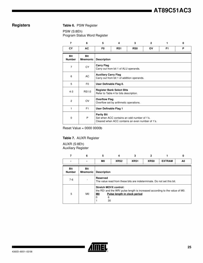
Registers Table 6. PSW Register
PSW (S:8Eh)
Program Status Word Register
Reset Value = 0000 0000b
Table 7. AUXR Register
AUXR (S:8Eh)
Auxiliary Register
7 6 5 4 3 2 1 0
CY AC F0 RS1 RS0 OV F1 P
Bit
Number
Bit
Mnemonic Description
7 CYCarry Flag
Carry out from bit 1 of ALU operands.
6 ACAuxiliary Carry Flag
Carry out from bit 1 of addition operands.
5 F0 User Definable Flag 0.
4-3 RS1:0Register Bank Select Bits
Refer to Table 4 for bits description.
2 OVOverflow Flag
Overflow set by arithmetic operations.
1 F1 User Definable Flag 1
0 P
Parity Bit
Set when ACC contains an odd number of 1’s.
Cleared when ACC contains an even number of 1’s.
7 6 5 4 3 2 1 0
- - M0 XRS2 XRS1 XRS0 EXTRAM A0
Bit
Number
Bit
Mnemonic Description
7-6 -Reserved
The value read from these bits are indeterminate. Do not set this bit.
5 M0
Stretch MOVX control:
the RD/ and the WR/ pulse length is increased according to the value of M0.
M0 Pulse length in clock period
0 6
1 30

26 AT89C51AC34383D–8051–02/08
Reset Value = X001 0100b
Not bit addressable
Table 8. AUXR1 Register
AUXR1 (S:A2h)
Auxiliary Control Register 1
Reset Value = XXXX 00X0b
4-2 XRS1-0
ERAM size:
Accessible size of the ERAM
XRS 2:0 ERAM size
000 256 Bytes
001 512 Bytes
010 768 Bytes
011 1024 Bytes
100 1792 Bytes
101 2048 Bytes (default configuration after reset)
110 Reserved
111 Reserved
1 EXTRAM
Internal/External RAM (00h - FFh)
access using MOVX @ Ri/@ DPTR
0 - Internal ERAM access using MOVX @ Ri/@ DPTR.
1 - External data memory access.
0 A0
Disable/Enable ALE)
0 - ALE is emitted at a constant rate of 1/6 the oscillator frequency (or 1/3 if X2
mode is used)
1 - ALE is active only during a MOVX or MOVC instruction.
7 6 5 4 3 2 1 0
- - ENBOOT - GF3 0 - DPS
Bit
Number
Bit
Mnemonic Description
7-6 -Reserved
The value read from these bits is indeterminate. Do not set these bits.
5 ENBOOT
Enable Boot Flash
Set this bit for map the boot Flash between F800h -FFFFh
Clear this bit for disable boot Flash.
4 -Reserved
The value read from this bit is indeterminate. Do not set this bit.
3 GF3 General-purpose Flag 3
2 0
Always Zero
This bit is stuck to logic 0 to allow INC AUXR1 instruction without affecting GF3
flag.
1 - Reserved for Data Pointer Extension.
0 DPS
Data Pointer Select Bit
Set to select second dual data pointer: DPTR1.
Clear to select first dual data pointer: DPTR0.
Bit
Number
Bit
Mnemonic Description
27
AT89C51AC3
4383D–8051–02/08
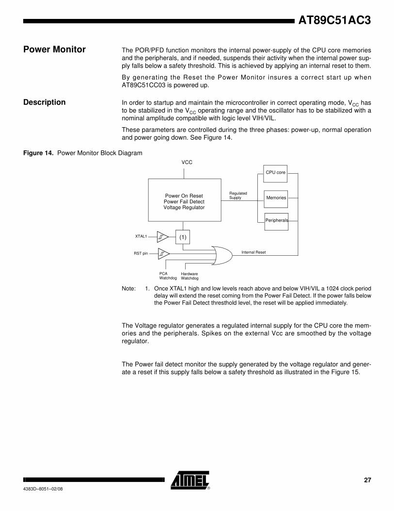
Power Monitor The POR/PFD function monitors the internal power-supply of the CPU core memories
and the peripherals, and if needed, suspends their activity when the internal power sup-
ply falls below a safety threshold. This is achieved by applying an internal reset to them.
By generating the Reset the Power Monitor insures a correct start up when
AT89C51CC03 is powered up.
Description In order to startup and maintain the microcontroller in correct operating mode, VCC has
to be stabilized in the VCC operating range and the oscillator has to be stabilized with a
nominal amplitude compatible with logic level VIH/VIL.
These parameters are controlled during the three phases: power-up, normal operation
and power going down. See Figure 14.
Figure 14. Power Monitor Block Diagram
Note: 1. Once XTAL1 high and low levels reach above and below VIH/VIL a 1024 clock period
delay will extend the reset coming from the Power Fail Detect. If the power falls below
the Power Fail Detect thresthold level, the reset will be applied immediately.
The Voltage regulator generates a regulated internal supply for the CPU core the mem-
ories and the peripherals. Spikes on the external Vcc are smoothed by the voltage
regulator.
The Power fail detect monitor the supply generated by the voltage regulator and gener-
ate a reset if this supply falls below a safety threshold as illustrated in the Figure 15.
VCC
Power On ResetPower Fail DetectVoltage Regulator
XTAL1 (1)
CPU core
Memories
Peripherals
RegulatedSupply
RST pin
HardwareWatchdog
PCAWatchdog
Internal Reset

28 AT89C51AC34383D–8051–02/08
Figure 15. Power Fail Detect
When the power is applied, the Power Monitor immediately asserts a reset. Once the
internal supply after the voltage regulator reach a safety level, the power monitor then
looks at the XTAL clock input. The internal reset will remain asserted until the Xtal1 lev-
els are above and below VIH and VIL. Further more. An internal counter will count 1024
clock periods before the reset is de-asserted.
If the internal power supply falls below a safety level, a reset is immediately asserted.
.
Vcc
t
Reset
Vcc
29
AT89C51AC3
4383D–8051–02/08
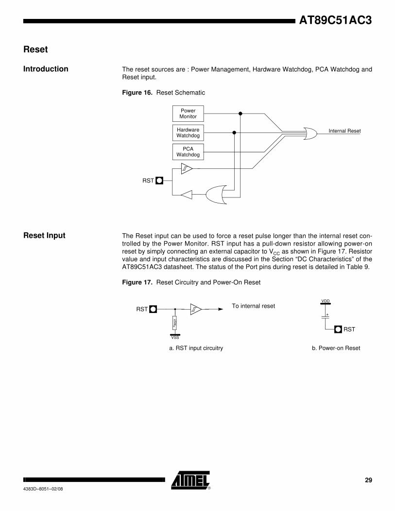
Reset
Introduction The reset sources are : Power Management, Hardware Watchdog, PCA Watchdog and
Reset input.
Figure 16. Reset Schematic
Reset Input The Reset input can be used to force a reset pulse longer than the internal reset con-
trolled by the Power Monitor. RST input has a pull-down resistor allowing power-on
reset by simply connecting an external capacitor to VCC as shown in Figure 17. Resistor
value and input characteristics are discussed in the Section “DC Characteristics” of the
AT89C51AC3 datasheet. The status of the Port pins during reset is detailed in Table 9.
Figure 17. Reset Circuitry and Power-On Reset
PowerMonitor
HardwareWatchdog
PCAWatchdog
RST
Internal Reset
RST
RR
ST
VSS
To internal reset
RST
VDD
+
b. Power-on Reseta. RST input circuitry

30 AT89C51AC34383D–8051–02/08
Reset Output
As detailed in Section “Watchdog Timer”, page 79, the WDT generates a 96-clock
period pulse on the RST pin. In order to properly propagate this pulse to the rest of the
application in case of external capacitor or power-supply supervisor circuit, a 1 kΩ resis-
tor must be added as shown Figure 18.
Figure 18. Recommended Reset Output Schematic
RST
VDD
+
VSS
VDD
RST
1K
To otheron-boardcircuitry
AT89C51AC3
31
AT89C51AC3
4383D–8051–02/08
Power Management
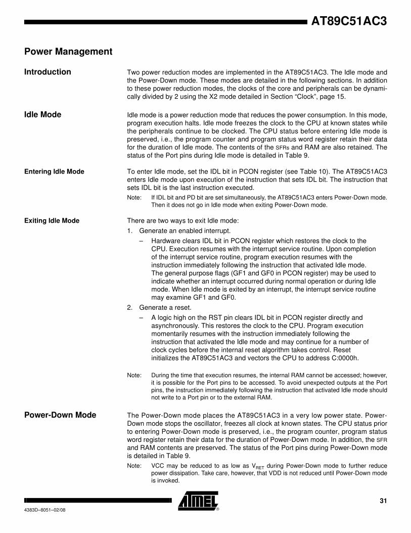
Introduction Two power reduction modes are implemented in the AT89C51AC3. The Idle mode and
the Power-Down mode. These modes are detailed in the following sections. In addition
to these power reduction modes, the clocks of the core and peripherals can be dynami-
cally divided by 2 using the X2 mode detailed in Section “Clock”, page 15.
Idle Mode Idle mode is a power reduction mode that reduces the power consumption. In this mode,
program execution halts. Idle mode freezes the clock to the CPU at known states while
the peripherals continue to be clocked. The CPU status before entering Idle mode is
preserved, i.e., the program counter and program status word register retain their data
for the duration of Idle mode. The contents of the SFRs and RAM are also retained. The
status of the Port pins during Idle mode is detailed in Table 9.
Entering Idle Mode To enter Idle mode, set the IDL bit in PCON register (see Table 10). The AT89C51AC3
enters Idle mode upon execution of the instruction that sets IDL bit. The instruction that
sets IDL bit is the last instruction executed.
Note: If IDL bit and PD bit are set simultaneously, the AT89C51AC3 enters Power-Down mode.
Then it does not go in Idle mode when exiting Power-Down mode.
Exiting Idle Mode There are two ways to exit Idle mode:
1. Generate an enabled interrupt.
– Hardware clears IDL bit in PCON register which restores the clock to the
CPU. Execution resumes with the interrupt service routine. Upon completion
of the interrupt service routine, program execution resumes with the
instruction immediately following the instruction that activated Idle mode.
The general purpose flags (GF1 and GF0 in PCON register) may be used to
indicate whether an interrupt occurred during normal operation or during Idle
mode. When Idle mode is exited by an interrupt, the interrupt service routine
may examine GF1 and GF0.
2. Generate a reset.
– A logic high on the RST pin clears IDL bit in PCON register directly and
asynchronously. This restores the clock to the CPU. Program execution
momentarily resumes with the instruction immediately following the
instruction that activated the Idle mode and may continue for a number of
clock cycles before the internal reset algorithm takes control. Reset
initializes the AT89C51AC3 and vectors the CPU to address C:0000h.
Note: During the time that execution resumes, the internal RAM cannot be accessed; however,
it is possible for the Port pins to be accessed. To avoid unexpected outputs at the Port
pins, the instruction immediately following the instruction that activated Idle mode should
not write to a Port pin or to the external RAM.
Power-Down Mode The Power-Down mode places the AT89C51AC3 in a very low power state. Power-
Down mode stops the oscillator, freezes all clock at known states. The CPU status prior
to entering Power-Down mode is preserved, i.e., the program counter, program status
word register retain their data for the duration of Power-Down mode. In addition, the SFR
and RAM contents are preserved. The status of the Port pins during Power-Down mode
is detailed in Table 9.
Note: VCC may be reduced to as low as VRET during Power-Down mode to further reduce
power dissipation. Take care, however, that VDD is not reduced until Power-Down mode
is invoked.
32 AT89C51AC34383D–8051–02/08
Entering Power-Down Mode To enter Power-Down mode, set PD bit in PCON register. The AT89C51AC3 enters the
Power-Down mode upon execution of the instruction that sets PD bit. The instruction
that sets PD bit is the last instruction executed.
Exiting Power-Down ModeNote: If VCC was reduced during the Power-Down mode, do not exit Power-Down mode until
VCC is restored to the normal operating level.
There are two ways to exit the Power-Down mode:
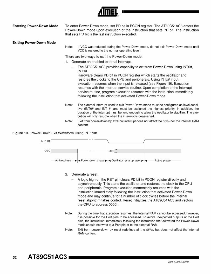
1. Generate an enabled external interrupt.
– The AT89C51AC3 provides capability to exit from Power-Down using INT0#,
INT1#.
Hardware clears PD bit in PCON register which starts the oscillator and
restores the clocks to the CPU and peripherals. Using INTx# input,
execution resumes when the input is released (see Figure 19). Execution
resumes with the interrupt service routine. Upon completion of the interrupt
service routine, program execution resumes with the instruction immediately
following the instruction that activated Power-Down mode.
Note: The external interrupt used to exit Power-Down mode must be configured as level sensi-
tive (INT0# and INT1#) and must be assigned the highest priority. In addition, the
duration of the interrupt must be long enough to allow the oscillator to stabilize. The exe-
cution will only resume when the interrupt is deasserted.
Note: Exit from power-down by external interrupt does not affect the SFRs nor the internal RAM
content.
Figure 19. Power-Down Exit Waveform Using INT1:0#
2. Generate a reset.
– A logic high on the RST pin clears PD bit in PCON register directly and
asynchronously. This starts the oscillator and restores the clock to the CPU
and peripherals. Program execution momentarily resumes with the
instruction immediately following the instruction that activated Power-Down
mode and may continue for a number of clock cycles before the internal
reset algorithm takes control. Reset initializes the AT89C51AC3 and vectors
the CPU to address 0000h.
Note: During the time that execution resumes, the internal RAM cannot be accessed; however,
it is possible for the Port pins to be accessed. To avoid unexpected outputs at the Port
pins, the instruction immediately following the instruction that activated the Power-Down
mode should not write to a Port pin or to the external RAM.
Note: Exit from power-down by reset redefines all the SFRs, but does not affect the internal
RAM content.
INT1:0#
OSC
Power-down phase Oscillator restart phase Active phaseActive phase
33
AT89C51AC3
4383D–8051–02/08
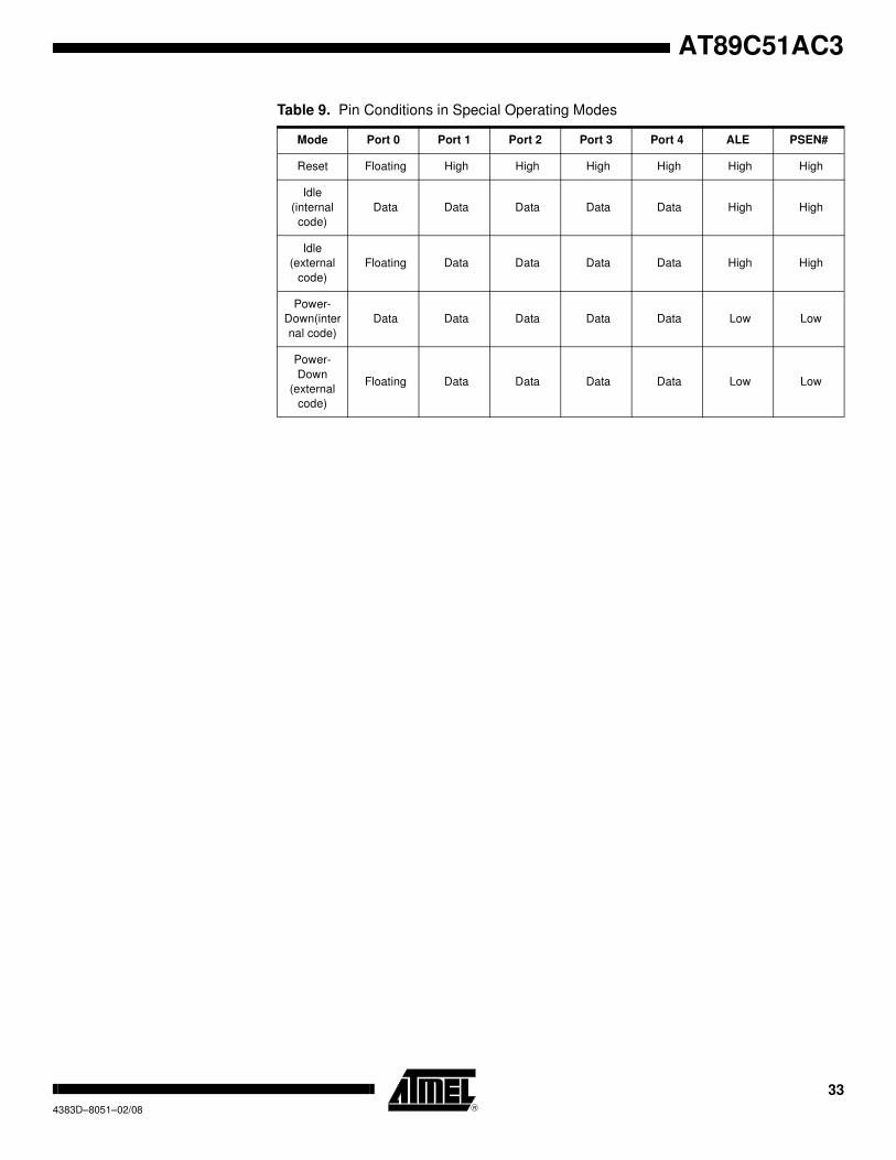
Table 9. Pin Conditions in Special Operating Modes
Mode Port 0 Port 1 Port 2 Port 3 Port 4 ALE PSEN#
Reset Floating High High High High High High
Idle
(internal
code)
Data Data Data Data Data High High
Idle
(external
code)
Floating Data Data Data Data High High
Power-
Down(inter
nal code)
Data Data Data Data Data Low Low
Power-
Down
(external
code)
Floating Data Data Data Data Low Low
34 AT89C51AC34383D–8051–02/08
Registers Table 10. PCON Register
PCON (S87:h) Power configuration Register
Reset Value= XXXX 0000b
7 6 5 4 3 2 1 0
- - - - GF1 GF0 PD IDL
Bit
Number
Bit
Mnemonic Description
7-4 -Reserved
The value read from these bits is indeterminate. Do not set these bits.
3 GF1
General Purpose flag 1
One use is to indicate whether an interrupt occurred during normal operation or
during Idle mode.
2 GF0
General Purpose flag 0
One use is to indicate whether an interrupt occurred during normal operation or
during Idle mode.
1 PD
Power-Down Mode bit
Cleared by hardware when an interrupt or reset occurs.
Set to activate the Power-Down mode.
If IDL and PD are both set, PD takes precedence.
0 IDL
Idle Mode bit
Cleared by hardware when an interrupt or reset occurs.
Set to activate the Idle mode.
If IDL and PD are both set, PD takes precedence.
35
AT89C51AC3
4383D–8051–02/08
EEPROM Data
Memory
The 2-Kbyte on-chip EEPROM memory block is located at addresses 0000h to 07FFh of
the XRAM/ERAM memory space and is selected by setting control bits in the EECON
register. A read in the EEPROM memory is done with a MOVX instruction.
A physical write in the EEPROM memory is done in two steps: write data in the column
latches and transfer of all data latches into an EEPROM memory row (programming).
The number of data written on the page may vary from 1 up to 128 Bytes (the page
size). When programming, only the data written in the column latch is programmed and
a ninth bit is used to obtain this feature. This provides the capability to program the
whole memory by Bytes, by page or by a number of Bytes in a page. Indeed, each ninth
bit is set when the writing the corresponding byte in a row and all these ninth bits are
reset after the writing of the complete EEPROM row.
Write Data in the Column Latches
Data is written by byte to the column latches as for an external RAM memory. Out of the
11 address bits of the data pointer, the 4 MSBs are used for page selection (row) and 7
are used for byte selection. Between two EEPROM programming sessions, all the
addresses in the column latches must stay on the same page, meaning that the 4 MSB
must no be changed.
The following procedure is used to write to the column latches:
• Save and disable interrupt.
• Set bit EEE of EECON register
• Load DPTR with the address to write
• Store A register with the data to be written
• Execute a MOVX @DPTR, A
• If needed loop the three last instructions until the end of a 128 Bytes page
• Restore interrupt.
Note: The last page address used when loading the column latch is the one used to select the
page programming address.
Programming The EEPROM programming consists of the following actions:
• writing one or more Bytes of one page in the column latches. Normally, all Bytes
must belong to the same page; if not, the first page address will be latched and the
others discarded.
• launching programming by writing the control sequence (50h followed by A0h) to the
EECON register.
• EEBUSY flag in EECON is then set by hardware to indicate that programming is in
progress and that the EEPROM segment is not available for reading.
• The end of programming is indicated by a hardware clear of the EEBUSY flag.
Note: The sequence 5xh and Axh must be executed without instructions between then other-
wise the programming is aborted.
Read Data The following procedure is used to read the data stored in the EEPROM memory:
• Save and disable interrupt
• Set bit EEE of EECON register
• Load DPTR with the address to read
• Execute a MOVX A, @DPTR
• Restore interrupt
36 AT89C51AC34383D–8051–02/08
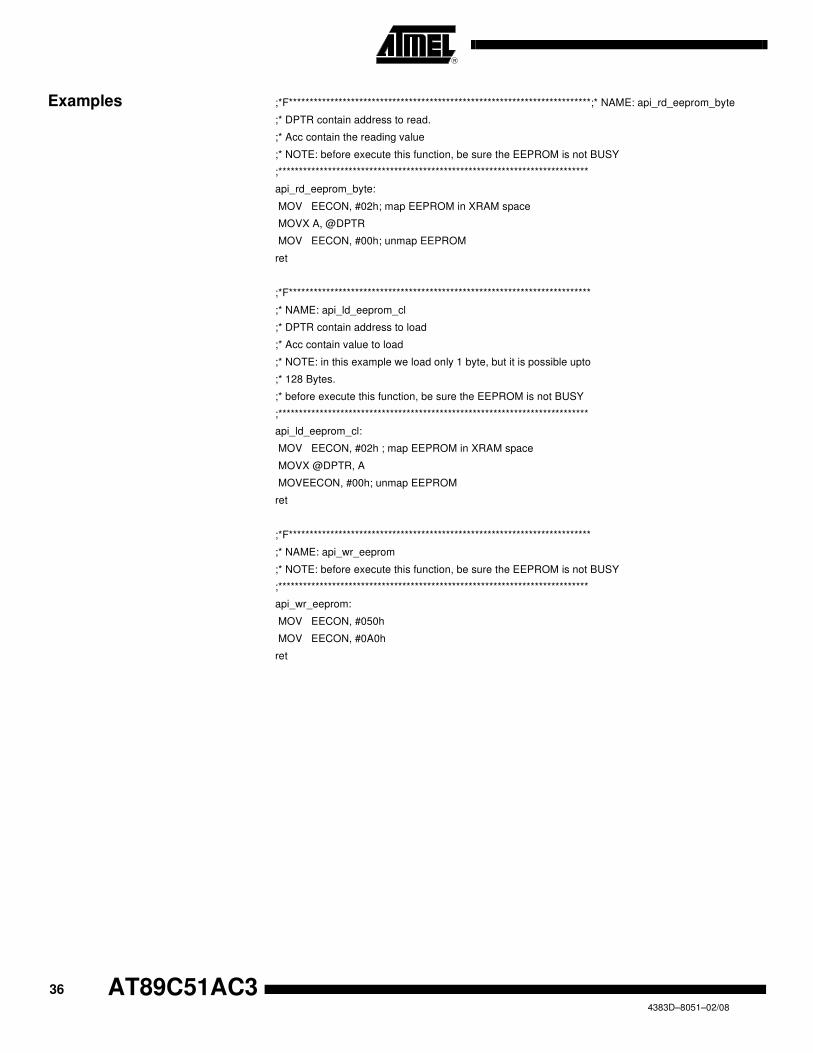
Examples ;*F*************************************************************************;* NAME: api_rd_eeprom_byte
;* DPTR contain address to read.
;* Acc contain the reading value
;* NOTE: before execute this function, be sure the EEPROM is not BUSY
;***************************************************************************
api_rd_eeprom_byte:
MOV EECON, #02h; map EEPROM in XRAM space
MOVX A, @DPTR
MOV EECON, #00h; unmap EEPROM
ret
;*F*************************************************************************
;* NAME: api_ld_eeprom_cl
;* DPTR contain address to load
;* Acc contain value to load
;* NOTE: in this example we load only 1 byte, but it is possible upto
;* 128 Bytes.
;* before execute this function, be sure the EEPROM is not BUSY
;***************************************************************************
api_ld_eeprom_cl:
MOV EECON, #02h ; map EEPROM in XRAM space
MOVX @DPTR, A
MOVEECON, #00h; unmap EEPROM
ret
;*F*************************************************************************
;* NAME: api_wr_eeprom
;* NOTE: before execute this function, be sure the EEPROM is not BUSY
;***************************************************************************
api_wr_eeprom:
MOV EECON, #050h
MOV EECON, #0A0h
ret

37
AT89C51AC3
4383D–8051–02/08
Registers Table 11. EECON Register
EECON (S:0D2h)
EEPROM Control Register
Reset Value = XXXX XX00b
Not bit addressable
7 6 5 4 3 2 1 0
EEPL3 EEPL2 EEPL1 EEPL0 - - EEE EEBUSY
Bit Number
Bit
Mnemonic Description
7-4 EEPL3-0Programming Launch command bits
Write 5Xh followed by AXh to EEPL to launch the programming.
3 -Reserved
The value read from this bit is indeterminate. Do not set this bit.
2 -Reserved
The value read from this bit is indeterminate. Do not set this bit.
1 EEE
Enable EEPROM Space bit
Set to map the EEPROM space during MOVX instructions (Write in the column
latches)
Clear to map the XRAM space during MOVX.
0 EEBUSY
Programming Busy flag
Set by hardware when programming is in progress.
Cleared by hardware when programming is done.
Can not be set or cleared by software.

38 AT89C51AC34383D–8051–02/08
Program/Code
Memory
The AT89C51AC3 implement 64K Bytes of on-chip program/code memory. Figure 20
shows the partitioning of internal and external program/code memory spaces depending
on the product.
The Flash memory increases EPROM and ROM functionality by in-circuit electrical era-
sure and programming. Thanks to the internal charge pump, the high voltage needed for
programming or erasing Flash cells is generated on-chip using the standard VDD volt-
age. Thus, the Flash Memory can be programmed using only one voltage and allows In-
System Programming commonly known as ISP. Hardware programming mode is also
available using specific programming tool.
Figure 20. Program/Code Memory Organization
0000h
64K Bytes
FFFFh
internal
0000h
FFFFh
Flash
64K Bytesexternalmemory
EA = 0EA = 1

39
AT89C51AC3
4383D–8051–02/08
External Code Memory Access
Memory Interface The external memory interface comprises the external bus (port 0 and port 2) as well as
the bus control signals (PSEN#, and ALE).
Figure 21 shows the structure of the external address bus. P0 carries address A7:0
while P2 carries address A15:8. Data D7:0 is multiplexed with A7:0 on P0. Table 21
describes the external memory interface signals.
Figure 21. External Code Memory Interface Structure
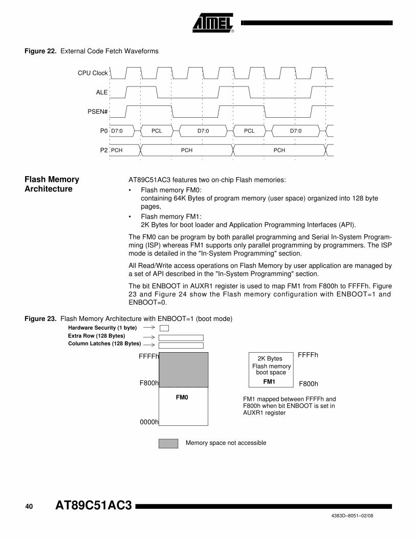
External Bus Cycles This section describes the bus cycles the AT89C51AC3 executes to fetch code (see
Figure 22) in the external program/code memory.
External memory cycle takes 6 CPU clock periods. This is equivalent to 12 oscillator
clock period in standard mode or 6 oscillator clock periods in X2 mode. For further infor-
mation on X2 mode see section “Clock “.
For simplicity, the accompanying figure depicts the bus cycle waveforms in idealized
form and do not provide precise timing information.
For bus cycling parameters refer to the ‘AC-DC parameters’ section.
Table 12. External Code Memory Interface Signals
Signal
Name Type Description
Alternate
Function
A15:8 OAddress Lines
Upper address lines for the external bus.P2.7:0
AD7:0 I/OAddress/Data Lines
Multiplexed lower address lines and data for the external memory.P0.7:0
ALE O
Address Latch Enable
ALE signals indicates that valid address information are available on lines
AD7:0.
-
PSEN# O
Program Store Enable Output
This signal is active low during external code fetch or external code read
(MOVC instruction).
-
Flash
EPROMAT89C51AC3
P2
P0AD7:0
A15:8
A7:0
A15:8
D7:0
A7:0
ALELatch
OEPSEN#
40 AT89C51AC34383D–8051–02/08
Figure 22. External Code Fetch Waveforms
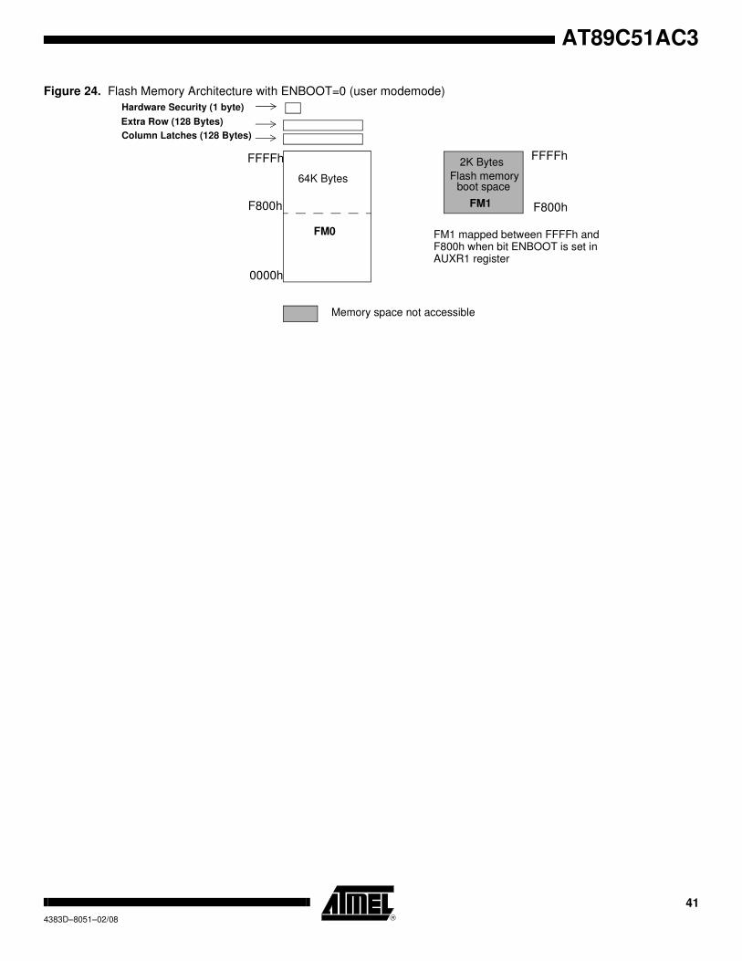
Flash Memory Architecture
AT89C51AC3 features two on-chip Flash memories:
• Flash memory FM0:
containing 64K Bytes of program memory (user space) organized into 128 byte
pages,
• Flash memory FM1:
2K Bytes for boot loader and Application Programming Interfaces (API).
The FM0 can be program by both parallel programming and Serial In-System Program-
ming (ISP) whereas FM1 supports only parallel programming by programmers. The ISP
mode is detailed in the "In-System Programming" section.
All Read/Write access operations on Flash Memory by user application are managed by
a set of API described in the "In-System Programming" section.
The bit ENBOOT in AUXR1 register is used to map FM1 from F800h to FFFFh. Figure
23 and Figure 24 show the Flash memory configuration with ENBOOT=1 and
ENBOOT=0.
Figure 23. Flash Memory Architecture with ENBOOT=1 (boot mode)
ALE
P0
P2
PSEN#
PCL
PCHPCH
PCLD7:0 D7:0
PCH
D7:0
CPU Clock
FFFFh
64K Bytes
FM0
0000h
Hardware Security (1 byte)
Column Latches (128 Bytes)
Extra Row (128 Bytes)
2K Bytes
Flash memory
FM1
boot space
FFFFh
F800h
FM1 mapped between FFFFh andF800h when bit ENBOOT is set in AUXR1 register
F800h
Memory space not accessible
41
AT89C51AC3
4383D–8051–02/08
Figure 24. Flash Memory Architecture with ENBOOT=0 (user modemode)
FFFFh
64K Bytes
FM0
0000h
Hardware Security (1 byte)
Column Latches (128 Bytes)
Extra Row (128 Bytes)
2K Bytes
Flash memory
FM1
boot space
FFFFh
F800h
FM1 mapped between FFFFh andF800h when bit ENBOOT is set in AUXR1 register
F800h
Memory space not accessible

42 AT89C51AC34383D–8051–02/08
FM0 Memory Architecture The Flash memory is made up of 4 blocks (see Figure 23):
• The memory array (user space) 64K Bytes
• The Extra Row
• The Hardware security bits
• The column latch registers
User Space This space is composed of a 64K Bytes Flash memory organized in 512 pages of 128
Bytes. It contains the user’s application code.
Extra Row (XRow) This row is a part of FM0 and has a size of 128 Bytes. The extra row may contain infor-
mation for boot loader usage.
Hardware security Byte (HSB) The Hardware security Byte space is a part of FM0 and has a size of 1 byte.
The 4 MSB can be read/written by software (from FM0 and , the 4 LSB can only be read
by software and written by hardware in parallel mode.
H Hardware Security Byte (HSB)
Column Latches The column latches, also part of FM0, have a size of full page (128 Bytes).
The column latches are the entrance buffers of the three previous memory locations
(user array, XROW and Hardware security byte). The column latches are write only and
can be accessed only from FM1 (boot mode) and from external memory
Cross Flash Memory Access
Description
The FM0 memory can be program only from FM1. Programming FM0 from FM0 or from
external memory is impossible.
The FM1 memory can be program only by parallel programming.
The Table show all software Flash access allowed.
7 6 5 4 3 2 1 0
X2 BLJB - - - LB2 LB1 LB0
Bit
Number
Bit
Mnemonic Description
7 X2
X2 Mode
Programmed (=’0’) to force X2 mode (6 clocks per instruction) after reset
Unprogrammed to force X1 mode, Standard Mode, afetr reset (Default)
6 BLJB
Boot Loader Jump Bit
When unprogrammed (=’1’), at the next reset :
-ENBOOT=0 (see code space memory configuration)
-Start address is 0000h (PC=0000h)
When programmed (=’0’)at the nex reset:
-ENBOOT=1 (see code space memory configuration)
-Start address is F800h (PC=F800h)
5 - Reserved
4 - Reserved
3 - Reserved
2-0 LB2-0General Memory Lock Bits (only programmable by programmer tools)
Section “Flash Protection from Parallel Programming”, page 51

43
AT89C51AC3
4383D–8051–02/08
Cross Flash Memory Access
(a) Depend upon general lock bit configuration.
Co
de
ex
ec
uti
ng
fro
m
Action
FM0
(user Flash)
FM1
(boot Flash)
FM0
(user Flash)
Read ok -
Load column latch ok -
Write - -
FM1
(boot Flash)
Read ok ok
Load column latch ok -
Write ok -
External
memory
EA = 0
Read (a) -
Load column latch - -
Write - -

44 AT89C51AC34383D–8051–02/08
Overview of FM0 Operations
Flash Registers (SFR)
The CPU interfaces to the flash memory through the FCON register, AUXR1 register
and FSTA register.
These registers are used to map the column latches, HSB, extra row and EEDATA in
the working data or code space.
FCON Register
Table 13. FCON Register
FCON Register (S:D1h)
Flash Control Register
Reset Value= 0000 0000b
7 6 5 4 3 2 1 0
FPL3 FPL2 FPL1 FPL0 FPS FMOD1 FMOD0 FBUSY
Bit
Number
Bit
Mnemonic Description
7-4 FPL3:0
Programming Launch Command Bits
Write 5Xh followed by AXh to launch the programming according to FMOD1:0.
(see Table 16.)
3 FPS
Flash Map Program Space
When this bit is set:
The MOVX @DPTR, A instruction writes in the columns latches space
When this bit is cleared:
The MOVX @DPTR, A instruction writes in the regular XDATA memory space
2-1 FMOD1:0Flash Mode
See Table 16.
0 FBUSY
Flash Busy
Set by hardware when programming is in progress.
Clear by hardware when programming is done.
Can not be changed by software.

45
AT89C51AC3
4383D–8051–02/08
FSTA Register
Table 14. FSTA Register
FSTA Register (S:D3h)
Flash Status Register
Reset Value= 0000 0000b
Mapping of the Memory Space By default, the user space is accessed by MOVC A, @DPTR instruction for read only.
The column latches space is made accessible by setting the FPS bit in FCON register.
Writing is possible from 0000h to FFFFh, address bits 6 to 0 are used to select an
address within a page while bits 15 to 7 are used to select the programming address of
the page.
Setting FPS bit takes precedence on the EXTRAM bit in AUXR register.
The other memory spaces (user, extra row, hardware security) are made accessible in
the code segment by programming bits FMOD0 and FMOD1 in FCON register in accor-
dance with Table 15. A MOVC instruction is then used for reading these spaces.
Table 15. FM0 Blocks Select Bits
Notes: 1. The column latches reset is a new option introduced in the AT89C51AC3, and is not
available in T89C51CC01/2
Launching Programming FPL3:0 bits in FCON register are used to secure the launch of programming. A specific
sequence must be written in these bits to unlock the write protection and to launch the
programming. This sequence is 5xh followed by Axh. Table 16 summarizes the memory
spaces to program according to FMOD1:0 bits.
7 6 5 4 3 2 1 0
SEQERR FLOAD
Bit
Number
Bit
Mnemonic Description
7-2 unusesd
1 SEQERR
Flash activation sequence error
Set by hardware when the flash activation sequence(MOV FCON 5X and MOV
FCON AX )is not correct (See Error Repport Section)
Clear by software or clear by hardware if the last activation sequence was
correct (previous error are canceled)
0 FLOAD
Flash Colums latch loaded
Set by hardware when the first data is loaded in the column latches.
Clear by hardware when the activation sequence suceed (flash write sucess, or
reset column latch success)
FMOD1 FMOD0 FM0 Adressable space
0 0 User (0000h-FFFFh)
0 1 Extra Row(FF80h-FFFFh)
1 0 Hardware Security Byte (0000h)
1 1 Column latches reset (note1)

46 AT89C51AC34383D–8051–02/08
Table 16. Programming Spaces
Notes: 1. The sequence 5xh and Axh must be executing without instructions between them
otherwise the programming is not executed (see Flash Status Register)
2. The sequence 5xh and Axh must be executed with the same FMOD0 FMOD1
configuration.
3. Interrupts that may occur during programming time must be disabled to avoid any
spurious exit of the programming mode.
Status of the Flash Memory The bit FBUSY in FCON register is used to indicate the status of programming.
FBUSY is set when programming is in progress.
The flash programming process is launched the second machine cycle following the
sequence 5xh and Axh in FCON. Thus the FBUSY flag should be read by sofware not
during the insctruction after the 5xh, Axh sequence but the the second instruction after
the 5xh, Axh sequence in FCON (See next example). FBUSY is cleared when the pro-
gramming is completed.
;*F*************************************************************************
;* NAME: launch_prog
;;***************************************************************************
launch_prog:
MOV FCON, #050h
MOV FCON #0A0h ; Flash Write Sequence
NOP ;Required time before reading busy flag
wait_busy:
MOV A,FCON
JB ACC.0,wait_busy
RET
Selecting FM1 The bit ENBOOT in AUXR1 register is used to map FM1 from F800h to FFFFh.
Loading the Column Latches Any number of data from 1-byte to 128 Bytes can be loaded in the column latches. This
provides the capability to program the whole memory by byte, by page or by any number
of Bytes in a page. Data written in the column latches do not have to be in consecutive
Write to FCON
OperationFPL3:0 FPS FMOD1 FMOD0
User
5 X 0 0 No action
A X 0 0Write the column latches in user
space
Extra Row
5 X 0 1 No action
A X 0 1Write the column latches in extra row
space
Hardware
Security
Byte
5 X 1 0 No action
A X 1 0 Write the fuse bits space
Reset
Columns
Latches
5 X 1 1 No action
A X 1 1 Reset the column latches

47
AT89C51AC3
4383D–8051–02/08
order. The page address of the last address loaded in the column latches will be used
for the whole page.
When programming is launched, an automatic erase of the locations loaded in the col-
umn latches is first performed, then programming is effectively done. Thus no page or
block erase is needed and only the loaded data are programmed in the corresponding
page
Notes: 1. : If no bytes are written in the column latches the SEQERR bit in the FSTA register
will be set.
2. When a flash write sequence is in progress (FBUSY is set) a write sequence to the
column latches will be ignored and the content of the column latches at the time of
the launch write sequence will be preserved.
3. MOVX @DPTR, A instruction must be used to load the column latches. Never use
MOVX @Ri, A instructions.
4. When a programming sequence is launched, Flash bytes corresponding to activated
bytes in the column latches are first erased then the bytes in the column latches are
copied into the Flash bytes. Flash bytes corresponding to bytes in the column latches
not activated (not loaded during the load column latches sequence) will not be erased
and written.
The following procedure is used to load the column latches and is summarized in
Figure 25:
• Save and Disable interrupt and map the column latch space by setting FPS bit.
• Load the DPTR with the address to load.
• Load Accumulator register with the data to load.
• Execute the MOVX @DPTR, A instruction.
• If needed loop the three last instructions until the page is completely loaded.
• unmap the column latch.
• Restore Interrupt

48 AT89C51AC34383D–8051–02/08
Figure 25. Column Latches Loading Procedure
Note: The last page address used when loading the column latch is the one used to select the
page programming address.
Programming the Flash Spaces
User The following procedure is used to program the User space and is summarized in
Figure 26:
• Load up to one page of data in the column latches from address 0000h to FFFFh.
• Save and Disable the interrupts.
• Launch the programming by writing the data sequence 50h followed by A0h in
FCON register (only from FM1).
The end of the programming indicated by the FBUSY flag cleared.
• Restore the interrupts.
Extra Row The following procedure is used to program the Extra Row space and is summarized in
Figure 26:
• Load data in the column latches from address FF80h to FFFFh.
• Save and Disable the interrupts.
• Launch the programming by writing the data sequence 52h followed by A2h in
FCON register (only from FM1).
The end of the programming indicated by the FBUSY flag cleared.
• Restore the interrupts.
Column Latches
Loading
Data LoadDPTR = Address
ACC = DataExec: MOVX @DPTR, A
Last Byte
to load?
Column Latches MappingFCON = 08h (FPS=1)
Data memory MappingFCON = 00h (FPS = 0)
Save and Disable ITEA = 0
Restore IT
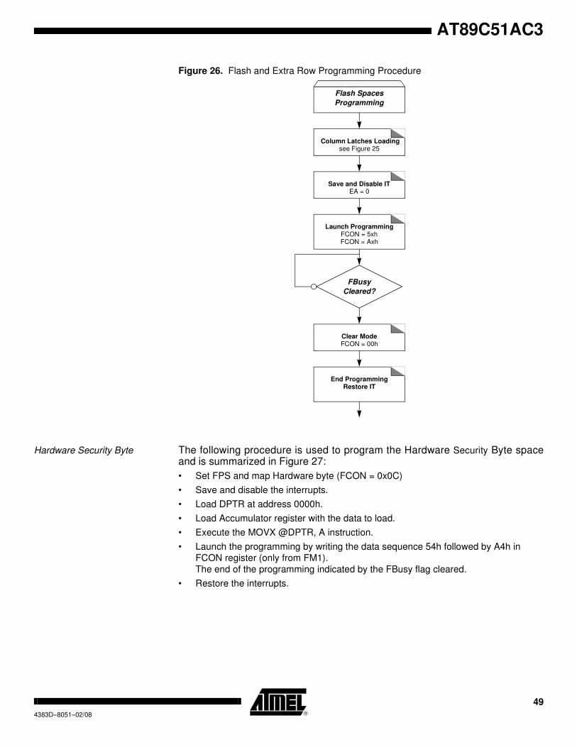
49
AT89C51AC3
4383D–8051–02/08
Figure 26. Flash and Extra Row Programming Procedure
Hardware Security Byte The following procedure is used to program the Hardware Security Byte spaceand is summarized in Figure 27:
• Set FPS and map Hardware byte (FCON = 0x0C)
• Save and disable the interrupts.
• Load DPTR at address 0000h.
• Load Accumulator register with the data to load.
• Execute the MOVX @DPTR, A instruction.
• Launch the programming by writing the data sequence 54h followed by A4h in
FCON register (only from FM1).
The end of the programming indicated by the FBusy flag cleared.
• Restore the interrupts.
Flash Spaces
Programming
Save and Disable ITEA = 0
Launch ProgrammingFCON = 5xhFCON = Axh
End ProgrammingRestore IT
Column Latches Loadingsee Figure 25
FBusy
Cleared?
Clear ModeFCON = 00h

50 AT89C51AC34383D–8051–02/08
Figure 27. Hardware Programming Procedure
Reset the Column Latches An automatic reset of the column latches is performed after a successful Flashwrite sequence. User can also reset the column latches manually, for instanceto reload the column latches before writing the Flash. The following procedure issummarized below.
• Save and disable the interrupts.
• Launch the reset by writing the data sequence 56h followed by A6h in FCON
register (only from FM1).
• Restore the interrupts.
Error Reports
Flash Programming Sequence
Errors
When a wrong sequence is detected, the SEQERR bit in FSTA register is set. Possible
wrong sequence are :
• MOV FCON, 5xh instruction not immediately followed by a MOV FCON, Ax
instruction.
• A write Flash sequence is launched while no data were loaded in the column latches
The SEQERR bit can be cleared
• By software
• By hardware when a correct programming sequence is completed
When multiple pages are written into the Flash, the user should check FSTA for errors
after each write page sequences, not only at the end of the multiple write pages.
Flash Spaces
Programming
Save and Disable ITEA = 0
Launch ProgrammingFCON = 54hFCON = A4h
End ProgrammingRestoreIT
FBusy
Cleared?
Clear ModeFCON = 00h
Data LoadDPTR = 00hACC = Data
Exec: MOVX @DPTR, A
FCON = 0Ch
Save and Disable ITEA = 0
End LoadingRestore IT

51
AT89C51AC3
4383D–8051–02/08
Power Down Request Before entering in Power Down (Set bit PD in PCON register) the user should check that
no write sequence is in progress (check BUSY=0), then check that the column latches
are reset (FLOAD=0 in FSTA register. Launch a reset column latches to clear FLOAD if
necessary.
Reading the Flash Spaces
User The following procedure is used to read the User space:
• Read one byte in Accumulator by executing MOVC A,@A+DPTR with
A+DPTR=read@.
Note: FCON is supposed to be reset when not needed.
Extra Row The following procedure is used to read the Extra Row space and is summarized in
Figure 28:
• Map the Extra Row space by writing 02h in FCON register.
• Read one byte in Accumulator by executing MOVC A,@A+DPTR with A = 0 and
DPTR = FF80h to FFFFh.
• Clear FCON to unmap the Extra Row.
Hardware Security Byte The following procedure is used to read the Hardware Security space and issummarized in Figure 28:
• Map the Hardware Security space by writing 04h in FCON register.
• Read the byte in Accumulator by executing MOVC A,@A+DPTR with A = 0 and
DPTR = 0000h.
Figure 28. Clear FCON to unmap the Hardware Security Byte.Reading Procedure
Flash Protection from Parallel
Programming
The three lock bits in Hardware Security Byte (see "In-System Programming" section)
are programmed according to Table 17 provide different level of protection for the on-
chip code and data located in FM0 and FM1.
The only way to write this bits are the parallel mode. They are set by default to level 4
Flash Spaces Reading
Flash Spaces MappingFCON= 00000xx0b
Data ReadDPTR= Address
ACC= 0Exec: MOVC A, @A+DPTR
Clear ModeFCON = 00h

52 AT89C51AC34383D–8051–02/08
Table 17. Program Lock Bit
Program Lock bits
U: unprogrammed
P: programmed
WARNING: Security level 2 and 3 should only be programmed after Flash and Core
verification.
Program Lock Bits
Protection Description
Security
levelLB0 LB1 LB2
1 U U U No program lock features enabled.
2 P U U
MOVC instruction executed from external program memory are
disabled from fetching code bytes from internal memory, EA is sampled
and latched on reset, and further parallel programming of the Flash is
disabled.
ISP and software programming with API are still allowed.
Writing EEprom Data from external parallel programmer is disabled but
still allowed from internal code execution.
3 U P U
Same as 2, also verify through parallel programming interface is
disabled.
Writing And Reading EEPROM Data from external parallel programmer
is disabled but still allowed from internal code execution..
4 U U P Same as 3, also external execution is disabled
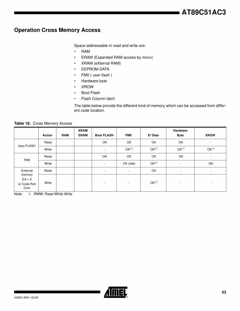
53
AT89C51AC3
4383D–8051–02/08
Operation Cross Memory Access
Space addressable in read and write are:
• RAM
• ERAM (Expanded RAM access by movx)
• XRAM (eXternal RAM)
• EEPROM DATA
• FM0 ( user flash )
• Hardware byte
• XROW
• Boot Flash
• Flash Column latch
The table below provide the different kind of memory which can be accessed from differ-
ent code location.
Note: 1. RWW: Read While Write
Table 18. Cross Memory Access
Action RAM
XRAM
ERAM Boot FLASH FM0 E² Data
Hardware
Byte XROW
boot FLASHRead OK OK OK OK -
Write - OK(1) OK(1) OK(1) OK(1)
FM0Read OK OK OK OK -
Write - OK (idle) OK(1) - OK
External
memory
EA = 0
or Code Roll
Over
Read - - OK - -
Write - - OK(1) - -

54 AT89C51AC34383D–8051–02/08
Sharing Instructions Table 19. Instructions shared
Note: by cl : using Column Latch
Table 20. Read MOVX A, @DPTR
Table 21. Write MOVX @DPTR,A
Action RAM
XRAM
ERAM
EEPROM
DATA
Boot
FLASH FM0
Hardware
Byte XROW
Read MOV MOVX MOVX MOVC MOVC MOVC MOVC
Write MOV MOVX MOVX - by cl by cl by cl
EEE bit in
EECON
Register
FPS in
FCON Register ENBOOT EA
XRAM
ERAM
EEPROM
DATA
Flash
Column
Latch
0 0 X X OK
0 1 X X OK
1 0 X X OK
1 1 X X OK
EEE bit in
EECON
Register
FPS bit in
FCON Register ENBOOT EA
XRAM
ERAM
EEPROM
Data
Flash
Column
Latch
0 0 X X OK
0 1 X1 OK
0 OK
1 0 X X OK
1 1 X1 OK
0 OK

55
AT89C51AC3
4383D–8051–02/08
Table 22. Read MOVC A, @DPTR
Code Execution
FCON Register
ENBOOT DPTR FM1 FM0 XROW
Hardware
Byte
External
CodeFMOD1 FMOD0 FPS
From FM0
0 0 X
0 0000h to FFFFh OK
10000h to F7FF OK
F800h to FFFFh Do not use this configuration
0 1 X X0000 to 007Fh
See (1)OK
1 0 X X X OK
1 1 X
0 000h to FFFFh OK
10000h to F7FF OK
F800h to FFFFh Do not use this configuration
From FM1
(ENBOOT =1
0 0
01
0000h to F7FF OK
F800h to FFFFh OK
0 X NA
11 X OK
0 X NA
0 1 X1 0000h to 007h
See (2)
OK
0 NA
1 0 X1
XOK
0 NA
1 1 X1
000h to FFFFhOK
0 NA
External code :
EA=0 or Code
Roll Over
X 0 X X X OK
1. For DPTR higher than 007Fh only lowest 7 bits are decoded, thus the behavior is the same as for addresses from 0000h to
007Fh
2. For DPTR higher than 007Fh only lowest 7 bits are decoded, thus the behavior is the same as for addresses from 0000h to
007Fh
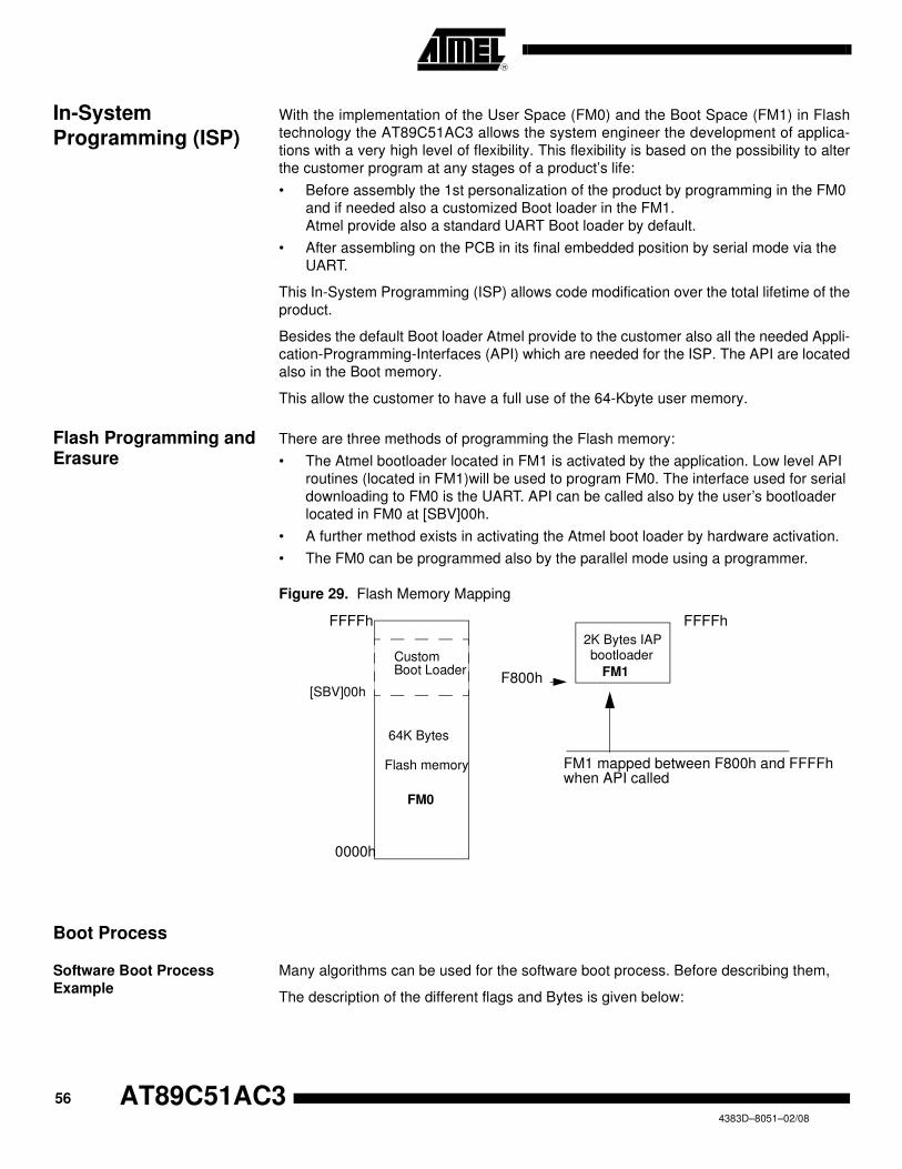
56 AT89C51AC34383D–8051–02/08
In-System
Programming (ISP)
With the implementation of the User Space (FM0) and the Boot Space (FM1) in Flash
technology the AT89C51AC3 allows the system engineer the development of applica-
tions with a very high level of flexibility. This flexibility is based on the possibility to alter
the customer program at any stages of a product’s life:
• Before assembly the 1st personalization of the product by programming in the FM0
and if needed also a customized Boot loader in the FM1.
Atmel provide also a standard UART Boot loader by default.
• After assembling on the PCB in its final embedded position by serial mode via the
UART.
This In-System Programming (ISP) allows code modification over the total lifetime of the
product.
Besides the default Boot loader Atmel provide to the customer also all the needed Appli-
cation-Programming-Interfaces (API) which are needed for the ISP. The API are located
also in the Boot memory.
This allow the customer to have a full use of the 64-Kbyte user memory.
Flash Programming and Erasure
There are three methods of programming the Flash memory:
• The Atmel bootloader located in FM1 is activated by the application. Low level API
routines (located in FM1)will be used to program FM0. The interface used for serial
downloading to FM0 is the UART. API can be called also by the user’s bootloader
located in FM0 at [SBV]00h.
• A further method exists in activating the Atmel boot loader by hardware activation.
• The FM0 can be programmed also by the parallel mode using a programmer.
Figure 29. Flash Memory Mapping
Boot Process
Software Boot Process
Example
Many algorithms can be used for the software boot process. Before describing them,
The description of the different flags and Bytes is given below:
F800h
FFFFh
64K Bytes
Flash memory
2K Bytes IAPbootloader
FM0
FM1CustomBoot Loader
[SBV]00h
FFFFh
FM1 mapped between F800h and FFFFhwhen API called
0000h

57
AT89C51AC3
4383D–8051–02/08
Boot Loader Jump Bit (BLJB):
- This bit indicates if on RESET the user wants to jump to this application at address
@0000h on FM0 or execute the boot loader at address @F800h on FM1.
- BLJB = 0 on parts delivered with bootloader programmed.
- To read or modify this bit, the APIs are used.
Boot Vector Address (SBV):
- This byte contains the MSB of the user boot loader address in FM0.
- The default value of SBV is FFh (no user boot loader in FM0).
- To read or modify this byte, the APIs are used.
Extra Byte (EB) and Boot Status Byte (BSB):
- These Bytes are reserved for customer use.
- To read or modify these Bytes, the APIs are used.
Hardware Boot Process At the falling edge of RESET, the bit ENBOOT in AUXR1 register is initialized with the
value of Boot Loader Jump Bit (BLJB).
Further at the falling edge of RESET if the following conditions (called Hardware condi-
tion) are detected:
• PSEN low,
• EA high,
• ALE high (or not connected).
– After Hardware Condition the FCON register is initialized with the value 00h
and the PC is initialized with F800h (FM1).
The Hardware condition makes the bootloader to be executed, whatever BLJB value is.
If no hardware condition is detected, the FCON register is initialized with the value F0h.
Check of the BLJB value.
• If bit BLJB = 1:
User application in FM0 will be started at @0000h (standard reset).
• If bit BLJB = 0:
Boot loader will be started at @F800h in FM1.
Note: 1. As PSEN is an output port in normal operating mode (running user applications or
bootloader applications) after reset it is recommended to release PSEN after the fall-
ing edge of Reset is signaled.
The hardware conditions are sampled at reset signal Falling Edge, thus they can be
released at any time when reset input is low.
2. To ensure correct microcontroller startup, the PSEN pin should not be tied to ground
during power-on.
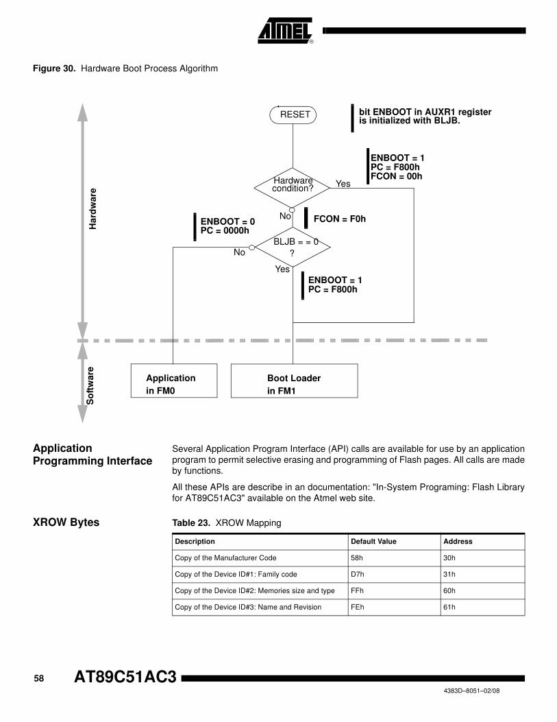
58 AT89C51AC34383D–8051–02/08
Figure 30. Hardware Boot Process Algorithm
Application Programming Interface
Several Application Program Interface (API) calls are available for use by an application
program to permit selective erasing and programming of Flash pages. All calls are made
by functions.
All these APIs are describe in an documentation: "In-System Programing: Flash Library
for AT89C51AC3" available on the Atmel web site.
XROW Bytes Table 23. XROW Mapping
RESET
Hardwarecondition?
BLJB = = 0
?
bit ENBOOT in AUXR1 registeris initialized with BLJB.
Hard
ware
So
ftw
are
ENBOOT = 1PC = F800h
ENBOOT = 1PC = F800h
FCON = 00h
FCON = F0h
Boot Loader
in FM1
ENBOOT = 0PC = 0000h
Yes
Yes
No
No
Application
in FM0
Description Default Value Address
Copy of the Manufacturer Code 58h 30h
Copy of the Device ID#1: Family code D7h 31h
Copy of the Device ID#2: Memories size and type FFh 60h
Copy of the Device ID#3: Name and Revision FEh 61h
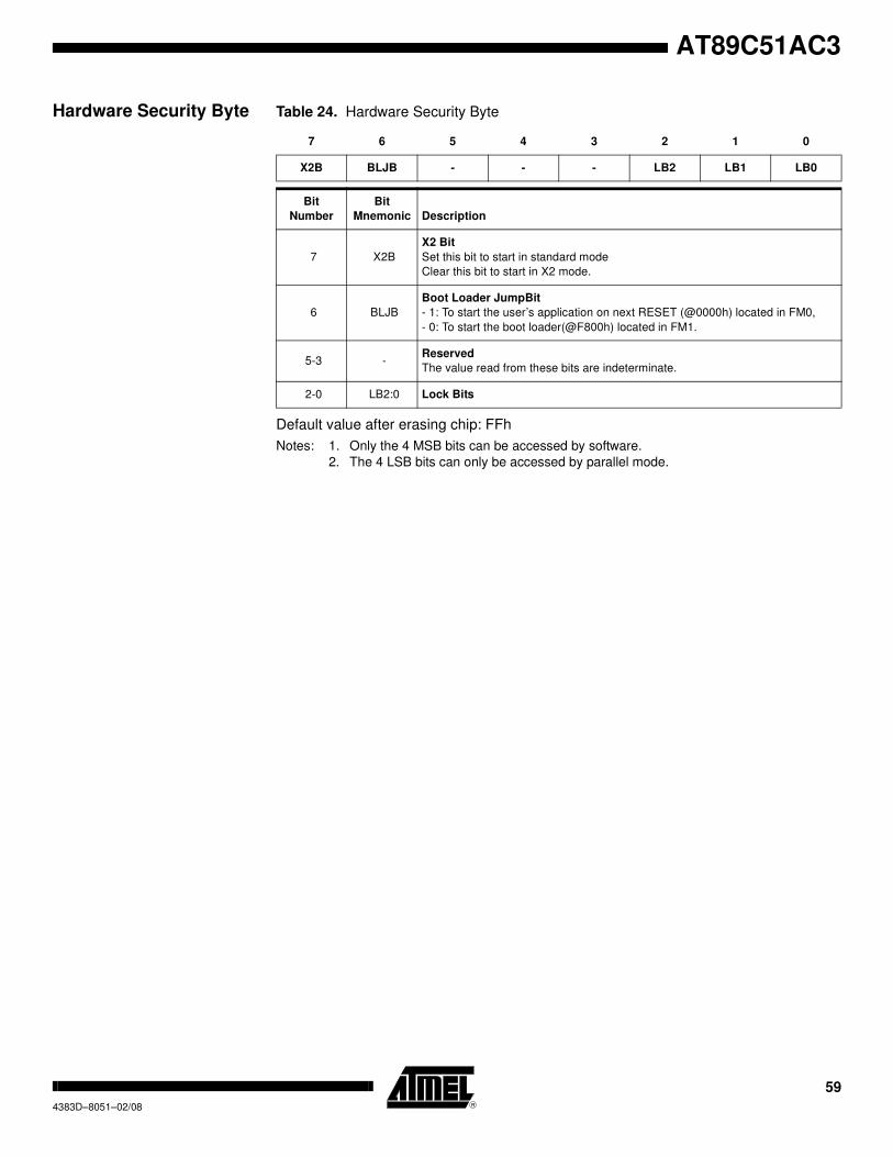
59
AT89C51AC3
4383D–8051–02/08
Hardware Security Byte Table 24. Hardware Security Byte
Default value after erasing chip: FFh
Notes: 1. Only the 4 MSB bits can be accessed by software.
2. The 4 LSB bits can only be accessed by parallel mode.
7 6 5 4 3 2 1 0
X2B BLJB - - - LB2 LB1 LB0
Bit
Number
Bit
Mnemonic Description
7 X2B
X2 Bit
Set this bit to start in standard mode
Clear this bit to start in X2 mode.
6 BLJB
Boot Loader JumpBit
- 1: To start the user’s application on next RESET (@0000h) located in FM0,
- 0: To start the boot loader(@F800h) located in FM1.
5-3 -Reserved
The value read from these bits are indeterminate.
2-0 LB2:0 Lock Bits
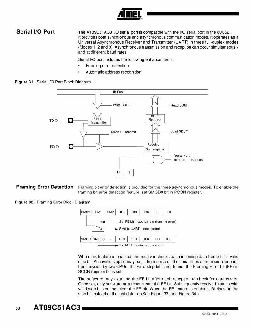
60 AT89C51AC34383D–8051–02/08
Serial I/O Port The AT89C51AC3 I/O serial port is compatible with the I/O serial port in the 80C52.
It provides both synchronous and asynchronous communication modes. It operates as a
Universal Asynchronous Receiver and Transmitter (UART) in three full-duplex modes
(Modes 1, 2 and 3). Asynchronous transmission and reception can occur simultaneously
and at different baud rates
Serial I/O port includes the following enhancements:
• Framing error detection
• Automatic address recognition
Figure 31. Serial I/O Port Block Diagram
Framing Error Detection Framing bit error detection is provided for the three asynchronous modes. To enable the
framing bit error detection feature, set SMOD0 bit in PCON register.
Figure 32. Framing Error Block Diagram
When this feature is enabled, the receiver checks each incoming data frame for a valid
stop bit. An invalid stop bit may result from noise on the serial lines or from simultaneous
transmission by two CPUs. If a valid stop bit is not found, the Framing Error bit (FE) in
SCON register bit is set.
The software may examine the FE bit after each reception to check for data errors.
Once set, only software or a reset clears the FE bit. Subsequently received frames with
valid stop bits cannot clear the FE bit. When the FE feature is enabled, RI rises on the
stop bit instead of the last data bit (See Figure 33. and Figure 34.).
Write SBUF
RI TI
SBUFTransmitter
SBUFReceiver
IB Bus
Mode 0 Transmit
Receive
Shift register
Load SBUF
Read SBUF
SCON reg
Interrupt Request
Serial Port
TXD
RXD
RITIRB8TB8RENSM2SM1SM0/FE
IDLPDGF0GF1POF-SMOD0SMOD
To UART framing error control
SM0 to UART mode control
Set FE bit if stop bit is 0 (framing error)

61
AT89C51AC3
4383D–8051–02/08
Figure 33. UART Timing in Mode 1
Figure 34. UART Timing in Modes 2 and 3
Automatic Address Recognition
The automatic address recognition feature is enabled when the multiprocessor commu-
nication feature is enabled (SM2 bit in SCON register is set).
Implemented in the hardware, automatic address recognition enhances the multiproces-
sor communication feature by allowing the serial port to examine the address of each
incoming command frame. Only when the serial port recognizes its own address will the
receiver set the RI bit in the SCON register to generate an interrupt. This ensures that
the CPU is not interrupted by command frames addressed to other devices.
If necessary, you can enable the automatic address recognition feature in mode 1. In
this configuration, the stop bit takes the place of the ninth data bit. Bit RI is set only when
the received command frame address matches the device’s address and is terminated
by a valid stop bit.
To support automatic address recognition, a device is identified by a given address and
a broadcast address.
Note: The multiprocessor communication and automatic address recognition features cannot
be enabled in mode 0 (i.e. setting SM2 bit in SCON register in mode 0 has no effect).
Data byte
RI
SMOD0=X
Stopbit
Startbit
RXD D7D6D5D4D3D2D1D0
FE
SMOD0=1
RI
SMOD0=0
Data byte Ninthbit
Stopbit
Startbit
RXD D8D7D6D5D4D3D2D1D0
RI
SMOD0=1
FE
SMOD0=1

62 AT89C51AC34383D–8051–02/08
Given Address Each device has an individual address that is specified in the SADDR register; the
SADEN register is a mask byte that contains don’t-care bits (defined by zeros) to form
the device’s given address. The don’t-care bits provide the flexibility to address one or
more slaves at a time. The following example illustrates how a given address is formed.
To address a device by its individual address, the SADEN mask byte must be 1111
1111b.
For example:SADDR0101 0110b
SADEN1111 1100b
Given0101 01XXb
Here is an example of how to use given addresses to address different slaves:Slave A:SADDR1111 0001b
SADEN1111 1010b
Given1111 0X0Xb
Slave B:SADDR1111 0011b
SADEN1111 1001b
Given1111 0XX1b
Slave C:SADDR1111 0011b
SADEN1111 1101b
Given1111 00X1b
The SADEN byte is selected so that each slave may be addressed separately.
For slave A, bit 0 (the LSB) is a don’t-care bit; for slaves B and C, bit 0 is a 1. To com-
municate with slave A only, the master must send an address where bit 0 is clear (e.g.
1111 0000b).
For slave A, bit 1 is a 0; for slaves B and C, bit 1 is a don’t care bit. To communicate with
slaves A and B, but not slave C, the master must send an address with bits 0 and 1 both
set (e.g. 1111 0011b).
To communicate with slaves A, B and C, the master must send an address with bit 0 set,
bit 1 clear, and bit 2 clear (e.g. 1111 0001b).
Broadcast Address A broadcast address is formed from the logical OR of the SADDR and SADEN registers
with zeros defined as don’t-care bits, e.g.:SADDR0101 0110b
SADEN1111 1100b
SADDR OR SADEN1111 111Xb
The use of don’t-care bits provides flexibility in defining the broadcast address, however
in most applications, a broadcast address is FFh. The following is an example of using
broadcast addresses:Slave A:SADDR1111 0001b
SADEN1111 1010b
Given1111 1X11b,
Slave B:SADDR1111 0011b
SADEN1111 1001b
Given1111 1X11B,
Slave C:SADDR=1111 0010b
SADEN1111 1101b
Given1111 1111b

63
AT89C51AC3
4383D–8051–02/08
For slaves A and B, bit 2 is a don’t care bit; for slave C, bit 2 is set. To communicate with
all of the slaves, the master must send an address FFh. To communicate with slaves A
and B, but not slave C, the master can send and address FBh.
Registers Table 25. SCON Register
SCON (S:98h)
Serial Control Register
Reset Value = 0000 0000b
Bit addressable
7 6 5 4 3 2 1 0
FE/SM0 SM1 SM2 REN TB8 RB8 TI RI
Bit
Number
Bit
Mnemonic Description
7 FE
Framing Error bit (SMOD0=1)
Clear to reset the error state, not cleared by a valid stop bit.
Set by hardware when an invalid stop bit is detected.
SM0Serial port Mode bit 0 (SMOD0=0)
Refer to SM1 for serial port mode selection.
6 SM1
Serial port Mode bit 1
SM0 SM1 Mode Baud Rate
0 0 Shift Register FXTAL/12 (or FXTAL /6 in mode X2)
0 1 8-bit UART Variable
1 0 9-bit UART FXTAL/64 or FXTAL/32
1 1 9-bit UART Variable
5 SM2
Serial port Mode 2 bit/Multiprocessor Communication Enable bit
Clear to disable multiprocessor communication feature.
Set to enable multiprocessor communication feature in mode 2 and 3.
4 REN
Reception Enable bit
Clear to disable serial reception.
Set to enable serial reception.
3 TB8
Transmitter Bit 8/Ninth bit to transmit in modes 2 and 3
Clear to transmit a logic 0 in the 9th bit.
Set to transmit a logic 1 in the 9th bit.
2 RB8
Receiver Bit 8/Ninth bit received in modes 2 and 3
Cleared by hardware if 9th bit received is a logic 0.
Set by hardware if 9th bit received is a logic 1.
1 TI
Transmit Interrupt flag
Clear to acknowledge interrupt.
Set by hardware at the end of the 8th bit time in mode 0 or at the beginning of the
stop bit in the other modes.
0 RI
Receive Interrupt flag
Clear to acknowledge interrupt.
Set by hardware at the end of the 8th bit time in mode 0, see Figure 33. and
Figure 34. in the other modes.

64 AT89C51AC34383D–8051–02/08
Table 26. SADEN Register
SADEN (S:B9h)
Slave Address Mask Register
Reset Value = 0000 0000b
Not bit addressable
Table 27. SADDR Register
SADDR (S:A9h)
Slave Address Register
Reset Value = 0000 0000b
Not bit addressable
Table 28. SBUF Register
SBUF (S:99h)
Serial Data Buffer
Reset Value = 0000 0000b
Not bit addressable
7 6 5 4 3 2 1 0
– – – – – – – –
Bit
Number
Bit
Mnemonic Description
7-0 Mask Data for Slave Individual Address
7 6 5 4 3 2 1 0
– – – – – – – –
Bit
Number
Bit
Mnemonic Description
7-0 Slave Individual Address
7 6 5 4 3 2 1 0
– – – – – – – –
Bit
Number
Bit
Mnemonic Description
7-0 Data sent/received by Serial I/O Port

65
AT89C51AC3
4383D–8051–02/08
Table 29. PCON Register
PCON (S:87h)
Power Control Register
Reset Value = 00X1 0000b
Not bit addressable
7 6 5 4 3 2 1 0
SMOD1 SMOD0 – POF GF1 GF0 PD IDL
Bit
Number
Bit
Mnemonic Description
7 SMOD1Serial port Mode bit 1
Set to select double baud rate in mode 1, 2 or 3.
6 SMOD0
Serial port Mode bit 0
Clear to select SM0 bit in SCON register.
Set to select FE bit in SCON register.
5 -Reserved
The value read from this bit is indeterminate. Do not set this bit.
4 POF
Power-Off Flag
Clear to recognize next reset type.
Set by hardware when VCC rises from 0 to its nominal voltage. Can also be set
by software.
3 GF1
General-purpose Flag
Cleared by user for general-purpose usage.
Set by user for general-purpose usage.
2 GF0
General-purpose Flag
Cleared by user for general-purpose usage.
Set by user for general-purpose usage.
1 PD
Power-Down mode bit
Cleared by hardware when reset occurs.
Set to enter power-down mode.
0 IDL
Idle mode bit
Clear by hardware when interrupt or reset occurs.
Set to enter idle mode.

66 AT89C51AC34383D–8051–02/08
Timers/Counters The AT89C51AC3 implements two general-purpose, 16-bit Timers/Counters. Such are
identified as Timer 0 and Timer 1, and can be independently configured to operate in a
variety of modes as a Timer or an event Counter. When operating as a Timer, the
Timer/Counter runs for a programmed length of time, then issues an interrupt request.
When operating as a Counter, the Timer/Counter counts negative transitions on an
external pin. After a preset number of counts, the Counter issues an interrupt request.
The various operating modes of each Timer/Counter are described in the following
sections.
Timer/Counter Operations
A basic operation is Timer registers THx and TLx (x = 0, 1) connected in cascade to
form a 16-bit Timer. Setting the run control bit (TRx) in TCON register (see Figure 30)
turns the Timer on by allowing the selected input to increment TLx. When TLx overflows
it increments THx; when THx overflows it sets the Timer overflow flag (TFx) in TCON
register. Setting the TRx does not clear the THx and TLx Timer registers. Timer regis-
ters can be accessed to obtain the current count or to enter preset values. They can be
read at any time but TRx bit must be cleared to preset their values, otherwise the behav-
ior of the Timer/Counter is unpredictable.
The C/Tx# control bit selects Timer operation or Counter operation by selecting the
divided-down peripheral clock or external pin Tx as the source for the counted signal.
TRx bit must be cleared when changing the mode of operation, otherwise the behavior
of the Timer/Counter is unpredictable.
For Timer operation (C/Tx# = 0), the Timer register counts the divided-down peripheral
clock. The Timer register is incremented once every peripheral cycle (6 peripheral clock
periods). The Timer clock rate is FPER/6, i.e. FOSC/12 in standard mode or FOSC/6 in X2
mode.
For Counter operation (C/Tx# = 1), the Timer register counts the negative transitions on
the Tx external input pin. The external input is sampled every peripheral cycles. When
the sample is high in one cycle and low in the next one, the Counter is incremented.
Since it takes 2 cycles (12 peripheral clock periods) to recognize a negative transition,
the maximum count rate is FPER/12, i.e. FOSC/24 in standard mode or FOSC/12 in X2
mode. There are no restrictions on the duty cycle of the external input signal, but to
ensure that a given level is sampled at least once before it changes, it should be held for
at least one full peripheral cycle.
Timer 0 Timer 0 functions as either a Timer or event Counter in four modes of operation.
Figure 35 to Figure 38 show the logical configuration of each mode.
Timer 0 is controlled by the four lower bits of TMOD register (see Figure 31) and bits 0,
1, 4 and 5 of TCON register (see Figure 30). TMOD register selects the method of Timer
gating (GATE0), Timer or Counter operation (T/C0#) and mode of operation (M10 and
M00). TCON register provides Timer 0 control functions: overflow flag (TF0), run control
bit (TR0), interrupt flag (IE0) and interrupt type control bit (IT0).
For normal Timer operation (GATE0 = 0), setting TR0 allows TL0 to be incremented by
the selected input. Setting GATE0 and TR0 allows external pin INT0# to control Timer
operation.
Timer 0 overflow (count rolls over from all 1s to all 0s) sets TF0 flag generating an inter-
rupt request.
It is important to stop Timer/Counter before changing mode.
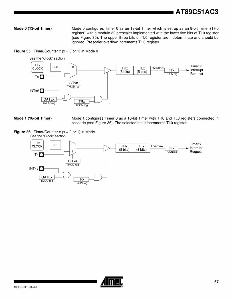
67
AT89C51AC3
4383D–8051–02/08
Mode 0 (13-bit Timer) Mode 0 configures Timer 0 as an 13-bit Timer which is set up as an 8-bit Timer (TH0
register) with a modulo 32 prescaler implemented with the lower five bits of TL0 register
(see Figure 35). The upper three bits of TL0 register are indeterminate and should be
ignored. Prescaler overflow increments TH0 register.
Figure 35. Timer/Counter x (x = 0 or 1) in Mode 0
Mode 1 (16-bit Timer) Mode 1 configures Timer 0 as a 16-bit Timer with TH0 and TL0 registers connected in
cascade (see Figure 36). The selected input increments TL0 register.
Figure 36. Timer/Counter x (x = 0 or 1) in Mode 1
FTxCLOCK
TRxTCON reg
TFxTCON reg
0
1
GATExTMOD reg
÷ 6 OverflowTimer xInterruptRequest
C/Tx#TMOD reg
TLx(5 bits)
THx(8 bits)
INTx#
Tx
See the “Clock” section
TRxTCON reg
TFxTCON reg
0
1
GATExTMOD reg
OverflowTimer xInterruptRequest
C/Tx#TMOD reg
TLx(8 bits)
THx(8 bits)
INTx#
Tx
FTxCLOCK ÷ 6
See the “Clock” section

68 AT89C51AC34383D–8051–02/08
Mode 2 (8-bit Timer with Auto-
Reload)
Mode 2 configures Timer 0 as an 8-bit Timer (TL0 register) that automatically reloads
from TH0 register (see Figure 37). TL0 overflow sets TF0 flag in TCON register and
reloads TL0 with the contents of TH0, which is preset by software. When the interrupt
request is serviced, hardware clears TF0. The reload leaves TH0 unchanged. The next
reload value may be changed at any time by writing it to TH0 register.
Figure 37. Timer/Counter x (x = 0 or 1) in Mode 2
Mode 3 (Two 8-bit Timers) Mode 3 configures Timer 0 such that registers TL0 and TH0 operate as separate 8-bit
Timers (see Figure 38). This mode is provided for applications requiring an additional 8-
bit Timer or Counter. TL0 uses the Timer 0 control bits C/T0# and GATE0 in TMOD reg-
ister, and TR0 and TF0 in TCON register in the normal manner. TH0 is locked into a
Timer function (counting FPER /6) and takes over use of the Timer 1 interrupt (TF1) and
run control (TR1) bits. Thus, operation of Timer 1 is restricted when Timer 0 is in mode
3.
Figure 38. Timer/Counter 0 in Mode 3: Two 8-bit Counters
TRxTCON reg
TFxTCON reg
0
1
GATExTMOD reg
OverflowTimer xInterruptRequest
C/Tx#TMOD reg
TLx(8 bits)
THx(8 bits)
INTx#
Tx
FTxCLOCK ÷ 6
See the “Clock” section
TR0TCON.4
TF0TCON.5
INT0#
0
1
GATE0TMOD.3
OverflowTimer 0InterruptRequest
C/T0#TMOD.2
TL0(8 bits)
TR1TCON.6
TH0(8 bits) TF1
TCON.7
OverflowTimer 1InterruptRequest
T0
FTxCLOCK ÷ 6
FTxCLOCK ÷ 6
See the “Clock” section
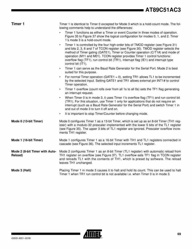
69
AT89C51AC3
4383D–8051–02/08
Timer 1 Timer 1 is identical to Timer 0 excepted for Mode 3 which is a hold-count mode. The fol-
lowing comments help to understand the differences:
• Timer 1 functions as either a Timer or event Counter in three modes of operation.
Figure 35 to Figure 37 show the logical configuration for modes 0, 1, and 2. Timer
1’s mode 3 is a hold-count mode.
• Timer 1 is controlled by the four high-order bits of TMOD register (see Figure 31)
and bits 2, 3, 6 and 7 of TCON register (see Figure 30). TMOD register selects the
method of Timer gating (GATE1), Timer or Counter operation (C/T1#) and mode of
operation (M11 and M01). TCON register provides Timer 1 control functions:
overflow flag (TF1), run control bit (TR1), interrupt flag (IE1) and interrupt type
control bit (IT1).
• Timer 1 can serve as the Baud Rate Generator for the Serial Port. Mode 2 is best
suited for this purpose.
• For normal Timer operation (GATE1 = 0), setting TR1 allows TL1 to be incremented
by the selected input. Setting GATE1 and TR1 allows external pin INT1# to control
Timer operation.
• Timer 1 overflow (count rolls over from all 1s to all 0s) sets the TF1 flag generating
an interrupt request.
• When Timer 0 is in mode 3, it uses Timer 1’s overflow flag (TF1) and run control bit
(TR1). For this situation, use Timer 1 only for applications that do not require an
interrupt (such as a Baud Rate Generator for the Serial Port) and switch Timer 1 in
and out of mode 3 to turn it off and on.
• It is important to stop Timer/Counter before changing mode.
Mode 0 (13-bit Timer) Mode 0 configures Timer 1 as a 13-bit Timer, which is set up as an 8-bit Timer (TH1 reg-
ister) with a modulo-32 prescaler implemented with the lower 5 bits of the TL1 register
(see Figure 35). The upper 3 bits of TL1 register are ignored. Prescaler overflow incre-
ments TH1 register.
Mode 1 (16-bit Timer) Mode 1 configures Timer 1 as a 16-bit Timer with TH1 and TL1 registers connected in
cascade (see Figure 36). The selected input increments TL1 register.
Mode 2 (8-bit Timer with Auto-
Reload)
Mode 2 configures Timer 1 as an 8-bit Timer (TL1 register) with automatic reload from
TH1 register on overflow (see Figure 37). TL1 overflow sets TF1 flag in TCON register
and reloads TL1 with the contents of TH1, which is preset by software. The reload
leaves TH1 unchanged.
Mode 3 (Halt) Placing Timer 1 in mode 3 causes it to halt and hold its count. This can be used to halt
Timer 1 when TR1 run control bit is not available i.e. when Timer 0 is in mode 3.

70 AT89C51AC34383D–8051–02/08
Interrupt Each Timer handles one interrupt source that is the timer overflow flag TF0 or TF1. This
flag is set every time an overflow occurs. Flags are cleared when vectoring to the Timer
interrupt routine. Interrupts are enabled by setting ETx bit in IEN0 register. This assumes
interrupts are globally enabled by setting EA bit in IEN0 register.
Figure 39. Timer Interrupt System
Registers Table 30. TCON Register
TCON (S:88h)
Timer/Counter Control Register
Reset Value = 0000 0000b
TF0TCON.5
ET0IEN0.1
Timer 0Interrupt Request
TF1TCON.7
ET1IEN0.3
Timer 1Interrupt Request
7 6 5 4 3 2 1 0
TF1 TR1 TF0 TR0 IE1 IT1 IE0 IT0
Bit
Number
Bit
Mnemonic Description
7 TF1
Timer 1 Overflow Flag
Cleared by hardware when processor vectors to interrupt routine.
Set by hardware on Timer/Counter overflow, when Timer 1 register overflows.
6 TR1
Timer 1 Run Control Bit
Clear to turn off Timer/Counter 1.
Set to turn on Timer/Counter 1.
5 TF0
Timer 0 Overflow Flag
Cleared by hardware when processor vectors to interrupt routine.
Set by hardware on Timer/Counter overflow, when Timer 0 register overflows.
4 TR0
Timer 0 Run Control Bit
Clear to turn off Timer/Counter 0.
Set to turn on Timer/Counter 0.
3 IE1
Interrupt 1 Edge Flag
Cleared by hardware when interrupt is processed if edge-triggered (see IT1).
Set by hardware when external interrupt is detected on INT1# pin.
2 IT1
Interrupt 1 Type Control Bit
Clear to select low level active (level triggered) for external interrupt 1 (INT1#).
Set to select falling edge active (edge triggered) for external interrupt 1.
1 IE0
Interrupt 0 Edge Flag
Cleared by hardware when interrupt is processed if edge-triggered (see IT0).
Set by hardware when external interrupt is detected on INT0# pin.
0 IT0
Interrupt 0 Type Control Bit
Clear to select low level active (level triggered) for external interrupt 0 (INT0#).
Set to select falling edge active (edge triggered) for external interrupt 0.

71
AT89C51AC3
4383D–8051–02/08
Table 31. TMOD Register
TMOD (S:89h)
Timer/Counter Mode Control Register
Reset Value = 0000 0000b
7 6 5 4 3 2 1 0
GATE1 C/T1# M11 M01 GATE0 C/T0# M10 M00
Bit
Number
Bit
Mnemonic Description
7 GATE1
Timer 1 Gating Control Bit
Clear to enable Timer 1 whenever TR1 bit is set.
Set to enable Timer 1 only while INT1# pin is high and TR1 bit is set.
6 C/T1#
Timer 1 Counter/Timer Select Bit
Clear for Timer operation: Timer 1 counts the divided-down system clock.
Set for Counter operation: Timer 1 counts negative transitions on external pin T1.
5 M11 Timer 1 Mode Select Bits
M11 M01 Operating mode
0 0 Mode 0: 8-bit Timer/Counter (TH1) with 5-bit prescaler (TL1).
0 1 Mode 1: 16-bit Timer/Counter.
1 0 Mode 2: 8-bit auto-reload Timer/Counter (TL1) (1)
1 1 Mode 3: Timer 1 halted. Retains count
1. Reloaded from TH1 at overflow.
4 M01
3 GATE0
Timer 0 Gating Control Bit
Clear to enable Timer 0 whenever TR0 bit is set.
Set to enable Timer/Counter 0 only while INT0# pin is high and TR0 bit is set.
2 C/T0#
Timer 0 Counter/Timer Select Bit
Clear for Timer operation: Timer 0 counts the divided-down system clock.
Set for Counter operation: Timer 0 counts negative transitions on external pin T0.
1 M10
Timer 0 Mode Select Bit
M10 M00 Operating mode
0 0 Mode 0: 8-bit Timer/Counter (TH0) with 5-bit prescaler (TL0).
0 1 Mode 1: 16-bit Timer/Counter.
1 0 Mode 2: 8-bit auto-reload Timer/Counter (TL0) (2)
1 1 Mode 3: TL0 is an 8-bit Timer/Counter
TH0 is an 8-bit Timer using Timer 1’s TR0 and TF0 bits.
2. Reloaded from TH0 at overflow.
0 M00

72 AT89C51AC34383D–8051–02/08
Table 32. TH0 Register
TH0 (S:8Ch)
Timer 0 High Byte Register
Reset Value = 0000 0000b
Table 33. TL0 Register
TL0 (S:8Ah)
Timer 0 Low Byte Register
Reset Value = 0000 0000b
Table 34. TH1 Register
TH1 (S:8Dh)
Timer 1 High Byte Register
Reset Value = 0000 0000b
7 6 5 4 3 2 1 0
– – – – – – – –
Bit
Number
Bit
Mnemonic Description
7:0 High Byte of Timer 0.
7 6 5 4 3 2 1 0
– – – – – – – –
Bit
Number
Bit
Mnemonic Description
7:0 Low Byte of Timer 0.
7 6 5 4 3 2 1 0
– – – – – – – –
Bit
Number
Bit
Mnemonic Description
7:0 High Byte of Timer 1.
73
AT89C51AC3
4383D–8051–02/08
Table 35. TL1 Register
TL1 (S:8Bh)
Timer 1 Low Byte Register
Reset Value = 0000 0000b
7 6 5 4 3 2 1 0
– – – – – – – –
Bit
Number
Bit
Mnemonic Description
7:0 Low Byte of Timer 1.

74 AT89C51AC34383D–8051–02/08
Timer 2 The AT89C51AC3 timer 2 is compatible with timer 2 in the 80C52.
It is a 16-bit timer/counter: the count is maintained by two eight-bit timer registers, TH2
and TL2 that are cascade- connected. It is controlled by T2CON register (See Table )
and T2MOD register (See Table 38). Timer 2 operation is similar to Timer 0 and Timer
1. C/T2 selects FT2 clock/6 (timer operation) or external pin T2 (counter operation) as
timer clock. Setting TR2 allows TL2 to be incremented by the selected input.
Timer 2 includes the following enhancements:
• Auto-reload mode (up or down counter)
• Programmable clock-output
Auto-Reload Mode The auto-reload mode configures timer 2 as a 16-bit timer or event counter with auto-
matic reload. This feature is controlled by the DCEN bit in T2MOD register (See
Table 38). Setting the DCEN bit enables timer 2 to count up or down as shown in
Figure 40. In this mode the T2EX pin controls the counting direction.
When T2EX is high, timer 2 counts up. Timer overflow occurs at FFFFh which sets the
TF2 flag and generates an interrupt request. The overflow also causes the 16-bit value
in RCAP2H and RCAP2L registers to be loaded into the timer registers TH2 and TL2.
When T2EX is low, timer 2 counts down. Timer underflow occurs when the count in the
timer registers TH2 and TL2 equals the value stored in RCAP2H and RCAP2L registers.
The underflow sets TF2 flag and reloads FFFFh into the timer registers.
The EXF2 bit toggles when timer 2 overflow or underflow, depending on the direction of
the count. EXF2 does not generate an interrupt. This bit can be used to provide 17-bit
resolution.
Figure 40. Auto-Reload Mode Up/Down Counter
(DOWN COUNTING RELOAD VALUE)
TF2
T2
EXF2
TH2(8-bit)
TL2(8-bit)
RCAP2H(8-bit)
RCAP2L(8-bit)
FFh(8-bit)
FFh(8-bit)
TOGGLE
(UP COUNTING RELOAD VALUE)
TIMER 2INTERRUPT
:6
T2CONreg
T2CONreg
T2EX:
1=UP
2=DOWN
0
1
CT/2T2CON.1
TR2T2CON.2
FT2CLOCK
see section “Clock”

75
AT89C51AC3
4383D–8051–02/08
Programmable Clock-Output
In clock-out mode, timer 2 operates as a 50%-duty-cycle, programmable clock genera-
tor (See Figure 41). The input clock increments TL2 at frequency FOSC/2. The timer
repeatedly counts to overflow from a loaded value. At overflow, the contents of RCAP2H
and RCAP2L registers are loaded into TH2 and TL2. In this mode, timer 2 overflows do
not generate interrupts. The formula gives the clock-out frequency depending on the
system oscillator frequency and the value in the RCAP2H and RCAP2L registers:
For a 16 MHz system clock in x1 mode, timer 2 has a programmable frequency range of
61 Hz (FOSC/216) to 4 MHz (FOSC/4). The generated clock signal is brought out to T2 pin
(P1.0).
Timer 2 is programmed for the clock-out mode as follows:
• Set T2OE bit in T2MOD register.
• Clear C/T2 bit in T2CON register.
• Determine the 16-bit reload value from the formula and enter it in RCAP2H/RCAP2L
registers.
• Enter a 16-bit initial value in timer registers TH2/TL2. It can be the same as the
reload value or different depending on the application.
• To start the timer, set TR2 run control bit in T2CON register.
It is possible to use timer 2 as a baud rate generator and a clock generator simulta-
neously. For this configuration, the baud rates and clock frequencies are not
independent since both functions use the values in the RCAP2H and RCAP2L registers.
Figure 41. Clock-Out Mode
Clock OutFrequency–FT2clock
4 65536 RCAP2H– RCAP2L⁄( )×-----------------------------------------------------------------------------------------=
EXEN2
EXF2
OVERFLOW
T2EX
TH2(8-bit)
TL2(8-bit)
TIMER 2
RCAP2H(8-bit)
RCAP2L(8-bit)
T2OE
T2CON reg
T2CON reg
T2MOD reg
INTERRUPT
TR2T2CON.2
FT2CLOCK
T2
Q D
Toggle
Q
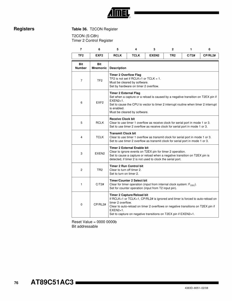
76 AT89C51AC34383D–8051–02/08
Registers Table 36. T2CON Register
T2CON (S:C8h)
Timer 2 Control Register
Reset Value = 0000 0000b
Bit addressable
7 6 5 4 3 2 1 0
TF2 EXF2 RCLK TCLK EXEN2 TR2 C/T2# CP/RL2#
Bit
Number
Bit
Mnemonic Description
7 TF2
Timer 2 Overflow Flag
TF2 is not set if RCLK=1 or TCLK = 1.
Must be cleared by software.
Set by hardware on timer 2 overflow.
6 EXF2
Timer 2 External Flag
Set when a capture or a reload is caused by a negative transition on T2EX pin if
EXEN2=1.
Set to cause the CPU to vector to timer 2 interrupt routine when timer 2 interrupt
is enabled.
Must be cleared by software.
5 RCLK
Receive Clock bit
Clear to use timer 1 overflow as receive clock for serial port in mode 1 or 3.
Set to use timer 2 overflow as receive clock for serial port in mode 1 or 3.
4 TCLK
Transmit Clock bit
Clear to use timer 1 overflow as transmit clock for serial port in mode 1 or 3.
Set to use timer 2 overflow as transmit clock for serial port in mode 1 or 3.
3 EXEN2
Timer 2 External Enable bit
Clear to ignore events on T2EX pin for timer 2 operation.
Set to cause a capture or reload when a negative transition on T2EX pin is
detected, if timer 2 is not used to clock the serial port.
2 TR2
Timer 2 Run Control bit
Clear to turn off timer 2.
Set to turn on timer 2.
1 C/T2#
Timer/Counter 2 Select bit
Clear for timer operation (input from internal clock system: FOSC).
Set for counter operation (input from T2 input pin).
0 CP/RL2#
Timer 2 Capture/Reload bit
If RCLK=1 or TCLK=1, CP/RL2# is ignored and timer is forced to auto-reload on
timer 2 overflow.
Clear to auto-reload on timer 2 overflows or negative transitions on T2EX pin if
EXEN2=1.
Set to capture on negative transitions on T2EX pin if EXEN2=1.

77
AT89C51AC3
4383D–8051–02/08
Table 37. T2MOD Register
T2MOD (S:C9h)
Timer 2 Mode Control Register
Reset Value = XXXX XX00b
Not bit addressable
Table 38. TH2 Register
TH2 (S:CDh)
Timer 2 High Byte Register
Reset Value = 0000 0000b
Not bit addressable
7 6 5 4 3 2 1 0
- - - - - - T2OE DCEN
Bit
Number
Bit
Mnemonic Description
7 -Reserved
The value read from this bit is indeterminate. Do not set this bit.
6 -Reserved
The value read from this bit is indeterminate. Do not set this bit.
5 -Reserved
The value read from this bit is indeterminate. Do not set this bit.
4 -Reserved
The value read from this bit is indeterminate. Do not set this bit.
3 -Reserved
The value read from this bit is indeterminate. Do not set this bit.
2 -Reserved
The value read from this bit is indeterminate. Do not set this bit.
1 T2OE
Timer 2 Output Enable bit
Clear to program P1.0/T2 as clock input or I/O port.
Set to program P1.0/T2 as clock output.
0 DCEN
Down Counter Enable bit
Clear to disable timer 2 as up/down counter.
Set to enable timer 2 as up/down counter.
7 6 5 4 3 2 1 0
- - - - - - - -
Bit
Number
Bit
Mnemonic Description
7-0 High Byte of Timer 2.

78 AT89C51AC34383D–8051–02/08
Table 39. TL2 Register
TL2 (S:CCh)
Timer 2 Low Byte Register
Reset Value = 0000 0000b
Not bit addressable
Table 40. RCAP2H Register
RCAP2H (S:CBh)
Timer 2 Reload/Capture High Byte Register
Reset Value = 0000 0000b
Not bit addressable
Table 41. RCAP2L Register
RCAP2L (S:CAH)
TIMER 2 REload/Capture Low Byte Register
Reset Value = 0000 0000b
Not bit addressable
7 6 5 4 3 2 1 0
- - - - - - - -
Bit
Number
Bit
Mnemonic Description
7-0 Low Byte of Timer 2.
7 6 5 4 3 2 1 0
- - - - - - - -
Bit
Number
Bit
Mnemonic Description
7-0 High Byte of Timer 2 Reload/Capture.
7 6 5 4 3 2 1 0
- - - - - - - -
Bit
Number
Bit
Mnemonic Description
7-0 Low Byte of Timer 2 Reload/Capture.
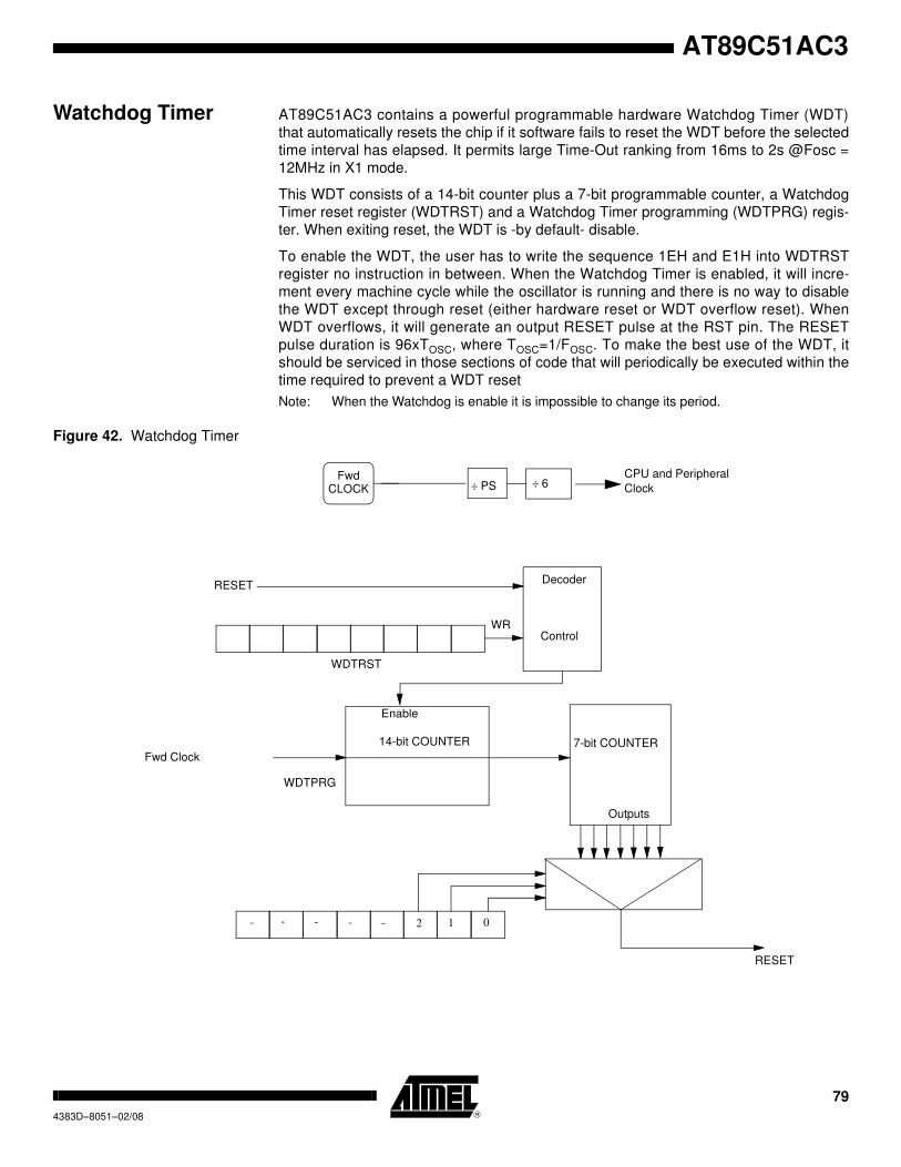
79
AT89C51AC3
4383D–8051–02/08
Watchdog Timer AT89C51AC3 contains a powerful programmable hardware Watchdog Timer (WDT)
that automatically resets the chip if it software fails to reset the WDT before the selected
time interval has elapsed. It permits large Time-Out ranking from 16ms to 2s @Fosc =
12MHz in X1 mode.
This WDT consists of a 14-bit counter plus a 7-bit programmable counter, a Watchdog
Timer reset register (WDTRST) and a Watchdog Timer programming (WDTPRG) regis-
ter. When exiting reset, the WDT is -by default- disable.
To enable the WDT, the user has to write the sequence 1EH and E1H into WDTRST
register no instruction in between. When the Watchdog Timer is enabled, it will incre-
ment every machine cycle while the oscillator is running and there is no way to disable
the WDT except through reset (either hardware reset or WDT overflow reset). When
WDT overflows, it will generate an output RESET pulse at the RST pin. The RESET
pulse duration is 96xTOSC, where TOSC=1/FOSC. To make the best use of the WDT, it
should be serviced in those sections of code that will periodically be executed within the
time required to prevent a WDT reset
Note: When the Watchdog is enable it is impossible to change its period.
Figure 42. Watchdog Timer
÷ 6÷ PSCPU and Peripheral
ClockFwd
CLOCK
WDTPRG
RESETDecoder
Control
WDTRST
WR
Enable
14-bit COUNTER 7-bit COUNTER
Outputs
RESET
- - - - - 2 1 0
Fwd Clock

80 AT89C51AC34383D–8051–02/08
Watchdog Programming The three lower bits (S0, S1, S2) located into WDTPRG register permit to program the
WDT duration.
Table 42. Machine Cycle Count
To compute WD Time-Out, the following formula is applied:
Note: Svalue represents the decimal value of (S2 S1 S0)
The following table outlines the time-out value for FoscXTAL = 12 MHz in X1 mode
Table 43. Time-Out Computation
S2 S1 S0 Machine Cycle Count
0 0 0 214 - 1
0 0 1 215 - 1
0 1 0 216 - 1
0 1 1 217 - 1
1 0 0 218 - 1
1 0 1 219 - 1
1 1 0 220 - 1
1 1 1 221 - 1
S2 S1 S0 Fosc = 12 MHz Fosc = 16 MHz Fosc = 20 MHz
0 0 0 16.38 ms 12.28 ms 9.82 ms
0 0 1 32.77 ms 24.57 ms 19.66 ms
0 1 0 65.54 ms 49.14 ms 39.32 ms
0 1 1 131.07 ms 98.28 ms 78.64 ms
1 0 0 262.14 ms 196.56 ms 157.28 ms
1 0 1 524.29 ms 393.12 ms 314.56 ms
1 1 0 1.05 s 786.24 ms 629.12 ms
1 1 1 2.10 s 1.57 s 1.25 s
FTime OutFwd
12 214
2Svalue
×( ) 1–( )×
-----------------------------------------------------------------=–

81
AT89C51AC3
4383D–8051–02/08
Watchdog Timer During Power-down Mode and Idle
In Power-down mode the oscillator stops, which means the WDT also stops. While in
Power-down mode, the user does not need to service the WDT. There are 2 methods of
exiting Power-down mode: by a hardware reset or via a level activated external interrupt
which is enabled prior to entering Power-down mode. When Power-down is exited with
hardware reset, the Watchdog is disabled. Exiting Power-down with an interrupt is sig-
nificantly different. The interrupt shall be held low long enough for the oscillator to
stabilize. When the interrupt is brought high, the interrupt is serviced. To prevent the
WDT from resetting the device while the interrupt pin is held low, the WDT is not started
until the interrupt is pulled high. It is suggested that the WDT be reset during the inter-
rupt service for the interrupt used to exit Power-down.
To ensure that the WDT does not overflow within a few states of exiting powerdown, it is
best to reset the WDT just before entering powerdown.
In the Idle mode, the oscillator continues to run. To prevent the WDT from resetting
AT89C51AC3 while in Idle mode, the user should always set up a timer that will periodi-
cally exit Idle, service the WDT, and re-enter Idle mode.
Register Table 44. WDTPRG Register
WDTPRG (S:A7h)
Watchdog Timer Duration Programming Register
Reset Value = XXXX X000b
7 6 5 4 3 2 1 0
– – – – – S2 S1 S0
Bit
Number
Bit
Mnemonic Description
7 -Reserved
The value read from this bit is indeterminate. Do not set this bit.
6 -Reserved
The value read from this bit is indeterminate. Do not set this bit.
5 -Reserved
The value read from this bit is indeterminate. Do not set this bit.
4 -Reserved
The value read from this bit is indeterminate. Do not set this bit.
3 -Reserved
The value read from this bit is indeterminate. Do not set this bit.
2 S2Watchdog Timer Duration selection bit 2
Work in conjunction with bit 1 and bit 0.
1 S1Watchdog Timer Duration selection bit 1
Work in conjunction with bit 2 and bit 0.
0 S0Watchdog Timer Duration selection bit 0
Work in conjunction with bit 1 and bit 2.

82 AT89C51AC34383D–8051–02/08
Table 45. WDTRST Register
WDTRST (S:A6h Write only)
Watchdog Timer Enable Register
Reset Value = 1111 1111b
Note: The WDRST register is used to reset/enable the WDT by writing 1EH then E1H in
sequence without instruction between these two sequences.
7 6 5 4 3 2 1 0
– – – – – – – –
Bit
Number
Bit
Mnemonic Description
7 - Watchdog Control Value
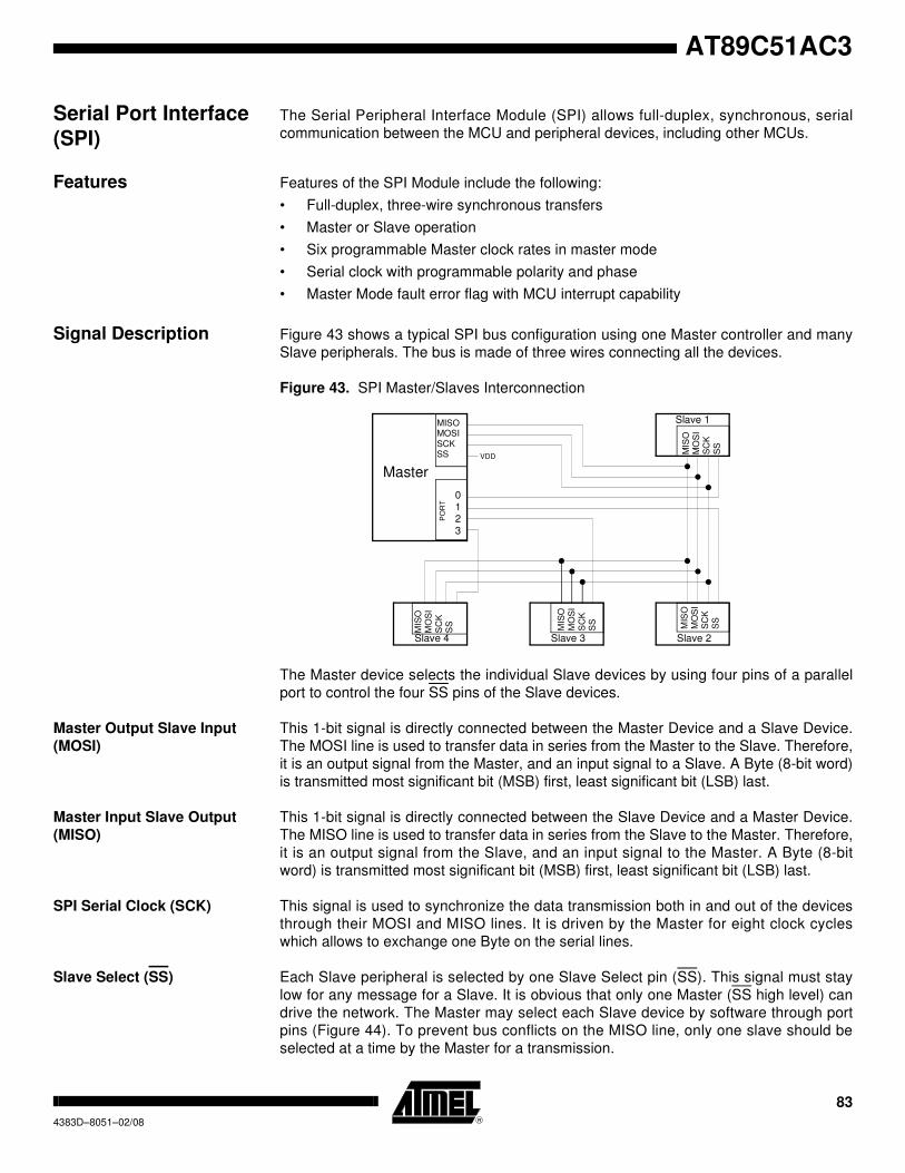
83
AT89C51AC3
4383D–8051–02/08
Serial Port Interface
(SPI)
The Serial Peripheral Interface Module (SPI) allows full-duplex, synchronous, serial
communication between the MCU and peripheral devices, including other MCUs.
Features Features of the SPI Module include the following:
• Full-duplex, three-wire synchronous transfers
• Master or Slave operation
• Six programmable Master clock rates in master mode
• Serial clock with programmable polarity and phase
• Master Mode fault error flag with MCU interrupt capability
Signal Description Figure 43 shows a typical SPI bus configuration using one Master controller and many
Slave peripherals. The bus is made of three wires connecting all the devices.
Figure 43. SPI Master/Slaves Interconnection
The Master device selects the individual Slave devices by using four pins of a parallel
port to control the four SS pins of the Slave devices.
Master Output Slave Input
(MOSI)
This 1-bit signal is directly connected between the Master Device and a Slave Device.
The MOSI line is used to transfer data in series from the Master to the Slave. Therefore,
it is an output signal from the Master, and an input signal to a Slave. A Byte (8-bit word)
is transmitted most significant bit (MSB) first, least significant bit (LSB) last.
Master Input Slave Output
(MISO)
This 1-bit signal is directly connected between the Slave Device and a Master Device.
The MISO line is used to transfer data in series from the Slave to the Master. Therefore,
it is an output signal from the Slave, and an input signal to the Master. A Byte (8-bit
word) is transmitted most significant bit (MSB) first, least significant bit (LSB) last.
SPI Serial Clock (SCK) This signal is used to synchronize the data transmission both in and out of the devices
through their MOSI and MISO lines. It is driven by the Master for eight clock cycles
which allows to exchange one Byte on the serial lines.
Slave Select (SS) Each Slave peripheral is selected by one Slave Select pin (SS). This signal must stay
low for any message for a Slave. It is obvious that only one Master (SS high level) can
drive the network. The Master may select each Slave device by software through port
pins (Figure 44). To prevent bus conflicts on the MISO line, only one slave should be
selected at a time by the Master for a transmission.
Slave 1
MIS
OM
OS
IS
CK
SS
MISOMOSISCKSS
PO
RT
0123
Slave 3
MIS
OM
OS
IS
CK
SS
Slave 4
MIS
OM
OS
IS
CK
SS
Slave 2
MIS
OM
OS
IS
CK
SS
VDD
Master
84 AT89C51AC34383D–8051–02/08
In a Master configuration, the SS line can be used in conjunction with the MODF flag in
the SPI Status register (SPSCR) to prevent multiple masters from driving MOSI and
SCK (see Error conditions).
A high level on the SS pin puts the MISO line of a Slave SPI in a high-impedance state.
The SS pin could be used as a general-purpose if the following conditions are met:
• The device is configured as a Master and the SSDIS control bit in SPCON is set.
This kind of configuration can be found when only one Master is driving the network
and there is no way that the SS pin could be pulled low. Therefore, the MODF flag in
the SPSCR will never be set(1).
• The Device is configured as a Slave with CPHA and SSDIS control bits set(2). This
kind of configuration can happen when the system includes one Master and one
Slave only. Therefore, the device should always be selected and there is no reason
that the Master uses the SS pin to select the communicating Slave device.
Note: 1. Clearing SSDIS control bit does not clear MODF.
2. Special care should be taken not to set SSDIS control bit when CPHA =’0’ because in
this mode, the SS is used to start the transmission.
Baud Rate In Master mode, the baud rate can be selected from a baud rate generator which is con-
trolled by three bits in the SPCON register: SPR2, SPR1 and SPR0.The Master clock is
selected from one of seven clock rates resulting from the division of the internal clock by
4, 8, 16, 32, 64 or 128.
Table 46 gives the different clock rates selected by SPR2:SPR1:SPR0.
In Slave mode, the maximum baud rate allowed on the SCK input is limited to Fsys/4
Table 46. SPI Master Baud Rate Selection
SPR2 SPR1 SPR0 Clock Rate Baud Rate Divisor (BD)
0 0 0 Don’t Use No BRG
0 0 1 FCLK PERIPH /4 4
0 1 0 FCLK PERIPH/8 8
0 1 1 FCLK PERIPH /16 16
1 0 0 FCLK PERIPH /32 32
1 0 1 FCLK PERIPH /64 64
1 1 0 FCLK PERIPH /128 128
1 1 1 Don’t Use No BRG
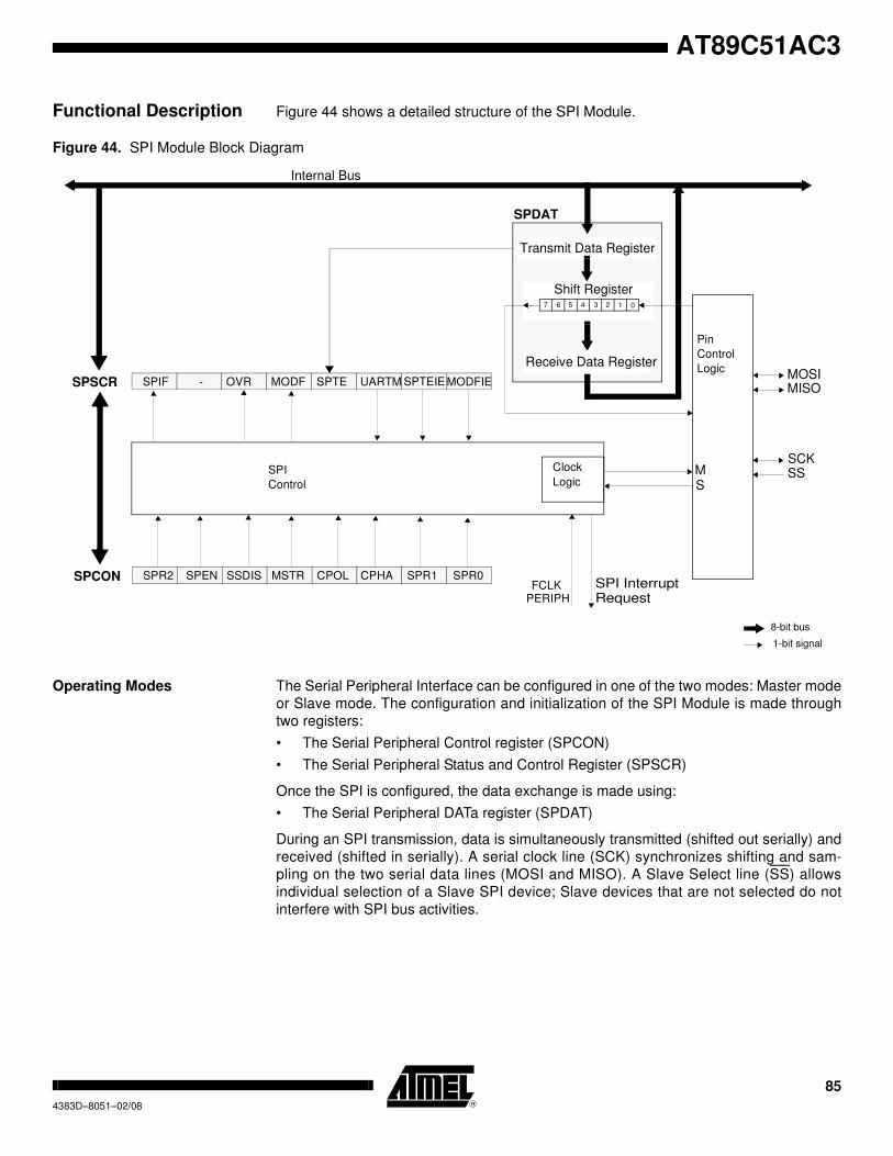
85
AT89C51AC3
4383D–8051–02/08
Functional Description Figure 44 shows a detailed structure of the SPI Module.
Figure 44. SPI Module Block Diagram
Operating Modes The Serial Peripheral Interface can be configured in one of the two modes: Master mode
or Slave mode. The configuration and initialization of the SPI Module is made through
two registers:
• The Serial Peripheral Control register (SPCON)
• The Serial Peripheral Status and Control Register (SPSCR)
Once the SPI is configured, the data exchange is made using:
• The Serial Peripheral DATa register (SPDAT)
During an SPI transmission, data is simultaneously transmitted (shifted out serially) and
received (shifted in serially). A serial clock line (SCK) synchronizes shifting and sam-
pling on the two serial data lines (MOSI and MISO). A Slave Select line (SS) allows
individual selection of a Slave SPI device; Slave devices that are not selected do not
interfere with SPI bus activities.
Shift Register01234567
Internal Bus
Pin
Control
Logic
MISOMOSI
SCKMS
Clock
Logic
SPI Interrupt
8-bit bus
1-bit signal
SS
FCLK
Receive Data Register
SPDAT
SPI
Control
Transmit Data Register
- MODFSPIF OVR SPTE UARTM SPTEIE MODFIESPSCR
SPEN MSTRSPR2 SSDIS CPOL CPHA SPR1 SPR0SPCON
Request PERIPH
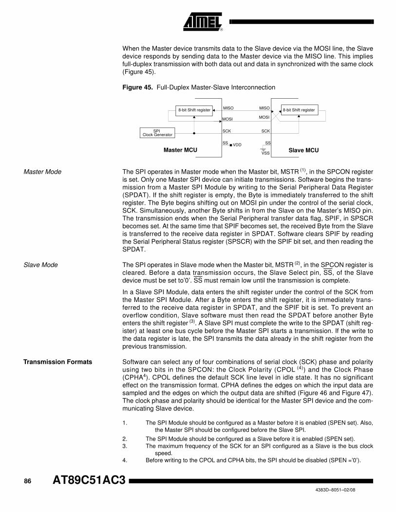
86 AT89C51AC34383D–8051–02/08
When the Master device transmits data to the Slave device via the MOSI line, the Slave
device responds by sending data to the Master device via the MISO line. This implies
full-duplex transmission with both data out and data in synchronized with the same clock
(Figure 45).
Figure 45. Full-Duplex Master-Slave Interconnection
Master Mode The SPI operates in Master mode when the Master bit, MSTR (1), in the SPCON register
is set. Only one Master SPI device can initiate transmissions. Software begins the trans-
mission from a Master SPI Module by writing to the Serial Peripheral Data Register
(SPDAT). If the shift register is empty, the Byte is immediately transferred to the shift
register. The Byte begins shifting out on MOSI pin under the control of the serial clock,
SCK. Simultaneously, another Byte shifts in from the Slave on the Master’s MISO pin.
The transmission ends when the Serial Peripheral transfer data flag, SPIF, in SPSCR
becomes set. At the same time that SPIF becomes set, the received Byte from the Slave
is transferred to the receive data register in SPDAT. Software clears SPIF by reading
the Serial Peripheral Status register (SPSCR) with the SPIF bit set, and then reading the
SPDAT.
Slave Mode The SPI operates in Slave mode when the Master bit, MSTR (2), in the SPCON register is
cleared. Before a data transmission occurs, the Slave Select pin, SS, of the Slave
device must be set to’0’. SS must remain low until the transmission is complete.
In a Slave SPI Module, data enters the shift register under the control of the SCK from
the Master SPI Module. After a Byte enters the shift register, it is immediately trans-
ferred to the receive data register in SPDAT, and the SPIF bit is set. To prevent an
overflow condition, Slave software must then read the SPDAT before another Byte
enters the shift register (3). A Slave SPI must complete the write to the SPDAT (shift reg-
ister) at least one bus cycle before the Master SPI starts a transmission. If the write to
the data register is late, the SPI transmits the data already in the shift register from the
previous transmission.
Transmission Formats Software can select any of four combinations of serial clock (SCK) phase and polarity
using two bits in the SPCON: the Clock Polarity (CPOL (4)) and the Clock Phase
(CPHA4). CPOL defines the default SCK line level in idle state. It has no significant
effect on the transmission format. CPHA defines the edges on which the input data are
sampled and the edges on which the output data are shifted (Figure 46 and Figure 47).
The clock phase and polarity should be identical for the Master SPI device and the com-
municating Slave device.
8-bit Shift register
SPI Clock Generator
Master MCU
8-bit Shift registerMISOMISO
MOSI MOSI
SCK SCK
VSS
VDD SSSS
Slave MCU
1. The SPI Module should be configured as a Master before it is enabled (SPEN set). Also,
the Master SPI should be configured before the Slave SPI.
2. The SPI Module should be configured as a Slave before it is enabled (SPEN set).
3. The maximum frequency of the SCK for an SPI configured as a Slave is the bus clock
speed.
4. Before writing to the CPOL and CPHA bits, the SPI should be disabled (SPEN =’0’).

87
AT89C51AC3
4383D–8051–02/08
Figure 46. Data Transmission Format (CPHA = 0)
Figure 47. Data Transmission Format (CPHA = 1)
Figure 48. CPHA/SS Timing
As shown in Figure 46, the first SCK edge is the MSB capture strobe. Therefore, the
Slave must begin driving its data before the first SCK edge, and a falling edge on the SS
pin is used to start the transmission. The SS pin must be toggled high and then low
between each Byte transmitted (Figure 48).
Figure 47 shows an SPI transmission in which CPHA is ’1’. In this case, the Master
begins driving its MOSI pin on the first SCK edge. Therefore, the Slave uses the first
SCK edge as a start transmission signal. The SS pin can remain low between transmis-
sions (Figure 48). This format may be preferred in systems having only one Master and
only one Slave driving the MISO data line.
Queuing transmission For an SPI configured in master or slave mode, a queued data byte must be transmit-
ted/received immediately after the previous transmission has completed.
MSB bit6 bit5 bit4 bit3 bit2 bit1 LSB
bit6 bit5 bit4 bit3 bit2 bit1MSB LSB
1 32 4 5 6 7 8
Capture Point
SS (to Slave)
MISO (from Slave)
MOSI (from Master)
SCK (CPOL = 1)
SCK (CPOL = 0)
SPEN (Internal)
SCK Cycle Number
MSB bit6 bit5 bit4 bit3 bit2 bit1 LSB
bit6 bit5 bit4 bit3 bit2 bit1MSB LSB
1 32 4 5 6 7 8
Capture Point
SS (to Slave)
MISO (from Slave)
MOSI (from Master)
SCK (CPOL = 1)
SCK (CPOL = 0)
SPEN (Internal)
SCK Cycle Number
Byte 1 Byte 2 Byte 3MISO/MOSI
Master SS
Slave SS(CPHA = 1)
Slave SS(CPHA = 0)

88 AT89C51AC34383D–8051–02/08
When a transmission is in progress a new data can be queued and sent as soon as
transmission has been completed. So it is possible to transmit bytes without latency,
useful in some applications.
The SPTE bit in SPSCR is set as long as the transmission buffer is free. It means that
the user application can write SPDAT with the data to be transmitted until the SPTE
becomes cleared.
Figure 49 shows a queuing transmission in master mode. Once the Byte 1 is ready, it is
immediately sent on the bus. Meanwhile an other byte is prepared (and the SPTE is
cleared), it will be sent at the end of the current transmission. The next data must be
ready before the end of the current transmission.
Figure 49. Queuing Transmission In Master Mode
In slave mode it is almost the same except it is the external master that start the
transmission.
Also, in slave mode, if no new data is ready, the last value received will be the next data
byte transmitted.
MSB B6 B5 B4 B3 B2 B1 LSBMOSI
SCK
MSB B6 B5 B4 B3 B2 B1 LSB
BYTE 1 under transmission
MSB B6 B5 B4 B3 B2 B1 LSB MSB B6 B5 B4 B3 B2 B1 LSBMISO
Data Byte 1 Byte 2 Byte 3
SPTE
BYTE 2 under transmission
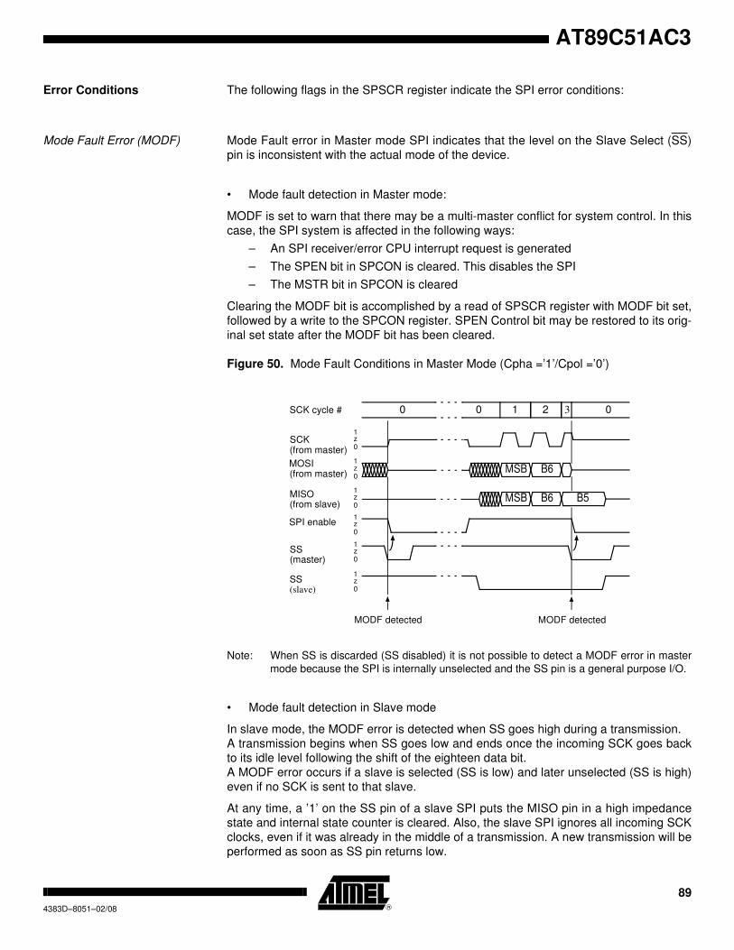
89
AT89C51AC3
4383D–8051–02/08
Error Conditions The following flags in the SPSCR register indicate the SPI error conditions:
Mode Fault Error (MODF) Mode Fault error in Master mode SPI indicates that the level on the Slave Select (SS)
pin is inconsistent with the actual mode of the device.
• Mode fault detection in Master mode:
MODF is set to warn that there may be a multi-master conflict for system control. In this
case, the SPI system is affected in the following ways:
– An SPI receiver/error CPU interrupt request is generated
– The SPEN bit in SPCON is cleared. This disables the SPI
– The MSTR bit in SPCON is cleared
Clearing the MODF bit is accomplished by a read of SPSCR register with MODF bit set,
followed by a write to the SPCON register. SPEN Control bit may be restored to its orig-
inal set state after the MODF bit has been cleared.
Figure 50. Mode Fault Conditions in Master Mode (Cpha =’1’/Cpol =’0’)
Note: When SS is discarded (SS disabled) it is not possible to detect a MODF error in master
mode because the SPI is internally unselected and the SS pin is a general purpose I/O.
• Mode fault detection in Slave mode
In slave mode, the MODF error is detected when SS goes high during a transmission.
A transmission begins when SS goes low and ends once the incoming SCK goes back
to its idle level following the shift of the eighteen data bit.
A MODF error occurs if a slave is selected (SS is low) and later unselected (SS is high)
even if no SCK is sent to that slave.
At any time, a ’1’ on the SS pin of a slave SPI puts the MISO pin in a high impedance
state and internal state counter is cleared. Also, the slave SPI ignores all incoming SCK
clocks, even if it was already in the middle of a transmission. A new transmission will be
performed as soon as SS pin returns low.
SCK
SS(master)
1 2 3SCK cycle # 0 0
SS(slave)
(from master)
MODF detected
B6MSB
B6MSB
0z1
0z1
0z1
0z1
0z1
0
0z1
SPI enable
MODF detected
MOSI
MISO
(from master)
(from slave)B5

90 AT89C51AC34383D–8051–02/08
Figure 51. Mode Fault Conditions in Slave Mode
Note: when SS is discarded (SS disabled) it is not possible to detect a MODF error in slave
mode because the SPI is internally selected. Also the SS pin becomes a general pur-
pose I/O.
OverRun Condition This error mean that the speed is not adapted for the running application:
An OverRun condition occurs when a byte has been received whereas the previous one
has not been read by the application yet.
The last byte (which generate the overrun error) does not overwrite the unread data so
that it can still be read. Therefore, an overrun error always indicates the loss of data.
Interrupts Three SPI status flags can generate a CPU interrupt requests:
Table 47. SPI Interrupts
Serial Peripheral data transfer flag, SPIF: This bit is set by hardware when a transfer
has been completed. SPIF bit generates transmitter CPU interrupt request only when
SPTEIE is disabled.
Mode Fault flag, MODF: This bit is set to indicate that the level on the SS is inconsistent
with the mode of the SPI (in both master and slave modes).
Serial Peripheral Transmit Register empty flag, SPTE: This bit is set when the transmit
buffer is empty (other data can be loaded is SPDAT). SPTE bit generates transmitter
CPU interrupt request only when SPTEIE is enabled.
Note: While using SPTE interruption for “burst mode” transfers (SPTEIE=’1’), the
user software application should take care to clear SPTEIE, during the last but one
data reception (to be able to generate an interrupt on SPIF flag at the end of the last
data reception).
SCK
1 2 3SCK cycle # 0
SS(slave)
(from master)
MODF detected
B6MSB
B6MSB
0z1
0z1
0z1
0z1
0
MODF detected
MOSI
MISO
(from master)
(from slave)MSB
B5 B4
4
Flag Request
SPIF (SPI data transfer) SPI Transmitter Interrupt Request
MODF (Mode Fault) SPI mode-fault Interrupt Request
SPTE (Transmit register empty) SPI transmit register empty Interrupt Request

91
AT89C51AC3
4383D–8051–02/08
Figure 52. SPI Interrupt Requests Generation
Registers Three registers in the SPI module provide control, status and data storage functions.
These registers are describe in the following paragraphs.
Serial Peripheral Control
Register (SPCON)
• The Serial Peripheral Control Register does the following:
• Selects one of the Master clock rates
• Configure the SPI Module as Master or Slave
• Selects serial clock polarity and phase
• Enables the SPI Module
• Frees the SS pin for a general-purpose
Table 48 describes this register and explains the use of each bit
Table 48. SPCON Register
SPCON - Serial Peripheral Control Register (0D4H)
SPI
CPU Interrupt Request
SPIF
SPTEIE
SPTE
MODF
MODFIE
7 6 5 4 3 2 1 0
SPR2 SPEN SSDIS MSTR CPOL CPHA SPR1 SPR0
Bit Number Bit Mnemonic Description
7 SPR2
Serial Peripheral Rate 2
Bit with SPR1 and SPR0 define the clock rate (See bits SPR1 and
SPR0 for detail).
6 SPEN
Serial Peripheral Enable
Cleared to disable the SPI interface (internal reset of the SPI).
Set to enable the SPI interface.
5 SSDIS
SS Disable
Cleared to enable SS in both Master and Slave modes.
Set to disable SS in both Master and Slave modes. In Slave mode,
this bit has no effect if CPHA =’0’. When SSDIS is set, no MODF
interrupt request is generated.
4 MSTR
Serial Peripheral Master
Cleared to configure the SPI as a Slave.
Set to configure the SPI as a Master.

92 AT89C51AC34383D–8051–02/08
Reset Value = 0001 0100b
Not bit addressable
Serial Peripheral Status Register
and Control (SPSCR)
The Serial Peripheral Status Register contains flags to signal the following conditions:
• Data transfer complete
• Write collision
• Inconsistent logic level on SS pin (mode fault error)
Table 49. SPSCR Register
SPSCR - Serial Peripheral Status and Control register (0D5H)
3 CPOL
Clock Polarity
Cleared to have the SCK set to ’0’ in idle state.
Set to have the SCK set to ’1’ in idle state.
2 CPHA
Clock Phase
Cleared to have the data sampled when the SCK leaves the idle
state (see CPOL).
Set to have the data sampled when the SCK returns to idle state (see
CPOL).
1 SPR1
SPR2 SPR1 SPR0 Serial Peripheral Rate
0 0 0 Invalid
0 0 1 FCLK PERIPH /4
0 1 0 FCLK PERIPH /8
0 1 1 FCLK PERIPH /16
1 0 0 FCLK PERIPH /32
1 0 1 FCLK PERIPH /64
1 1 0 FCLK PERIPH /128
1 1 1 Invalid
0 SPR0
Bit Number Bit Mnemonic Description
7 6 5 4 3 2 1 0
SPIF - OVR MODF SPTE UARTM SPTEIE MODFIE
Bit
Number
Bit
Mnemonic Description
7 SPIF
Serial Peripheral Data Transfer Flag
Cleared by hardware to indicate data transfer is in progress or has been
approved by a clearing sequence.
Set by hardware to indicate that the data transfer has been completed.
This bit is cleared when reading or writing SPDATA after reading SPSCR.
6 -Reserved
The value read from this bit is indeterminate. Do not set this bit.
5 OVR
Overrun Error Flag
- Set by hardware when a byte is received whereas SPIF is set (the previous
received data is not overwritten).
- Cleared by hardware when reading SPSCR

93
AT89C51AC3
4383D–8051–02/08
Reset Value = 00X0 XXXXb
Not Bit addressable
4 MODF
Mode Fault
- Set by hardware to indicate that the SS pin is in inappropriate logic level (in both
master and slave modes).
- Cleared by hardware when reading SPSCR
When MODF error occurred:
- In slave mode: SPI interface ignores all transmitted data while SS remains high.
A new transmission is perform as soon as SS returns low.
- In master mode: SPI interface is disabled (SPEN=0, see description for SPEN
bit in SPCON register).
3 SPTE
Serial Peripheral Transmit register Empty
- Set by hardware when transmit register is empty (if needed, SPDAT can be
loaded with another data).
- Cleared by hardware when transmit register is full (no more data should be
loaded in SPDAT).
2 UARTM
Serial Peripheral UART mode
Set and cleared by software:
- Clear: Normal mode, data are transmitted MSB first (default)
- Set: UART mode, data are transmitted LSB first.
1 SPTEIE
Interrupt Enable for SPTE
Set and cleared by software:
- Set to enable SPTE interrupt generation (when SPTE goes high, an interrupt is
generated).
- Clear to disable SPTE interrupt generation
Caution: When SPTEIE is set no interrupt generation occurred when SPIF flag
goes high. To enable SPIF interrupt again, SPTEIE should be cleared.
0 MODFIE
Interrupt Enable for MODF
Set and cleared by software:
- Set to enable MODF interrupt generation
- Clear to disable MODF interrupt generation
Bit
Number
Bit
Mnemonic Description
94 AT89C51AC34383D–8051–02/08
Programmable
Counter Array (PCA)
The PCA provides more timing capabilities with less CPU intervention than the standard
timer/counters. Its advantages include reduced software overhead and improved accu-
racy. The PCA consists of a dedicated timer/counter which serves as the time base for
an array of five compare/capture modules. Its clock input can be programmed to count
any of the following signals:
• PCA clock frequency/6 (see “clock” section)
• PCA clock frequency/2
• Timer 0 overflow
• External input on ECI (P1.2)
Each compare/capture modules can be programmed in any one of the following modes:
• rising and/or falling edge capture,
• software timer,
• high-speed output,
• pulse width modulator.
Module 4 can also be programmed as a WatchDog timer. see the "PCA WatchDog
Timer" section.
When the compare/capture modules are programmed in capture mode, software timer,
or high speed output mode, an interrupt can be generated when the module executes its
function. All five modules plus the PCA timer overflow share one interrupt vector.
The PCA timer/counter and compare/capture modules share Port 1 for external I/Os.
These pins are listed below. If the port is not used for the PCA, it can still be used for
standard I/O.
PCA Timer The PCA timer is a common time base for all five modules (see Figure 53). The timer
count source is determined from the CPS1 and CPS0 bits in the CMOD SFR (see Table
8) and can be programmed to run at:
• 1/6 the PCA clock frequency.
• 1/2 the PCA clock frequency.
• the Timer 0 overflow.
• the input on the ECI pin (P1.2).
PCA Component External I/O Pin
16-bit Counter P1.2/ECI
16-bit Module 0 P1.3/CEX0
16-bit Module 1 P1.4/CEX1
16-bit Module 2 P1.5/CEX2
16-bit Module 3 P1.6/CEX3
16-bit Module 4 P1.7/CEX4

95
AT89C51AC3
4383D–8051–02/08
Figure 53. PCA Timer/Counter
The CMOD register includes three additional bits associated with the PCA.
• The CIDL bit which allows the PCA to stop during idle mode.
• The WDTE bit which enables or disables the WatchDog function on module 4.
• The ECF bit which when set causes an interrupt and the PCA overflow flag CF in
CCON register to be set when the PCA timer overflows.
The CCON register contains the run control bit for the PCA and the flags for the PCA
timer and each module.
• The CR bit must be set to run the PCA. The PCA is shut off by clearing this bit.
• The CF bit is set when the PCA counter overflows and an interrupt will be generated
if the ECF bit in CMOD register is set. The CF bit can only be cleared by software.
• The CCF0:4 bits are the flags for the modules (CCF0 for module0...) and are set by
hardware when either a match or a capture occurs. These flags also can be cleared
by software.
PCA Modules Each one of the five compare/capture modules has six possible functions. It can
perform:
• 16-bit Capture, positive-edge triggered
• 16-bit Capture, negative-edge triggered
• 16-bit Capture, both positive and negative-edge triggered
• 16-bit Software Timer
• 16-bit High Speed Output
• 8-bit Pulse Width Modulator.
In addition module 4 can be used as a WatchDog Timer.
CIDL CPS1 CPS0 ECF
ItCH CL
16 bit up counter
To PCAmodules
FPca/6
FPca/2
T0 OVF
P1.2
Idle
CMOD0xD9WDTE
CF CRCCON0xD8CCF4 CCF3 CCF2 CCF1 CCF0
overflow
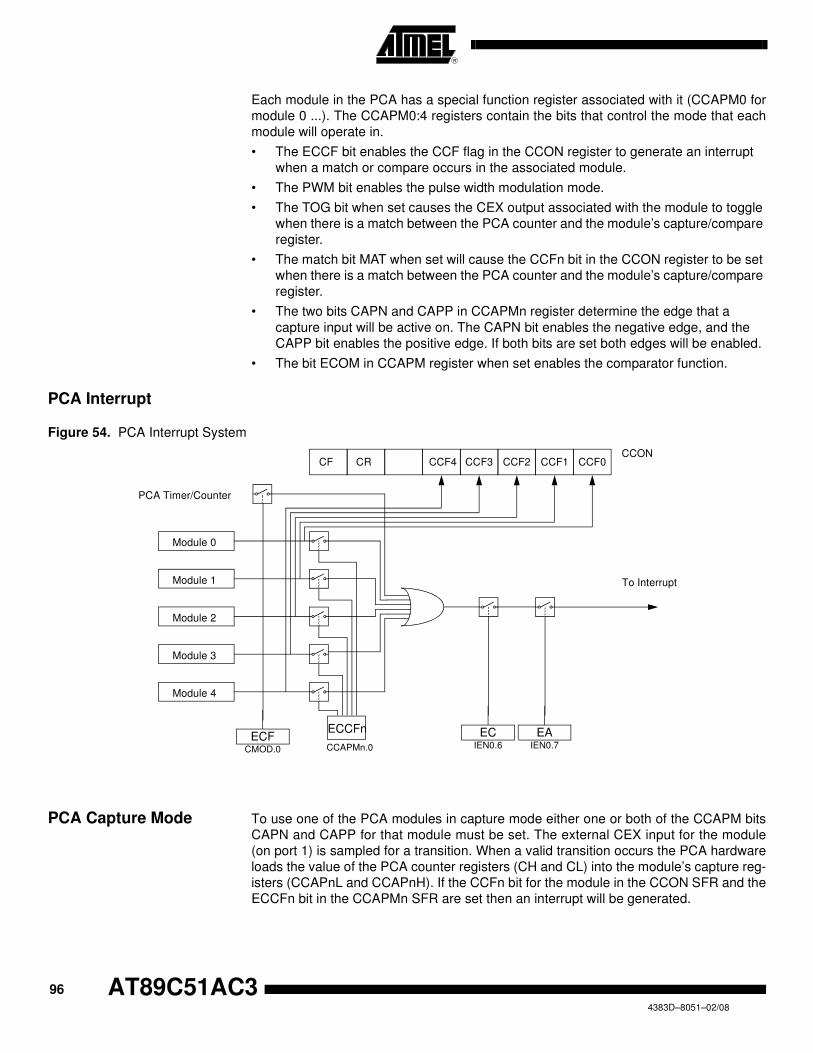
96 AT89C51AC34383D–8051–02/08
Each module in the PCA has a special function register associated with it (CCAPM0 for
module 0 ...). The CCAPM0:4 registers contain the bits that control the mode that each
module will operate in.
• The ECCF bit enables the CCF flag in the CCON register to generate an interrupt
when a match or compare occurs in the associated module.
• The PWM bit enables the pulse width modulation mode.
• The TOG bit when set causes the CEX output associated with the module to toggle
when there is a match between the PCA counter and the module’s capture/compare
register.
• The match bit MAT when set will cause the CCFn bit in the CCON register to be set
when there is a match between the PCA counter and the module’s capture/compare
register.
• The two bits CAPN and CAPP in CCAPMn register determine the edge that a
capture input will be active on. The CAPN bit enables the negative edge, and the
CAPP bit enables the positive edge. If both bits are set both edges will be enabled.
• The bit ECOM in CCAPM register when set enables the comparator function.
PCA Interrupt
Figure 54. PCA Interrupt System
PCA Capture Mode To use one of the PCA modules in capture mode either one or both of the CCAPM bits
CAPN and CAPP for that module must be set. The external CEX input for the module
(on port 1) is sampled for a transition. When a valid transition occurs the PCA hardware
loads the value of the PCA counter registers (CH and CL) into the module’s capture reg-
isters (CCAPnL and CCAPnH). If the CCFn bit for the module in the CCON SFR and the
ECCFn bit in the CCAPMn SFR are set then an interrupt will be generated.
CF CRCCON
CCF4 CCF3 CCF2 CCF1 CCF0
Module 4
Module 3
Module 2
Module 1
Module 0
PCA Timer/Counter
ECCFn
CCAPMn.0
To Interrupt
EAIEN0.7
ECIEN0.6
ECFCMOD.0

97
AT89C51AC3
4383D–8051–02/08
Figure 55. PCA Capture Mode
16-bit Software Timer Mode
The PCA modules can be used as software timers by setting both the ECOM and MAT
bits in the modules CCAPMn register. The PCA timer will be compared to the module’s
capture registers and when a match occurs an interrupt will occur if the CCFn (CCON
SFR) and the ECCFn (CCAPMn SFR) bits for the module are both set.
Figure 56. PCA 16-bit Software Timer and High Speed Output Mode
CEXn
n = 0, 4
PCA Counter
CH(8bits)
CL(8bits)
CCAPnH CCAPnL
CCFn
CCON
PCA
Interrupt
Request
- 0CAPPn CAPNn 000 ECCFn
7
CCAPMn Register (n = 0, 4)0
CCAPnL(8 bits)
CCAPnH(8 bits)
- ECOMn0 0 MATn TOGn0 ECCFn
7 0
CCAPMn Register
(n = 0, 4)
CH(8 bits)
CL(8 bits)
16-Bit ComparatorMatch
EnableCCFn
CCON reg
PCA
Interrupt
Request
CEXn
Compare/Capture ModulePCA Counter
“0”
“1”
Reset
Write to
CCAPnL
Write to CCAPnH
For software Timer mode, set ECOMn and MATn.
For high speed output mode, set ECOMn, MATn and TOGn.
Toggle
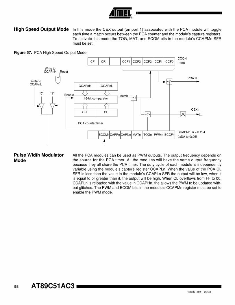
98 AT89C51AC34383D–8051–02/08
High Speed Output Mode In this mode the CEX output (on port 1) associated with the PCA module will toggle
each time a match occurs between the PCA counter and the module’s capture registers.
To activate this mode the TOG, MAT, and ECOM bits in the module’s CCAPMn SFR
must be set.
Figure 57. PCA High Speed Output Mode
Pulse Width Modulator Mode
All the PCA modules can be used as PWM outputs. The output frequency depends on
the source for the PCA timer. All the modules will have the same output frequency
because they all share the PCA timer. The duty cycle of each module is independently
variable using the module’s capture register CCAPLn. When the value of the PCA CL
SFR is less than the value in the module’s CCAPLn SFR the output will be low, when it
is equal to or greater than it, the output will be high. When CL overflows from FF to 00,
CCAPLn is reloaded with the value in CCAPHn. the allows the PWM to be updated with-
out glitches. The PWM and ECOM bits in the module’s CCAPMn register must be set to
enable the PWM mode.
CH CL
CCAPnH CCAPnL
ECOMnCCAPMn, n = 0 to 4
0xDA to 0xDECAPNn MATn TOGn PWMn ECCFnCAPPn
16-bit comparatorMatch
CF CRCCON
0xD8CCF4 CCF3 CCF2 CCF1 CCF0
PCA IT
Enable
CEXn
PCA counter/timer
“1”“0”
Write toCCAPnL
ResetWrite to
CCAPnH
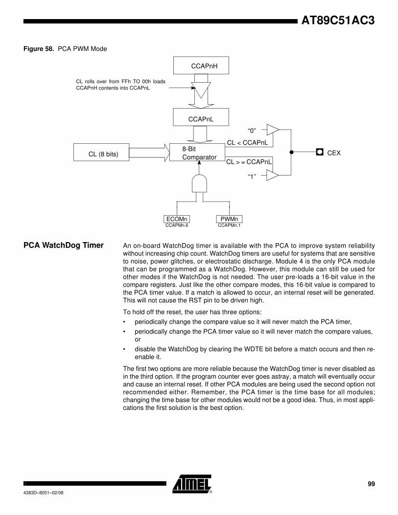
99
AT89C51AC3
4383D–8051–02/08
Figure 58. PCA PWM Mode
PCA WatchDog Timer An on-board WatchDog timer is available with the PCA to improve system reliability
without increasing chip count. WatchDog timers are useful for systems that are sensitive
to noise, power glitches, or electrostatic discharge. Module 4 is the only PCA module
that can be programmed as a WatchDog. However, this module can still be used for
other modes if the WatchDog is not needed. The user pre-loads a 16-bit value in the
compare registers. Just like the other compare modes, this 16-bit value is compared to
the PCA timer value. If a match is allowed to occur, an internal reset will be generated.
This will not cause the RST pin to be driven high.
To hold off the reset, the user has three options:
• periodically change the compare value so it will never match the PCA timer,
• periodically change the PCA timer value so it will never match the compare values,
or
• disable the WatchDog by clearing the WDTE bit before a match occurs and then re-
enable it.
The first two options are more reliable because the WatchDog timer is never disabled as
in the third option. If the program counter ever goes astray, a match will eventually occur
and cause an internal reset. If other PCA modules are being used the second option not
recommended either. Remember, the PCA timer is the time base for all modules;
changing the time base for other modules would not be a good idea. Thus, in most appli-
cations the first solution is the best option.
CL rolls over from FFh TO 00h loads
CCAPnH contents into CCAPnL
CCAPnL
CCAPnH
8-Bit
ComparatorCL (8 bits)
“0”
“1”
CL < CCAPnL
CL > = CCAPnL
CEX
PWMnCCAPMn.1
ECOMnCCAPMn.6

100 AT89C51AC34383D–8051–02/08
PCA Registers Table 50. CMOD Register
CMOD (S:D9h)
PCA Counter Mode Register
Reset Value = 00XX X000b
7 6 5 4 3 2 1 0
CIDL WDTE - - - CPS1 CPS0 ECF
Bit
Number
Bit
Mnemonic Description
7 CIDL
PCA Counter Idle Control bit
Clear to let the PCA run during Idle mode.
Set to stop the PCA when Idle mode is invoked.
6 WDTE
WatchDog Timer Enable
Clear to disable WatchDog Timer function on PCA Module 4,
Set to enable it.
5 -Reserved
The value read from this bit is indeterminate. Do not set this bit.
4 -Reserved
The value read from this bit is indeterminate. Do not set this bit.
3 -Reserved
The value read from this bit is indeterminate. Do not set this bit.
2-1 CPS1:0
EWC Count Pulse Select bits
CPS1 CPS0 Clock source
0 0 Internal Clock, FPca/6
0 1 Internal Clock, FPca/2
1 0 Timer 0 overflow
1 1 External clock at ECI/P1.2 pin (Max. Rate = FPca/4)
0 ECF
Enable PCA Counter Overflow Interrupt bit
Clear to disable CF bit in CCON register to generate an interrupt.
Set to enable CF bit in CCON register to generate an interrupt.
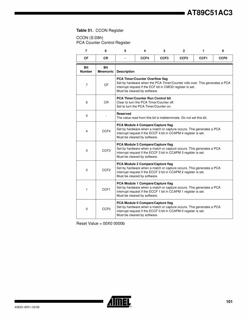
101
AT89C51AC3
4383D–8051–02/08
Table 51. CCON Register
CCON (S:D8h)
PCA Counter Control Register
Reset Value = 00X0 0000b
7 6 5 4 3 2 1 0
CF CR - CCF4 CCF3 CCF2 CCF1 CCF0
Bit
Number
Bit
Mnemonic Description
7 CF
PCA Timer/Counter Overflow flag
Set by hardware when the PCA Timer/Counter rolls over. This generates a PCA
interrupt request if the ECF bit in CMOD register is set.
Must be cleared by software.
6 CR
PCA Timer/Counter Run Control bit
Clear to turn the PCA Timer/Counter off.
Set to turn the PCA Timer/Counter on.
5 -Reserved
The value read from this bit is indeterminate. Do not set this bit.
4 CCF4
PCA Module 4 Compare/Capture flag
Set by hardware when a match or capture occurs. This generates a PCA
interrupt request if the ECCF 4 bit in CCAPM 4 register is set.
Must be cleared by software.
3 CCF3
PCA Module 3 Compare/Capture flag
Set by hardware when a match or capture occurs. This generates a PCA
interrupt request if the ECCF 3 bit in CCAPM 3 register is set.
Must be cleared by software.
2 CCF2
PCA Module 2 Compare/Capture flag
Set by hardware when a match or capture occurs. This generates a PCA
interrupt request if the ECCF 2 bit in CCAPM 2 register is set.
Must be cleared by software.
1 CCF1
PCA Module 1 Compare/Capture flag
Set by hardware when a match or capture occurs. This generates a PCA
interrupt request if the ECCF 1 bit in CCAPM 1 register is set.
Must be cleared by software.
0 CCF0
PCA Module 0 Compare/Capture flag
Set by hardware when a match or capture occurs. This generates a PCA
interrupt request if the ECCF 0 bit in CCAPM 0 register is set.
Must be cleared by software.

102 AT89C51AC34383D–8051–02/08
Table 52. CCAPnH Registers
CCAP0H (S:FAh)
CCAP1H (S:FBh)
CCAP2H (S:FCh)
CCAP3H (S:FDh)
CCAP4H (S:FEh)
PCA High Byte Compare/Capture Module n Register (n=0..4)
Reset Value = 0000 0000b
Table 53. CCAPnL Registers
CCAP0L (S:EAh)
CCAP1L (S:EBh)
CCAP2L (S:ECh)
CCAP3L (S:EDh)
CCAP4L (S:EEh)
PCA Low Byte Compare/Capture Module n Register (n=0..4)
Reset Value = 0000 0000b
7 6 5 4 3 2 1 0
CCAPnH 7 CCAPnH 6 CCAPnH 5 CCAPnH 4 CCAPnH 3 CCAPnH 2 CCAPnH 1 CCAPnH 0
Bit
Number
Bit
Mnemonic Description
7:0CCAPnH
7:0High byte of EWC-PCA comparison or capture values
7 6 5 4 3 2 1 0
CCAPnL 7 CCAPnL 6 CCAPnL 5 CCAPnL 4 CCAPnL 3 CCAPnL 2 CCAPnL 1 CCAPnL 0
Bit
Number
Bit
Mnemonic Description
7:0CCAPnL
7:0Low byte of EWC-PCA comparison or capture values

103
AT89C51AC3
4383D–8051–02/08
Table 54. CCAPMn Registers
CCAPM0 (S:DAh)
CCAPM1 (S:DBh)
CCAPM2 (S:DCh)
CCAPM3 (S:DDh)
CCAPM4 (S:DEh)
PCA Compare/Capture Module n Mode registers (n=0..4)
Reset Value = X000 0000b
7 6 5 4 3 2 1 0
- ECOMn CAPPn CAPNn MATn TOGn PWMn ECCFn
Bit
Number
Bit
Mnemonic Description
7 -Reserved
The Value read from this bit is indeterminate. Do not set this bit.
6 ECOMn
Enable Compare Mode Module x bit
Clear to disable the Compare function.
Set to enable the Compare function.
The Compare function is used to implement the software Timer, the high-speed
output, the Pulse Width Modulator (PWM) and the WatchDog Timer (WDT).
5 CAPPn
Capture Mode (Positive) Module x bit
Clear to disable the Capture function triggered by a positive edge on CEXx pin.
Set to enable the Capture function triggered by a positive edge on CEXx pin
4 CAPNn
Capture Mode (Negative) Module x bit
Clear to disable the Capture function triggered by a negative edge on CEXx pin.
Set to enable the Capture function triggered by a negative edge on CEXx pin.
3 MATn
Match Module x bit
Set when a match of the PCA Counter with the Compare/Capture register sets
CCFx bit in CCON register, flagging an interrupt.
2 TOGn
Toggle Module x bit
The toggle mode is configured by setting ECOMx, MATx and TOGx bits.
Set when a match of the PCA Counter with the Compare/Capture register
toggles the CEXx pin.
1 PWMn
Pulse Width Modulation Module x Mode bit
Set to configure the module x as an 8-bit Pulse Width Modulator with output
waveform on CEXx pin.
0 ECCFn
Enable CCFx Interrupt bit
Clear to disable CCFx bit in CCON register to generate an interrupt request.
Set to enable CCFx bit in CCON register to generate an interrupt request.
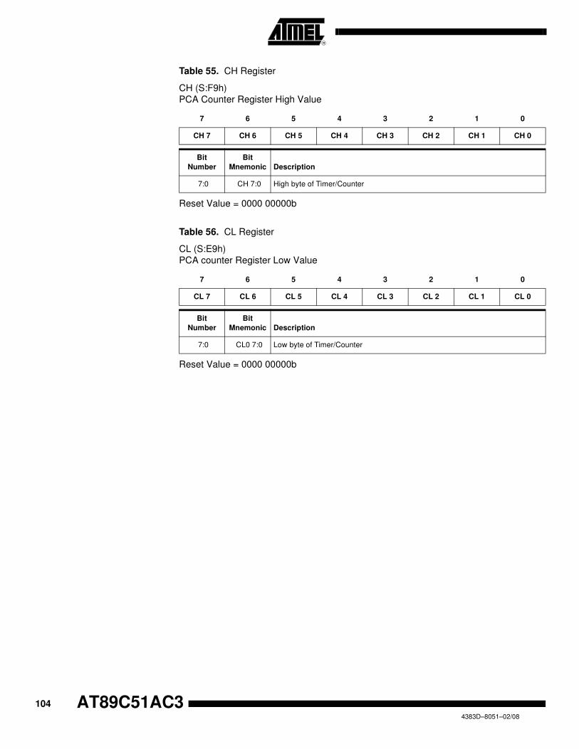
104 AT89C51AC34383D–8051–02/08
Table 55. CH Register
CH (S:F9h)
PCA Counter Register High Value
Reset Value = 0000 00000b
Table 56. CL Register
CL (S:E9h)
PCA counter Register Low Value
Reset Value = 0000 00000b
7 6 5 4 3 2 1 0
CH 7 CH 6 CH 5 CH 4 CH 3 CH 2 CH 1 CH 0
Bit
Number
Bit
Mnemonic Description
7:0 CH 7:0 High byte of Timer/Counter
7 6 5 4 3 2 1 0
CL 7 CL 6 CL 5 CL 4 CL 3 CL 2 CL 1 CL 0
Bit
Number
Bit
Mnemonic Description
7:0 CL0 7:0 Low byte of Timer/Counter
105
AT89C51AC3
4383D–8051–02/08
Analog-to-Digital
Converter (ADC)
This section describes the on-chip 10 bit analog-to-digital converter of the
AT89C51AC3. Eight ADC channels are available for sampling of the external sources
AN0 to AN7. An analog multiplexer allows the single ADC converter to select one from
the 8 ADC channels as ADC input voltage (ADCIN). ADCIN is converted by the 10-bit
cascaded potentiometric ADC.
Two kinds of conversion are available:
- Standard conversion (8 bits).
- Precision conversion (10 bits).
For the precision conversion, set bit PSIDLE in ADCON register and start conversion.
The device is in a pseudo-idle mode, the CPU does not run but the peripherals are
always running. This mode allows digital noise to be as low as possible, to ensure high
precision conversion.
For this mode it is necessary to work with end of conversion interrupt, which is the only
way to wake the device up.
If another interrupt occurs during the precision conversion, it will be treated only after
this conversion is ended.
Features • 8 channels with multiplexed inputs
• 10-bit cascaded potentiometric ADC
• Conversion time 16 micro-seconds (typ.)
• Zero Error (offset) ± 2 LSB max
• Positive External Reference Voltage Range (VREF) 2.4 to 3.0Volt (typ.)
• ADCIN Range 0 to 3Volt
• Integral non-linearity typical 1 LSB, max. 2 LSB
• Differential non-linearity typical 0.5 LSB, max. 1 LSB
• Conversion Complete Flag or Conversion Complete Interrupt
• Selectable ADC Clock
ADC Port1 I/O Functions Port 1 pins are general I/O that are shared with the ADC channels. The channel select
bit in ADCF register define which ADC channel/port1 pin will be used as ADCIN. The
remaining ADC channels/port1 pins can be used as general-purpose I/O or as the alter-
nate function that is available.
A conversion launched on a channel which are not selected on ADCF register will not
have any effect.

106 AT89C51AC34383D–8051–02/08
Figure 59. ADC Description
Figure 60 shows the timing diagram of a complete conversion. For simplicity, the figure
depicts the waveforms in idealized form and do not provide precise timing information.
For ADC characteristics and timing parameters refer to the Section “AC Characteristics”
of the AT89C51AC3 datasheet.
Figure 60. Timing Diagram
Note: Tsetup min = 4 us
Tconv=11 clock ADC = 1sample and hold + 10 bit conversion
The user must ensure that 4 us minimum time between setting ADEN and the start of the first conversion.
AN0/P1.0
AN1/P1.1
AN2/P1.2
AN3/P1.3
AN4/P1.4
AN5/P1.5
AN6/P1.6
AN7/P1.7
000
001
010
011
100
101
110
111
SCH2ADCON.2
SCH0ADCON.0
SCH1ADCON.1
ADCCLOCK
ADENADCON.5
ADSSTADCON.3
ADEOCADCON.4 ADC
InterruptRequest
EADCIEN1.1
CONTROL
AVSS
Sample and Hold
ADDH
VAREF
R/2R DAC
VAGND
8
10
+
-
ADDL2SAR
ADCIN
ADEN
ADSST
ADEOC
TSETUP
TCONV
CLK
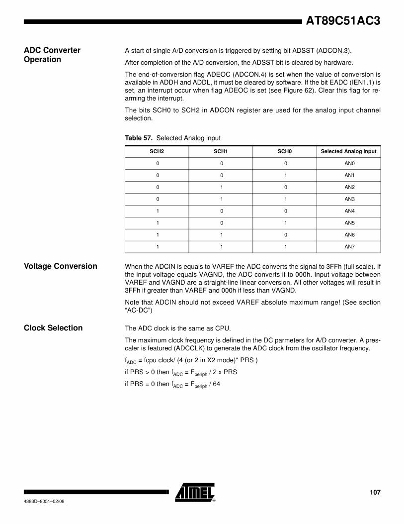
107
AT89C51AC3
4383D–8051–02/08
ADC Converter Operation
A start of single A/D conversion is triggered by setting bit ADSST (ADCON.3).
After completion of the A/D conversion, the ADSST bit is cleared by hardware.
The end-of-conversion flag ADEOC (ADCON.4) is set when the value of conversion is
available in ADDH and ADDL, it must be cleared by software. If the bit EADC (IEN1.1) is
set, an interrupt occur when flag ADEOC is set (see Figure 62). Clear this flag for re-
arming the interrupt.
The bits SCH0 to SCH2 in ADCON register are used for the analog input channel
selection.
Table 57. Selected Analog input
Voltage Conversion When the ADCIN is equals to VAREF the ADC converts the signal to 3FFh (full scale). If
the input voltage equals VAGND, the ADC converts it to 000h. Input voltage between
VAREF and VAGND are a straight-line linear conversion. All other voltages will result in
3FFh if greater than VAREF and 000h if less than VAGND.
Note that ADCIN should not exceed VAREF absolute maximum range! (See section
“AC-DC”)
Clock Selection The ADC clock is the same as CPU.
The maximum clock frequency is defined in the DC parmeters for A/D converter. A pres-
caler is featured (ADCCLK) to generate the ADC clock from the oscillator frequency.
fADC = fcpu clock/ (4 (or 2 in X2 mode)* PRS )
if PRS > 0 then fADC = Fperiph / 2 x PRS
if PRS = 0 then fADC = Fperiph / 64
SCH2 SCH1 SCH0 Selected Analog input
0 0 0 AN0
0 0 1 AN1
0 1 0 AN2
0 1 1 AN3
1 0 0 AN4
1 0 1 AN5
1 1 0 AN6
1 1 1 AN7
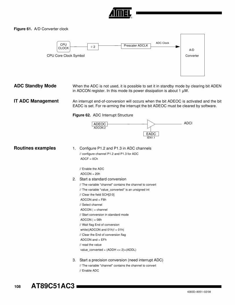
108 AT89C51AC34383D–8051–02/08
Figure 61. A/D Converter clock
ADC Standby Mode When the ADC is not used, it is possible to set it in standby mode by clearing bit ADEN
in ADCON register. In this mode its power dissipation is about 1 µW.
IT ADC Management An interrupt end-of-conversion will occurs when the bit ADEOC is activated and the bit
EADC is set. For re-arming the interrupt the bit ADEOC must be cleared by software.
Figure 62. ADC Interrupt Structure
Routines examples 1. Configure P1.2 and P1.3 in ADC channels
// configure channel P1.2 and P1.3 for ADC
ADCF = 0Ch
// Enable the ADC
ADCON = 20h
2. Start a standard conversion
// The variable "channel" contains the channel to convert
// The variable "value_converted" is an unsigned int
// Clear the field SCH[2:0]
ADCON and = F8h
// Select channel
ADCON | = channel
// Start conversion in standard mode
ADCON | = 08h
// Wait flag End of conversion
while((ADCON and 01h)! = 01h)
// Clear the End of conversion flag
ADCON and = EFh
// read the value
value_converted = (ADDH << 2)+(ADDL)
3. Start a precision conversion (need interrupt ADC)
// The variable "channel" contains the channel to convert
// Enable ADC
Prescaler ADCLK
A/D
Converter
ADC ClockCPU
CLOCK
CPU Core Clock Symbol
÷ 2
ADEOCADCON.2
EADCIEN1.1
ADCI

109
AT89C51AC3
4383D–8051–02/08
EADC = 1
// clear the field SCH[2:0]
ADCON and = F8h
// Select the channel
ADCON | = channel
// Start conversion in precision mode
ADCON | = 48h
Note: to enable the ADC interrupt:
EA = 1

110 AT89C51AC34383D–8051–02/08
Registers Table 58. ADCF Register
ADCF (S:F6h)
ADC Configuration
Reset Value =0000 0000b
Table 59. ADCON Register
ADCON (S:F3h)
ADC Control Register
Reset Value =X000 0000b
7 6 5 4 3 2 1 0
CH 7 CH 6 CH 5 CH 4 CH 3 CH 2 CH 1 CH 0
Bit
Number
Bit
Mnemonic Description
7-0 CH 0:7
Channel Configuration
Set to use P1.x as ADC input.
Clear to use P1.x as standart I/O port.
7 6 5 4 3 2 1 0
- PSIDLE ADEN ADEOC ADSST SCH2 SCH1 SCH0
Bit
Number
Bit
Mnemonic Description
7 -
6 PSIDLE
Pseudo Idle Mode (Best Precision)
Set to put in idle mode during conversion
Clear to convert without idle mode.
5 ADEN
Enable/Standby Mode
Set to enable ADC
Clear for Standby mode (power dissipation 1 uW).
4 ADEOC
End Of Conversion
Set by hardware when ADC result is ready to be read. This flag can generate an
interrupt.
Must be cleared by software.
3 ADSST
Start and Status
Set to start an A/D conversion.
Cleared by hardware after completion of the conversion
2-0 SCH2:0Selection of Channel to Convert
see Table 57
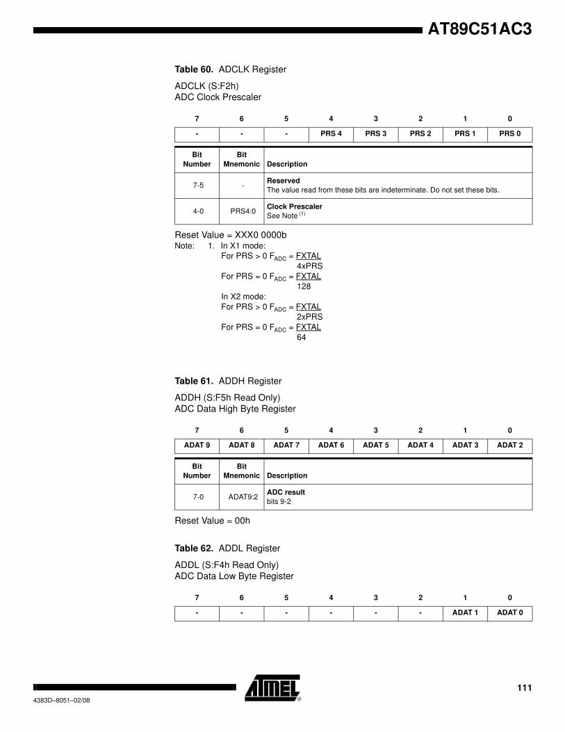
111
AT89C51AC3
4383D–8051–02/08
Table 60. ADCLK Register
ADCLK (S:F2h)
ADC Clock Prescaler
Reset Value = XXX0 0000bNote: 1. In X1 mode:
For PRS > 0 FADC = FXTAL
4xPRS
For PRS = 0 FADC = FXTAL
128
In X2 mode:
For PRS > 0 FADC = FXTAL
2xPRS
For PRS = 0 FADC = FXTAL
64
Table 61. ADDH Register
ADDH (S:F5h Read Only)
ADC Data High Byte Register
Reset Value = 00h
Table 62. ADDL Register
ADDL (S:F4h Read Only)
ADC Data Low Byte Register
7 6 5 4 3 2 1 0
- - - PRS 4 PRS 3 PRS 2 PRS 1 PRS 0
Bit
Number
Bit
Mnemonic Description
7-5 -Reserved
The value read from these bits are indeterminate. Do not set these bits.
4-0 PRS4:0Clock Prescaler
See Note (1)
7 6 5 4 3 2 1 0
ADAT 9 ADAT 8 ADAT 7 ADAT 6 ADAT 5 ADAT 4 ADAT 3 ADAT 2
Bit
Number
Bit
Mnemonic Description
7-0 ADAT9:2ADC result
bits 9-2
7 6 5 4 3 2 1 0
- - - - - - ADAT 1 ADAT 0

112 AT89C51AC34383D–8051–02/08
Reset Value = 00h
Bit
Number
Bit
Mnemonic Description
7-2 -Reserved
The value read from these bits are indeterminate. Do not set these bits.
1-0 ADAT1:0ADC result
bits 1-0

113
AT89C51AC3
4383D–8051–02/08
Interrupt System
Introduction The Micro-controller has a total of 9 interrupt vectors: two external interrupts (INT0 and
INT1), three timer interrupts (timers 0, 1 and 2), a serial port interrupt, a PCA, a timer
overrun interrupt and an ADC. These interrupts are shown below.
Figure 63. Interrupt Control System
EX0IEN0.0
00
01
10
11
ExternalInterrupt 0INT0#
EAIEN0.7
EX1IEN0.2
ExternalInterrupt 1INT1#
ET0IEN0.1
Timer 0
ECIEN0.6
PCA
ET1IEN0.3
Timer 1
ESIEN0.4
UART
EADCIEN1.1
A to DConverter
Interrupt Enable Lowest Priority Interrupts
Highest
Priority Enable
00
01
10
11
00
01
10
11
00
01
10
11
00
01
10
11
00
01
10
11
00
01
10
11
PriorityInterrupts
AIN1:0
IPH/L
Timer 2
00
01
10
11
ET2IEN0.5
TxD
RxD
CEX0:5
00
01
10
11
ESPIIEN1.3
SPIController

114 AT89C51AC34383D–8051–02/08
Each of the interrupt sources can be individually enabled or disabled by setting or clear-
ing a bit in the Interrupt Enable register. This register also contains a global disable bit
which must be cleared to disable all the interrupts at the same time.
Each interrupt source can also be individually programmed to one of four priority levels
by setting or clearing a bit in the Interrupt Priority registers. The Table below shows the
bit values and priority levels associated with each combination.
Table 63. Priority Level Bit Values
A low-priority interrupt can be interrupted by a high priority interrupt but not by another
low-priority interrupt. A high-priority interrupt cannot be interrupted by any other interrupt
source.
If two interrupt requests of different priority levels are received simultaneously, the
request of the higher priority level is serviced. If interrupt requests of the same priority
level are received simultaneously, an internal polling sequence determines which
request is serviced. Thus within each priority level there is a second priority structure
determined by the polling sequence, see Table 64.
Table 64. Interrupt priority Within level
IPH.x IPL.x Interrupt Level Priority
0 0 0 (Lowest)
0 1 1
1 0 2
1 1 3 (Highest)
Interrupt Name Interrupt Address Vector Priority Number
external interrupt (INT0) 0003h 1
Timer0 (TF0) 000Bh 2
external interrupt (INT1) 0013h 3
Timer1 (TF1) 001Bh 4
PCA (CF or CCFn) 0033h 5
UART (RI or TI) 0023h 6
Timer2 (TF2) 002Bh 7
ADC (ADCI) 0043h 8
SPI interrupt 0053h 9
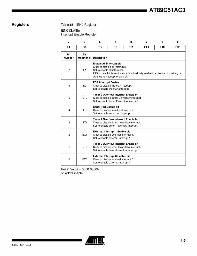
115
AT89C51AC3
4383D–8051–02/08
Registers Table 65. IEN0 Register
IEN0 (S:A8h)
Interrupt Enable Register
Reset Value = 0000 0000b
bit addressable
7 6 5 4 3 2 1 0
EA EC ET2 ES ET1 EX1 ET0 EX0
Bit
Number
Bit
Mnemonic Description
7 EA
Enable All Interrupt bit
Clear to disable all interrupts.
Set to enable all interrupts.
If EA=1, each interrupt source is individually enabled or disabled by setting or
clearing its interrupt enable bit.
6 EC
PCA Interrupt Enable
Clear to disable the PCA interrupt.
Set to enable the PCA interrupt.
5 ET2
Timer 2 Overflow Interrupt Enable bit
Clear to disable Timer 2 overflow interrupt.
Set to enable Timer 2 overflow interrupt.
4 ES
Serial Port Enable bit
Clear to disable serial port interrupt.
Set to enable serial port interrupt.
3 ET1
Timer 1 Overflow Interrupt Enable bit
Clear to disable timer 1 overflow interrupt.
Set to enable timer 1 overflow interrupt.
2 EX1
External Interrupt 1 Enable bit
Clear to disable external interrupt 1.
Set to enable external interrupt 1.
1 ET0
Timer 0 Overflow Interrupt Enable bit
Clear to disable timer 0 overflow interrupt.
Set to enable timer 0 overflow interrupt.
0 EX0
External Interrupt 0 Enable bit
Clear to disable external interrupt 0.
Set to enable external interrupt 0.
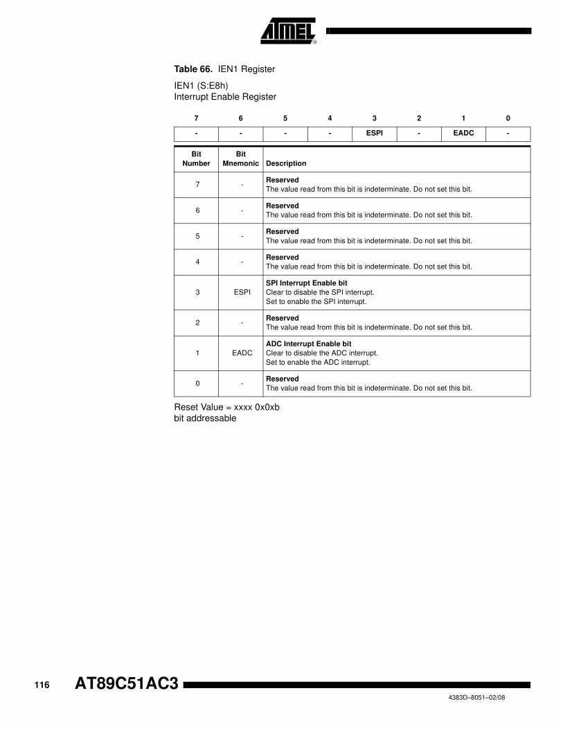
116 AT89C51AC34383D–8051–02/08
Table 66. IEN1 Register
IEN1 (S:E8h)
Interrupt Enable Register
Reset Value = xxxx 0x0xb
bit addressable
7 6 5 4 3 2 1 0
- - - - ESPI - EADC -
Bit
Number
Bit
Mnemonic Description
7 -Reserved
The value read from this bit is indeterminate. Do not set this bit.
6 -Reserved
The value read from this bit is indeterminate. Do not set this bit.
5 -Reserved
The value read from this bit is indeterminate. Do not set this bit.
4 -Reserved
The value read from this bit is indeterminate. Do not set this bit.
3 ESPI
SPI Interrupt Enable bit
Clear to disable the SPI interrupt.
Set to enable the SPI interrupt.
2 -Reserved
The value read from this bit is indeterminate. Do not set this bit.
1 EADC
ADC Interrupt Enable bit
Clear to disable the ADC interrupt.
Set to enable the ADC interrupt.
0 -Reserved
The value read from this bit is indeterminate. Do not set this bit.

117
AT89C51AC3
4383D–8051–02/08
Table 67. IPL0 Register
IPL0 (S:B8h)
Interrupt Enable Register
Reset Value = X000 0000b
bit addressable
7 6 5 4 3 2 1 0
- PPC PT2 PS PT1 PX1 PT0 PX0
Bit
Number
Bit
Mnemonic Description
7 -Reserved
The value read from this bit is indeterminate. Do not set this bit.
6 PPCPCA Interrupt Priority bit
Refer to PPCH for priority level
5 PT2Timer 2 Overflow Interrupt Priority bit
Refer to PT2H for priority level.
4 PSSerial Port Priority bit
Refer to PSH for priority level.
3 PT1Timer 1 Overflow Interrupt Priority bit
Refer to PT1H for priority level.
2 PX1External Interrupt 1 Priority bit
Refer to PX1H for priority level.
1 PT0Timer 0 Overflow Interrupt Priority bit
Refer to PT0H for priority level.
0 PX0External Interrupt 0 Priority bit
Refer to PX0H for priority level.
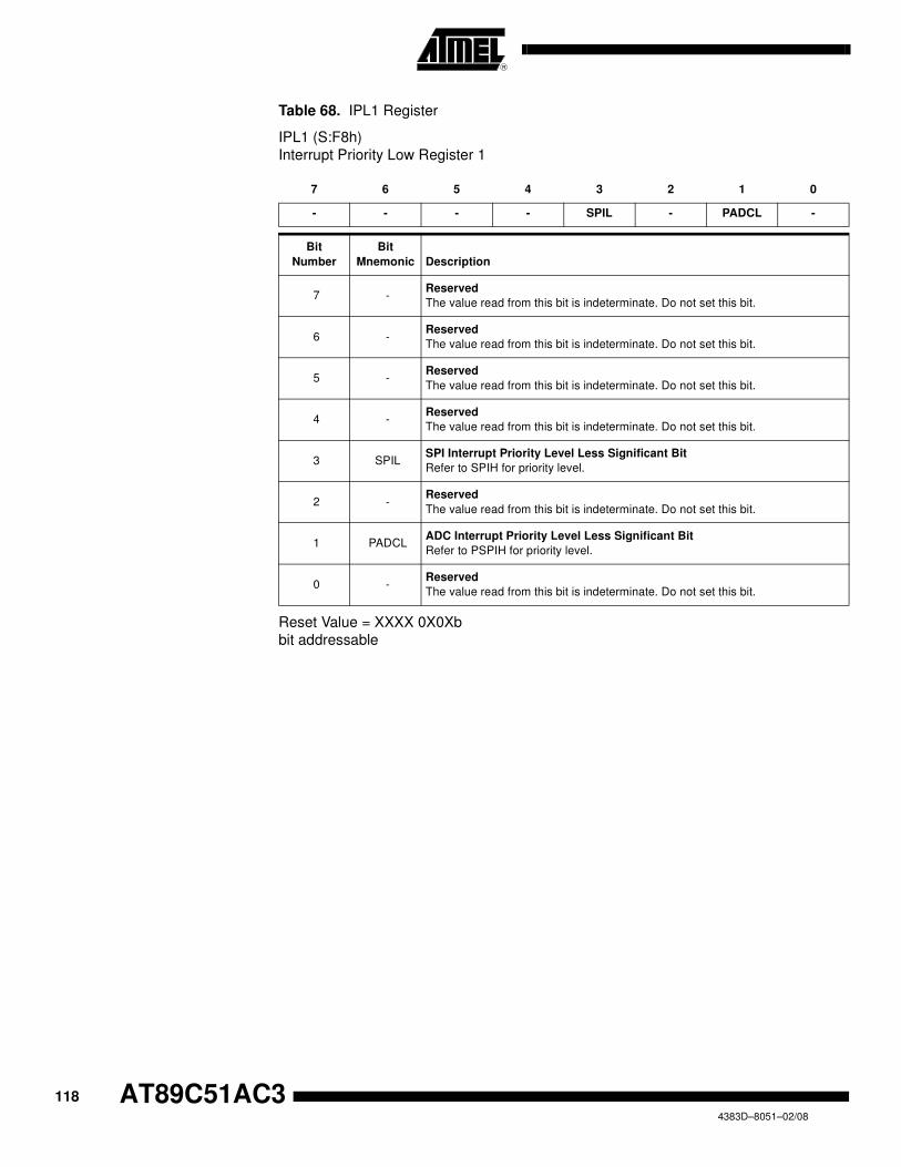
118 AT89C51AC34383D–8051–02/08
Table 68. IPL1 Register
IPL1 (S:F8h)
Interrupt Priority Low Register 1
Reset Value = XXXX 0X0Xb
bit addressable
7 6 5 4 3 2 1 0
- - - - SPIL - PADCL -
Bit
Number
Bit
Mnemonic Description
7 -Reserved
The value read from this bit is indeterminate. Do not set this bit.
6 -Reserved
The value read from this bit is indeterminate. Do not set this bit.
5 -Reserved
The value read from this bit is indeterminate. Do not set this bit.
4 -Reserved
The value read from this bit is indeterminate. Do not set this bit.
3 SPILSPI Interrupt Priority Level Less Significant Bit
Refer to SPIH for priority level.
2 -Reserved
The value read from this bit is indeterminate. Do not set this bit.
1 PADCLADC Interrupt Priority Level Less Significant Bit
Refer to PSPIH for priority level.
0 -Reserved
The value read from this bit is indeterminate. Do not set this bit.

119
AT89C51AC3
4383D–8051–02/08
Table 69. IPL0 Register
IPH0 (B7h)
Interrupt High Priority Register
Reset Value = X000 0000b
7 6 5 4 3 2 1 0
- PPCH PT2H PSH PT1H PX1H PT0H PX0H
Bit
Number
Bit
Mnemonic Description
7 -Reserved
The value read from this bit is indeterminate. Do not set this bit.
6 PPCH
PCA Interrupt Priority Level Most Significant bit
PPCH PPC Priority level
0 0 Lowest
0 1
1 0
1 1 Highest priority
5 PT2H
Timer 2 Overflow Interrupt High Priority bit
PT2H PT2 Priority Level
0 0 Lowest
0 1
1 0
1 1 Highest
4 PSH
Serial Port High Priority bit
PSH PS Priority Level
0 0 Lowest
0 1
1 0
1 1 Highest
3 PT1H
Timer 1 Overflow Interrupt High Priority bit
PT1H PT1 Priority Level
0 0 Lowest
0 1
1 0
1 1 Highest
2 PX1H
External Interrupt 1 High Priority bit
PX1H PX1 Priority Level
0 0 Lowest
0 1
1 0
1 1 Highest
1 PT0H
Timer 0 Overflow Interrupt High Priority bit
PT0H PT0 Priority Level
0 0 Lowest
0 1
1 0
1 1 Highest
0 PX0H
External Interrupt 0 high priority bit
PX0H PX0 Priority Level
0 0 Lowest
0 1
1 0
1 1 Highest
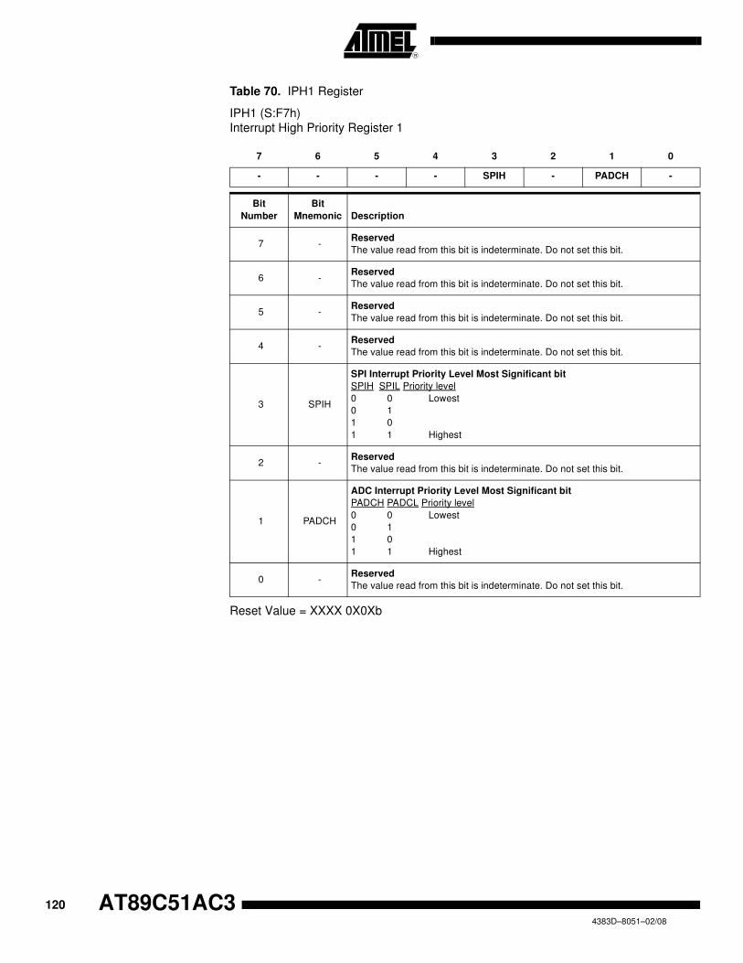
120 AT89C51AC34383D–8051–02/08
Table 70. IPH1 Register
IPH1 (S:F7h)
Interrupt High Priority Register 1
Reset Value = XXXX 0X0Xb
7 6 5 4 3 2 1 0
- - - - SPIH - PADCH -
Bit
Number
Bit
Mnemonic Description
7 -Reserved
The value read from this bit is indeterminate. Do not set this bit.
6 -Reserved
The value read from this bit is indeterminate. Do not set this bit.
5 -Reserved
The value read from this bit is indeterminate. Do not set this bit.
4 -Reserved
The value read from this bit is indeterminate. Do not set this bit.
3 SPIH
SPI Interrupt Priority Level Most Significant bit
SPIH SPIL Priority level
0 0 Lowest
0 1
1 0
1 1 Highest
2 -Reserved
The value read from this bit is indeterminate. Do not set this bit.
1 PADCH
ADC Interrupt Priority Level Most Significant bit
PADCH PADCL Priority level
0 0 Lowest
0 1
1 0
1 1 Highest
0 -Reserved
The value read from this bit is indeterminate. Do not set this bit.

121
AT89C51AC3
4383D–8051–02/08
Electrical Characteristics
Absolute Maximum Ratings
DC Parameters for Standard Voltage
TA = -40°C to +85°C; VSS = 0V;
VCC =2.7V to 5.5V and F = 0 to 40 MHz (both internal and external code execution)
VCC =4.5V to 5.5V and F = 0 to 60 MHz (internal code execution only)
Ambiant Temperature Under Bias:
I = industrial ....................................................... -40°C to 85°C
Storage Temperature .................................... -65°C to + 150°C
Voltage on VCC from VSS ......................................-0.5V to + 6V
Voltage on Any Pin from VSS..................... -0.5V to VCC + 0.2V
Power Dissipation .............................................................. 1 W
Table 71. DC Parameters in Standard Voltage
Symbol Parameter Min Typ(5) Max Unit Test Conditions
VIL Input Low Voltage -0.5 0.2Vcc - 0.1 V
VIH Input High Voltage except XTAL1, RST 0.2 VCC + 0.9 VCC + 0.5 V
VIH1 Input High Voltage, XTAL1, RST 0.7 VCC VCC + 0.5 V
VOL Output Low Voltage, ports 1, 2, 3 and 4(6)
0.3
0.45
1.0
V
V
V
IOL = 100 µA(4)
IOL = 1.6 mA(4)
IOL = 3.5 mA(4)
VOL1 Output Low Voltage, port 0, ALE, PSEN (6)
0.3
0.45
1.0
V
V
V
IOL = 200 µA(4)
IOL = 3.2 mA(4)
IOL = 7.0 mA(4)
VOH Output High Voltage, ports 1, 2, 3, and 4
VCC - 0.3
VCC - 0.7
VCC - 1.5
V
V
V
IOH = -10 µA
IOH = -30 µA
IOH = -60 µA
VCC = 3V to 5.5V
VOH1 Output High Voltage, port 0, ALE, PSEN
VCC - 0.3
VCC - 0.7
VCC - 1.5
V
V
V
IOH = -200 µA
IOH = -3.2 mA
IOH = -7.0 mA
VCC = 5V ± 10%
RRST RST Pulldown Resistor 50 100 200 kΩ
IIL Logical 0 Input Current ports 1, 2, 3 and 4 -50 µA Vin = 0.45V
ILI Input Leakage Current ±10 µA 0.45V < Vin < VCC
ITL
Logical 1 to 0 Transition Current, ports 1, 2, 3
and 4-650 µA Vin = 2.0V
CIO Capacitance of I/O Buffer 10 pFFc = 1 MHz
TA = 25°C
IPD Power-down Current 75 150 µA 3V < VCC < 5.5V(3)
Note: Stresses at or above those listed under “Absolute Maximum
Ratings” may cause permanent damage to the device. This
is a stress rating only and functional operation of the device
at these or any other conditions above those indicated in
the operational sections of this specification is not implied.
Exposure to absolute maximum rating conditions may affect
device reliability.
The power dissipation is based on the maximum allowable
die temperature and the thermal resistance of the package.
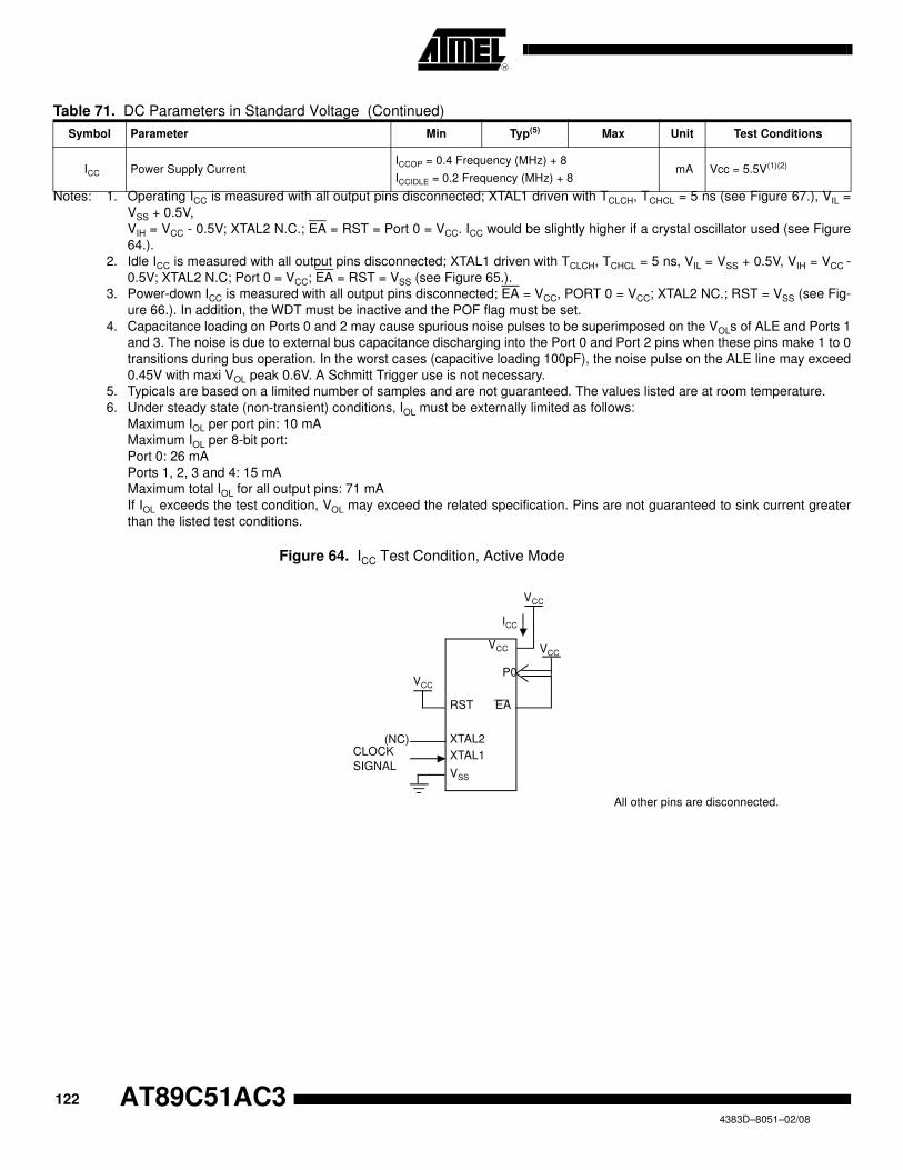
122 AT89C51AC34383D–8051–02/08
Notes: 1. Operating ICC is measured with all output pins disconnected; XTAL1 driven with TCLCH, TCHCL = 5 ns (see Figure 67.), VIL =
VSS + 0.5V,
VIH = VCC - 0.5V; XTAL2 N.C.; EA = RST = Port 0 = VCC. ICC would be slightly higher if a crystal oscillator used (see Figure
64.).
2. Idle ICC is measured with all output pins disconnected; XTAL1 driven with TCLCH, TCHCL = 5 ns, VIL = VSS + 0.5V, VIH = VCC -
0.5V; XTAL2 N.C; Port 0 = VCC; EA = RST = VSS (see Figure 65.).
3. Power-down ICC is measured with all output pins disconnected; EA = VCC, PORT 0 = VCC; XTAL2 NC.; RST = VSS (see Fig-
ure 66.). In addition, the WDT must be inactive and the POF flag must be set.
4. Capacitance loading on Ports 0 and 2 may cause spurious noise pulses to be superimposed on the VOLs of ALE and Ports 1
and 3. The noise is due to external bus capacitance discharging into the Port 0 and Port 2 pins when these pins make 1 to 0
transitions during bus operation. In the worst cases (capacitive loading 100pF), the noise pulse on the ALE line may exceed
0.45V with maxi VOL peak 0.6V. A Schmitt Trigger use is not necessary.
5. Typicals are based on a limited number of samples and are not guaranteed. The values listed are at room temperature.
6. Under steady state (non-transient) conditions, IOL must be externally limited as follows:
Maximum IOL per port pin: 10 mA
Maximum IOL per 8-bit port:
Port 0: 26 mA
Ports 1, 2, 3 and 4: 15 mA
Maximum total IOL for all output pins: 71 mA
If IOL exceeds the test condition, VOL may exceed the related specification. Pins are not guaranteed to sink current greater
than the listed test conditions.
Figure 64. ICC Test Condition, Active Mode
ICC Power Supply CurrentICCOP = 0.4 Frequency (MHz) + 8
ICCIDLE = 0.2 Frequency (MHz) + 8mA Vcc = 5.5V(1)(2)
Table 71. DC Parameters in Standard Voltage (Continued)
Symbol Parameter Min Typ(5) Max Unit Test Conditions
EA
VCC
VCC
ICC
(NC)CLOCK
SIGNAL
VCC
All other pins are disconnected.
RST
XTAL2
XTAL1
VSS
VCC
P0

123
AT89C51AC3
4383D–8051–02/08
Figure 65. ICC Test Condition, Idle Mode
Figure 66. ICC Test Condition, Power-Down Mode
Figure 67. Clock Signal Waveform for ICC Tests in Active and Idle Modes
DC Parameters for A/D Converter
Table 72. DC Parameters for AD Converter in Precision Conversion
Note: 1. Typicals are based on a limited number of samples and are not guaranteed.
RST EA
XTAL2
XTAL1
VSS
VCC
VCC
ICC
(NC)
P0
VCC
All other pins are disconnected.
CLOCK
SIGNAL
RST EA
XTAL2
XTAL1
VSS
VCC
VCC
ICC
(NC)
P0
VCC
All other pins are disconnected.
VCC-0.5V
0.45V
0.7VCC
0.2VCC-0.1
TCLCHTCHCL
TCLCH = TCHCL = 5ns.
Symbol Parameter Min Typ(1) Max Unit Test Conditions
AVin Analog input voltage Vss- 0.2 Vref + 0.2 V
Rref Resistance between Vref and Vss 12 16 24 kΩ
Vref Reference voltage 2.40 3.00 V
Cai Analog input Capacitance 60 pF During sampling
Rai Analog input Resistor 400 Ω During sampling
INL Integral non linearity 1 2 lsb
DNL Differential non linearity 0.5 1 lsb
OE Offset error -2 2 lsb
124 AT89C51AC34383D–8051–02/08
AC Parameters
Explanation of the AC
Symbols
Each timing symbol has 5 characters. The first character is always a “T” (stands for
time). The other characters, depending on their positions, stand for the name of a signal
or the logical status of that signal. The following is a list of all the characters and what
they stand for.
Example: TAVLL = Time for Address Valid to ALE Low.
TLLPL = Time for ALE Low to PSEN Low.
TA = -40°C to +85°C; VSS = 0V; VCC = 3V to 5.5V; F = 0 to 40 MHz.
(Load Capacitance for port 0, ALE and PSEN = 60 pF; Load Capacitance for all other
outputs = 60 pF.)
Table 73, Table 76 and Table 79 give the description of each AC symbols.
Table 74, Table 78 and Table 80 give for each range the AC parameter.
Table 75, Table 78 and Table 81 give the frequency derating formula of the AC parame-
ter for each speed range description. To calculate each AC symbols: Take the x value
and use this value in the formula.
Example: TLLIV and 20 MHz, Standard clock.
x = 30 ns
T = 50 ns
TCCIV = 4T - x = 170 ns

125
AT89C51AC3
4383D–8051–02/08
External Program Memory
Characteristics
Table 73. Symbol Description
Table 74. AC Parameters for a Fix Clock (F = 40 MHz)
Symbol Parameter
T Oscillator clock period
TLHLL ALE pulse width
TAVLL Address Valid to ALE
TLLAX Address Hold After ALE
TLLIV ALE to Valid Instruction In
TLLPL ALE to PSEN
TPLPH PSEN Pulse Width
TPLIV PSEN to Valid Instruction In
TPXIX Input Instruction Hold After PSEN
TPXIZ Input Instruction Float After PSEN
TAVIV Address to Valid Instruction In
TPLAZ PSEN Low to Address Float
Symbol Min Max Units
T 25 ns
TLHLL 40 ns
TAVLL 10 ns
TLLAX 10 ns
TLLIV 70 ns
TLLPL 15 ns
TPLPH 55 ns
TPLIV 35 ns
TPXIX 0 ns
TPXIZ 18 ns
TAVIV 85 ns
TPLAZ 10 ns
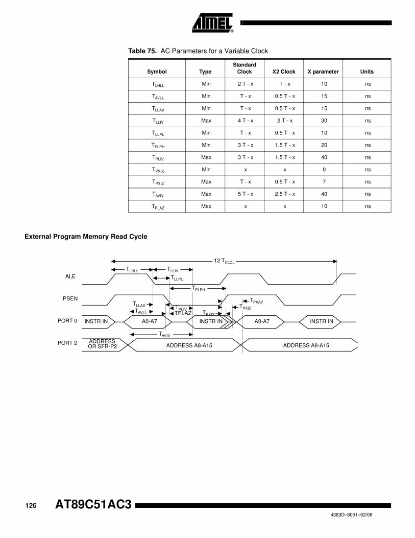
126 AT89C51AC34383D–8051–02/08
Table 75. AC Parameters for a Variable Clock
External Program Memory Read Cycle
Symbol Type
Standard
Clock X2 Clock X parameter Units
TLHLL Min 2 T - x T - x 10 ns
TAVLL Min T - x 0.5 T - x 15 ns
TLLAX Min T - x 0.5 T - x 15 ns
TLLIV Max 4 T - x 2 T - x 30 ns
TLLPL Min T - x 0.5 T - x 10 ns
TPLPH Min 3 T - x 1.5 T - x 20 ns
TPLIV Max 3 T - x 1.5 T - x 40 ns
TPXIX Min x x 0 ns
TPXIZ Max T - x 0.5 T - x 7 ns
TAVIV Max 5 T - x 2.5 T - x 40 ns
TPLAZ Max x x 10 ns
TPLIVTPLAZ
ALE
PSEN
PORT 0
PORT 2
A0-A7A0-A7 INSTR ININSTR IN INSTR IN
ADDRESSOR SFR-P2 ADDRESS A8-A15ADDRESS A8-A15
12 TCLCL
TAVIV
TLHLL
TAVLL
TLLIV
TLLPL
TPLPH
TPXAV
TPXIX
TPXIZTLLAX

127
AT89C51AC3
4383D–8051–02/08
External Data Memory
Characteristics
Table 76. Symbol Description
Table 77. AC Parameters for a Variable Clock (F=40MHz)
Symbol Parameter
TRLRH RD Pulse Width
TWLWH WR Pulse Width
TRLDV RD to Valid Data In
TRHDX Data Hold After RD
TRHDZ Data Float After RD
TLLDV ALE to Valid Data In
TAVDV Address to Valid Data In
TLLWL ALE to WR or RD
TAVWL Address to WR or RD
TQVWX Data Valid to WR Transition
TQVWH Data set-up to WR High
TWHQX Data Hold After WR
TRLAZ RD Low to Address Float
TWHLH RD or WR High to ALE high
Symbol Min Max Units
TRLRH 130 ns
TWLWH 130 ns
TRLDV 100 ns
TRHDX 0 ns
TRHDZ 30 ns
TLLDV 160 ns
TAVDV 165 ns
TLLWL 50 100 ns
TAVWL 75 ns
TQVWX 10 ns
TQVWH 160 ns
TWHQX 15 ns
TRLAZ 0 ns
TWHLH 10 40 ns

128 AT89C51AC34383D–8051–02/08
Table 78. AC Parameters for a Variable Clock
Symbol Type
Standard
Clock X2 Clock X parameter Units
TRLRH Min 6 T - x 3 T - x 20 ns
TWLWH Min 6 T - x 3 T - x 20 ns
TRLDV Max 5 T - x 2.5 T - x 25 ns
TRHDX Min x x 0 ns
TRHDZ Max 2 T - x T - x 20 ns
TLLDV Max 8 T - x 4T -x 40 ns
TAVDV Max 9 T - x 4.5 T - x 60 ns
TLLWL Min 3 T - x 1.5 T - x 25 ns
TLLWL Max 3 T + x 1.5 T + x 25 ns
TAVWL Min 4 T - x 2 T - x 25 ns
TQVWX Min T - x 0.5 T - x 15 ns
TQVWH Min 7 T - x 3.5 T - x 25 ns
TWHQX Min T - x 0.5 T - x 10 ns
TRLAZ Max x x 0 ns
TWHLH Min T - x 0.5 T - x 15 ns
TWHLH Max T + x 0.5 T + x 15 ns

129
AT89C51AC3
4383D–8051–02/08
External Data Memory Write Cycle
External Data Memory Read Cycle
Serial Port Timing – Shift Register Mode
Table 79. Symbol Description (F = 40 MHz)
TQVWHTLLAX
ALE
PSEN
WR
PORT 0
PORT 2
A0-A7 DATA OUT
ADDRESSOR SFR-P2
TAVWL
TLLWL
TQVWX
ADDRESS A8-A15 OR SFR P2
TWHQX
TWHLH
TWLWH
ALE
PSEN
RD
PORT 0
PORT 2
A0-A7 DATA IN
ADDRESSOR SFR-P2
TAVWL
TLLWL
TRLAZ
ADDRESS A8-A15 OR SFR P2
TRHDZ
TWHLH
TRLRH
TLLDV
TRHDXTLLAX
TAVDV
Symbol Parameter
TXLXL Serial port clock cycle time
TQVHX Output data set-up to clock rising edge
TXHQX Output data hold after clock rising edge
TXHDX Input data hold after clock rising edge
TXHDV Clock rising edge to input data valid
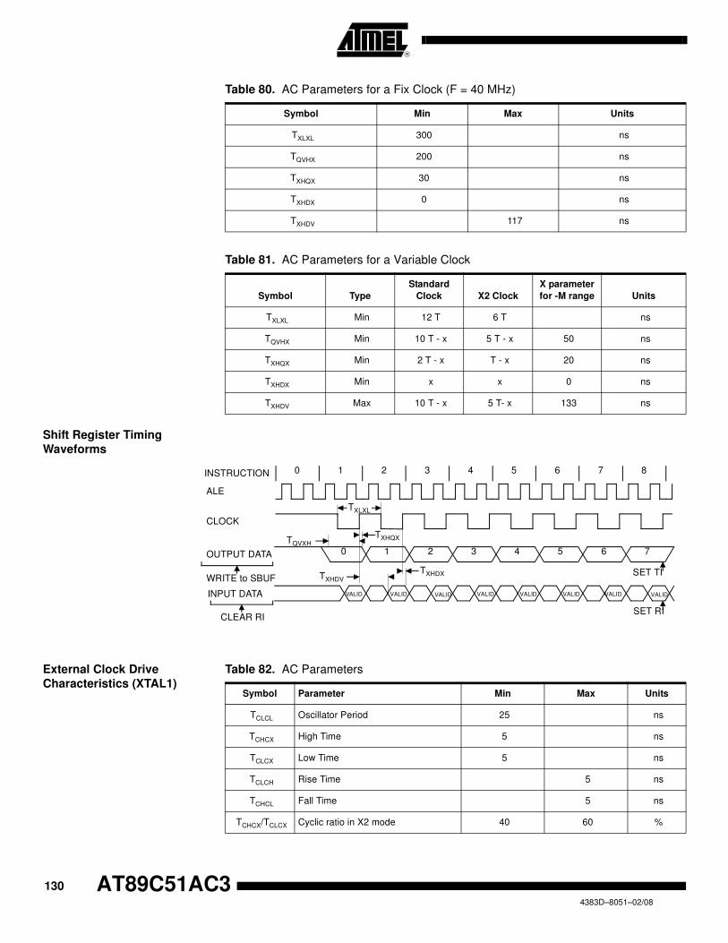
130 AT89C51AC34383D–8051–02/08
Table 80. AC Parameters for a Fix Clock (F = 40 MHz)
Table 81. AC Parameters for a Variable Clock
Shift Register Timing
Waveforms
External Clock Drive
Characteristics (XTAL1)
Table 82. AC Parameters
Symbol Min Max Units
TXLXL 300 ns
TQVHX 200 ns
TXHQX 30 ns
TXHDX 0 ns
TXHDV 117 ns
Symbol Type
Standard
Clock X2 Clock
X parameter
for -M range Units
TXLXL Min 12 T 6 T ns
TQVHX Min 10 T - x 5 T - x 50 ns
TXHQX Min 2 T - x T - x 20 ns
TXHDX Min x x 0 ns
TXHDV Max 10 T - x 5 T- x 133 ns
VALID VALID VALID VALID VALIDVALIDINPUT DATA VALID
0 1 2 3 4 5 6 87
ALE
CLOCK
OUTPUT DATA
WRITE to SBUF
CLEAR RI
TXLXL
TQVXHTXHQX
TXHDV
TXHDX SET TI
SET RI
INSTRUCTION
0 1 2 3 4 5 6 7
VALID
Symbol Parameter Min Max Units
TCLCL Oscillator Period 25 ns
TCHCX High Time 5 ns
TCLCX Low Time 5 ns
TCLCH Rise Time 5 ns
TCHCL Fall Time 5 ns
TCHCX/TCLCX Cyclic ratio in X2 mode 40 60 %

131
AT89C51AC3
4383D–8051–02/08
External Clock Drive
Waveforms
AC Testing Input/Output
Waveforms
AC inputs during testing are driven at VCC - 0.5 for a logic “1” and 0.45V for a logic “0”.
Timing measurement are made at VIH min for a logic “1” and VIL max for a logic “0”.
Float Waveforms
For timing purposes as port pin is no longer floating when a 100 mV change from load
voltage occurs and begins to float when a 100 mV change from the loaded VOH/VOL level
occurs. IOL/IOH ≥ ± 20 mA.
VCC-0.5V
0.45V
0.7VCC
0.2VCC-0.1
TCHCL TCLCX
TCLCL
TCLCH
TCHCX
INPUT/OUTPUT0.2 VCC + 0.9
0.2 VCC - 0.1
VCC -0.5V
0.45V
FLOAT
VOH - 0.1 V
VOL + 0.1 V
VLOADVLOAD + 0.1 V
VLOAD - 0.1 V

132 AT89C51AC34383D–8051–02/08
Clock Waveforms Valid in normal clock mode. In X2 mode XTAL2 must be changed to XTAL2/2.
This diagram indicates when signals are clocked internally. The time it takes the signals to propagate to the pins, however,
ranges from 25 to 125 ns. This propagation delay is dependent on variables such as temperature and pin loading. Propaga-
tion also varies from output to output and component. Typically though (TA=25°C fully loaded) RD and WR propagation
delays are approximately 50ns. The other signals are typically 85 ns. Propagation delays are incorporated in the AC
specifications.
DATA PCL OUT DATA PCL OUT DATA PCL OUT SAMPLED SAMPLED SAMPLED
STATE4 STATE5 STATE6 STATE1 STATE2 STATE3 STATE4 STATE5
P1 P2 P1 P2 P1 P2 P1 P2 P1 P2 P1 P2 P1 P2 P1 P2
FLOAT FLOAT FLOAT
THESE SIGNALS ARE NOT ACTIVATED DURING THEEXECUTION OF A MOVX INSTRUCTION
INDICATES ADDRESS TRANSITIONS
EXTERNAL PROGRAM MEMORY FETCH
FLOAT
DATASAMPLED
DPL OR Rt OUT
INDICATES DPH OR P2 SFR TO PCH TRANSITION
PCL OUT (IF PROGRAMMEMORY IS EXTERNAL)
PCL OUT (EVEN IF PROGRAMMEMORY IS INTERNAL)
PCL OUT (IF PROGRAMMEMORY IS EXTERNAL)
OLD DATA NEW DATA
P0 PINS SAMPLED
P1, P2, P3 PINS SAMPLED P1, P2, P3 PINS SAMPLED
P0 PINS SAMPLED
RXD SAMPLED
INTERNALCLOCK
XTAL2
ALE
PSEN
P0
P2 (EXT)
READ CYCLE
WRITE CYCLE
RD
P0
P2
WR
PORT OPERATION
MOV PORT SRC
MOV DEST P0
MOV DEST PORT (P1. P2. P3)(INCLUDES INTO. INT1. TO T1)
SERIAL PORT SHIFT CLOCK
TXD (MODE 0)
DATA OUT
DPL OR Rt OUT
INDICATES DPH OR P2 SFR TO PCH TRANSITION
P0
P2
RXD SAMPLED

133
AT89C51AC3
4383D–8051–02/08
Flash/EEPROM Memory Table 83. Timing Symbol Definitions
Table 84. Memory AC Timing
VDD = 3V to 5.5V, TA = -40 to +85°C
Figure 68. Flash Memory – ISP Waveforms
Figure 69. Flash Memory – Internal Busy Waveforms
Signals Conditions
S (Hardware
condition)PSEN#,EA L Low
R RST V Valid
B FBUSY flag X No Longer Valid
Symbol Parameter Min Typ Max Unit
TSVRL Input PSEN# Valid to RST Edge 50 ns
TRLSX Input PSEN# Hold after RST Edge 50 ns
TBHBL
Flash/EEPROM Internal Busy
(Programming) Time10 ms
RST
TSVRL
PSEN#1
TRLSX
FBUSY bitTBHBL

134 AT89C51AC34383D–8051–02/08
Ordering InformationTable 85. Possible Order Entries
Part Number Boot Loader Temperature Range Package Packing Product Marking
AT89C51AC3-RLTIM
OBSOLETEAT89C51AC3-SLSIM
AT89C51AC3-RDTIM
AT89C51AC3-S3SIM
AT89C51AC3-RLTUM UART Industrial & Green VQFP44 Tray AT89C51AC3-M
AT89C51AC3-SLSUM UART Industrial & Green PLCC44 Stick AT89C51AC3-IM
AT89C51AC3-RDTUM UART Industrial & Green VQFP64 Tray AT89C51AC3-IM
AT89C51AC3-S3SUM UART Industrial & Green PLCC52 Stick AT89C51AC3-IM

135
AT89C51AC3
4383D–8051–02/08
Package Drawing
VQFP44
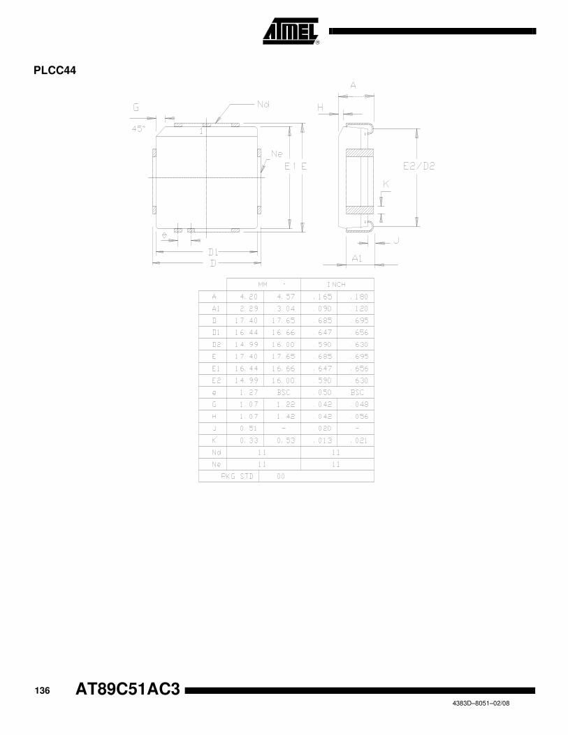
136 AT89C51AC34383D–8051–02/08
PLCC44
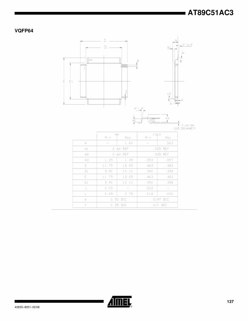
137
AT89C51AC3
4383D–8051–02/08
VQFP64

138 AT89C51AC34383D–8051–02/08
PLCC52

139
AT89C51AC3
4383D–8051–02/08
Document Revision History
Changes from 4383A 10/04 - 4383B 01/05
1. Various minor corrections made throughout the document.
2. Clarification to Mode Switching Waveforms diagram. See page 17.
Changes from 4383B 01/05 to 4383C 11/05
1. Added Green product ordering information.
Changes from 4383C 11/05 to 4383D 02/08
1. Removed non green products from ordering information.

Printed on recycled paper.
© Atmel Corporation 2008.Atmel Corporation makes no warranty for the use of its products, other than those expressly contained in the Company’s standard warrantywhich is detailed in Atmel’s Terms and Conditions located on the Company’s web site. The Company assumes no responsibility for any errorswhich may appear in this document, reserves the right to change devices or specifications detailed herein at any time without notice, and doesnot make any commitment to update the information contained herein. No licenses to patents or other intellectual property of Atmel are grantedby the Company in connection with the sale of Atmel products, expressly or by implication. Atmel’s products are not authorized for use as criticalcomponents in life support devices or systems.
Atmel Headquarters Atmel Operations
Corporate Headquarters2325 Orchard ParkwaySan Jose, CA 95131TEL 1(408) 441-0311FAX 1(408) 487-2600
EuropeAtmel SarLRoute des Arsenaux 41Casa Postale 80CH-1705 FribourgSwitzerlandTEL (41) 26-426-5555FAX (41) 26-426-5500
AsiaAtmel Asia, Ltd.Room 1219Chinachem Golden Plaza77 Mody Road TsimhatsuiEast KowloonHong KongTEL (852) 2721-9778FAX (852) 2722-1369
JapanAtmel Japan K.K.9F, Tonetsu Shinkawa Bldg.1-24-8 ShinkawaChuo-ku, Tokyo 104-0033JapanTEL (81) 3-3523-3551FAX (81) 3-3523-7581
MemoryAtmel Corporate2325 Orchard ParkwaySan Jose, CA 95131TEL 1(408) 436-4270FAX 1(408) 436-4314
MicrocontrollersAtmel Corporate2325 Orchard ParkwaySan Jose, CA 95131TEL 1(408) 436-4270FAX 1(408) 436-4314
Atmel NantesLa ChantrerieBP 7060244306 Nantes Cedex 3, FranceTEL (33) 2-40-18-18-18FAX (33) 2-40-18-19-60
ASIC/ASSP/Smart CardsAtmel RoussetZone Industrielle13106 Rousset Cedex, FranceTEL (33) 4-42-53-60-00FAX (33) 4-42-53-60-01
Atmel Colorado Springs1150 East Cheyenne Mtn. Blvd.Colorado Springs, CO 80906TEL 1(719) 576-3300FAX 1(719) 540-1759
Atmel Smart Card ICsScottish Enterprise Technology ParkMaxwell BuildingEast Kilbride G75 0QR, Scotland TEL (44) 1355-803-000FAX (44) 1355-242-743
RF/AutomotiveAtmel HeilbronnTheresienstrasse 2Postfach 353574025 Heilbronn, GermanyTEL (49) 71-31-67-0FAX (49) 71-31-67-2340
Atmel Colorado Springs1150 East Cheyenne Mtn. Blvd.Colorado Springs, CO 80906TEL 1(719) 576-3300FAX 1(719) 540-1759
Biometrics/Imaging/Hi-Rel MPU/High Speed Converters/RF Data-com
Atmel GrenobleAvenue de RochepleineBP 12338521 Saint-Egreve Cedex, FranceTEL (33) 4-76-58-30-00FAX (33) 4-76-58-34-80
Web Sitehttp://www.atmel.com
4383D–8051–02/08 /xM