Embed Size (px)
Citation preview

arX
iv:1
705.
1042
9v1
[co
nd-m
at.m
es-h
all]
30
May
201
7
Engineering of Neutral Excitons and Exciton
Complexes in Transition Metal Dichalcogenide
Monolayers through External Dielectric Screening
Sven Borghardt1, Jhih-Sian Tu1, Florian Winkler2,3, Jurgen
Schubert1, Willi Zander1, Kristjan Lesson4, Beata E.
Kardyna l1
1 Peter Grunberg Institute 9 (PGI-9), Forschungszentrum Julich, DE-52425
Julich, Germany
2 Ernst Ruska-Centre for Microscopy and Spectroscopy with Electrons (ER-C),
Forschungszentrum Julich, DE-52425 Julich, Germany
3 Peter Grunberg Institute 5 (PGI-5), Forschungszentrum Julich, DE-52425
Julich, Germany
4 Innovation Center Iceland, Keldnaholti, IS-112 Reykjavik, Iceland
E-mail: [email protected]
May 2017
Abstract. In order to fully exploit the potential of transition metal
dichalcogenide monolayers (TMD-MLs), the well-controlled creation of atomically
sharp lateral heterojunctions within these materials is highly desirable. A
promising approach to create such heterojunctions is the local modulation of the
electronic structure of an intrinsic TMD-ML via dielectric screening induced by
its surrounding materials. For the realization of this non-invasive approach, an
in-depth understanding of such dielectric effects is required. We report on the
modulations of excitonic transitions in TMD-MLs through the effect of dielectric
environments including low-k and high-k dielectric materials. We present absolute
tuning ranges as large as 37 meV for the optical band gaps of WSe2 and MoSe2 MLs
and relative tuning ranges on the order of 30% for the binding energies of neutral
excitons in WSe2 MLs. The findings suggest the possibility to reduce the electronic
band gap of WSe2 MLs by 120 meV, paving the way towards dielectrically defined
lateral heterojunctions.

2
Keywords: Transition Metal Dichalcogenides, Tungsten Diselenide, Molybdenum
Diselenide, Exciton, Trion, Photoluminescence, Reflectance, Dielectric Screening,
Lateral Heterojunction, Two-Dimensional Material

3
1. Introduction
Since the discovery of graphene the class
of atomically thin two-dimensional materials
has been growing continuously [1–4]. An
exciting expansion of this class was done when
transition metal dichalcogenide monolayers
(TMD-MLs) were added to this material class
[5]. In contrast to the semimetal graphene,
TMD-MLs with the stoichiometric formula
MX2, where M and X denote a transition metal
atom (Mo, W, ...) and a chalcogen atom
(S, Se, ...), respectively, are semiconductors
with direct band gaps at the K-points of
the hexagonal Brillouin zone with energies in
the range of visible light [6]. Additionally,
the heavy metal ions, the reduced Coulomb
screening in two dimensions and the lack of
inversion symmetry in these materials result in
a unique combination of giant exciton binding
energies, large spin-orbit coupling, as well as a
coupling between the spin and valley degrees
of freedom at the two inequivalent K-valleys
that can be accessed optically [7–9].
Although there have been numerous re-
ports on electronic and optoelectronic nanode-
vices made from TMD-MLs such as single-layer
transistors, light-emitting diodes and photode-
tectors [10–12], there is a strong need to de-
velop methods to create junctions. In analogy
to well established semiconductor technology,
where heterojunctions are the building blocks
of most electronic and optoelectronic devices
(e.g. laser diodes, HEMT transistors), the re-
liable creation of lateral heterojunctions within
TMD-MLs would enable further development
of next generation optoelectronic devices.
In analogy to three dimensional semi-
conductors where heterostructures are formed
by interfacing materials of different chemical
composition, lateral heterostructures of TMDs
have been developed by introducing laterally
Figure 1. Schematic diagram of externally induced
dielectric screening effects on the electronic and optical
band gaps at the K-point of TMD-MLs. Solid
arrows, dashed arrows and waved arrows represent
optical absorption processes, non-radiative relaxation
processes and radiative recombination processes,
respectively.
varying stoichiometry [13, 14]. An alterna-
tive approach, which is unique to low dimen-
sional materials, relies on the local modulation
of screening of the ionic Coulomb potentials,
as well as the Coulomb interaction between
charge carriers, within the ML [15,16] through
a local variation of the relative permittivity of
the ML’s direct environment, i.e. its substrate
and cover material.
Fig. 1 depicts how externally induced
screening changes both the electronic and
optical band gaps of a TMD-ML. Both the
electronic band gap, Eg, and the binding
energy of the neutral exciton, Eb, in the
monolayer are expected to decrease with
an increasing relative permittivity of the
surrounding dielectric [15–18]. The sign of
the change of the optical band gap, Ex =
Eg−Eb, depends on the relative change of these
two quantities and can be probed optically
by measuring the energy of free, neutral
excitons. In addition to neutral excitons,
charged exciton states (trions) with binding
energies, ET± = Ex − Ex±, on the order

4
Figure 2. Symbolic diagram of the structures
studied in this work, together with the average relative
permittivity of the substrate and cover material in each
structure.
of 30 meV have been observed in TMD-MLs
[19–22]. Similarly to the binding energies
of neutral excitons, the binding energies of
trions in ML’s are expected to decrease with
an increasing background relative permittivity
[18]. Negatively charged trions are expected to
be present in unbiased TMD-MLs, which are
known to be unintentionally n-doped [19–22].
A first experimental evidence for the
tunability of excitonic properties in TMD-
MLs through environment-induced dielectric
screening has been the report of a room
temperature blue shift of Ex and Ex− in MoS2
MLs with an increasing relative permittivity
of the non-ionic liquid with which the samples
were covered [23]. More recently, an increase of
the exciton Bohr radius in WSe2 MLs with an
increasing background relative permittivity of
the surrounding material of the ML has been
observed [24]. In addition, a decrease of the
exciton binding energy and the electronic band
gap has been observed for WS2 MLs stacked
with graphene [25].
In this work, we investigate different
types of dielectrics as potential components
of lateral heterostructure. We employ low
temperature µ-photoluminescence, as well as
reflectance measurements to study MoSe2
and WSe2 MLs. Our results show a red-
shift of the optical band gaps, as well as
a reduction of the binding energies of both
the neutral exciton and the trion, with an
increasing average relative permittivity of the
ML’s surrounding. Estimates on the resulting
changes of the electronic band gaps are made
from the measured optical band gaps and
exciton binding energies.
2. Experiments
Mechanically exfoliated WSe2 and MoSe2 MLs
have been prepared on different substrates.
The substrates were required to be flat in
order to minimize the strain and the number
of defects introduced in the TMD-MLs. Only
transparent wide band gap materials were
used. The subsrates considered in this work
can be separated into three types (fig. 2 a)-
c)) according to their surface properties. The
first type of substrate, namely CYTOP, is
a low-k fluoropolymer, which is known for
its chemical inertness and hydrophobicity. It
is amorphous and transparent across a wide
wavelength range and it features a very low
relative permittivity for the entire frequency
range. The second type are stable, transparent
oxide substrates. Oxides offer a wide range of
k-values but they are known to be hydrophilic.
Hexagonal boron-nitride (h-BN) is a wide
band gap layered material that can form van-
der-Waals heterostructures with TMD-MLs.
Similarly to CYTOP, h-BN is hydrophobic.
A TMD-ML encapsulated by two hexagonal
h-BN flakes was also included as a fourth
dielectric environment (fig. 2 d)).
On a theoretical level, the effect of
dielectric screening on excitonic properties is
complex and non-analytic. Especially, an open
question remains in which frequency domains
the screening occurs. In our analysis, for the

5
sake of simplicity, we identify the surrounding
materials by their static dielectric constant.
This represents a simplification, however,
we emphasize that it does not change the
conclusions from this work. A more detailed
discussion of this point can be found in the
Supporting Information. The average nominal
relative permittivity of the environment, ǫav. =1
2(ǫtop + ǫbottom), ranged from 1.5 for a TMD-
ML on CYTOP to 12.4 for a TMD-ML on
LaAlO3. All the layers in contact with the MLs
were at least several nanometers thick and, as
a consequence, only the layers in direct contact
with the TMD-ML are needed to be included
in the analysis.
µ-photoluminescence maps, as well as op-
tical reflectance measurements of all struc-
tures were acquired at 11 K. While the former
method only probes the emission energies of
the ground states of neutral excitons and tri-
ons, absorption energies of the ground state, as
well as of excited states, of the neutral exciton
can be probed by the latter [26,27]. We further
analyze the impact of charging induced by the
substrate or the cover material as the reason
for the observed effects.
3. Results
The emission energies of the neutral exciton
and the trion of all structures shown in figure
2 have been measured in µ-photoluminescence
experiments. Figure 3 shows photolumines-
cence spectra for three representative struc-
tures. The spectra contain signal from neu-
tral exciton and trion recombination, as well
as defect emission in the case of WSe2 MLs.
The energy of these peaks shows a system-
atic shift with ǫav.. Figure 4, summarizes the
emission energies for both the neutral exciton
and the trion for all measured structures. The
data points are averaged over large areas in
1.6 1.7
energy [eV]
1.6 1.7 1.8
energy [eV]
photoluminescence
[a.u.]
vacuumCYTOP
ǫ=
1.5
vacuumh-BN
ǫ=
3.9
h-BNh-BN ǫ
=6.9
vacuumCYTOP
ǫ=
1.5
vacuumh-BN
ǫ=
3.9
h-BNh-BN
ǫ=
6.9
a) WSe2 b) MoSe2
Figure 3. Representative photoluminescence spectra
for WSe2 (a) and MoSe2 (b) MLs in different dielectric
environments. The highest and second highest energy
peak in each spectrum represent the neutral exciton
and trion emission, respectively. For WSe2, a band of
defects can be observed at the low energy end of the
spectra. The dotted black lines connect the neutral
exciton and trion emission peaks of each spectrum, as
a guidance to the eye.
order to account for spatial variations of the
peak positions. The trends in behaviour of
WSe2 and MoSe2 MLs in different environ-
ments are very similar. The results for both
TMD-MLs on SiO2, which is the most com-
monly used substrate, agree well with reports
in the literature [19, 28]. There is a clear
correlation in the positions of neutral exciton
and trion peaks but there is no clear corre-
lation with the nominal ǫav.. Irrespective of
the nominal relative permittivity of the sub-
strate, the emission energies for MLs on CY-
TOP and for MLs on oxide substrates are
very similar to each other and cluster around
(Ex, Ex−) = (1.754eV, 1.717eV) for WSe2 and
at (Ex, Ex−) = (1.664eV, 1.631eV) for MoSe2.
We attribute this effect to the presence of wa-
ter on the hydrophilic oxide surface preventing
a direct contact between the substrate material
and the TMD-MLs. Hexagonal ice has a rela-
tive permittivity below 2 [29] and, thus, similar

6
Figure 4. Emission energies of the neutral exciton and the trion in WSe2 (a) and MoSe2 (b) MLs for different
dielectric environments. The legend shows the substrate and the cover material below and above the horizontal
line, respectively. The color of the plotted data represents ǫav.. The emission energies at each sample position
have been obtained by hyperspectral fitting using a purpose-developed software (see Supporting Information)
and the mean values and error bars are obtained by a pixel-by-pixel averaging over the sample area.
to that of CYTOP.
Even though the relative permittivity of
h-BN is lower than that of some oxides,
the emission energies of MLs on a h-BN
substrate, as well as of MLs encapsulated
in h-BN, show clearly observable red-shifts
with respect to this cluster. For the neutral
exciton, the red-shifts with respect to a ML on
CYTOP are 17 meV (16 meV) and 35 meV
(34 meV) for WSe2 (MoSe2) MLs on h-BN
and encapsulated with h-BN, respectively. For
the trion, the red-shifts with respect to a
ML on CYTOP are 14 meV (16 meV) and
29 meV (31 meV) for WSe2 (MoSe2) MLs on h-
BN and encapsulated with h-BN, respectively.
It is well known that contamination is
highly mobile in mechanically stacked van-
der-Waals heterostructures clustering into so-
called bubbles leaving behind large areas of
clean interfaces (Supporting Info, fig. 1)
[30]. Since this contamination covers only
a very small fraction of the sample area,
the photoluminescence emission from the
clean interfaces is expected to dominate the
measured signal.
The observed red-shifts for the h-BN
structures imply that the electronic band gap
is undergoing a larger absolute change than the
exciton binding energies when increasing ǫav..
These findings are in contrast to previously
reported observations in room temperature
measurements of MoS2 MLs in dielectric non-
ionic liquids [23], but agree well with recent
reflectance studies of TMD-MLs stacked with
graphene [25].
Figure 5 shows the evolution of the trion
binding energy, determined from the difference
between neutral exciton and trion energies,

7
2 4 6 826
28
30
32
34
36
ǫav.
Ex−E
x−[m
eV]
vacuum
CYTOP
vacuum
h-B
N
h-B
Nh-B
N
MoSe2
WSe2
Figure 5. Trion binding energies in WSe2 and
MoSe2 monolayers, as a function of ǫav.. The binding
energies at each sample position have been obtained
by hyperspectral fitting using a purpose-developed
software (see Supporting Information) and the mean
values and error bars are obtained by a pixel-by-pixel
averaging over the sample area.
as a function of ǫav., for MoSe2 and WSe2.
For WSe2 the trion binding energy decreases
monotonically from 35 meV for a ML on
CYTOP to 29 meV for a ML encapsulated
in h-BN. This result is in good qualitative
agreement with theoretical predictions [18]. In
contrast, the trion binding energy of a MoSe2ML is nearly identical for a ML on CYTOP
and a ML on h-BN. However, similarly to
WSe2, the trion binding energy of MoSe2decreases from 30 meV for a ML on h-BN
to 27 meV for a ML encapsulated between
two h-BN flakes. The small change between
the trion binding energy of a MoSe2 ML on
CYTOP and a MoSe2 ML on h-BN is still
under investigation. A possible explanation
may be a positive polarity of the trion for a
ML on CYTOP, which, having a lower binding
energy than negatively charged trions would
cancel out the effect of the reduced screening
[28]. An indication for a different background
charge for the ML on CYTOP is the different
exciton-trion ratio observed in this structure
(fig. 3). The trion binding energies are
determined as the average difference between
the exciton and trion emission energies and
the standard deviations shown in figure
5 are up to five times lower than those
determined for the exciton and trion emission
energies themselves (fig. 4). This lower
spatial fluctuation of the trion binding energy,
indicates the robustness of excitonic binding
energies against perturbations such as strain,
as expected from theoretical studies [31]. Trion
binding energies could thus be potentially
used as a sensitive probe of surface state
of transition metal dichalcogenide monolayers,
providing a non-invasive alternative to the use
of water droplets [32].
Changes of the optical band gap of TMD-
MLs with spatially modulated ǫav. are shown
in figure 6 for a single MoSe2 ML. The sample
is prepared by placing the ML on an interface
between SiO2 and hBN and partially covering
it with a hBN layer. While small variations
of Ex within a region of constant ǫav. are
present, the correlation of Ex with the local
ǫav. of the TMD-ML is clear. The residual
variations within each region are most likely
due to strain variations, which are known to
change the ML’s electronic band gap [33]. A
line profile across the boundary, that separates
the part of the monolayer encapsulated in h-
BN from the uncovered part on h-BN is shown
in figure 6 c). In the line profile, it can be
seen that the change of the optical band gap
is observed over a distance of approximately
1.5 µm, which is the size of the laser spot in
our measurements. Consequently, the band
gap change is much more abrupt than the
radius of the laser spot, which agrees well
with theoretical predictions of the transition

8
Figure 6. MoSe2 monolayer in different dielectric environments. a) Optical micrograph of the TMD-ML (yellow
line), which is partly lying on a SiO2 substrate and partly lying on a h-BN flake (blue line). Furthermore, a
part of the latter sample area is covered with another h-BN flake (magenta line). The scale bar is 20 µm. b)
Spatial distribution of the exciton emission energy of the TMD-ML. Note that some pixels needed to be removed
from the analysis when they showed disturbed photoluminescence spectra or when they probed two dielectric
environments at the same time. c) Normalized intensities for the neutral exciton emission from the ML on h-BN
and the ML encapsulated by h-BN along the a path marked by the red arrow in b). d) Representative spectra
along the same path.
occuring across only a few crystal unit cells
[15]. A representative spectrum from the
interface between the two areas is shown in
figure 6 d). It is a clear superposition of
the peaks characteristics of each of the two
areas. A line profile crossing the boundary
between the ML area on h-BN and the ML
area on SiO2 cannot be analyzed, as there is
no smooth transition of the photoluminescence
signal observable. The height step between
the two areas, which introduces strain or
defects in the ML is most likely responsible
for the distortions. The comparison between
the two discussed interfaces demonstrates that
the formation of well-defined, abrupt lateral
heterostructures requires a change of the
relative permittivity on a flat substrate.
Screening of Coulomb interactions at high
carrier densities in TMD-MLs can lead to
shifts in the exciton energies [34]. Such
charges can be unintentionally introduced, for
example, via substrate doping [35]. In order
to evaluate the possible role of doping we
performed gate dependent photoluminescence
experiments by contacting the device shown in
fig. 6 with graphene as a contact. The results
of the gate dependent photoluminescence
experiments are shown in the Supporting
Information (Supporting Information, Figure
2). It is apparent that, although the emission
energies of both the neutral exciton and the
trion are undergoing small changes if the gate
voltage is changed, they are much smaller
than the effect of the dielectric environment.
In addition, different binding energies for
negatively and positively charged trions can
be seen, supporting the suggestion that the
measured trion binding energy for a MoSe2ML on CYTOP can be explained by a positive
polarity of the trion in this structure.
So far, the discussion has been limited to
photoluminescence experiments, the results of
which are of importance mainly for the design
of new ultra-thin light sources with a tailored

9
1.7 1.8 1.9 2
energy [eV]
d
dE
∆R
R[a.u.]
2 4 6 8
140
160
180
ǫav.
∆E
12[m
eV]
vacuum
CYTOP
vacuum
h-B
N
h-B
Nh-B
N
vacuumCYTOP
vacuumh-BN
h-BNh-BN
x10
x5
x5
∆E12
a) b)
Figure 7. Reflectance contrast measurements for
WSe2 MLs in environments with different relative
permittivity. a) shows the energy derivative of the
reflectance contrast. The dotted lines connect the
ground state and the first excited state of the neutral
exciton of each spectrum, as a guidance to the eye.
The positions of the ground state and excited state
were determined by optimizing the energy derivative
of the reflection contrast calculated using the transfer
matrix method [36]. b) Energy splitting of the ground
state and the first excited state of the neutral exciton,
as a function of ǫav..
emission energy. However, the electronic
band gap is also affected by the dielectric
screening and understanding of the interplay
between the two values may be of importance
for trion confinement, as well as confinement
in electronic devices. For this reason, we
performed optical reflectance measurements
which probe Rydberg series of the neutral
exciton. The energy splittings in the Rydberg
series are related to the exciton binding energy,
the latter combined with optical band gap
yielding an estimate of the electronic band
gap [26]. The reflectance measurements were
limited to WSe2 MLs. The excited states of
the neutral exciton overlap with the B-exciton
in MoSe2 MLs and, thus, cannot be measured
[37].
Due to the optical transparency of TMD-
MLs, the effect of light reflection from the ML
constitutes as small part of the total reflections
from the sample. For this reason, reflectance
contrast measurements need to be performed
on such structures. The reflectance contrast is
then given by ∆RR
=RML−Rref.
Rref., where RML and
Rref. denote the reflectance from the ML region
and the reflectance from a reference region
without a ML structure, respectively. In order
to make the features of the excited exciton
states more pronounced, it is convenient to
plot the energy derivative of the reflectance
contrast, ddE
∆RR
[26].
Figure 7 shows the energy derivative of
the reflectance contrast of WSe2 MLs for
three measured samples together with the
evolution of the energy splitting between the
ground state and the first excited state of
the neutral exciton, ∆E12, as a function of
ǫav.. As in the photoluminescence experiments,
the optical band gap is red-shifted. In
addition, it is apparent that ∆E12, and hence
Eb, is decreasing with an increasing relative
permittivity of the surrounding material of
the ML. ∆E12 decreases monotonically from
approximately 180 meV for a WSe2 ML on
CYTOP to almost 130 meV for a WSe2 ML
encapsulated by two h-BN flakes. Theoretical
quasi two-dimensional calculations predict a
relative change of 25% for the exciton binding
energy when moving from a MoS2 ML on h-BN
to a MoS2 ML encapsulated with h-BN, which
agrees well with the measured relative change
in ∆E12 of 16% [17].
For MoS2 and WS2 MLs on SiO2, it has
been shown that Eb ≈ 2∆E12, deviating from a
classic hydrogenic model in three-dimensional
semiconductors with Eb = 9
8∆E12 [26, 27].
With the assumption that this scaling factor
is independent of the dielectric surrounding

10
of the TMD-ML, we estimate the absolute
reduction in the exciton binding energy to be
on the order of 90 meV when replacing the
CYTOP substrate with h-BN encapsulation.
A decrease of 120 meV, which is more than
two times larger than the thermal energy at
room temperature is obtained by combining
the measured shift in the optical band gap with
the reduction of the electron binding energy.
4. Conclusions
We have shown that h-BN is a suitable
cladding material to tune the optical band
gap of TMD-MLs whereas oxide substrates,
irrespective of their relative permittivisties, do
not lead to a significant change in the optical
band gaps of TMD-MLs.
A reduction of the optical band gaps
of MoSe2 and WSe2 MLs by 37 meV was
measured between the uncovered ML placed on
a CYTOP substrate and a ML encapsulated
in h-BN. In addition, a relative change of
the exciton binding energy for WSe2 MLs of
approximately 30% was indirectly measured,
which leads to an estimated reduction of the
electronic band gap of WSe2 MLs by 120 meV,
when comparing uncovered MLs on a CYTOP
substrate to a ML encapsulated in h-BN.
The energies of optical transition obtained
in this work have been probed on the time scale
of the exciton lifetime. It would be interesting
to compare our results for the electronic
band gap with scanning tunneling microscopy
experiments, which probe the electronic band
gap in the static limit.
We have shown that formation of optical
lateral heterostructure purely by local varia-
tion of screening in three dimensions will re-
quire a control of the substrate flatness as well
as substrate induced charge state. The latter
is important to avoid energy transfer between
excitons and trions of different parts of the het-
erostructure.
In the heterojunction studied in this work
(see fig. 6), the change from one region to
another region was abrupt on the scale of the
probe beam. Therefore, techniques with a
better spatial resolution need to be developed
in order to study dielectric effects on smaller
length scales.
Our findings pave the way towards the
creation of controlled lateral heterostructures,
which are required as building blocks for
next generation electronic and optoelectronic
devices.
5. Acknowledgements
S. B. would like to thank Tony Heinz, Alexey
Chernikov and Archana Raja for fruitful
discussions and helpful advices.
6. References
[1] Novoselov K S, Geim A K, Morozov S V, Jiang
D, Zhang Y, Dubonos S V, Grigorieva I V and
Firsov A A 2004 Science 306 666–669
[2] Li L, Yu Y, Ye G J, Ge Q, Ou X, Wu H,
Feng D, Chen X H and Zhang Y 2014 Nature
Nanotechnology 9 372–377
[3] Vogt P, Padova P D, Quaresima C, Avila J,
Frantzeskakis E, Asensio M C, Resta A, Ealet B
and Lay G L 2012 Phys. Rev. Lett. 108 155501
[4] Davila M E, Xian L, Cahangirov S, Rubio A
and Lay G L 2014 New Journal of Physics 16
095002
[5] Mak K F, Lee C, Hone J, Shan J and Heinz T F
2010 Phys. Rev. Lett. 105 136805
[6] Rasmussen F A and Thygesen K S 2015 J. Phys.
Chem. C 119 (23) 13169–13183
[7] UgedaMM, Bradley A J, Shi S F, da Jornada F H,
Zhang Y, Qiu D Y, Ruan W, Mo S K, Hussain
Z, Shen Z X, Wang F, Louie S G and Crommie
M F 2014 Nature Materials 13 1091–1095
[8] Cao T, Wang G, Han W, Ye H, Zhu C, Shi J,
Niu Q, Tan P, Wang E, Liu B and Feng J 2012
Nature Communications 3
11
[9] Xiao D, Liu G B, Feng W, Xu X, and Yao W 2012
Phys. Rev. Lett. 108 196802
[10] Radisavljevic B, Radenovic A, Brivio J, Gia-
cometti V and Kis A 2011 Nature Nanotech-
nology 6 147–150
[11] Ross J S, Klement P, Jones A M, Ghimire N J,
Yan J, Mandrus D G, Taniguchi T, Watanabe
K, Kitamura K, Yao W, Cobden D H and Xu
X 2014 Nature Nanotechnology 9 268–272
[12] Lopez-Sanchez O, Lembke D, Kayci M, Radenovic
A and Kis A 2013 Nature Nanotechnology 8
497–501
[13] Huang C, Wu S, Sanchez A M, Peters J J P,
Beanland R, Ross J S, Rivera P, YaoW, Cobden
D H and Xu X 2014 Nature Materials 13 1096–
1101
[14] Mahjouri-Samani M, Lin M W, Wang K, Lupini
A R, Lee J, Basile L, Boulesbaa A, Rouleau
C M, Puretzky A A, Ivanov I N, Xiao K,
Yoon M and Geohegan D B 2015 Nature
Communications 6 7749
[15] Rosner M, Steinke C, Lorke M, Gies C, Jahnke F
andWehling T O 2016Nano Lett. 16 2322–2327
[16] Ryou J, Kim Y S, KC S and Cho K 2016 Scientific
Reports 6 29184
[17] Latini S, Olsen T and Thygesen K S 2015 Phys.
Rev. B 92 245123
[18] Kylanpaa I and Komsa H P 2015 Phys. Rev. B 92
205418
[19] Ross J S, Wu S, Yu H, Ghimire N J, Jones A M,
Aivazian G, Yan J, Mandrus D G, Xiao D, Yao
W and Xu X 2013 Nature Communications 4
1474
[20] Mak K F, He K, Shan J and Heinz T F 2012
Nature Nanotechnology 7 494–498
[21] Wang G, Bouet L, Lagarde D, Vidal M, Balocchi
A, Amand T, Marie X and Urbaszek B 2014
Phys. Rev. B 90 075413
[22] Plechinger G, Nagler P, Kraus J, Paradiso N,
Strunk C, Schller C and Korn T 2015 physica
status solidi (RRL) 9 457–461
[23] Lin Y, Ling X, Yu L, Huang S, Hsu A L, Lee Y H,
Kong J and Palacios M S D T 2014 Nano Lett.
14 5569–5576
[24] Stier A V, Wilson N P, Clark G, Xu X and Crooker
S A 2016 Nano Lett. 16 7054–7060
[25] Raja A, Chaves A, Yu J, Arefe G, Hill H M, Rigosi
A F, Berkelbach T C, Nagler P, Schller C, Korn
T, Nuckolls C, Hone J, Brus L E, Heinz T F,
Reichman D R and Chernikov A 2017 Nature
Communications 8 15251
[26] Chernikov A, Berkelbach T C, Hill H M, Rigosi
A, Li Y, Aslan O B, Reichman D R and Heinz
M S H T F 2014 Phys. Rev. Lett. 113 076802
[27] Hill H M, Rigosi A F, Roquelet C, Chernikov
A, Berkelbach T C, Reichman D R, Hybertsen
M S, Brusand L E and Heinz T F 2015 Nano
Lett. 15 2992–2997
[28] Jones A, Yu H, Ghimire N J, Wu S, Aivazian G,
Ross J S, Zhao B, Yan J, Mandrus D G, Xiao D,
Yao W and Xu X 2013 Nature Nanotechnology
8 634–638
[29] Kobayashl K 1982 J. Phys. Chem. 87 4317–4321
[30] Haigh S J, Gholinia A, Jalil R, Romani S, Britnell
L, Elias D C, Novoselov K S, Ponomarenko
L A, Geim A K and Gorbachev R 2012 Nature
Materials 11 764–767
[31] abd Hui Pan H S, Zhang Y W and Yakobson B I
2013 Phys. Rev. B 87 155304
[32] Chow P K, Singh E, Viana B C, Gao J, Luo J, Li
J, Lin Z, Elas A L, Shi Y, Wang Z, Terrones M
and Koratkar N 2015 ACS Nano 9 3023–3031
[33] Johari P and Shenoy V B 2012 ACS Nano 6 5449–
5456
[34] Steinhoff A, Rosner M, Jahnke F and nd C Gies
T O W 2014 Nano Lett. 14 3743–3748
[35] Sercombe D, Schwarz S, Pozo-Zamudio O D, Liu
F, Robinson B J, Chekhovich E A, Tartakovskii
I I, Kolosov O and Tartakovskii A I 2013
Scientific Reports 3 3489
[36] 2012 Multilayer thin film optics calculator
http://sjbyrnes.com/
[37] Wang G, Gerber I C, Bouet L, Lagarde D,
Balocchi A, Vidal M, Amand T, Marie X and
Urbaszek B 2015 2D Materials 2 4

12
Engineering of Neutral Excitons and Exciton Complexes in
Transition Metal Dichalcogenide Monolayers through External
Dielectric Screening
Sven Borghardt,† Jhih-Sian Tu,† Florian Winkler,‡,§ Jürgen Schubert,† Willi
Zander,† Kristján Lesson,¶ and Beata E. Kardynał∗,†
†Peter Grünberg Institute 9 (PGI-9), Forschungszentrum Jülich, DE-52425 Jülich,
Germany
‡Ernst Ruska-Centre for Microscopy and Spectroscopy with Electrons (ER-C),
Forschungszentrum Jülich, DE-52425 Jülich, Germany
¶Innovation Center Iceland, Keldnaholti, IS-112 Reykjavik, Iceland
§Peter Grünberg Institute 5 (PGI-5), Forschungszentrum Jülich, DE-52425 Jülich,
Germany
E-mail: [email protected]
1
Figure 8.
13
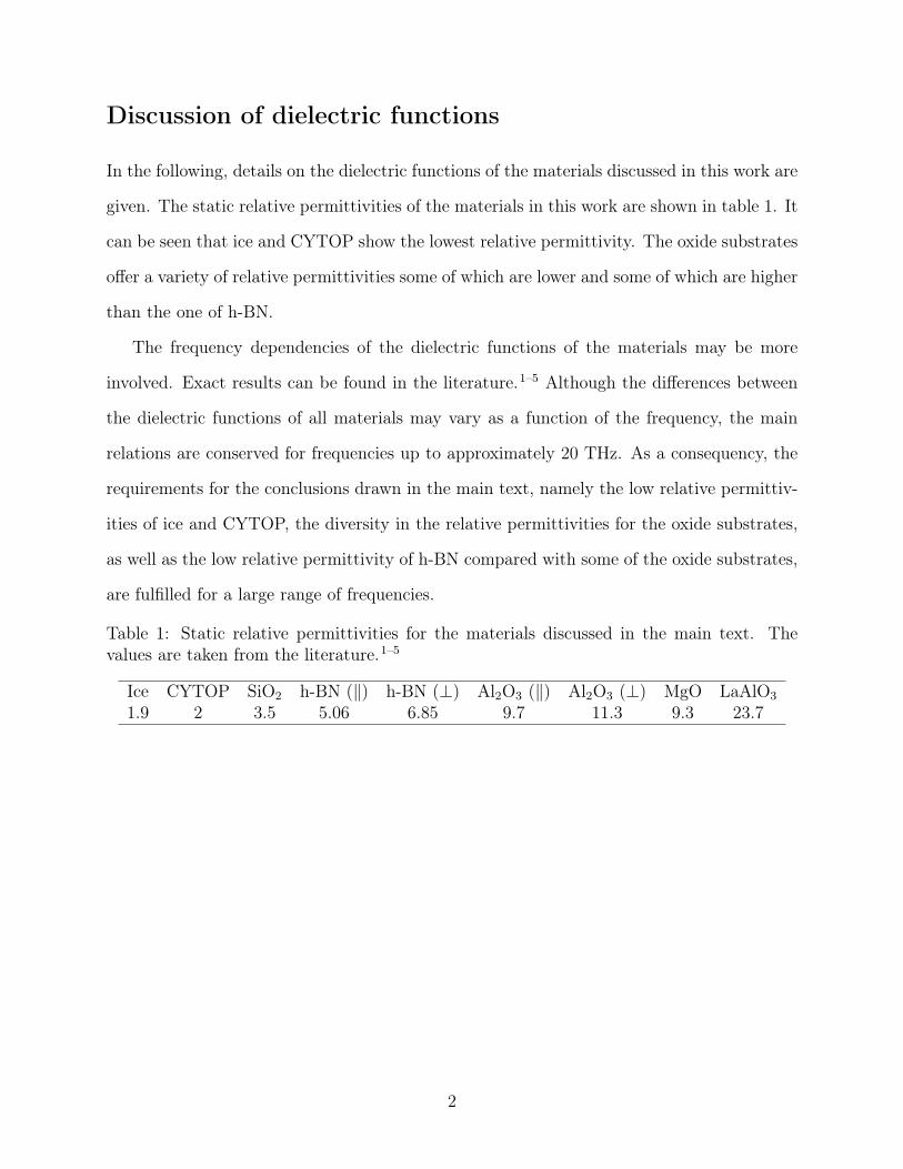
Discussion of dielectric functions
In the following, details on the dielectric functions of the materials discussed in this work are
given. The static relative permittivities of the materials in this work are shown in table 1. It
can be seen that ice and CYTOP show the lowest relative permittivity. The oxide substrates
offer a variety of relative permittivities some of which are lower and some of which are higher
than the one of h-BN.
The frequency dependencies of the dielectric functions of the materials may be more
involved. Exact results can be found in the literature.1–5 Although the differences between
the dielectric functions of all materials may vary as a function of the frequency, the main
relations are conserved for frequencies up to approximately 20 THz. As a consequency, the
requirements for the conclusions drawn in the main text, namely the low relative permittiv-
ities of ice and CYTOP, the diversity in the relative permittivities for the oxide substrates,
as well as the low relative permittivity of h-BN compared with some of the oxide substrates,
are fulfilled for a large range of frequencies.
Table 1: Static relative permittivities for the materials discussed in the main text. Thevalues are taken from the literature.1–5
Ice CYTOP SiO2 h-BN (‖) h-BN (⊥) Al2O3 (‖) Al2O3 (⊥) MgO LaAlO3
1.9 2 3.5 5.06 6.85 9.7 11.3 9.3 23.7
2
Figure 9.

14
Nano-bubbles in van-der-Waals heterostructures
Figure 1: Scanning electron microscope image of a WSe2 ML (yellow dashed line) placed ona h-BN flake (blue dashed line). Black spots can be observed at the van-der-Waals interfacebetween the two materials. The black spots represent agglomerations of foreign materialtrapped at the van-der-Waals interface. It is apparent that the contamination only covers asmall fraction of the entire sample area. The scale bar is 10µm.
3
Figure 10.

15
Gate dependent photoluminescence experiment for differ-
ent dielectric environments
0 counts max
1.5 1.6 1.70
50
100
energy [eV]
0
50
100
gate
volt
age
[V] 0
50
100
1.6
1.62
1.64
1.66
emis
sion
ener
gy[eV
]
vacuum
SiO2
vacuum
h-BN
h-BN
h-BN
0 20 40 60 80 100
26
30
34
gate voltage [V]
ET
[meV
]
vacuum
SiO2
ǫ = 2.5
vacuum
h-BN
ǫ = 3.9
h-BN
h-BN
ǫ = 6.9
X
X−
X+
X
X− X
X−
a) b)
c)
Figure 2: Gate dependent photoluminescence of a MoSe2 ML in different dielectric environ-ments. a) shows the photoluminescence signal as a function of the applied gate voltage. Inall three dielectric environments, the negatively charged trion and the neutral exciton can beobserved. On SiO2, the positively charged trion can be observed as well. The white dashedlines mark gate voltages where the signal of the neutral exciton emission forms 5% of thetotal intensity. b) Emission energies of the neutral exciton (solid lines) and the trion (dashedlines) as a function of the applied gate voltage. c) Trion binding energy as a function of theapplied gate voltage. The marks in b) and c) mark the gate voltages where the signal of theneutral exciton emission forms 5% of the total intensity.
4
Figure 11.

16
Data analysis tool Py2DSpectroscopy
The hyperspectral data acquired in this work was analyzed using a home-developed analysis
tool written in Python called Py2DSpectroscopy (figs. 3 and 4). The tool enables to browse
hyperspectral data, align micrographs (e. g. AFM or SEM) with the data and fit the spectra
included in the data. The source code is available on GitHub.6
Figure 3: Browsing hyperspectral data using the Py2DSpectroscopy tool. The screenshotshows a colorplot of the integrated photoluminescence signal from a MoSe2 monolayer on aLaAlO3 substrate in the right window, as well as the spectrum at a specific position of thesample in the left window.
Figure 4: Fitting hyperspectral data using the Py2DSpectroscopy tool. The screenshotshows the fitting tool window on the left, as well as a colormap of the fitted emission energyof the trion from the same sample as in fig. 3 in the right window.
5
Figure 12.

17
References
(1) Kobayashi, K. Optical spectra and electronic structure of ice. J. Phys. Chem. 1983, 87,
4317–4321.
(2) Bellex. http://www.bellexinternational.com/products/cytop/, Accessed: 2017-05-
19.
(3) Geick, R.; Perry, C. H.; Rupprecht, G. Normal Modes in Hexagonal Boron Nitride. Phys.
Rev. 1966, 146, 543.
(4) Aspnes, D. E.; Theeten, J. B. Dielectric function of Si-SiO2 and Si-Si3N4 mixtures.
Journal of Applied Physics 1979, 50, 4928.
(5) Krupka, J.; Geyer, R.; Kuhn, M.; Hinken, J. Dielectric properties of single crystals of
Al2O3, LaAlO3, NdGaO3, SrTiO3, and MgO at cryogenic temperatures. IEEE Transac-
tions on Microwave Theory and Techniques 1994, 42, 1886–1890.
(6) SvenBo90/Py2DSpectroscopy: A simple Python UI script that can be used for the anal-
ysis of spectroscopy measurements on 2D materials, such as MoS2. https://github.
com/SvenBo90/Py2DSpectroscopy, Accessed: 2017-05-19.
6
Figure 13.


![C 6 Theory of Scanning Tunneling Microscopy1 - arXiv · PDF filearXiv:1404.0961v1 [cond-mat.mes-hall] 3 Apr 2014 C 6 Theory of Scanning Tunneling Microscopy1 S. Lounis Peter Gru¨nberg](https://img.dokumen.tips/doc/110x75/5a731d727f8b9aa7538e444a/c-6-theory-of-scanning-tunneling-microscopy1-arxiv-a-arxiv14040961v1-cond-matmes-hall.jpg)


![On asymptotics, Stirling numbers, Gamma function and ... · arXiv:math/0607514v1 [math.CO] 20 Jul 2006 On asymptotics, Stirling numbers, Gamma function and polylogs Daniel B. Gru¨nberg](https://img.dokumen.tips/doc/110x75/5d59b1ee88c993f3188b5f01/on-asymptotics-stirling-numbers-gamma-function-and-arxivmath0607514v1.jpg)