Embed Size (px)
Citation preview

Energy-Efficient Digital Signal Processing Hardware Design
by
Dongsuk Jeon
A dissertation submitted in partial fulfillmentof the requirements for the degree of
Doctorate of Philosophy(Electrical Engineering)
in the University of Michigan2014
Doctoral Committee:
Professor Dennis M. Sylvester, ChairProfessor David BlaauwProfessor Katsuo KurabayashiAssistant Professor Zhengya Zhang

c© Dongsuk Jeon
All Rights Reserved
2014

To God and my family
with love and gratitude
ii

ACKNOWLEDGEMENTS
I have been very fortunate to meet great people along the way. Many people have helped me
throughout my Ph.D., but no one was more crucial than my advisor, Prof. Dennis Sylvester. Since
I started this journey not knowing the way forward, he has guided me with insightful advice in
many aspects. Without his continuous support and encouragement, I would have never completed
any project in this dissertation. What I have learned from him is not limited to circuit designs, but
spans over how to look at the big picture and manage research. I am also very indebted to Prof.
David Blaauw for his insightful feedbacks. He has always been enthusiastic whenever I wanted to
discuss about technical details and new ideas, and gladly given invaluable advice about the things
that can be easily disregarded. I also would like to thank other committee members, Prof. Zhengya
Zhang and Katsuo Kurabayashi for their key questions and helpful feedbacks. I would especially
like to thank Zhengya for being a great mentor and sharing his experience as a senior in DSP
hardware design area. Prof. Chaitali Chakrabarti also provided lots of help in the FFT processor
design in Chapter 2.
Most works in this dissertation were completed through much support from the industry. STMi-
croelectronics and TSMC have generously provided chip fabrication, and Samsung Scholarship
Foundation has provided financial support for the entire period. During summer internships at
Texas Instruments and imec, I met many great mentors including Manish Goel, Seok-Jun Lee from
TI, Refet Firat Yazicioglu and Hyejung Kim from imec who all inspired me with their expertise in
various areas.
I am indebted to many of my colleagues for their help and advice during my time at Michigan.
I worked closely with Mingoo Seok in the FFT project in Chapter 2, and he taught me nearly
everything about digital circuit design. I am grateful to Yejoong Kim for many discussions and his
help in other 3 projects in Chapter 4, 5 and 6. I enjoyed working with Yen-Po Chen and Qing Dong
iii

whose help was crucial in the ECG and face recognition projects. I also thank other co-authors,
Yoonmyung Lee, Inhee Lee, Michael Henry and Zhiyoong Foo for their crucial help. I need to say
that Prof. Hao Yu, Prof. Tony Tae-Hyoung Kim, Xiaolong Wang and Shuai Chen made my time
at NTU in Singapore an invaluable research experience.
Since joining our research group, I have had a great time with fellow students here. I have
learned a lot about circuit design and related knowledge from Jae-sun Seo, Daeyeon Kim, David
Fick, Michael Wieckowski, Sudhir Satpathy, Matt Fojtik, Bharan Giridhar, Gyouho Kim, Dong-
min Yoon, Nathaniel Pinckney, Suyoung Bang, Laura Freyman, Seok-Hyeon Jeong, Sechang Oh,
Myungjoon Choi, Taekwang Jang, and Wootaek Lim.
Finally, but not least, I am very grateful to my family for their continuous support throughout
my graduate study.
iv

TABLE OF CONTENTS
DEDICATION . . . . . . . . . . . . . . . . . . . . . . . . . . . . . . . . . . . . . . . . . ii
ACKNOWLEDGEMENTS . . . . . . . . . . . . . . . . . . . . . . . . . . . . . . . . . . iii
LIST OF FIGURES . . . . . . . . . . . . . . . . . . . . . . . . . . . . . . . . . . . . . . vii
LIST OF TABLES . . . . . . . . . . . . . . . . . . . . . . . . . . . . . . . . . . . . . . . x
CHAPTER
1 Introduction . . . . . . . . . . . . . . . . . . . . . . . . . . . . . . . . . . . . . 11.1 Voltage Scaling . . . . . . . . . . . . . . . . . . . . . . . . . . . . . . . 21.2 Timing Error Management . . . . . . . . . . . . . . . . . . . . . . . . . 41.3 Architecture and Algorithm Optimization . . . . . . . . . . . . . . . . . . 51.4 Dissertation Overview . . . . . . . . . . . . . . . . . . . . . . . . . . . . 6
2 Energy-Optimized FFT Processor . . . . . . . . . . . . . . . . . . . . . . . . . . 92.1 Introduction . . . . . . . . . . . . . . . . . . . . . . . . . . . . . . . . . 92.2 Energy-optimal FFT Architecture . . . . . . . . . . . . . . . . . . . . . . 11
2.2.1 Modified R4MDC architecture . . . . . . . . . . . . . . . . . . . 122.2.2 Parallel-pipelined architecture . . . . . . . . . . . . . . . . . . . 14
2.3 Robust Subthreshold FIFO Design . . . . . . . . . . . . . . . . . . . . . 162.4 Clock Distribution Network . . . . . . . . . . . . . . . . . . . . . . . . . 192.5 Measurement Results . . . . . . . . . . . . . . . . . . . . . . . . . . . . 212.6 Conclusions . . . . . . . . . . . . . . . . . . . . . . . . . . . . . . . . . 24
3 Design Methodology for Voltage Overscaled Ultra-Low Power Systems . . . . . . 253.1 Introduction . . . . . . . . . . . . . . . . . . . . . . . . . . . . . . . . . 253.2 Related Work . . . . . . . . . . . . . . . . . . . . . . . . . . . . . . . . 26
3.2.1 Error-tolerant DSP applications . . . . . . . . . . . . . . . . . . . 263.2.2 Design approach for voltage overscaled systems . . . . . . . . . . 27
3.3 Error Analysis in Voltage Overscaled Systems . . . . . . . . . . . . . . . 273.3.1 Ripple carry adder starting point . . . . . . . . . . . . . . . . . . 283.3.2 Generalized critical path delay model . . . . . . . . . . . . . . . 303.3.3 Model verification with pipelined Baugh-Wooley multipliers . . . 31
v

3.4 Case Study: Error-Resilient K-Best Decoder . . . . . . . . . . . . . . . . 363.5 Conclusions . . . . . . . . . . . . . . . . . . . . . . . . . . . . . . . . . 41
4 Energy-Optimized Feature Extraction Accelerator . . . . . . . . . . . . . . . . . 434.1 Introduction . . . . . . . . . . . . . . . . . . . . . . . . . . . . . . . . . 434.2 Proposed Visual Feature Extraction Algorithm . . . . . . . . . . . . . . . 44
4.2.1 Visual feature extraction . . . . . . . . . . . . . . . . . . . . . . 444.2.2 Proposed hardware-oriented feature extraction algorithm . . . . . 46
4.3 Energy-Efficient Hardware Architecture . . . . . . . . . . . . . . . . . . 514.3.1 Accelerator architecture . . . . . . . . . . . . . . . . . . . . . . . 514.3.2 Parallelized filters and arithmetic blocks . . . . . . . . . . . . . . 544.3.3 Single stream descriptor . . . . . . . . . . . . . . . . . . . . . . . 56
4.4 Latch-based Low-Power and Robust FIFO Design . . . . . . . . . . . . . 584.5 Measurement Results . . . . . . . . . . . . . . . . . . . . . . . . . . . . 654.6 Conclusions . . . . . . . . . . . . . . . . . . . . . . . . . . . . . . . . . 67
5 Implantable ECG Monitoring System . . . . . . . . . . . . . . . . . . . . . . . . 685.1 Introduction . . . . . . . . . . . . . . . . . . . . . . . . . . . . . . . . . 685.2 Proposed ECG Monitoring System . . . . . . . . . . . . . . . . . . . . . 695.3 Hardware design and optimization techniques . . . . . . . . . . . . . . . 71
5.3.1 Analog front end optimization . . . . . . . . . . . . . . . . . . . 715.3.2 Digital back end design . . . . . . . . . . . . . . . . . . . . . . . 73
5.4 Measurement Results . . . . . . . . . . . . . . . . . . . . . . . . . . . . 795.5 Conclusions . . . . . . . . . . . . . . . . . . . . . . . . . . . . . . . . . 84
6 Low-power Face Detection and Recognition Accelerator . . . . . . . . . . . . . . 856.1 Introduction . . . . . . . . . . . . . . . . . . . . . . . . . . . . . . . . . 856.2 Face Detection and Recognition Algorithm . . . . . . . . . . . . . . . . . 876.3 Proposed Hardware Architecture . . . . . . . . . . . . . . . . . . . . . . 886.4 Write-Once Read-Only 5T SRAM . . . . . . . . . . . . . . . . . . . . . 916.5 Implementation . . . . . . . . . . . . . . . . . . . . . . . . . . . . . . . 976.6 Conclusions . . . . . . . . . . . . . . . . . . . . . . . . . . . . . . . . . 97
7 Conclusions . . . . . . . . . . . . . . . . . . . . . . . . . . . . . . . . . . . . . 98
BIBLIOGRAPHY . . . . . . . . . . . . . . . . . . . . . . . . . . . . . . . . . . . . . . . 100
vi

LIST OF FIGURES
Figure1.1 ARM Cortex-M4 processor architecture optimized for digital signal processing
applications [3]. . . . . . . . . . . . . . . . . . . . . . . . . . . . . . . . . . . . . 21.2 Simulated energy as a function of power supply voltage [10]. . . . . . . . . . . . . 21.3 Process variation in SRAM hold noise margin in super and sub-threshold operation
regions [11]. . . . . . . . . . . . . . . . . . . . . . . . . . . . . . . . . . . . . . . 31.4 Basic Razor flip-flop [13]. . . . . . . . . . . . . . . . . . . . . . . . . . . . . . . 41.5 Algorithmic noise tolerance technique [15]. . . . . . . . . . . . . . . . . . . . . . 51.6 An example of application-specific efficient hardware architecture [7]. . . . . . . . 62.1 (a) Memory-based architecture and (b) R4MDC pipelined architecture. . . . . . . . 112.2 Modified R4MDC architecture for 1024-pt FFT. . . . . . . . . . . . . . . . . . . . 132.3 FFT core architecture with 2 processing lanes. . . . . . . . . . . . . . . . . . . . . 142.4 (a) Energy breakdown and (b) energy-area tradeoff of parallel-pipelined architec-
tures. . . . . . . . . . . . . . . . . . . . . . . . . . . . . . . . . . . . . . . . . . . 152.5 Proposed 8-word FIFO design with commutator architecture. . . . . . . . . . . . . 172.6 Readout delay distributions from 100k Monte-Carlo SPICE simulations. . . . . . . 182.7 Positive-edge read and negative-edge write scheme. . . . . . . . . . . . . . . . . . 192.8 RC-matched 3-level clock distribution network along with maximum RC mis-
match values. . . . . . . . . . . . . . . . . . . . . . . . . . . . . . . . . . . . . . 202.9 Simulated clock skew and slew rates in proposed clock network design. . . . . . . 202.10 Measured (a) energy consumption and (b) performance of the FFT core. . . . . . . 212.11 Measured performance and energy consumption as a function of temperature. . . . 222.12 Measured energy (a) and performance (b) distributions at Vdd = 300mV. . . . . . . 232.13 Die photograph of the FFT core in 65nm CMOS. . . . . . . . . . . . . . . . . . . 233.1 Critical path and an example activated path in a 32-bit ripple carry adder. . . . . . . 283.2 Error rate of RCA from simulation and proposed equation. . . . . . . . . . . . . . 293.3 Error rate considering multiple critical paths. . . . . . . . . . . . . . . . . . . . . 303.4 Fabricated un-pipelined and 5-stage pipelined multipliers in 65nm. . . . . . . . . . 323.5 Error rate quantile-clock period plot from measurements of the un-pipelined mul-
tiplier. . . . . . . . . . . . . . . . . . . . . . . . . . . . . . . . . . . . . . . . . . 323.6 Simulated and estimated error rates of various multiplier designs. . . . . . . . . . . 34
vii

3.7 µ and σ from simulation and the proposed model. . . . . . . . . . . . . . . . . . . 343.8 Measurements of un-pipelined and 5-stage pipelined multipliers. . . . . . . . . . . 353.9 Energy consumption-error rate plot from simulation. . . . . . . . . . . . . . . . . 353.10 K-best decoder architecture. . . . . . . . . . . . . . . . . . . . . . . . . . . . . . 363.11 Voltage overscaled CE assignment scheme. . . . . . . . . . . . . . . . . . . . . . 373.12 SNR-BER plot for different error rates. . . . . . . . . . . . . . . . . . . . . . . . . 383.13 Detailed CE architecture. . . . . . . . . . . . . . . . . . . . . . . . . . . . . . . . 393.14 Two different pipeline stage assignments for critical path. . . . . . . . . . . . . . . 403.15 Error rate of voltage-overscaled CEs. . . . . . . . . . . . . . . . . . . . . . . . . . 403.16 Energy-error rate tradeoffs of CE for different pipeline depths. . . . . . . . . . . . 414.1 An example of object recognition using extracted features [58]. . . . . . . . . . . . 444.2 Two key constraints of feature extraction algorithms: (a) rotation and (b) scale
invariance. . . . . . . . . . . . . . . . . . . . . . . . . . . . . . . . . . . . . . . . 454.3 Original feature vector generation process consisting of (a) orientation assignment
and (b) feature vector generation [59]. . . . . . . . . . . . . . . . . . . . . . . . . 454.4 A target application of MAV with visual navigation. . . . . . . . . . . . . . . . . . 474.5 An overview of the visual navigation algorithm flow. . . . . . . . . . . . . . . . . 474.6 Proposed (a) single-octave scale space; and (b) fast localization techniques for
detector optimization. . . . . . . . . . . . . . . . . . . . . . . . . . . . . . . . . . 494.7 Proposed circular-shaped sampling region approach. . . . . . . . . . . . . . . . . 494.8 Unified description process consists of (a) filter response calculation; (b) summa-
tion in circular-shaped sampling region; and (c) reordering and normalization offeature vector. . . . . . . . . . . . . . . . . . . . . . . . . . . . . . . . . . . . . . 50
4.9 (a) Rotation; and (b) scale invariance performance comparisons. . . . . . . . . . . 514.10 Proposed feature extraction processor architecture. . . . . . . . . . . . . . . . . . 524.11 Overlapped image subsections are processed successively to allow for proper fea-
ture extraction at boundaries. . . . . . . . . . . . . . . . . . . . . . . . . . . . . . 524.12 Image summation in a rectangular region implemented with 3 arithmetic opera-
tions on a 2-D integrated image. . . . . . . . . . . . . . . . . . . . . . . . . . . . 544.13 Image summation calculators based on (a) a single datapath with memory and (b)
multiple arithmetic units with different delay elements. . . . . . . . . . . . . . . . 544.14 Unrolled 2-D image integrator architecture. . . . . . . . . . . . . . . . . . . . . . 554.15 (a) Original and (b) proposed local maxima detection schemes. In (b), maximum
point of each row is already stored and only one comparison per row is required. . . 564.16 (a) Conventional multi-core architecture where each core communicates through a
shared data bus independently. (b) Proposed architecture where a single responseflows continuously through shared data bus and each core reads in only its requiredblocks. . . . . . . . . . . . . . . . . . . . . . . . . . . . . . . . . . . . . . . . . . 57
4.17 Proposed single-lane shift latch propagating data and a bubble in opposite direc-tions at each cycle. . . . . . . . . . . . . . . . . . . . . . . . . . . . . . . . . . . 60
4.18 A one-output-per-cycle FIFO consisting of N lanes and shared readout circuitry. . . 614.19 An 8-bit 840-entry FIFO based on the proposed shift-latch architecture. . . . . . . 61
viii

4.20 (a) Worst-case scenario for leakage current affecting bitline pull-down with andwithout leakage compensation technique. (b) Proposed 2-transistor AND gates. . . 62
4.21 Simulated (a) delay, area, and (b) energy consumption of baseline and proposedFIFO designs as a function of FIFO size. . . . . . . . . . . . . . . . . . . . . . . . 63
4.22 Simulated energy savings in each component of a 1k-entry FIFO. . . . . . . . . . . 634.23 A microphotograph of the fabricated feature extraction accelerator and summary
table. . . . . . . . . . . . . . . . . . . . . . . . . . . . . . . . . . . . . . . . . . . 644.24 Measurement results across different operating voltages. . . . . . . . . . . . . . . 654.25 A sample image marked with 1421 extracted features from measurements. . . . . . 665.1 Overview of syringe implantable ECG monitoring system. . . . . . . . . . . . . . 705.2 Monitoring device implanted near the heart. . . . . . . . . . . . . . . . . . . . . . 705.3 Usage scenario of the proposed system. . . . . . . . . . . . . . . . . . . . . . . . 715.4 Proposed SoC in a 14 gauge syringe needle. . . . . . . . . . . . . . . . . . . . . . 715.5 Tradeoffs between (a) input referred noise and current consumption, and (b) detec-
tion accuracy and input referred noise. . . . . . . . . . . . . . . . . . . . . . . . . 725.6 Arrhythmia detection in a moving 10-second window. . . . . . . . . . . . . . . . . 735.7 Time domain detection algorithm. . . . . . . . . . . . . . . . . . . . . . . . . . . 745.8 Frequency domain detection algorithm. . . . . . . . . . . . . . . . . . . . . . . . 745.9 Overview of the proposed digital back end design. . . . . . . . . . . . . . . . . . . 755.10 Proposed 512-point real-valued FFT accelerator. . . . . . . . . . . . . . . . . . . . 765.11 Proposed minimum energy computation technique applied to the FDM block. . . . 775.12 Die photo of the proposed SoC and summary table. . . . . . . . . . . . . . . . . . 785.13 Measurement results from ECG simulator test. . . . . . . . . . . . . . . . . . . . . 795.14 Human body test. . . . . . . . . . . . . . . . . . . . . . . . . . . . . . . . . . . . 805.15 Implantation environment test with live sheep heart. . . . . . . . . . . . . . . . . . 805.16 Overview of the complete system configuration. . . . . . . . . . . . . . . . . . . . 825.17 Macro-scale test setup with control, decap and radio layers. . . . . . . . . . . . . . 836.1 Applications for real-time face detection and recognition system. . . . . . . . . . . 866.2 Proposed face detection and recognition system flow. . . . . . . . . . . . . . . . . 876.3 Proposed face detection and recognition system architecture. . . . . . . . . . . . . 886.4 Proposed architecture optimization techniques. . . . . . . . . . . . . . . . . . . . 906.5 Proposed 5T bit cell and basic write operation. . . . . . . . . . . . . . . . . . . . . 916.6 Layout of the proposed 5T bit cell. . . . . . . . . . . . . . . . . . . . . . . . . . . 926.7 Reset sequence of the proposed design. . . . . . . . . . . . . . . . . . . . . . . . 936.8 Write sequence of the proposed design. . . . . . . . . . . . . . . . . . . . . . . . 946.9 Read energy consumption of the proposed 5T and conventional 6T designs. . . . . 956.10 Implemented face detection and recognition accelerator. . . . . . . . . . . . . . . . 96
ix

LIST OF TABLES
Table2.1 Characteristics of published FFT cores and the proposed design. . . . . . . . . . . 244.1 Comparisons of prior works and proposed design. . . . . . . . . . . . . . . . . . . 665.1 Comparisons of prior works and the proposed design. . . . . . . . . . . . . . . . . 81
x

CHAPTER 1
Introduction
As CMOS technology developed rapidly in the last few decades, various systems on chips
(SoCs) have been implemented across different applications due to reduced area and power re-
quirements. Digital signal processing (DSP) algorithms are frequently employed in these systems
to achieve more accurate estimation or faster computation. However, CMOS technology scaling
started to slow down recently and relatively large systems consume too much power to solely rely
on the scaling effect while system power budget such as battery capacity improves slowly. In addi-
tion, there exist increasing needs for miniaturized computing systems including sensor nodes that
can accomplish similar operations with significantly smaller power budget [1][2].
Due to continuous technology scaling and advances in circuit design techniques, various gen-
eral purpose cores now provide significantly improved energy efficiency while still providing flex-
ibility necessary for versatile systems (Fig. 1.1). In addition. application-driven optimizations
such as instruction set selection and architecture modification have been successfully applied to
complex SoCs [4]. However, the need for supporting even more complicated algorithm is grow-
ing in multimedia and wireless communication applications [5]. For instance, references [6] and
[7] propose energy-efficient reconfigurable accelerator designs aimed for multimedia applications.
Authors in [8] describe a LDPC decoder design with fine-grained dynamic clock gating that re-
duces switching energy. Significant amount of energy savings shown in these works mainly result
from architecture optimization and circuit techniques. This dissertation will expand the scope into
multiple design levels ranging from circuit technique to algorithmic modification and study various
energy efficiency improvement techniques.
1

Figure 1.1: ARM Cortex-M4 processor architecture optimized for digital signal processing appli-cations [3].
1.1 Voltage Scaling
There have been many research activities on different circuit techniques to enhance power ef-
ficiency, but voltage scaling is one of the most widely used low power techniques since it reduces
switching power consumption dramatically. However, leakage energy consumption increases si-
multaneously due to longer clock period and there exists theoretical limit on obtainable energy
efficiency due to increasing leakage power consumption [9].
Figure 1.2: Simulated energy as a function of power supply voltage [10].
2

Figure 1.3: Process variation in SRAM hold noise margin in super and sub-threshold operationregions [11].
Fig. 1.2 shows simulated energy consumption of an inverter chain as a function of power supply
voltage. The left plot confirms that as the supply voltage drops leakage energy starts to increase
fast at some point while switching energy reduces continuously at the same rate. The total energy
dissipation per operation is simply the summation of leakage and switching energy integrated over
each cycle and its trend is described in the right plot. The total energy reaches the minimum point
below 0.3V and increases again after that. This minimum point (or optimal point) represents the
minimum possible energy consumption one can achieve for the given system.
In addition, low supply voltage incurs significant amount of PVT variation, which requires
additional compensation circuitry and design overheads. In Fig. 1.3, it is observed that the dis-
tribution of SRAM hold noise margin becomes significantly wider as the supply voltage changes
from 1.2V (super-threshold) to 0.3V (sub-threshold). This issue makes it difficult to design a ro-
bust SRAM operating at lower operating voltages and various variants of SRAM bitcell such as
8T, 10T and 12T have been proposed to achieve better reliability. It also affects the operation of
digital logic circuits and the variation translates to the fluctuation in the critical path delay, which
3

Figure 1.4: Basic Razor flip-flop [13].
necessitates larger amount of timing margins to guarantee correct circuit operation [12].
1.2 Timing Error Management
To mitigate increased variability in low operating voltage and remove consequent timing errors
of the system, various error correction circuit techniques have been proposed in the last decade.
Fig. 1.4 shows a basic Razor flip-flop that can detect a timing error caused by tight timing margin.
The shadow latch observes the incoming data based on the delayed clock signal and checks if
there is any data change in the observation window. This simple circuit can detect a timing error
effectively without causing large hardware overhead.
Error correction circuitry such as variants of Razor [13][14] can detect certain amount of timing
errors and force entire system to halt and re-perform that operation, which leads to operation at
lower operating voltage than conventional optimal point. Although it guarantees correct operation
by correcting all errors, generally only small amount of voltage margin may be achieved since the
overhead from error correction starts to exceed the benefit of reduced energy. In other words, the
amount of savings that can be achieved from timing error correction circuit is still limited since the
correction overhead exceeds the benefit of deeper voltage scaling when the error rate is high.
4

Figure 1.5: Algorithmic noise tolerance technique [15].
Alternatively, it is also possible to take advantage of error correction scheme by decreasing
operating voltage even further below nominal operation range for better energy efficiency, which
is called ”voltage overscaling”. Voltage overscaled systems usually employ architecture or algo-
rithm level techniques to deal with significantly increased timing error rate. Since reduced clock
period causes timing errors mainly in critical paths, it is important to ensure correct operation and
outcome in those paths. The block diagram in Fig. 1.5 shows an example of architecture and algo-
rithm level technique called ANT (Algorithmic Noise Tolerance). Instead of detecting all timing
errors in the critical paths and correcting them at the expense of additional operations, it has an
additional estimator block that produces similar, but lower accuracy results than the main com-
putation block. The decision block observes the outputs from the main block and the estimator,
and if the difference exceeds a pre-defined threshold value, it takes the estimator output instead,
which guarantees operations with certain accuracy. This allows large amount of energy savings by
compensating for relatively high error rate. However, this technique can be applied only to certain
type of digital signal processing hardwares with simple architecture and few dominating blocks in
terms of energy consumption.
1.3 Architecture and Algorithm Optimization
A large amount of efficiency improvement may be also obtained by optimization techniques
in architecture and algorithm levels. Reference [7] proposes an efficient hardware architecture
that targets computational photography such as High-Dynamic Range (HDR) imaging and Low-
Light Enhanced (LLE) imaging. This provides a good example of architecture optimization with
the given algorithm (Fig. 1.6). On the other hand, algorithm optimization may enable substantial
5

Figure 1.6: An example of application-specific efficient hardware architecture [7].
improvement in overall energy efficiency. Many systems allow small amount of accuracy or quality
degradation where it introduces large amount of energy savings. Reference [16] proposes a motion
estimation processor with algorithm and architecture co-optimization. It successfully demonstrates
significant amount of power savings along with performance improvement. Due to low sensitivity
of human eye to small color or brightness changes, especially computer vision and video codec
algorithms have the potential of large energy savings.
1.4 Dissertation Overview
This dissertation seeks to mitigate excessive power consumption of conventional DSP algo-
rithm implementations by proposing various DSP hardware design approaches targeted for power-
constrained systems. First, a fast fourier transform (FFT) accelerator is studied as one of the key
parts in various DSP algorithms in Chapter 2. Along with energy-efficient FIFO for subthresh-
old operation, various FFT hardware architectures are analyzed in terms of energy efficiency. A
parallel-pipelined architecture is proposed, which suppresses leakage energy by ensuring full uti-
lization of functional units and reduces memory size. These techniques are applied to a 16-b
6

1024-pt complex-valued Fast Fourier Transform (FFT) core along with low-power first-in first-out
(FIFO) design and robust clock distribution network.
Chapter 3 takes a closer look at the properties of pipelining in ULV regime and search for the-
oretical limit of energy efficiency for the given operations. Energy savings from deep pipelining
is promising in ultra-low voltage (ULV) regime, but as scaling down continues its benefit starts
to saturate and implementation overheads may increase rapidly depending on hardware topology.
Energy efficiency gains in the subthreshold regime are limited by exponentially increasing cycle
times, and hence leakage energy. Voltage overscaling lowers circuit operating voltage aggres-
sively, leading to an overall improvement in energy efficiency in applications that can tolerate
errors. Based on simple and intuitive mathematical model, a design methodology for voltage-
overscaling of ultra-low power systems in ULV regime is proposed. First, a probabilistic model of
error rate increase is proposed for basic arithmetic units, and it is validated using both simulations
and measurements. This model allows the estimation of energy savings for the given amount of er-
ror tolerance. The model is then applied to a modified K-best decoder that employs error tolerance
to reveal the potential benefit of the framework. With simple modifications, the conventional K-
best decoder is improved to obtain noticeable error tolerance of child node expansion modules with
minimal SNR degradation while the resulting design does not require additional error-correction
circuits and employs only simple timing error-detection circuitry.
Chapter 4 proceeds to higher level approach for energy efficient hardware design. For recent
highly complicated DSP algorithms, there still exists a large room for further energy reductions.
In other words, hardware-oriented algorithm optimization may provide significant savings while
maintaining identical or similar algorithm quality. This chapter presents an energy-efficient feature
extraction accelerator design aimed for visual navigation. The hardware-oriented algorithmic mod-
ifications such as circular-shaped sampling region and unified description are proposed to minimize
area and energy consumption while maintaining feature extraction quality. A matched-throughput
accelerator architecture employs fully unrolled filter architectures and single stream descriptor ar-
chitecture enabled by algorithm-architecture co-optimization. This provides significantly larger
headroom for aggressive voltage scaling with the given throughput requirement and reduces the
hardware cost of description processing elements. Due to a large number of FIFO blocks required,
a robust low-power FIFO architecture for ULV regime is also proposed. Based on shift-latch de-
7

lay elements and balanced-leakage readout technique, it achieves noticeable energy savings and
delay reduction. These techniques are applied to feature extraction accelerator which can process
30fps VGA video in real time and it is fabricated in 28nm LP CMOS technology. The resulting
design provides significantly better energy efficiency than current state-of-the-art while extracting
features from entire image.
Chapter 5 moves the focus to a system level energy optimization and describes a highly power-
constrained ECG monitoring system. Recent complicated SoCs often include both analog and
digital domain components and the energy consumption of each block should be considered alto-
gether to maximize energy efficiency. This chapter shows that the system level noise optimization
and circuit techniques in the analog front end enable 31nA current consumption and minimum
energy computation approach in the digital back end further reduces the energy by 40%. Duty
cycling is studied as an alternate approach to reduce power consumption in the digital processing
block when original performance-driven minimum frequency and voltage operating point are be-
low minimum energy point (MEP). To mitigate various types of noise and irregularity in the ECG
signal, two different algorithms are implemented while each can be power-gated independently
depending on the environment. The proposed system achieves more than 100× power saving over
prior works.
Finally, Chapter 6 advances both architecture and circuit techniques. This chapter proposes
a single-chip solution for face detection and recognition problem. Machine learning algorithms
including SVM (Support Vector Machine) are transformed into feasible forms for hardware imple-
mentation. Since the memory blocks occupy most of the area and dominates the systems in terms
of power consumption, a write-once read-only memory based on a new 5T bit cell is proposed.
The resulting hardware can process 5fps HD video with a low clock frequency of 81MHz while
consuming only 21.7mW power.
8

CHAPTER 2
Energy-Optimized FFT Processor
2.1 Introduction
Recently, voltage scaling has been widely applied to highly energy-constrained systems such
as battery-powered sensor nodes to minimize energy consumption. Voltage scaling enables en-
ergy efficient computation by quadratic (or greater) reductions of switching and leakage power
dissipation. Although voltage scaling increases gate delay and thus degrades performance, it is
still advantageous for many applications with relaxed performance requirements [1][17] and the
supply voltage may be scaled down to, or below, the device threshold voltage Vth. However, leak-
age energy consumption per cycle increases due to enlarged stage delay as voltage scales and this
overhead starts to exceed the switching energy savings below the optimal operating point Vopt ,
producing optimal energy consumption Eopt . Therefore there exists a fundamental limit for energy
savings from voltage scaling in the subthreshold regime regardless of Vth [9]. To enhance energy
efficiency beyond this point, leakage energy must be suppressed by elimination of idle gates or
other techniques to boost the utilization of each gate or module in the system. Since ultra-low volt-
age operation incurs high process/voltage/temperature (PVT) variation [18], variation tolerance
should also be considered in designing these low voltage systems. Such an energy-optimal design
methodology is demonstrated on a FFT (Fast Fourier Transform) accelerator in this chapter.
The Fast Fourier Transform (FFT) is a key digital signal processing (DSP) algorithm and is
widely used in digital communication and sensor signal processing. Aided by technology scaling,
FFT accelerators have become feasible, offering higher energy efficiency than general purpose pro-
9

cessors even for volume-constrained systems such as sensor nodes [17][19]. Such an FFT core is
used as a demonstration vehicle for circuit and architectural techniques aimed at reducing Vopt and
Eopt , while achieving unusually high throughput for a subthreshold circuit. Past work in power
efficient FFTs include [20], where the authors propose a cached-memory FFT architecture that
processes intermediate results within cached data sets to minimize the number of main memory
accesses. In [19], the authors employ voltage scaling to improve energy efficiency. They use stan-
dard cells and memories optimized for subthreshold operation and target their design at the optimal
energy operating point. However, the body of prior work in this area has not investigated the key
role of leakage energy in the subthreshold regime, and it will be shown that energy efficiency
can be improved beyond the conventional optimal energy operating point by suppressing leakage
effectively.
This chapter describes the use of circuit techniques with an architectural study focused on ex-
tending voltage scalability and enhancing performance in the design of 1024-point complex-valued
FFT core. A parallel-pipelined FFT architecture is proposed to maximize computational element
and memory utilization, while reducing memory size and overall leakage energy. Such an ap-
proach is ideally suited to subthreshold design where leakage energy is significant, in contrast to
traditional superthreshold design paradigm where dynamic energy and performance are the pri-
mary metrics. An energy-efficient FIFO block targeted for robust operation in subthreshold regime
is also proposed. Combining these techniques, the parallel-pipelined FFT core with pipelined CEs
(computational elements) is fabricated in a standard 65nm CMOS process. The resulting design
achieves 15.8 nJ/FFT operating at 30 MHz with Vdd = 270 mV, enabling throughput of 240 Msam-
ples/s.
As a joint project with Mingoo Seok, he proposed a power saving technique called ”super
pipelining” that employs significantly more pipelining stages than conventional low voltage de-
signs to suppress leakage energy by shortening clock period. Computational blocks including
adders and multipliers are implemented using this technique, which also contributes to power sav-
ing.
10
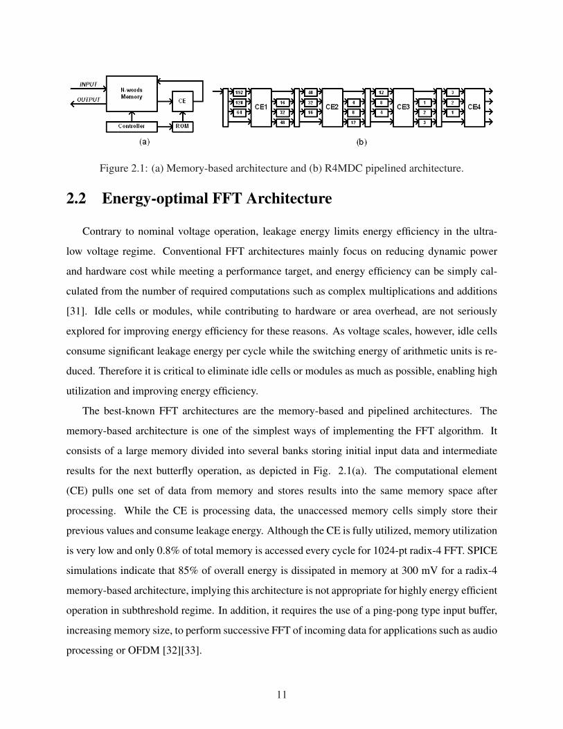
Figure 2.1: (a) Memory-based architecture and (b) R4MDC pipelined architecture.
2.2 Energy-optimal FFT Architecture
Contrary to nominal voltage operation, leakage energy limits energy efficiency in the ultra-
low voltage regime. Conventional FFT architectures mainly focus on reducing dynamic power
and hardware cost while meeting a performance target, and energy efficiency can be simply cal-
culated from the number of required computations such as complex multiplications and additions
[31]. Idle cells or modules, while contributing to hardware or area overhead, are not seriously
explored for improving energy efficiency for these reasons. As voltage scales, however, idle cells
consume significant leakage energy per cycle while the switching energy of arithmetic units is re-
duced. Therefore it is critical to eliminate idle cells or modules as much as possible, enabling high
utilization and improving energy efficiency.
The best-known FFT architectures are the memory-based and pipelined architectures. The
memory-based architecture is one of the simplest ways of implementing the FFT algorithm. It
consists of a large memory divided into several banks storing initial input data and intermediate
results for the next butterfly operation, as depicted in Fig. 2.1(a). The computational element
(CE) pulls one set of data from memory and stores results into the same memory space after
processing. While the CE is processing data, the unaccessed memory cells simply store their
previous values and consume leakage energy. Although the CE is fully utilized, memory utilization
is very low and only 0.8% of total memory is accessed every cycle for 1024-pt radix-4 FFT. SPICE
simulations indicate that 85% of overall energy is dissipated in memory at 300 mV for a radix-4
memory-based architecture, implying this architecture is not appropriate for highly energy efficient
operation in subthreshold regime. In addition, it requires the use of a ping-pong type input buffer,
increasing memory size, to perform successive FFT of incoming data for applications such as audio
processing or OFDM [32][33].
11

The pipelined architecture comprises several stages connected in series with CEs and multiple
FIFOs to store and re-order intermediate values. It leads to higher dynamic power since multiple
CEs switch simultaneously. However, CEs only access FIFOs of the previous stage, and these
FIFOs are relatively small compared to the large memory in a memory-based architecture. This
significantly reduces the average number of memory cells per CE, enabling high memory utiliza-
tion and in turn reducing memory leakage energy.
The most straightforward pipelined architecture is MDC (Multi-path Delay Commutator), shown
in Fig. 2.1(b) [34]. Each stage corresponds to one segment of the signal flow graph and the CE
performs butterfly computation in the same way as in the memory-based architecture. The com-
mutator consists of switching network and FIFOs, and re-orders the data flow for CE of next stage.
However, this architecture suffers from CE utilization as low as 25% for R4MDC (radix-4 MDC)
architecture since it accepts only one input per cycle, then waits for several cycles to build a full
set of data required for a butterfly operation. This drawback becomes worse in higher-radix FFT
algorithms since more data is required for a butterfly operation. In addition, for an N-point FFT
this architecture requires 3(log4N-1) complex multipliers and 5N/2-4 memory cells, making the
hardware costs higher than other pipelined architectures.
A widely used pipelined architecture is R22SDF (Single-path Delay Feedback) [31]. This
approach introduces a feedback path composed of local memory beside each CE to temporarily
store intermediate values rather than a large memory in the commutator module of the R4MDC
architecture. R22SDF requires log4N-1 complex multipliers and only N-1 memory cells, achieving
75% utilization of complex multipliers.
2.2.1 Modified R4MDC architecture
The conventional R4MDC architecture accepts only one input per cycle while processing 4
input data concurrently per cycle, and thus the CEs performing radix-4 butterfly operations are
activated partially to match throughput with input data rate. This incurs significant leakage energy
overhead due to low CE and memory utilization. However, if four inputs from a single channel are
obtained in one cycle, full CE utilization can be achieved, which also minimizes memory leakage
energy since the number of cycles required to perform one FFT is reduced.
12

Figure 2.2: Modified R4MDC architecture for 1024-pt FFT.
This modified R4MDC architecture with 4 inputs per cycle is depicted in Fig. 2.2. In altering
the original R4MDC architecture to achieve full utilization, several changes are made:
- Altered data scheduling within a commutator
- Different configurations for each FIFO
- Process four input data per cycle
While the original R4MDC architecture employs large input buffers to convert serial input to a
parallel data stream for the first CE, the modified architecture allows the input re-ordering buffer to
be half as large since four input data are fed into the FFT core per cycle. Therefore data scheduling
within a commutator had to be changed from the original R4MDC architecture, which results in
smaller FIFO configurations as shown in Fig. 2.2. The switching network remains the same as
the original R4MDC and a look-up table for twiddle factors is embedded in each CE along with a
controller.
In addition to full CE utilization, this architecture requires fewer memory cells for commu-
tators. Specifically, modified R4MDC contains 7N/4-4 memory cells compared to 5N/2-4 in
R4MDC, reducing memory size by 30% for a 1024-pt FFT. Although a CE accesses memory
every cycle, implying full memory utilization, this does not reflect the actual number of activated
versus idle cells. Instead the average number of memory cells per complex multiplier can be
used as an alternate metric in energy-constrained applications. For a 1024-pt FFT, the modified
R4MDC requires 149 cells per complex multiplier while R22SDF needs 255.75 cells (72% more).
Taken together, modified R4MDC achieves 4 higher throughput and more energy efficient opera-
tion than R22SDF with smaller hardware cost. Simulation results indicate that modified R4MDC
and R22SDF consume 52% and 68% of their total energy in memory at 250mV, respectively, with
modified R4MDC consuming 43.2% less energy with 2.6× better performance than R22SDF at
their respective energy-optimal points.
13

Figure 2.3: FFT core architecture with 2 processing lanes.
2.2.2 Parallel-pipelined architecture
The improvements above significantly increase memory utilization and suppress leakage en-
ergy. However, even the modified R4MDC architecture consumes 52% of its total energy in mem-
ory, indicating that further room for improvement exists in memory utilization. This section shows
that FFT architecture parallelization reduces energy consumption per operation and improves per-
formance simultaneously.
Fig. 2.3 shows the modified R4MDC architecture with 2 processing lanes in parallel. Eight
in-order input data are fed into the FFT core every cycle and each processing lane processes data
within its own data set until the 2nd stage from the last, after which intermediate results are ex-
changed followed by independent processing in each lane. The proposed design in Fig. 2.3 requires
4N/7-8 memory cells, similar to the 1-lane version. Thus, the average number of memory cells per
14

Figure 2.4: (a) Energy breakdown and (b) energy-area tradeoff of parallel-pipelined architectures.
multiplier is reduced by more than 50%, translating directly to memory leakage reduction. The
proposed design improves performance by 2× through parallelism while consuming only 35% of
its total energy in memory, indicating a greater degree of voltage scalability and potential Eopt
improvements.
Area-time-energy optimization has been applied in a FIR filter [35] previously to improve en-
ergy efficiency with fixed throughput. The proposed FFT architecture differs from this work in that
it focuses solely on achieving minimum energy consumption with emphasis on the role of leak-
age current in the subthreshold regime. Since ultra-low voltage (subthreshold) FFT architectures
consume most of their energy in memory as leakage, the enhanced memory utilization from the
proposed architecture provides significant energy savings.
The FFT core can be further parallelized to achieve continued benefits. However, hardware
costs increase while the benefit from parallelization saturates as the CE active energy starts to
dominate. Fig. 2.4(a) shows energy breakdowns of modified R4MDC architectures with different
degrees of parallelism. With the CE already fully utilized, its energy consumption remains un-
changed while memory energy decreases with additional parallelization. The energy-area tradeoff
shown in Fig. 2.4(b) clearly indicates that energy reductions from aggressive parallelism saturate
while incurring large area overhead. Although the minimum energy will be achieved when entire
signal flow of FFT algorithm is implemented without any memory modules, increased numbers
of multipliers and other modules results in higher PVT-induced variability and lower maximum
15

operating frequency, translating to more leakage energy per cycle. In addition, higher parallelism
incurs wire overheads including the switching network and input/output interfaces. Based on this
and available silicon area constraints, the 2-lane version was implemented.
Simulation results show that the proposed design with 2 lanes consumes 27.5% less energy
with 2 higher performance than a 1-lane version, translating to 2.4× better energy efficiency and
5.2× higher throughput than the conventional R22SDF architecture.
2.3 Robust Subthreshold FIFO Design
The First-in First-out (FIFO) is a key module in commutators, and the proposed architecture
employs a large number of these modules. Simulations of the 2-lane modified R4MDC architecture
show that FIFOs consume up to 29% of total energy, making it necessary to explore energy efficient
FIFO design.
The most straightforward FIFO implementation is a shift register-based FIFO [36]. For an N
delay FIFO, N registers are connected in series and all of them switch every cycle, sending data to
next stage. Although this is very robust due to its negative hold time property, registers toggling
every cycle have significant switching power overhead, making them less attractive for low power
designs. Another possible candidate for a low-power FIFO is an SRAM-based design [37], which
uses conventional SRAM for storing data and reads data from each word successively, writing
subsequent data into the same address. For nominal voltage operation, a simple 6T SRAM can
be used for high density with lower switching power than shift registers while retaining sufficient
speed to match the data rate. However, a 6T SRAM is not suitable for the subthreshold regime
due to its susceptibility to process variability and resulting small read/write margins, and variants
such as 10T [38] are preferred for robust operation. The maximum operating frequency of robust
subthreshold SRAM designs is typically below 1 MHz [39][40], making it impossible to meet
performance requirements of the target FFT design.
To mitigate these performance and variation issues, a latch-based memory is used. Although
latch-based memory as described in [19] increases read/write margins and offers potential perfor-
mance improvements, additional address generator or decoder is necessary for read/write address
signal generation. In addition, MUX-based readout paths are slow and suffer from leakage energy
16

Figure 2.5: Proposed 8-word FIFO design with commutator architecture.
17
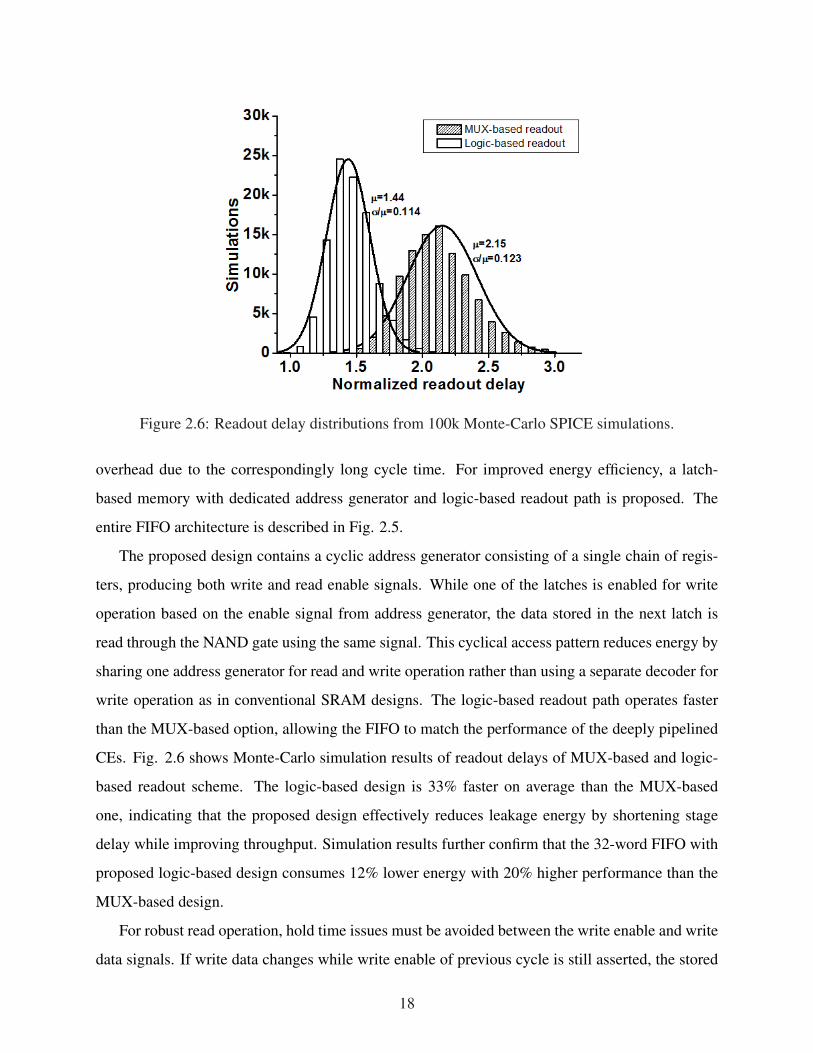
Figure 2.6: Readout delay distributions from 100k Monte-Carlo SPICE simulations.
overhead due to the correspondingly long cycle time. For improved energy efficiency, a latch-
based memory with dedicated address generator and logic-based readout path is proposed. The
entire FIFO architecture is described in Fig. 2.5.
The proposed design contains a cyclic address generator consisting of a single chain of regis-
ters, producing both write and read enable signals. While one of the latches is enabled for write
operation based on the enable signal from address generator, the data stored in the next latch is
read through the NAND gate using the same signal. This cyclical access pattern reduces energy by
sharing one address generator for read and write operation rather than using a separate decoder for
write operation as in conventional SRAM designs. The logic-based readout path operates faster
than the MUX-based option, allowing the FIFO to match the performance of the deeply pipelined
CEs. Fig. 2.6 shows Monte-Carlo simulation results of readout delays of MUX-based and logic-
based readout scheme. The logic-based design is 33% faster on average than the MUX-based
one, indicating that the proposed design effectively reduces leakage energy by shortening stage
delay while improving throughput. Simulation results further confirm that the 32-word FIFO with
proposed logic-based design consumes 12% lower energy with 20% higher performance than the
MUX-based design.
For robust read operation, hold time issues must be avoided between the write enable and write
data signals. If write data changes while write enable of previous cycle is still asserted, the stored
18

Figure 2.7: Positive-edge read and negative-edge write scheme.
data of previous latch will be corrupted. To avoid this hold time issue, it utilizes a negative-edge
write scheme. As described in Fig. 2.7, the write data signal remains unchanged for a half cycle
after the previous write enable signal is disabled to provide large write operation timing margin and
guaranteeing timing violation-free write operation. Since the readout path is critical for this FIFO
module, this increased timing margin for write operation does not impact overall performance. 8-
word and 32-word FIFOs are first implemented, and larger FIFOs are obtained by connecting them
in series.
2.4 Clock Distribution Network
Clock tree distribution networks of large integrated circuits are generally composed of several
levels with local clock buffers to suppress RC delay of long wires. In the nominal voltage regime,
clock buffer gate delay is small compared to the RC delay of global clock networks and inserting
a large number of clock buffers is used to reduce clock skew. In the subthreshold regime, however,
exponentially increased gate delay dominates while RC delay no longer contributes appreciably
to clock path delay mismatches. In contrast, buffer mismatch significantly impacts clock distri-
bution delays and adding more buffers leads to higher clock skew. Mismatch can be effectively
suppressed by employing only a small number of large buffers, since they are robust to random
process variations [18][41].
In this design, the clock network was designed with only 3 levels and a small number of rela-
19

Figure 2.8: RC-matched 3-level clock distribution network along with maximum RC mismatchvalues.
Figure 2.9: Simulated clock skew and slew rates in proposed clock network design.
20

Figure 2.10: Measured (a) energy consumption and (b) performance of the FFT core.
tively large buffers to suppress clock skew incurred by clock buffer mismatch. RC delay mismatch
is also minimized by matching wire lengths of each level. Fig. 2.8 shows the complete clock dis-
tribution network. The lowest and middle level networks, which have relatively small RC delays,
are implemented with minimum width lower level metallization for low power consumption while
the top level is designed in a fish-bone network using top thick metal layers to minimize RC delay.
Worst-case RC mismatch from simulation is less than 150ps or 0.14 fanout-of-four (FO4) delays
at Vdd = 270 mV. Fig. 2.9 also indicates that simulated 2 clock skew due to buffer mismatch is
0.68FO4, which is 2% of the clock cycle at 270 mV.
2.5 Measurement Results
The FFT core is designed using the described circuit and architectural techniques. Fig. 2.10
provides measured energy and performance results for the proposed FFT core. The core con-
sumes 15.8 nJ/FFT at a measured maximum clock frequency of 30 MHz at 270 mV, yielding 240
Msamples/s. This throughput is 10 100 higher than typical ULV designs [17][19]. At 600 mV the
proposed design consumes 35.0 nJ/FFT at a clock frequency of 290 MHz; this energy efficiency is
a 2× improvement over the high performance design in [42] at the same throughput. Fig. 2.11 re-
ports the measured performance and energy efficiency as a function of temperature, demonstrating
21

Figure 2.11: Measured performance and energy consumption as a function of temperature.
functionality across a wide temperature range, which is often a challenge in subthreshold designs.
Also, note that higher operating frequencies due to fast operating frequency may cause tempera-
ture increases, pushing leakage energy up exponentially. However, since the proposed FFT core
consumes only 3.7 mW at 270mV and 30MHz, power density is very low (0.043W/cm2) and there
are no self-heating effects that could compromise energy efficiency at low Vdd .
The average energy consumption and clock frequency at Vdd = 300 mV are 17.1 nJ/FFT and
41 MHz, respectively, as measured across 60 dies (Fig. 2.12). This figure also shows modest
frequency and energy spreads of only 7% and 2%, respectively, in terms of σ/µ. Table 2.1 shows
performance characteristics from recent publications along with the proposed FFT design normal-
ized to technology, FFT size, and bit width using the expression in [42]. The proposed design
shows 2.4× better energy efficiency than the previous state-of-the-art. Fig. 2.13 shows the die
photograph of the fabricated FFT core with core area of 8.3 mm2 (2.66×3.12mm) in 65nm CMOS
technology.
22

Figure 2.12: Measured energy (a) and performance (b) distributions at Vdd = 300mV.
Figure 2.13: Die photograph of the FFT core in 65nm CMOS.
23
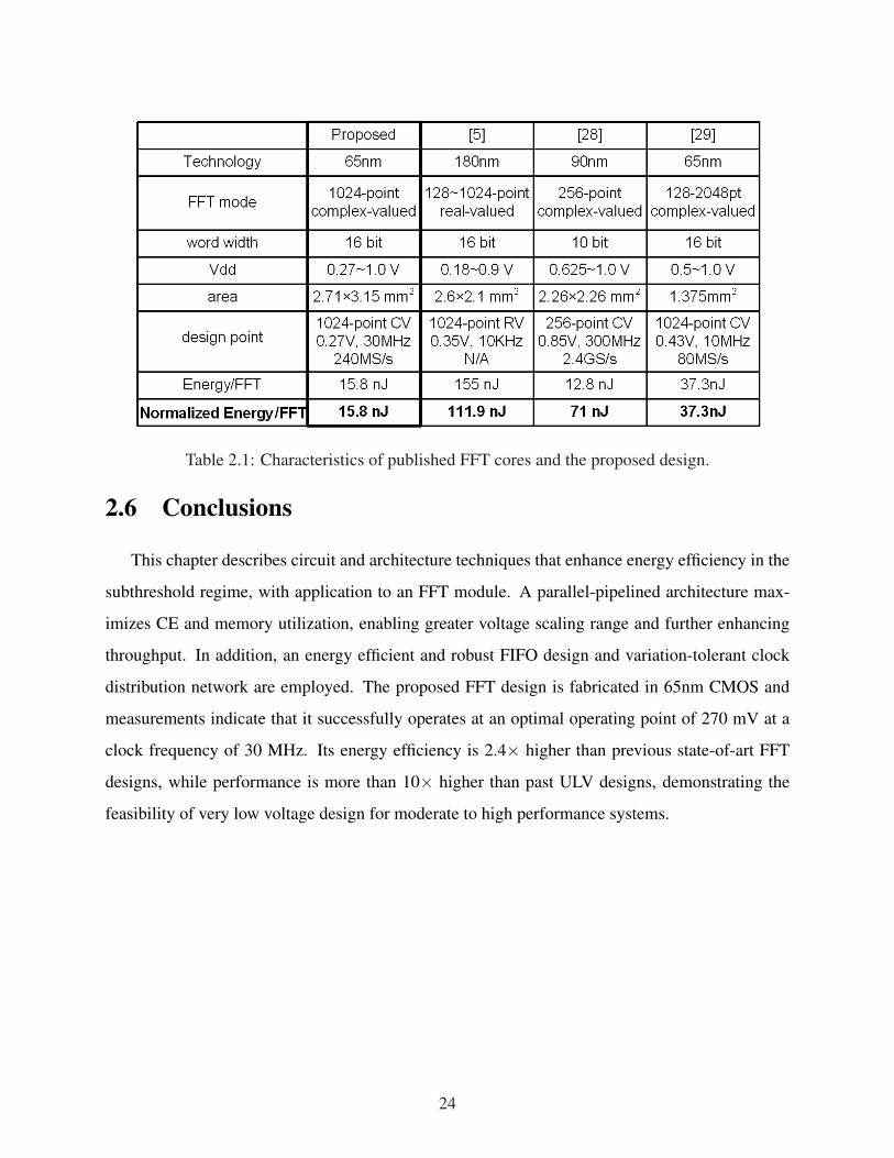
Table 2.1: Characteristics of published FFT cores and the proposed design.
2.6 Conclusions
This chapter describes circuit and architecture techniques that enhance energy efficiency in the
subthreshold regime, with application to an FFT module. A parallel-pipelined architecture max-
imizes CE and memory utilization, enabling greater voltage scaling range and further enhancing
throughput. In addition, an energy efficient and robust FIFO design and variation-tolerant clock
distribution network are employed. The proposed FFT design is fabricated in 65nm CMOS and
measurements indicate that it successfully operates at an optimal operating point of 270 mV at a
clock frequency of 30 MHz. Its energy efficiency is 2.4× higher than previous state-of-art FFT
designs, while performance is more than 10× higher than past ULV designs, demonstrating the
feasibility of very low voltage design for moderate to high performance systems.
24

CHAPTER 3
Design Methodology for Voltage Overscaled Ultra-Low Power
Systems
3.1 Introduction
Continuous technology scaling enables complicated DSP algorithms to be implemented in
highly energy-constrained systems such as wireless sensor nodes. Along with technology im-
provements, voltage scaling has also been applied in a wide range of applications to further reduce
power consumption. Although this effectively boosts energy efficiency by reducing dynamic en-
ergy, it also increases stage delay, translating to significant leakage energy per cycle in the near
and subthreshold regimes. Therefore a lower bound on energy per operation is reached in these
operating regimes [11][44].
However, the worst-case critical path in a design is not always activated and supply voltage can
be further scaled while maintaining fixed performance if the system can tolerate timing errors. This
enables improved energy efficiency beyond the lower bound described above via removal of the
timing correctness assumption. To reduce margins in conventional error-free systems, some cir-
cuit techniques [45] can detect and correct timing errors. While this allows for aggressive voltage
scaling, the energy overhead of error correction eventually exceeds energy savings from voltage
scaling beyond some error rate. On the other hand, some DSP systems have innate algorithmic
error-tolerance or can be modified to achieve error tolerance without significant quality degrada-
tion as shown in [15][46]. These types of systems show much larger benefit from VOS (voltage
25

overscaling) compared to error-free computing systems with additional error correction circuitry.
In voltage overscaled error-tolerant systems, it is critical to understand the tradeoff between
energy savings and quality degradation in order to estimate headroom during the design phase and
select an appropriate design point. Therefore an accurate timing error model for digital systems is a
key enabler to design using voltage-overscaling. One approach to building such a model is through
exhaustive search with simulation tools. However, the required time increases impractically as
the system grows. A preferred alternative would be a simple probabilistic timing error model that
provides reasonable accuracy, and makes the design of large DSP systems targeted at extreme
energy efficiency feasible.
In this chapter, a practical design framework using an analytical timing error distribution model
is proposed. Starting from the analysis of a simple ripple carry adder, a normally distributed error
model for more complex circuits is derived. The model fits reasonably well to typical circuit
building blocks using simulation and measurement results of pipelined Baugh-Wooley multipliers.
Then the proposed model is applied to an error-resilient K-best decoder to obtain an optimal design
point for peak energy efficiency.
3.2 Related Work
3.2.1 Error-tolerant DSP applications
The computation quality of many DSP systems can be measured as SNR performance. Gener-
ally such systems are allowed to incur a reasonably low SNR degradation (often less than 1dB) to
achieve a given power budget or performance target. In [47], the authors perform intensive simu-
lations of different adder types and investigate the benefit of VOS in a FIR filter. The work mainly
focuses on the average error magnitude without architectural modification to suppress timing er-
rors. However, error correction is not considered and performance degrades sharply as voltage
scales.
More advanced approaches that incorporate error correction schemes were proposed in [15] and
[46]. An estimator that is a simpler version of the main computation block produces approximate
calculation results, which are then compared with the result from the main block to detect timing
26

errors. If the difference exceeds a pre-decided limit, the estimator result is chosen and sent to the
next stage. The authors claim up to 71% power savings with coding gain loss of 0.8dB relative to
error-free systems including PVT variations.
3.2.2 Design approach for voltage overscaled systems
Design approaches to enhance or estimate the effect of VOS have been previously proposed.
Reference [48] suggests a design flow to redistribute slack for maximizing the amount of VOS. The
method is effective in improving VOS, but requires intensive simulations to determine the degree
of improvement. In [49] a similar flow is proposed with additional weight assignments including
a detailed analysis on adders and CORDIC processor.
In [50], the authors assume that the delay of a single gate follows the Gaussian distribution and
estimate error rate of a given circuit using simulation. They use clock skew scheduling based on the
importance of each signal to improve voltage scalability. Although this provides a simple design
approach for voltage overscaled systems, it may not be feasible to carefully control clock skew in
ultra-low power designs given that the corresponding low operating voltages lead to heightened
PVT variation. In addition, the approaches above use empirical models that do not directly extend
to other systems without significant recharacterization.
3.3 Error Analysis in Voltage Overscaled Systems
The conventional error analysis methods described above are based on extensive simulations.
They can reveal an error model underlying the circuit topology and enable prediction of the benefits
of voltage scaling. However, upon design modification (e.g., changing the pipeline stage assign-
ment and redistributing timing slacks), the analysis must be performed again with mostly different
variables, making it challenging to determine the optimal design point. To mitigate this exhaustive
search problem, this chapter proposes a simple timing error model that can be applied to general
complex circuits with acceptable accuracy to provide design guidance.
27

Figure 3.1: Critical path and an example activated path in a 32-bit ripple carry adder.
3.3.1 Ripple carry adder starting point
The adder is a basic element in typical DSP systems and even larger modules such as multipliers
are frequently implemented with multiple adders. By first finding an accurate error model for
adders, the model can be extended to the analysis of larger complicated modules. Here a ripple
carry adder is chosen as a testbench since it has a simple critical path and makes it possible to
understand the nature of timing errors and hence build an intuitive model.
The worst-case critical path of a ripple carry adder is well known to be the carry propagation
path from the LSB to the MSB, as shown in Fig. 3.1. For error-free computation, the pipeline
stage should be designed to accommodate this worst-case delay. However, the full critical path
is activated infrequently given the probability of appropriate input vectors. Using this, one can
calculate the probability of timing errors across the input vector space. Since the path from LSB to
MSB is the longest, it is assumed that the packet error rate can be approximated by the MSB error
rate. Then the probability that the length of the activated path culminating at the MSB is exactly N
in terms of the number of full adders is given by
pN = pN(1− p) (3.1)
where p is the probability that the carry input of the full adder propagates to the next stage.
Then the error rate is given by the probability that the length of the activated critical path is larger
than the clock period N, which is the sum of pk for all k>N. If p is 0.5 and the clock period is T,
then the probability ET that a timing error occurs is given by
ET =32
∑N=T/d f a
pN ≈ 0.5T/d f a (3.2)
28

Figure 3.2: Error rate of RCA from simulation and proposed equation.
where d f a is the delay of a single full adder. Fig. 3.2 shows the error rate of a ripple carry
adder from simulation in 65nm CMOS technology as well as estimated using Eq. 3.2. The results
confirm the model accuracy in predicting error rates.
While an accurate error model for the simple RCA can be easily found, an extendable prob-
abilistic model that can apply to larger systems is needed. As system size grows, there are more
critical and sub-critical paths in the module and the error pattern starts to behave more probabilis-
tically in contrast to the relatively deterministic model in Eq. 3.2. Given a system with N critical
paths following independent delay distributions, the error rate at the clock period T is given by
Esystem;T = 1−N
∏k=1
(1−Ek,T ) (3.3)
where Ek,T is the error rate of the kth critical path.
To simplify, it is assumed that all critical paths have distributions identical to Eq. 3.2 in order
to represent a complex system with multiple critical paths of the same delay. Then the CDF (Cu-
mulative Distribution Function) and the PDF (Probability Density Function) are obtained as shown
in Fig. 3.3. Rather than increasing continuously as the timing slack shrinks, the behavior of the
29
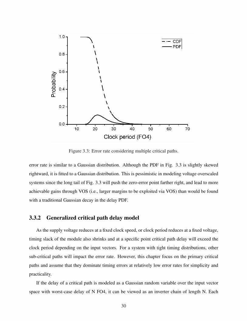
Figure 3.3: Error rate considering multiple critical paths.
error rate is similar to a Gaussian distribution. Although the PDF in Fig. 3.3 is slightly skewed
rightward, it is fitted to a Gaussian distribution. This is pessimistic in modeling voltage overscaled
systems since the long tail of Fig. 3.3 will push the zero-error point farther right, and lead to more
achievable gains through VOS (i.e., larger margins to be exploited via VOS) than would be found
with a traditional Gaussian decay in the delay PDF.
3.3.2 Generalized critical path delay model
As the supply voltage reduces at a fixed clock speed, or clock period reduces at a fixed voltage,
timing slack of the module also shrinks and at a specific point critical path delay will exceed the
clock period depending on the input vectors. For a system with tight timing distributions, other
sub-critical paths will impact the error rate. However, this chapter focus on the primary critical
paths and assume that they dominate timing errors at relatively low error rates for simplicity and
practicality.
If the delay of a critical path is modeled as a Gaussian random variable over the input vector
space with worst-case delay of N FO4, it can be viewed as an inverter chain of length N. Each
30

inverter delay also follows the Gaussian distribution with mean µ and standard deviation σ. There-
fore the delay of entire critical path becomes the sum of random variables as in
Dpath =N
∑k=1
Dinv,k ∼ N(Nµ,Nσ2) (3.4)
where Dpath and Dinv,k are the delays of the entire critical path and single inverter, respectively.
Then the timing error rate is the probability that Dpath exceeds a given timing constraint, which
can be calculated with the CDF of a normal distribution.
Although this simplified model trades off some accuracy compared to exhaustive search, it
greatly simplifies error rate prediction, making it easier to tailor the design a voltage overscaled
system. If the values of µ and σ are known, then distributions of the various pipeline stages and
modules in a large system are estimated with this simple equation. Furthermore, timing slack
redistribution or tuning of pipeline depth may be performed without costly iterative simulations.
3.3.3 Model verification with pipelined Baugh-Wooley multipliers
This section investigates the accuracy of the simple model described above in predicting error
rate behavior of larger digital modules. Since the multiplier is one of the key components in
DSP systems and is usually significantly larger than an adder, it is selected as a testbench. In
the subthreshold regime, exponentially increased stage delay contributes to large leakage energy
per operation and limits achievable energy efficiency. This leakage energy consumption can be
suppressed by pipelining (increasing overall circuit activity and making dynamic energy dominant
over leakage energy for a wider range of supply voltages) and pipelined multipliers may achieve
better energy efficiency than un-pipelined multipliers [21]. However, added pipeline registers incur
switching power overhead and there exists an optimal number of pipeline stages that gives the
lowest energy per operation. In this section, the proposed model is used to find the optimal pipeline
depth for a voltage-overscaled multiplier.
Pipelined Baugh-Wooley multipliers with various pipeline depths are implemented and Fig.
3.4 shows fabricated un-pipelined and 5-stage pipelined versions. These designs were fabricated
in 65nm CMOS technology as a testbench to compare the prediction model with simulation and
measurement results. To validate the proposed delay model, it should be determined whether the
31

Figure 3.4: Fabricated un-pipelined and 5-stage pipelined multipliers in 65nm.
Figure 3.5: Error rate quantile-clock period plot from measurements of the un-pipelined multiplier.
32

actual error rate distribution follows the Gaussian assumption. Measured error rate of un-pipelined
multiplier is shown in Fig. 3.5 and the plot indicates the linear relationship between clock period
and error rate quantile, therefore the proposed model reasonably reflects the behavior of error
probability.
Given an un-pipelined multiplier with critical path delay of N FO4 that follows the normal
distribution N(µ,σ2), a K-stage pipelined multiplier will have a critical path delay of N(µ′,σ′2)
with the relationships:
µ′ = µ/K,σ′ = σ/√
K (3.5)
based on the model in Eq. 3.5. In addition, pipelining may increase the number of first-order
critical paths, which this should be included in error rate calculations. Then the error rate of a
K-stage pipelined multiplier at a given clock period T is given by
Emult;k,T = 1−{F(T ;µ′,σ′2)}C (3.6)
where F is the CDF of a Gaussian distribution and C is the number of critical paths. For voltage
overscaled systems, the effect of voltage scaling translates to increased gate delay and T effectively
becomes shorter when normalized to FO4 delay at the new voltage. Therefore it is directly reflected
by T in this equation.
To measure the quality of the Gaussian-based prediction model, both un-pipelined and pipelined
multipliers with pipeline depths of 2, 4, and 5 stages are implemented. The exact values of µ and
σ for each multiplier are chosen by fitting Eq. 3.6 to simulation results as shown in Fig. 3.6. The
expected values of µ and σ can be calculated by using Eq. 3.5, where K is defined as the ratio
of worst-case critical path delays between the differing pipeline implementations, rather than the
number of pipeline stages to compensate for sequential overhead and stage delay mismatch. The
results from simulation and Eq. 3.5 are depicted in Fig. 3.7 showing that the proposed model
successfully predicts µ and σ with errors less than 8.4% and 15.5%, respectively.
Fig. 3.8 shows measurement results of un-pipelined and 5-stage pipelined multipliers along
with simulated values and model predictions. The proposed model accurately predicts the mea-
sured error rates. Since the model calculates the probabilistic delay over the input vector space,
33

Figure 3.6: Simulated and estimated error rates of various multiplier designs.
Figure 3.7: µ and σ from simulation and the proposed model.
34

Figure 3.8: Measurements of un-pipelined and 5-stage pipelined multipliers.
Figure 3.9: Energy consumption-error rate plot from simulation.
35

Figure 3.10: K-best decoder architecture.
there exists a lower limit of error probability. For example, if the worst-case critical path of a 16-bit
RCA is activated with only one set of input vectors, then the lowest possible error rate is 2−32. As
the multiplier is pipelined more deeply and includes more critical paths, the probability of critical
path activation increases significantly, raising the lower limit on error rate. In Fig. 3.8, the error
rate of the 5-stage pipelined multiplier drops very quickly above 300mV since the critical paths of
CSA trees are not activated and timing errors only occur in the carry skip adder with its slightly
longer critical path delay. At 305mV, both multipliers have zero error rates.
Fig. 3.8 also shows the margins for VOS with a maximum error rate tolerance of 0.1. As also
seen in Fig. 3.6, this margin reduces continuously for increasing pipeline depth. From this obser-
vation, the optimal number of pipeline stages in a voltage overscaled multiplier can be calculated.
Detailed analysis of the tradeoff between error rate and energy efficiency is given in Fig. 3.9. Al-
though a 4-stage pipelined multiplier is the most energy efficient at error-free operation, a 2-stage
pipelined multiplier shows better efficiency at error rates of 10−3 10−4 due to the sharper increase
in error rates in more heavily pipelined systems. Similarly, the proposed model can be applied to
other systems to determine an energy optimal design for a given error tolerance.
3.4 Case Study: Error-Resilient K-Best Decoder
For modern and next-generation communication standards, MIMO (Multiple-Input and Multiple-
Output) technique is a key feature. Although sphere decoding or other ML (Maximum Likelihood)-
like decoding schemes can achieve maximum decoding performance, the K-best decoder has been
proposed to mitigate fluctuating throughput and high hardware costs without significant SNR
degradation [51]. K-best decoding is based on the breadth-first search algorithm. It accumulates
the Euclidean distance from received symbols to candidate symbols and selects the fixed num-
36

Figure 3.11: Voltage overscaled CE assignment scheme.
ber of candidates with minimum distances at each search stage. The K-best decoder consists of
computational elements (CE) and sorters. The CE calculates the Euclidean distance to the most
promising child nodes of candidate lists from the previous stage and sends this information to the
sorters. The sorter then sorts the child nodes based on distance and builds a new K-best candidate
list. Fig. 3.10 depicts the K-best decoder architecture with received signal y, channel information
R, and output symbol s.
To avoid an iterative search for the most promising child node and increase performance, the
CE is modified to expand only n child nodes of each candidate node on the list simultaneously
using the best child node decision scheme in [52]. The K-best candidate list from the previous
stage is already sorted and the lower nodes on the list have lower probability to survive until the
last stage since they have relatively larger distances than the upper nodes on the list. This implies
that even if an error occurs during node expansion of lower nodes, it may not noticeably degrade
the overall decoding performance. Therefore, if two separate CEs are used for the upper half and
lower half nodes on the list one can obtain error-tolerance by employing a voltage overscaled CE
to the latter case as shown in Fig. 3.11. A simple circuit-based timing error detection only scheme,
such as in [44], can detect errors and set the calculated distance to infinity to remove erroneous
results, eliminating overhead from error-correction modules such as in [45]. SNR degradation due
to voltage overscaled CE in a practical K-best decoder design with K=10 and l=3 is described
in Fig. 3.12. This plot indicates that the proposed error-resilient K-best decoder can tolerate
a calculation error rate of CE module as high as 0.3 with SNR degradation less than 0.4dB at
BER=10−3.
The described CE module was synthesized using 65nm CMOS technology and the detailed
37

Figure 3.12: SNR-BER plot for different error rates.
architecture with critical paths is shown in Fig. 3.13. In this figure, a critical path consists of two
adders and a multiplier in series and can be pipelined more deeply to improve performance. Fig.
3.14 shows two pipelined critical paths with different number of stages, and the remaining part
of the CE is also pipelined accordingly to match the performance in both cases. As shown in the
pipelined multiplier analysis of the previous section, a 3-stage pipelined design allows for a shorter
stage delay and lower leakage energy. At the same time, the pipeline registers incur sequential
energy overhead and the error rate of entire module increases much faster due to reduced critical
path delay in Eq. 3.6. The exact error rate at a given voltage can be calculated with the prediction
model of the previous section. The critical path delay of a 1-stage CE (un-pipelined) is expressed
as the sum of three random variables, two adder delays and one multiplier delay, and that of 3-stage
pipelined one is dominated by the un-pipelined multiplier since its error rate increases much faster
than the adder. Fig. 3.15 shows the calculated error rate increase. In Fig. 3.16, the relationship
between energy consumption and CE error rate for two different pipeline depths is shown. At the
error-free operating point where Vdd=300mV, a more deeply pipelined CE consumes less energy.
However, as the voltage scales the error rate of the 3-stage pipeline CE increases rapidly and the
38

Figure 3.13: Detailed CE architecture.
39

Figure 3.14: Two different pipeline stage assignments for critical path.
Figure 3.15: Error rate of voltage-overscaled CEs.
40

Figure 3.16: Energy-error rate tradeoffs of CE for different pipeline depths.
energy per operation becomes the same for the two cases at an error rate of 10−1. For the given
error tolerance of 0.3, the un-pipelined CE consumes 1.4% less energy per operation. In addition,
since the un-pipelined design has a longer stage delay, it may achieve greater tolerance to PVT
variations thanks to averaging effects, making it a better design choice for subthreshold operation.
The total energy savings from VOS in this design is 22.5% at 12.1% VOS, as shown in Fig. 3.16.
3.5 Conclusions
This chapter investigated the effect of voltage overscaling and proposed a framework for volt-
age overscaled DSP system design in the ultra-low voltage regime. Starting from simple rip-
ple carry adder simulations, it is found that the error rate can be modeled using probabilistic
critical path delays and subsequently proposed a generalized Gaussian distributed critical path
delay model. This model enables rapid design decisions with reasonable accuracy, and was con-
firmed with silicon measurements and simulations of pipelined Baugh-Wooley multipliers in 65nm
CMOS. An error-tolerant K-best decoder architecture that can tolerate CE error rate as high as
41

0.3 with SNR degradation less than 0.4dB was also proposed as a case study. By applying the
proposed framework, the optimal pipeline scheme for higher energy-efficient operation of CE in
error-resilient K-best decoder is achieved, which provides 22.5% saving using voltage overscaling.
42

CHAPTER 4
Energy-Optimized Feature Extraction Accelerator
4.1 Introduction
In the last decade, computer vision has been widely applied to many different fields. In medical
imaging such as MRI or CT, images are analyzed using computer vision techniques to realize fully
or partially automatic diagnosis [53][54]. Recent advanced surveillance camera systems not only
record video, but also provide functions including facial recognition and motion detection [55].
Automobile manufacturers incorporate various cameras on vehicles and analyze their external en-
vironment to improve driving safety or achieve self-driving functionality [56]. Although computer
vision algorithms typically require substantial computing power, conventional applications such as
those mentioned above have rather large power budgets and hence supporting these computational
requirements has been feasible.
Recently, mobile battery-powered systems such as cellular phones, micro-robots and millimeter-
sized sensor nodes have gained significant attention. Due to technology scaling and the develop-
ment of new low-power techniques, these application areas continue to flourish, incorporating
more functionality with time [2][57]. Computer vision techniques can add significant value to
these classes of systems, providing various useful features such as object recognition in phones or
navigation and surveillance in micro-robots. However, the tight power constraints of these systems
prevent practical implementations of computer vision algorithms. This chapter therefore seeks to
significantly reduce hardware cost and power consumption associated with such algorithms.
This chapter describes a highly energy-efficient feature extraction accelerator design for visual
43

Figure 4.1: An example of object recognition using extracted features [58].
navigation of micro-autonomous vehicles. A modified feature extraction algorithm that improves
energy efficiency while maintaining feature extraction quality is first proposed. Then architectural
and circuit techniques including a robust low-power FIFO for subthreshold operation are applied
to reduce power consumption further.
4.2 Proposed Visual Feature Extraction Algorithm
4.2.1 Visual feature extraction
Visual feature extraction is a key step in many computer vision algorithms. Essentially it ex-
tracts useful information from a visual source such as a n image, and this information can be used in
a variety of applications including object recognition and pose estimation. Fig. 4.1 shows an exam-
ple of the widely-used SIFT (scale-invariant feature transform) algorithm [58]. Feature extraction
is performed on the original image (left), and small rectangles depict extracted features with differ-
ent scales and orientations. These are then compared to features already stored in the database and
finally some objects are recognized (right). Generally feature extraction should provide scale and
rotation invariance for reliable extraction under different circumstances or viewpoints, as shown in
Fig. 4.2.
SURF (Speeded-Up Robust Features) is a well-known variation of the SIFT algorithm. The
authors of [59] claim it achieves identical or even superior extraction quality while reducing com-
putational cost significantly, making it attractive for low-power applications. SURF consists of two
44

Figure 4.2: Two key constraints of feature extraction algorithms: (a) rotation and (b) scale invari-ance.
Figure 4.3: Original feature vector generation process consisting of (a) orientation assignment and(b) feature vector generation [59].
45

distinct stages: detection and description. In the detection stage, an input image is first processed
with multiple filters at different scales. Filter responses calculated simultaneously at different
scales provide the scale invariance property. The algorithm then searches for interest points (lo-
cal maxima) in 3-D scale-location pyramids. Although local maxima points can be extracted using
simple digital comparators, the actual maxima point can reside somewhere between adjacent pixels
and matrix-based equations are used to interpolate the maxima point in 3-D space. The description
stage is responsible for describing each interest point and generating a corresponding final feature
vector . For rotation invariance, the orientation of each interest point must be determined first. It
collects filter responses around it and searches for an angle which has largest filter responses using
rotating sampling window as depicted in Fig. 4.3(a). After choosing orientation, a rectangular
sampling region is rotated by that angle and filter responses are again collected in that region (Fig.
4.3(b)). This guarantees that collected responses around each interest point remain unchanged in
images rotated by any angle. The sampling region is divided into small rectangles and a summation
of sampling responses in each sub-region constitutes each dimension of the feature vector. Finally,
this vector is normalized such that vectors extracted from different scale images have identical
magnitude.
4.2.2 Proposed hardware-oriented feature extraction algorithm
The SURF algorithm is applied to the design target, a MAV (micro air vehicle) with visual
navigation shown in Fig. 4.4, where feature extraction is a key function and a dominant power
consumer . The MAV is designed to fly and navigate in indoor environments using various sensors
to recognize obstacles and a camera for location search. Fig. 4.5 provides an overview of the
visual navigation system [60]. First, an on-board camera captures 30 fps VGA video , which is fed
into the proposed feature extraction accelerator. The feature extraction accelerator then extracts 64-
dimensional SURF features that are compared to location database storing features from previously
visited locations. If any match is found, it can be concluded that the test vehicle has returned to a
location visited before and a loop closure is declared. Finally, this loop closure information is used
in an algorithm called SLAM (Simultaneous Localization and Mapping). SLAM continuously
monitors the environment to determine current location and generate a map. Physical sensors such
46

Figure 4.4: A target application of MAV with visual navigation.
Figure 4.5: An overview of the visual navigation algorithm flow.
47

as gyroscopes, accelerometers, and lasers provide primary information on vehicle movements,
but small errors accumulate over time and cause localization to fail at some point. Loop closure
information from previous steps is used in this SLAM algorithm to compensate for these errors. In
this class of system, feature extraction is one of the most computationally expensive steps, and this
work therefore focuses on the design of a corresponding accelerator.
Since MAVs can move rapidly, they must perform both accurate and fast feature extraction. In
addition, location monitoring should be done continuously, however a direct implementation on an
X86 embedded processor consumes more than 1W while processing only 1 fps (frame per second).
Related work on custom-designed hardware for similar applications also report > 50mW power
consumption [61][62][63][64] for processing partial images based on ROIs (Regions of Interest).
However, this system has a tight power budget of 10mW for digital processing due to a minimum
required operation time without recharging. This power budget includes feature extraction as well
as other functions such as feature mapping and navigation.
One widely used technique to reduce power consumption in image processing is the extraction
of ROIs. A low-cost pre-processing stage is inserted before the actual feature extraction step to
search for small regions believed to have meaningful information or targeted objects. An input im-
age is divided into many smaller tiles and only a subset of these are chosen for further processing.
Although this can significantly reduce power consumption, the performance of the pre-processing
algorithm dictates the overall quality of feature extraction. Furthermore, the target application
compares each captured image on a scenery basis (not individual objects), necessitating feature
extraction from the entire frame.
To achieve low power while performing full-frame feature extraction, the original SURF al-
gorithm is optimized with the goal of an energy-efficient hardware implementation without using
an ROI-based approach. First, the detector uses a single-octave scale space (Fig. 4.6(a)). Since
the target resolution is 640×480, only a small portion of extracted features reside in the second
or higher scale pyramids. It chooses the first octave among them but employs an additional filter
with size 33 to compensate for lost features. The resulting algorithm extracts more than 99% of
originally extracted features while reducing filter power consumption by 38%. After local maxima
detection, the exact original location of the maxima is typically be calculated using matrix-based
arithmetic operations. Instead, a fast localization technique is used for interpolation as described
48

Figure 4.6: Proposed (a) single-octave scale space; and (b) fast localization techniques for detectoroptimization.
Figure 4.7: Proposed circular-shaped sampling region approach.
in Fig. 4.6(b).
In the description stage, a large and variable number of interest points marked by the detector
must be processed. Previously a multi-core architecture has been proposed to deal with the vari-
able throughput of this step [61][62][63]. As discussed in the previous section, for each interest
point two separate filter response sampling steps are required for orientation assignment and actual
description, respectively. In other words, the complete filter responses around each interest point
should be transferred to a description core responsible for describing that point. These responses
also have to be stored temporarily in data memory within each core for later steps. This necessitates
a large buffer in each description core, which incurs a large area and power overhead .
Instead, the proposed design has a circular-shaped sampling region that unifies orientation
49

Figure 4.8: Unified description process consists of (a) filter response calculation; (b) summationin circular-shaped sampling region; and (c) reordering and normalization of feature vector.
assignment and description into one step as shown in Fig. 4.7. The authors in [65] compare polar
grid samplings and a rectangular grid, shedding light on the possibility of using a rotation invariant
sampling region. However, to avoid two separate sampling methods and use all available sampling
points within a circle, the proposed sampling region is still based on the original rectangular grid.
Instead, it is divided into 32 subsections and a vector representing an interest point is generated
based on the summation of filter responses in each subsection. Since the number of points in
even- and odd-numbered subsections are different, the kth angle is composed of filter responses
gathered in both kth and (k+1)th subsections such that all angles have the same number of sampling
points. The interest point orientation can be easily determined by the subsection with the largest
summation value.
Since the shape and coverage of a circular-shaped sampling region do not change when rotated
by the assigned orientation, filter responses do not need to be re-collected for actual description.
Furthermore, by restricting orientation angles to discrete values represented by each subsection,
final feature vectors can be generated by simply re-ordering vector dimensions as seen in Fig. 4.8.
Although this technique provides only discrete step rotation, the use of 32 subsections translates
to a small rotation step of only 11.25. As a result, each description processing element does not
have to store entire filter responses and instead just accumulates them into 32-dimensional vectors
in real time, reducing memory requirements in each core by 89% and entire core area by 80%.
This technique also enables other hardware design simplifications that are discussed in detail in
the Section 4.3.
The proposed modified SURF algorithm was tested using actual videos captured by a robotic
50

Figure 4.9: (a) Rotation; and (b) scale invariance performance comparisons.
test vehicle. Fig. 4.9 demonstrates the measured feature extraction quality, defined by the ratio
of the number of correctly matched features to the number of all matched features between orig-
inal and re-scaled or rotated images. These plots confirm that the scale and rotation invariance
performance of the proposed and original SURF algorithms are very similar.
4.3 Energy-Efficient Hardware Architecture
4.3.1 Accelerator architecture
Voltage scaling is a widely used and effective power-saving technique [24][9][19], but it incurs
large performance penalties that are unacceptable in high throughput systems. Feature extraction
algorithms are generally computationally expensive and SIFT/SURF algorithms require through-
put on the order of GOPS or higher. In addition, the number of features in each frame varies
widely and hence peak performance requirements can be much higher than typical performance.
Therefore, a feature extraction accelerator must be designed carefully to effectively incorporate
aggressive voltage scaling while also meeting high performance requirements.
Fig. 4.10 shows the overall architecture of the proposed accelerator design. To deal with the
low clock frequencies associated with deep voltage scaling, the accelerator is uniquely designed
to take only one pixel of input image per cycle at the low speed of 27MHz. In addition, the entire
51

Figure 4.10: Proposed feature extraction processor architecture.
Figure 4.11: Overlapped image subsections are processed successively to allow for proper featureextraction at boundaries.
52

accelerator operates at the same clock frequency, resulting in a matched-throughput system. A
640×480 8-bit grayscale input image is divided into 11 subsections, as shown in Fig. 4.11, and
they are processed successively. Subsections are partially overlapped to allow the accelerator to
extract features from the entire area including borders between subsections.
Each subsection has 640×124 pixels. In each cycle, only one pixel of the input image is fed into
the proposed accelerator. It is first integrated in 2-D and Gaussian box filters with different scales
are applied. Filter responses form a 3-D scale-location space and a local maxima detector searches
for the interest points in this space. Finally, an interpolator determines the exact location of maxima
using the proposed simplified maxima detection technique. While the detector is searching for
interest points, the input image must be delayed temporarily. Therefore, the input image is delayed
by a 7067-entry FIFO at the input stage of descriptor shown in Fig. 4.10. Then it is integrated in 2-
D in the same way as in the detection stage. Although the input image is integrated identically in the
detector and descriptor, the use of separate integrators actually reduces silicon area by minimizing
FIFO size. Since the original 8-bit input image becomes 18-bit after integration due to larger
dynamic range, FIFO area is reduced by 95,000µm2 (56%) while overhead from the additional
integrator is only 9,700µm2.
The integrated image goes through Haar wavelet filters in different scales, which provides the
necessary filter responses for feature description. While the interest point information from the
detector is passed to descriptor processing elements in real time, one of the idle processing ele-
ments is assigned to it. Each processing element captures the Haar wavelet filter responses around
each point and generates feature vectors. The proposed design uses 40 processing elements in
total, and they are power-gated when not in use. The number of processing elements is chosen to
provide more than 2 margin compared to the maximum number of features being extracted simul-
taneously at one location in actual test images. Finally, a post processor reorders, normalizes, and
rotates generated feature vectors and produces the final output. Additional hardware techniques are
applied to further optimize each component, and these will be described in the following sections.
Reference [66] presents an early effort to adopt a similar dataflow and architecture. How-
ever, it is not fully matched-throughput system and remains partially based on the use of reconfig-
urable cores, which requires > 3× faster clock frequency for the same video throughput (increasing
power). In addition, a large buffer memory of 2.8Mb (compared to 56kb FIFO for delaying the
53

Figure 4.12: Image summation in a rectangular region implemented with 3 arithmetic operationson a 2-D integrated image.
Figure 4.13: Image summation calculators based on (a) a single datapath with memory and (b)multiple arithmetic units with different delay elements.
image in the proposed design) is required before the descriptor due to multi-stage description, and
peak performance is limited to 890 interest points per frame.
4.3.2 Parallelized filters and arithmetic blocks
Two different types of filters are used in the detector and descriptor, but their operation is
very similar and is based on simple arithmetic operations on the integrated image. Both Gaussian
box filters and Haar wavelet filters are based on the summation of an image, which can be easily
achieved by 2-D integrated image and simple arithmetic operations such as addition and subtraction
as shown in Fig. 4.12. In conventional multi-core architectures, this can be calculated using a single
54

Figure 4.14: Unrolled 2-D image integrator architecture.
arithmetic unit and processing one (or a few using a SIMD architecture) set of data in each cycle
(Fig. 4.13(a)). However, the entire image must be stored in a large memory and power overhead is
incurred in accessing this large memory every cycle. In addition, multiple operations are required
to obtain filter responses at one point and, therefore, the system must operate at a much higher
clock frequency, limiting aggressive voltage scaling. Although each summation over a rectangular
region requires only 4 data read and 3 arithmetic operations, the current approaches still consume
significant power when applied over an entire frame.
However, the proposed design has a fully unrolled and parallelized architecture for those filters
as depicted in Fig. 4.13(b). First, the input image is delayed by differing numbers of cycles using
different size FIFOs. As the input image continues to be processed, images with varying delays
appear at the FIFO outputs and they are used for filter response calculation at this point. Once all
FIFOs are completely filled with data, 3 arithmetic operations can be performed simultaneously
using a 3 lower clock frequency. This architecture allows for a single clock domain over the entire
accelerator and provides greater headroom for voltage scaling. In addition, each cycle data is
generated by relatively small FIFOs instead of a large memory, which reduces energy consumed in
data readout as well. Different size filters can be easily implemented using the same architecture
with adjusted delays.
Similarly, the 2-D image integrator can be implemented using only two adders and one 124-
entry FIFO, which produces one pixel of the integrated image per cycle in real-time (Fig. 4.14). A
3-D local maxima detector applied after the Gaussian box filters searches for local maxima in the
333 location-scale space. A total of 26 subtractions must be calculated in each cycle to determine
if a given point is larger than all neighboring points. However, the amount of computation can be
reduced significantly by reusing previous results. In each cycle, the lower 3 pixels of each scale
55

Figure 4.15: (a) Original and (b) proposed local maxima detection schemes. In (b), maximumpoint of each row is already stored and only one comparison per row is required.
are processed and the location of the maximum value among them is attached to the lower middle
pixel as an additional 2 bits. Each target point can then be compared to only 8 pixels (maxima of
each row) rather than 26 (Fig. 4.15), reducing the number of comparisons by 69%.
4.3.3 Single stream descriptor
Interest points extracted by the detector are continuously passed to the descriptor with each
point assigned to an idle processing element (PE). Based on responses of Haar wavelet filters, the
set of PEs must simultaneously process a large number of interest points depending on the input
image. Therefore, the descriptor must offer high peak performance while maintaining low power
consumption. This is handled through the use of many PEs, however this incurs high hardware
cost, particularly for data memory used to temporarily store filter responses around an interest
point. A conventional design uses a multi-core architecture as shown in Fig. 4.16(a). An inde-
pendent controller manages filter responses stored in a large central data memory, and the entire
sampling region around an interest point should be passed to a PE once the controller makes a PE
assignment. When the number of interest points is high, significant data is transferred through a
shared data bus, which requires a high-speed data bus operating at a high clock frequency [63].
Furthermore, overlapping regions sent to multiple PEs incur further overhead. After each PE re-
ceives sampling responses and stores them in local memory, it calculates feature vectors through
orientation assignment and the actual description step.
However, the proposed circular-shaped sampling region discussed in Section II.B unifies these
56

Figure 4.16: (a) Conventional multi-core architecture where each core communicates through ashared data bus independently. (b) Proposed architecture where a single response flows continu-ously through shared data bus and each core reads in only its required blocks.
57

two steps while removing the need for storing responses in local memory. This algorithm-architecture
co-optimization enables the proposed single stream descriptor in Fig. 4.16(b). In this architecture,
filter responses continuously flow through a shared data channel at a fixed low speed such that all
processing elements see the same data stream. Since interest points are assigned in advance, PEs
can easily identify the proper filter responses and capture data from the channel at the appropriate
time interval. Since entire filter responses are transferred through a shared data channel (regard-
less of the number of interest points), this channel can be realized with a fixed-throughput low
speed data bus, which allows lower power consumption with more aggressive voltage scaling. In
addition, this removes redundant data transmission for overlapped sampling regions, eliminating
unnecessary switching.
4.4 Latch-based Low-Power and Robust FIFO Design
The proposed accelerator architecture requires a large number of delay elements across all
sub-blocks. In particular, the 7067-entry FIFO at the input stage of the descriptor can consume
appreciable leakage and switching power, and both the Gaussian box filters and Haar wavelet
filters have many smaller FIFO blocks. It is therefore critical to choose a low-power FIFO block
that also offers robust behavior at near- or sub-threshold regime to facilitate aggressive voltage
scaling. This last requirement is challenging as there are several known problems in low-voltage
memory design.
First, very low on-off current ratios significantly degrade read and write margins, impeding
robust operation. Second, the impact of process variation at low voltage is magnified, causing
problems for large memory arrays where any single storage element could fail. Conventionally,
FIFOs are implemented with shift registers or 6T SRAM and a cyclic address generator [36][37].
SRAM is an attractive solution in the super-threshold regime due to its small area and low power
consumption. However, under aggressive voltage scaling its operating margins nearly disappear
with common failures below some Vcc,min value. Furthermore, SRAM bitcells suffers from large
variability due to small device sizes and read/write tradeoff and their relatively slow access time can
become a bottleneck at the system level in throughput-constrained applications. Robustness issues
can be overcome by adding more transistors (e.g., 8T or 10T), at the cost of area and power, while
58

slow access speeds remain [67]. On the other hand, shift registers are both very fast and robust
even at very low operating voltages. However, the density is several times worse than SRAM since
each storage cell consists of 2 latches. Master and slave latches switch every cycle and, therefore,
a shift register approach also consumes much higher switching power, exacerbated by the need to
propagate data in every cycle.
To overcome these issues in conventional FIFO designs, a new FIFO architecture based on
latches is proposed. The approach starts with a conventional shift register and replaces all storage
cells with latches; hence this approach is called shift-latch. It is impossible to move all data
simultaneously since latches are level-sensitive such that enabling all latches would lead to the
entire path becoming transparent. However, data can be propagated using a one-hot encoded enable
signal that moves in the opposite direction each cycle, as depicted in Fig. 4.17. Initially only the
4th latch is enabled and the value from the previous latch is written into this latch. As a result,
both the 3rd and 4th latches now have identical values with the 3rd latch becoming a redundant
cell called a bubble. In the next cycle, the enable signal is asserted at a location one stage earlier,
i.e., the 3rd latch is enabled in Fig. 4.17. This latch then accepts data from the 2nd latch, which
then becomes the bubble. In the following cycle, enable signal is staggered again and the 2nd latch
is enabled. As a result, data moves forward and the bubble moves backward again. Finally, the 1st
latch is enabled and input data is written to it. At the same time, data stored in the last latch is read
out through the output port and it becomes the bubble.
After N cycles all data values have propagated forward by one entry and one output is produced
from the last latch, completing one period. After N-1 periods, the value initially stored in the first
latch is shifted to the last latch and can be passed to a readout circuit. Therefore, this can be
viewed as a single FIFO lane with N(N-1) total FIFO delay and throughput of one output per
N cycles. Hence, a conventional one output per cycle FIFO is built by arranging N identical
lanes in parallel and connecting their enable signals diagonally (Fig. 4.18). In each cycle, exactly
one output is generated from different FIFOs and a conventional 1 output per cycle throughput
can be obtained by adding additional readout circuitry to choose the appropriate output among N
FIFO lanes. Fig. 4.19 shows an example of an 840-entry FIFO based on the proposed shift-latch
FIFO architecture. A cyclic address generator automatically generates the one-hot encoded enable
signals shared across all lanes. In the final design, each lane is activated only every other cycle
59

Figure 4.17: Proposed single-lane shift latch propagating data and a bubble in opposite directionsat each cycle.
60

Figure 4.18: A one-output-per-cycle FIFO consisting of N lanes and shared readout circuitry.
Figure 4.19: An 8-bit 840-entry FIFO based on the proposed shift-latch architecture.
61
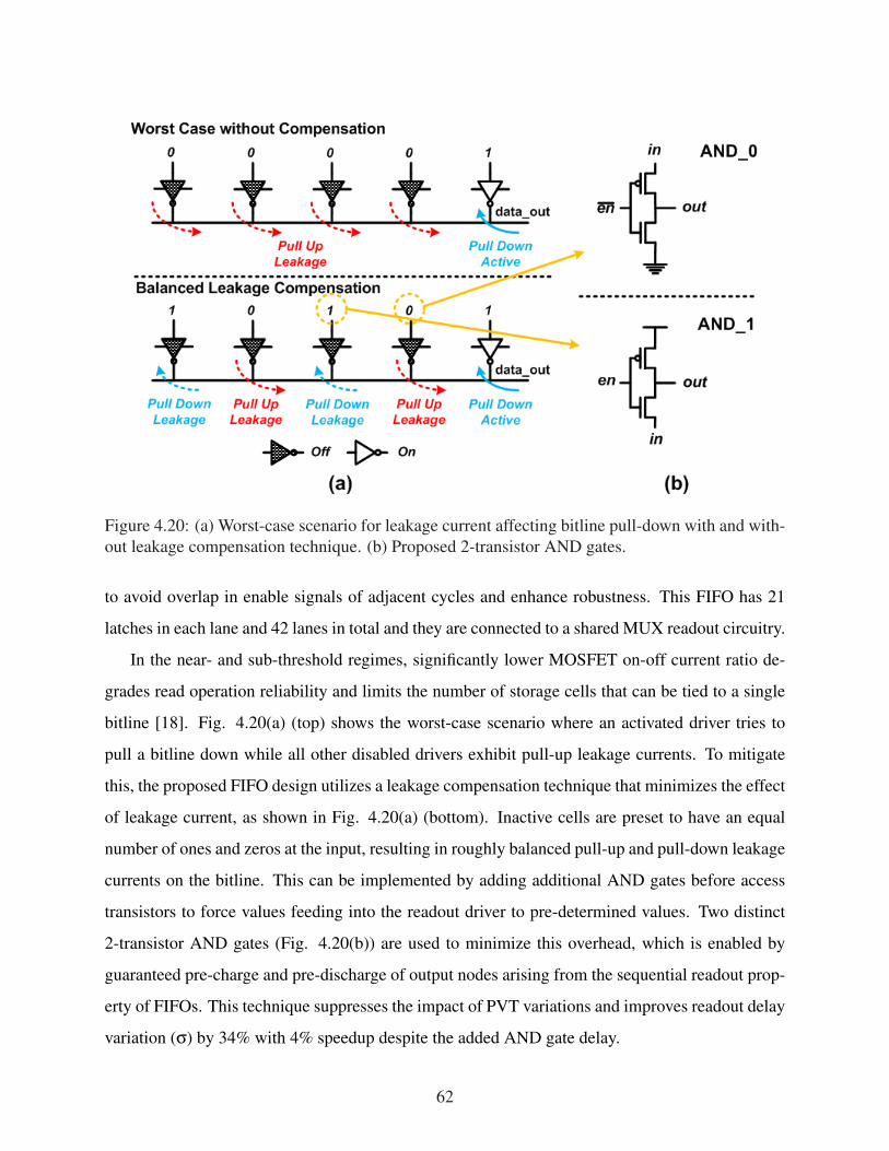
Figure 4.20: (a) Worst-case scenario for leakage current affecting bitline pull-down with and with-out leakage compensation technique. (b) Proposed 2-transistor AND gates.
to avoid overlap in enable signals of adjacent cycles and enhance robustness. This FIFO has 21
latches in each lane and 42 lanes in total and they are connected to a shared MUX readout circuitry.
In the near- and sub-threshold regimes, significantly lower MOSFET on-off current ratio de-
grades read operation reliability and limits the number of storage cells that can be tied to a single
bitline [18]. Fig. 4.20(a) (top) shows the worst-case scenario where an activated driver tries to
pull a bitline down while all other disabled drivers exhibit pull-up leakage currents. To mitigate
this, the proposed FIFO design utilizes a leakage compensation technique that minimizes the effect
of leakage current, as shown in Fig. 4.20(a) (bottom). Inactive cells are preset to have an equal
number of ones and zeros at the input, resulting in roughly balanced pull-up and pull-down leakage
currents on the bitline. This can be implemented by adding additional AND gates before access
transistors to force values feeding into the readout driver to pre-determined values. Two distinct
2-transistor AND gates (Fig. 4.20(b)) are used to minimize this overhead, which is enabled by
guaranteed pre-charge and pre-discharge of output nodes arising from the sequential readout prop-
erty of FIFOs. This technique suppresses the impact of PVT variations and improves readout delay
variation (σ) by 34% with 4% speedup despite the added AND gate delay.
62

Figure 4.21: Simulated (a) delay, area, and (b) energy consumption of baseline and proposed FIFOdesigns as a function of FIFO size.
Figure 4.22: Simulated energy savings in each component of a 1k-entry FIFO.
63

Figure 4.23: A microphotograph of the fabricated feature extraction accelerator and summarytable.
The proposed FIFO design was simulated and compared against prior work in low power
queues. The baseline design is a latch-based memory with a logic-based readout [21], represent-
ing one of the most energy efficient and robust designs at low voltages. It uses a cyclic address
generator and each storage cell is accessed through a logic-based readout path for fast and robust
readout. Fig. 4.21 provides simulation results that show the proposed shift-latch FIFO improves
readout delay and energy efficiency with smaller area compared to the baseline. For a 1k-entry
FIFO, the proposed design is 37% faster, 49% smaller, and consumes 62% less energy due to en-
ergy savings from shared address generator and readout circuitry. Fig. 4.22 shows detailed energy
savings in each component. Although more energy is consumed in storage cells because of shifting
data, energy savings from read and write circuitry dominate due to the slow logarithmic increase
of interface size for the proposed shift-latch FIFO.
64

Figure 4.24: Measurement results across different operating voltages.
4.5 Measurement Results
A feature extraction accelerator based on the proposed hardware and algorithm techniques is
fabricated in 28nm LP CMOS technology. Fig. 4.23 shows a microphotograph of the fabricated
design along with a summary table. It operates at the design point of 470mV with a clock speed
of 27MHz to process 30fps VGA video input. While continuously processing input video, the
accelerator consumes only 2.7mW with 149.3 GOPS performance, yielding a 55.3 TOPS/W energy
efficiency. Fig. 4.24 shows measurement results over a range operating voltages. This design can
operate down to 280mV, which represents the deep sub-threshold regime in this process, largely
due to robust FIFO design and careful standard cell selections. As voltage scales down, energy
efficiency starts to decrease at some point due to dominating leakage power and increasing cycle
time [9]. A peak efficiency of 67.2 TOPS/W is obtained at 375mV. The accelerator design can
process 4 fps at this operating point.
Fig. 4.25 presents a sample image from a camera on the robotic test vehicle, along with 1421
features extracted using the fabricated accelerator. Detected points near frame edges have sampling
regions overlapped with image borders and they are ignored for reliable extraction in this case. A
65

Figure 4.25: A sample image marked with 1421 extracted features from measurements.
Table 4.1: Comparisons of prior works and proposed design.
part of the image in the red box has clear parallel patterns and extracted features in this region have
very similar orientations, confirming proper feature extraction operation.
Table 4.1 provides comparisons between this work and recent prior works. The proposed ac-
celerator is targeted solely for feature extraction and extracts features from the entire frame in
contrast to other ROI-based designs. Although it was designed for VGA input video, the proposed
accelerator architecture does not vary with video size and it can be adjusted to process 1280×720
HD video with 81MHz clock frequency and 12mW power consumption at 600mV. For compari-
son, energy efficiency was scaled with respect to operating voltage and technology, and OPS/W
was used for comparison against other works with different functionalities. The proposed design
66

achieves 3.5× better energy efficiency over prior work.
4.6 Conclusions
This chapter proposed various hardware and algorithm techniques to realize a highly energy-
efficient feature extraction accelerator. Hardware-oriented algorithm optimizations reduce hard-
ware cost (e.g., area and power consumption) significantly while maintaining extraction quality.
The proposed accelerator architecture is focused on maximizing the benefits of deep voltage scal-
ing while meeting high throughput requirements. A new shift-latch FIFO architecture provides a
practical and efficient solution in the near- and sub-threshold regimes. A feature extraction acceler-
ator using these techniques is fabricated in 28nm LP CMOS technology and measurement results
confirm that it processes 30fps VGA video at supply voltages as low as 470mV at a low clock
speed of 27MHz. Overall, the design provides 3.5× higher energy efficiency than prior state-of-art
and offers full-frame feature extraction.
67
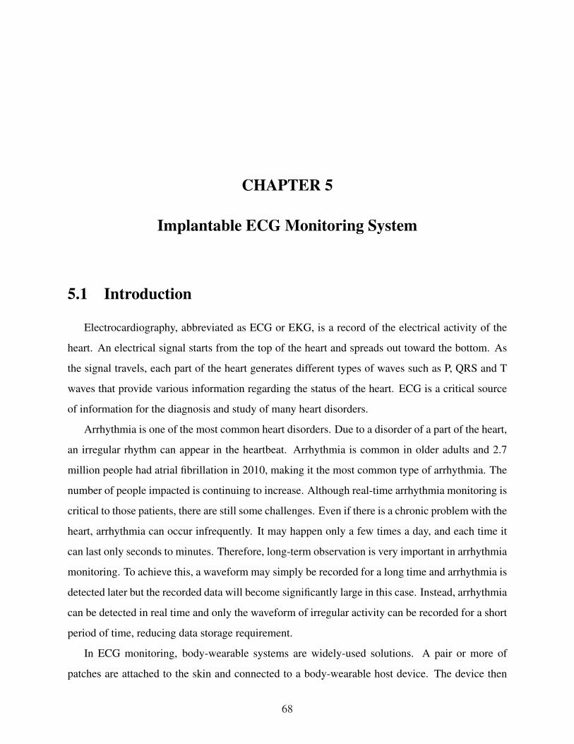
CHAPTER 5
Implantable ECG Monitoring System
5.1 Introduction
Electrocardiography, abbreviated as ECG or EKG, is a record of the electrical activity of the
heart. An electrical signal starts from the top of the heart and spreads out toward the bottom. As
the signal travels, each part of the heart generates different types of waves such as P, QRS and T
waves that provide various information regarding the status of the heart. ECG is a critical source
of information for the diagnosis and study of many heart disorders.
Arrhythmia is one of the most common heart disorders. Due to a disorder of a part of the heart,
an irregular rhythm can appear in the heartbeat. Arrhythmia is common in older adults and 2.7
million people had atrial fibrillation in 2010, making it the most common type of arrhythmia. The
number of people impacted is continuing to increase. Although real-time arrhythmia monitoring is
critical to those patients, there are still some challenges. Even if there is a chronic problem with the
heart, arrhythmia can occur infrequently. It may happen only a few times a day, and each time it
can last only seconds to minutes. Therefore, long-term observation is very important in arrhythmia
monitoring. To achieve this, a waveform may simply be recorded for a long time and arrhythmia is
detected later but the recorded data will become significantly large in this case. Instead, arrhythmia
can be detected in real time and only the waveform of irregular activity can be recorded for a short
period of time, reducing data storage requirement.
In ECG monitoring, body-wearable systems are widely-used solutions. A pair or more of
patches are attached to the skin and connected to a body-wearable host device. The device then
68

monitors ECG continuously and stores the waveform if necessary while typically being powered
by a battery. It is relatively easy to implement such a system due to relaxed size constraints and
hence the battery can be large enough to power it for a long time. It can be also easily placed on
the body, but there are some drawbacks to such an approach. Since the system is relatively large, it
also impacts on patient’s everyday life. In addition, physical contact between patches and the skin
can suffer from impedance change due to body movement, which degrades signal quality.
On the other hand, implanted systems can be an attractive alternative solution. Since these
devices are inserted under the skin or deeper, they do not have any impact on patient’s daily life
once installed. They also provide stable physical contact by being connected directly to the tissue,
and suffer less from external noise such as 50 or 60Hz noise. Although the distance between
electrodes is much smaller than the ECG patches on the skin, the proximity to the heart provides
similar signal quality to wearable devices [68].
However, the major drawback of implanted systems is the requirement of surgery, which can
be expensive and risky. The device must also survive for a long time once implanted, typically
several years, and hence a large battery is required. This chapter proposes a system design that
resolves these issues. First, a very small form factor system that can be implanted using a syringe
without surgery is described. Due to its small size, the internal battery is also severely limited
in its capacity. Therefore, the system is designed to be a rechargeable device; nightly wireless
recharging can also be used to read out the stored data. The proposed system consumes less than
100nW to meet the lifetime constraint, which is 100× less than recent prior works.
This work was a joint project with fellow student Yen-Po Chen. He designed the analog signal
acquisition block of the proposed SoC and this project made possible through his contribution.
5.2 Proposed ECG Monitoring System
Fig. 5.1 is an overview of the proposed syringe-implantable system. The device must have
a width less than 1.5mm to pass through a 14-gauge syringe needle. However, the length is less
constrained and two electrodes can be attached to both sides of the device with 2cm distance which
is still small but compensated by being near the heart for large enough signal amplitude. Then the
device is injected under the skin near the heart using a syringe needle and can be easily retrieved
69

Figure 5.1: Overview of syringe implantable ECG monitoring system.
Figure 5.2: Monitoring device implanted near the heart.
if necessary as shown in Fig. 5.2.
Due to the very small device size, the embedded battery capacity is also severely limited.
Therefore, it is assumed that while the patient is sleeping at night a host station near the bed
recharges and retrieves the stored data through a wireless channel as described in Fig. 5.3. The
lifetime between recharging should be at least 5 days to provide a safety margin in case that the
patient forgets to recharge. Assuming a 5uA×hr, 3.7mm2 Li battery, which matches the device
size, the system should consume less than 167nW on average.
The proposed 1.4mm-wide ECG monitoring SoC consumes only 64nW total power while con-
tinuously monitoring arrhythmia. It consists of the analog signal acquisition and digital back end
blocks. The input signal is amplified and converted to digital in the analog front end. The digital
back end detects arrhythmia automatically and stores the waveform of abnormal activities. It is
70

Figure 5.3: Usage scenario of the proposed system.
Figure 5.4: Proposed SoC in a 14 gauge syringe needle.
also compatible with other ultra-low power sensor node peripherals. A system integration test that
includes other blocks such as a processor, low leakage memory, power management unit, and wire-
less module is also conducted. Fig. 5.4 shows that the proposed SoC fits into a 14-Gauge syringe
needle for implantation.
5.3 Hardware design and optimization techniques
5.3.1 Analog front end optimization
The analog front end block amplifies the input ECG signal and converts it to digital domain
using a SAR ADC. The digitally converted signal from the ADC is then passed to the digital back
end. Since the signal amplitude may change over time due to environmental changes, it detects
the signal amplitude and tunes the amplifier gain automatically to utilize maximum signal range.
Although the analog front end is powered by 0.6V supply voltage and the low supply voltage may
71

Figure 5.5: Tradeoffs between (a) input referred noise and current consumption, and (b) detectionaccuracy and input referred noise.
incur non-linearity to the final output signal, it does not change the peak intervals and the detection
algorithm can still successfully detect an arrhythmia.
The total power consumption of the analog front end is largely dominated by the first stage of
the low noise amplifier and it is directly related to the input referred noise [69]. In order to reduce
the total power, the performance of the amplifier is optimized by observing the impact on the final
arrhythmia detection accuracy in simulation. Typical ECG designs usually target a very low input
referred noise level of around 3uV for the best signal quality. However, this leads to >100nA
current consumption (Fig. 5.5 (a)). The optimization uses a database consisting of waveforms
collected from arrhythmia patients at the University of Michigan hospital. Then the arrhythmia
detection algorithm is tested on this database and it is observed that the proposed algorithm suffers
from no performance degradation with up to 15uV input referred noise as shown in Fig. 5.5 (b).
Note that specificity of X-axis is true negative rate and sensitivity of Y-axis is true positive rate.
As the noise constraint relaxes, the power consumption of the analog front end reduces signif-
icantly but the detection accuracy drops as well. 15uV input referred noise is chosen as a design
target in order to maintain 100% detection accuracy. In the final design, the amplifier is tuned
to have about 9uV input referred noise to compensate for ADC noise. This optimization reduces
amplifier power by 6.7× compared to typical ECG designs that target 3uV input referred noise.
72

Figure 5.6: Arrhythmia detection in a moving 10-second window.
5.3.2 Digital back end design
In the digital back end, arrhythmia detection is performed in a 10-second moving window.
If arrhythmia is detected in the window, that 10-second waveform is temporarily stored in the
memory and an interrupt is sent out to the other parts of system such as a processor or wireless
module for further processing (Fig. 5.6).
In order to search for an irregular rhythm or rate caused by arrhythmia, two different algorithms
are implemented in the digital back end based on peak detection and frequency spectrum analysis.
The first detection algorithm is the conventional time domain detection. It first detects the largest
QRS peaks and calculates peak-to-peak distances. In normal condition (Fig. 5.7, top), the peaks
are generated regularly with constant intervals. However, in arrhythmia such as atrial fibrillation
(Fig. 5.7, bottom), abnormal peaks have varying intervals and the variance of intervals is used to
detect arrhythmia.
On the other hand, a similar detection can be achieved in the frequency domain as well. This
is a less common approach that offers a better energy efficiency. In normal condition, peaks are
generated with the constant intervals. They translate to clear dominant frequency and its harmonics
in the frequency spectrum (Fig. 5.8, top). However, abnormal rhythm does not have a single
dominant frequency and the frequency spectrum has vague or no peak (Fig. 5.8, bottom).
Fig. 5.9 shows an overview of the digital back end based on the two detection algorithms
described above. First, input samples from the ADC in the analog front end pass through a moving
73

Figure 5.7: Time domain detection algorithm.
Figure 5.8: Frequency domain detection algorithm.
74

Figure 5.9: Overview of the proposed digital back end design.
average filter with 600ms window to remove slow baseline shifts. At the same time, the input
signal peak is detected and the amplifier gain is tuned accordingly. Then there are two processing
paths, one each for the frequency domain and time domain algorithms. A user can choose one of
the two algorithms exclusively to save power or use both for better reliability.
The FDM (Frequency Dispersion Metric) block detects arrhythmia in the frequency domain.
The input is first down-sampled by 10×, and then stored in one of two 0.6kB ping-pong buffers.
The 512-point real-valued FFT accelerator calculates the frequency spectrum and the ARM Cortex-
M0+ core performs the actual dominant frequency detection algorithm. The instruction memory
can be user-programmed to provide added flexibility such as changing peak detection algorithm in
the frequency spectrum or frequency monitoring window.
Fig. 5.10 describes the proposed FFT accelerator design in more detail. The 512-point real-
valued FFT is implemented using a 256-point complex-valued FFT and an additional post-processing
step. The FFT accelerator uses a radix-4 butterfly, which provides a good tradeoff between design
complexity and power efficiency. The butterfly is partially activated to process the final post-
processing step for real-valued FFT. In the 1st stage of FFT, the butterfly reads the values from the
75
Figure 5.10: Proposed 512-point real-valued FFT accelerator.
ping-pong buffers and stores the results into a scratchpad memory on the right side. The remaining
stages are performed only in this memory. The ping-pong buffers make it possible to continue
arrhythmia detection while temporarily storing previous abnormal activity.
In addition, a technique called minimum energy computation is applied to the power-gated
part of the FDM block to reduce energy consumption further. As the supply voltage goes down,
both leakage and dynamic power are reduced. But it also slows down the system significantly
more and the leakage energy per cycle actually increases. Eventually the leakage energy increase
overwhelms the dynamic energy savings and the total energy also starts to increase at some point.
Therefore, an optimal point exists where each computation consumes minimum possible energy,
which is the minimum point of the plot in Fig. 5.11.
Since arrhythmia detection should be done only once in a 10-sec window and each detection
only takes about 500 cycles, an existing 500Hz clock frequency used for input sampling is sufficient
to meet this performance constraint. The minimum supply voltage for this clock frequency is
shown as Vmin in this plot. However, it lies below the optimal point and hence consumes a large
amount of leakage energy due to long cycle time. Instead, the system uses a significantly faster
clock frequency of 10kHz. The detection is performed in a burst-mode and after each detection
is completed the entire block, which includes the FFT accelerator and ARM Cortex-M0+ core, is
power gated. Although it requires a higher operating voltage to follow this faster clock frequency,
the leakage energy per computation is greatly reduced and each computation consumes minimum
76

Figure 5.11: Proposed minimum energy computation technique applied to the FDM block.
77

Figure 5.12: Die photo of the proposed SoC and summary table.
possible energy. An NMOS header with a boosted enable signal is used to minimize leakage
current when power-gated. This technique increases supply voltage by 50mV and reduces energy
by 40%.
The R-R block detects an arrhythmia in the time domain. The input signal goes through the
bandpass filter based on an 80-tap FIR filter. Then the signal is differentiated to obtain the slope.
If it exceeds a threshold, a QRS peak is declared. The variance of R-to-R distances is directly used
as a decision value in arrhythmia detection. The bus interface can program the algorithms and
retrieve the stored data when an arrhythmia is detected. The data is passed to peripherals on the
other chips through the data bus.
Fig. 5.12 shows the chip microphotograph of the proposed SoC and its performance summary
table. It is fabricated in 65nm CMOS technology and the design size is 1.45×2.29mm. The digital
back end operates at 0.4V with a clock frequency of 10kHz. The total power consumption is 45
or 92nW, depending on the detection algorithm used. The power consumption is balanced well
78

Figure 5.13: Measurement results from ECG simulator test.
between the analog front end and digital back end.
5.4 Measurement Results
The proposed SoC was first tested using the ECG simulator as shown in Fig. 5.13. The bottom
left figure shows the amplifier output captured by an oscilloscope. The waveforms on the right
are the retrieved waveforms from the digital back end under different heart conditions. The pro-
posed system successfully detects an arrhythmia in a 10-second window and stores the irregular
waveform in the memory. This experiment was performed with a higher sampling rate to show the
waveforms more clearly.
Next, two electrodes are put on the human chest with 5cm distance (Fig. 5.14. The waveform
on the right side is the output of amplifier, which shows clear peaks without large noise.
Finally, the proposed SoC was tested using an isolated live sheep heart (Fig. 5.15). The live
sheep heart is immersed into conductive fluid to mimic the implantation environment. The elec-
trodes connected to the analog front end are separated by 2cm and located near the heart. The
bottom figure shows a measured normal sinus rhythm retrieved from the digital back end.
79

Figure 5.14: Human body test.
Figure 5.15: Implantation environment test with live sheep heart.
80

Table 5.1: Comparisons of prior works and the proposed design.
Table 5.1 shows comparisons to recent prior work. The digital back end operates at significantly
slower clock frequency of 10kHz at 0.4V. The total system power consumption is about 100×smaller than other prior works.
To build a complete implantable system, several other peripherals are needed, such as a power
management unit and wireless module (Fig. 5.16). Lee et al. [2] previously published a highly
modularized sensor node system and the proposed SoC is designed to be compatible with those
blocks. The proposed SoC can be stacked on the other dies and they are wire bonded together for
power supply and data communication. The other layers consume only 11nW in the default moni-
toring mode and the wireless module is activated only when needed during nightly recharging and
data retrieval. During wireless data readout, the wireless module consumes about 20uW. Currently
the system does not have an RF harvesting block, and it is planned to be implemented in the next
version.
The proposed SoC was tested along with other layers to demonstrate a complete macro-scale
system configuration (Fig. 5.17). The system includes a decap layer, radio layer and control layer
which has a processor and memory. After programming the proposed SoC, other layers go into
sleep mode and consume only 11nW. When arrhythmia is generated by the ECG simulator, the
81

Figure 5.16: Overview of the complete system configuration.
82

Figure 5.17: Macro-scale test setup with control, decap and radio layers.
83

proposed SoC sends an interrupt to the control layer. Then the control layer wakes up to retrieve
the waveform and store it into the main memory. It also wakes up the radio layer, which sends out
an RF transmit signal at 915MHz. After this is done, all layers except the proposed SoC return to
sleep mode and the SoC continues to monitor input signal.
5.5 Conclusions
This chapter described a syringe-implantable ECG monitoring system. It achieved more than
100× power saving over prior works. The system level noise optimization and circuit techniques
in the analog front end enable 31nA current consumption and the minimum energy computation
approach in the digital back end further reduces energy by 40%.
84

CHAPTER 6
Low-power Face Detection and Recognition Accelerator
6.1 Introduction
Recent mobile systems such as cellular phone provide various enhanced features based on
computer vision. As high-resolution cameras have been integrated into such devices, face detection
and recognition became one of the common features, which enables auto tagging or auto focusing.
Face detection and recognition have been studied for several decades already, and there exist good
algorithms that work well especially with upright and frontal faces. Authors in [74] first shed
light on practical face detection algorithm by proposing a competitive but simple cascade detector
architecture. Since the number of surviving windows shrink significantly as moving into later
stages whereas the first few stages have only a few checking conditions, it is also suitable for
low-power hardware implementation. Reference [75] proposes a recognition processor that can
process different types of data using cascade classifiers. As the classifiers consume large memory
space, authors in [75] implement a relatively small on-chip cache memory while storing most data
in off-chip SRAM. By choosing the optimal point, the proposed cache may minimize both off-
chip memory access and on-chip cache size. However, the design is not a standalone accelerator
and still needs to access off-chip memory repetitively for each classification. In addition, it only
performs the face detection and lacks the face recognition step.
Even if faces are detected correctly in the image, it is more difficult to identify the person using
the extracted faces. A machine learning hardware has to be trained using example images of each
person that it needs to identify, and is then used to recognize the input faces. For instance, SVM
85

Figure 6.1: Applications for real-time face detection and recognition system.
(Support Vector Machine) provides stable recognition or classification performance across differ-
ent application areas [78][79]. However, raw face image still occupies hundreds of dimensions,
which makes it impractical to run SVM on it directly due to excessive hardware cost. Therefore,
dimensionality reduction is required to transform raw faces into low-dimensional vectors. One
of the most common techniques for the reduction is using ”Eigenfaces” [76][77]. First, common
characteristics of faces in the train set are extracted and a subset of them that can represent the
variation among known face images are selected by PCA (Principal Component Analysis). The
input face is then projected onto the space consisting of those vectors. Finally, SVM processes
them to identify the person.
There exist some prior works that demonstrate fully-integrated object recognition system [64][80].
However, face recognition requires more accurate algorithms than general object recognition since
basically it is the process of distinguishing among the objects sharing many same properties. It
would be worthwhile to implement a single-chip solution for both face detection and recognition
with minimal energy consumption. This section proposes a low power fully integrated face detec-
tion and recognition system that can be used in various applications as shown in Fig. 6.1.
The proposed design was implemented as a joint project with Prof. Yu Hao, Xiaolong Wang
and Shuai Chen at Nanyang Technological University, Singapore. They provided help in exploring
face detection and recognition algorithms. Another fellow student Qing Dong also provided help
in the physical implementation of the proposed SRAM.
86

Figure 6.2: Proposed face detection and recognition system flow.
6.2 Face Detection and Recognition Algorithm
Fig. 6.2 describes the proposed face detection and recognition algorithm. The system takes HD
(1280×720) images as input and applies the face detection algorithm based on cascade classifier
[74]. A search window starts at the top left corner and moves horizontally until it reaches the right
border. Then it returns to left corner and continues search in the next row. In each search window,
22 cascade classifier stages in total are processed to detect a face. Since the detection algorithm
has some amount of resilience to displacement of the face, a face may be detected in multiple
search windows. Those windows are then averaged and merged into a single window representing
accurate position of the face.
After detecting all the faces in the input image, the detected faces are passed to the face recog-
nition part. The proposed system is designed to identify one person among 32 people stored in
the¡F8¿ database, which translates to 32-class classification. The detected faces must be normal-
ized first since they are compared against already normalized sample faces stored in the database.
Each face is normalized to 20×25 size image. This normalized image can be considered as a sin-
gle 500-dimensional vector whose element represents each pixel. SVM may perform classification
directly on this raw vector, but it requires tremendous amount of computation and corresponding
large memory space to store support vectors due to large number of dimension. Therefore, the
system applies PCA for dimensionality reduction. The PCA part extracts 50 eigenfaces from the
87

Figure 6.3: Proposed face detection and recognition system architecture.
database and the detected faces are projected on those eigenfaces, which reduces the dimension of
each vector down to 50. The recognition algorithm is trained and tested on the LFW (Labeled Faces
in the Wild) funneled database [81]. The proposed recognition method successfully identified 32
different people with the accuracy of 70% (F-score).
6.3 Proposed Hardware Architecture
The proposed hardware architecture is described in Fig. 6.3. Each face is temporarily stored
in an external memory, and the face detection and recognition blocks need to access it. A bus
arbiter is implemented to negotiate connections to the external memory between the two blocks.
The external memory must store 2 consecutive frames so that face recognition block retrieves
faces from the previous frame while the face detection block processes the current frame. The
88

face detection block reads out one pixel per cycle and each pixel goes through normal and squared
2-D image integrators. The integrated image buffers store the integrated image within the current
search window. Once the detection is done in the current window, the search window move to
the next position and the buffer is partially updated to accommodate the difference. The cascade
classifier performs face detection on the integrated images using features stored in the feature
memory. A face normalizer merges multiple windows corresponding to the same face to calculate
accurate coordinate, and then normalizes the face image to 20×25. The recognition block takes
the normalized face image and stores into a face buffer. The PCA block reads out the eigenfaces
from the eigenface memory and calculates the projection of the face onto them. Finally, the SVM
block performs 32-class classification using support vectors read from the support vector memory.
The SVM block identifies the person and also provides confidence level based on the number of
votes to that person.
As shown in Fig. 6.3, the proposed hardware requires a large amount of memory space
that totals 318kB. Therefore, memory blocks occupy most of the area and become dominant in
terms of power consumption. In order to reduce hardware cost and improve energy efficiency, an
application-specific SRAM with 5T cell is proposed. The colored blocks in the Fig. 6.3 denote
the memory blocks implemented using the proposed SRAM. More details will be discussed in the
next section.
Fig. 6.4 describes architecture optimization techniques applied to the proposed design. In the
original face detection algorithm the search window sweeps all the pixels in the frame, resulting in
numerous search locations. Instead, the proposed hybrid search scheme uses coarse search step in
the initial search process. Due to the resilience of the detection algorithm, a face is usually detected
in multiple adjacent windows. Therefore, one can still detect a face with a similar accuracy by
using coarse search steps. When a face is detected in the window, more searches are performed in
the neighboring windows with fine steps. The system looks at the number of positive results among
9 windows in total and applies thresholding to obtain the final result. The plot in Fig. 6.4 (lower
right) shows the optimal threshold value that provides minimal false negative and false positive
rates.
Feature memory is accessed very frequently during face detection. However, most of the search
windows are rejected in the first several stages and the features of later stages are needed less
89

Figure 6.4: Proposed architecture optimization techniques.
90

Figure 6.5: Proposed 5T bit cell and basic write operation.
frequently. In the proposed system, the feature memory space is separated into two parts storing
stages #1 5 and #6 22, respectively (Fig. 6.4, lower left). The one storing earlier stages has
significantly smaller size and, therefore, consumes less amount of energy per each access. The plot
in Fig. 6.4 (lower center) shows that 99.4% of search windows are rejected only after calculating
5% of entire features.
6.4 Write-Once Read-Only 5T SRAM
As shown in Fig. 6.3, the proposed system requires a large amount of memory space, which
translates to large area and high power consumption. This section proposes a write-once read-only
memory based on a new 5T bit cell that can resolve those issues. Fig. 6.5 shows the proposed 5T
bit cell and its basic write operation. The cell consists of 4 transistors for the storage part and one
91

Figure 6.6: Layout of the proposed 5T bit cell.
additional access transistor. The access transistor is used only for read operation, which is similar
to 7T design [82]. To write a value in the cell, this design utilizes 4 power ports; VDDCL, VDDCR,
VSSCL and VSSCR. Assuming left and right internal nodes are storing 0 and 1, respectively, in
order to change the stored value it lowers VDDCR and raises VSSCL simultaneously (Fig. 6.5,
bottom). Since the output of the left inverter increases following VSSCL and the output of the right
inverter decreases following VDDCR, the internal values are eventually flipped. Note that high-Vt
devices are used to suppress leakage power consumption.
Fig. 6.6 shows the layout of the proposed bit cell. Since the design has isolated read and write
paths, the size of PD and PU transistors does not have an effect on read operation and hence can
be minimized. The read transistor (RD) is also directly connected to the next bit due to isolated
read path. The resulting design occupies 12% less area than conventional 6T when both are drawn
using logic rule. However, write operation using power rails requires isolated power rails for each
bit, which incurs area overhead. As shown in Fig. 6.6, VDD and VSS rails have to be shared
with the other cells in the same column and row, respectively. To resolve this issues, the proposed
design has a unique write scheme based on the fact that all the memory blocks need to be written
only once at the beginning or very infrequently.
Before write operation, the proposed memory must be initialized to specific values through the
reset scheme shown in Fig. 6.7. First, all the VSS lines are raised to VDDL. Then, starting from
the bottom VSS rails are lowered back to VSS one by one, which guarantees that all the even rows
92

Figure 6.7: Reset sequence of the proposed design.
93

Figure 6.8: Write sequence of the proposed design.
94

Figure 6.9: Read energy consumption of the proposed 5T and conventional 6T designs.
are set to all-zero while all the odd rows have all-one values. Once the reset process is done, the
actual write operation is performed. Starting from the top, values are written into one row at a
time. The write operation is basically the process of flipping specific bits in the row selectively.
The process uses both raising the bottom VSSC rail and lowering one of the VDDC rails as shown
in Fig. 6.8. Since the VSSC rail is shared with the next row, raising it affects the next row as well.
However, the next row is already initialized to the opposite value and hence it does not have any
effect. For the other bits in the same row that must not be flipped, both VDDCL and VDDCR
remain unchanged and raising VSSC alone is not sufficient to flip the values in those cells.
Fig. 6.9 shows the read energy consumption of the proposed 5T and conventional 6T memory
designs in simulation. The proposed 5T consumes 33% less power than 6T at 0.5V with 100MHz
clock frequency. Since the proposed design achieves similar read margin with only one read bitline
due to isolated read path the read bitline is discharged with only 50% probability, which signifi-
cantly reduces read energy consumption.
95
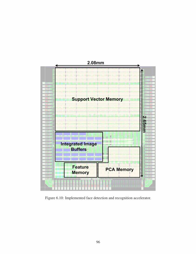
Figure 6.10: Implemented face detection and recognition accelerator.
96

6.5 Implementation
The proposed face detection and recognition accelerator is implemented in 40nm CMOS tech-
nology. Fig. 6.10 shows the layout of the implemented accelerator. The area of the core is 5.51mm2
and the system operates with 81MHz clock frequency at 0.5V, which translates to 5 frames per sec-
ond throughput. The power consumption in this operating condition is only 21.7mW.
6.6 Conclusions
This chapter proposed a low power face detection and recognition accelerator targeted for
mobile applications. The proposed algorithm and architecture optimization techniques enabled
a feasible single-chip system that performs both detection and recognition and provides enough
performance for real time operation. Since the design requires only 16MHz/fps clock frequency, it
can take advantage of deep voltage scaling for even better energy efficiency in case of low through-
put requirement. The proposed 5T memory design utilizes the property of the system that it only
requires rare or one-time write operation. While maintaining smaller size than 6T, the proposed
memory shows better read operation margin due to isolated read path. The resulting accelerator
design consumes only 21.7mW while processing 5fps HD video input.
97

CHAPTER 7
Conclusions
In modern large scale SoCs, various digital signal processing algorithms are incorporated in
order to provide better user experience across different application areas. Technology scaling
has enabled hardware implementation of more complicated algorithms by having more transistors
in the same area, but it caused noticeable increase in power consumption and heat dissipation.
Furthermore, recent advances in signal processing (e.g., machine learning algorithms) necessitate
significantly more hardware resources, making it infeasible to rely solely on CMOS scaling ef-
fect. While algorithm and circuit designers can attempt to individually optimize in their own areas
to reduce hardware cost, considering multiple levels of design simultaneously may offer a better
opportunity. This dissertation studies various optimization techniques in different design levels
ranging from circuit techniques to algorithmic modifications using DSP hardwares as a test vehi-
cle. Chapter 2 proposes an extremely energy-efficient FFT processor based on proper architecture
selection that takes into account leakage energy in low operating voltage. Also, latch-based mem-
ory contributes to save energy consumption by lowering minimum operating voltage. In Chapter
3, voltage-overscaling is studied and a simple but accurate timing error model is proposed. De-
signing voltage-overscaled system often requires many iterations and numerous simulations. How-
ever, by combining algorithm or system level error management with the proposed simple model,
a low-power K-best decoder is implemented with a simple timing error detection circuitry. In
Chapter 4, co-optimization technique advances further, where circuit, architecture and algorithm
are considered altogether. A low-power VGA full-frame feature extraction processor is realized
using shift-latch FIFO and modified SURF algorithm. Chapter 5 describes system level optimiza-
98

tion that minimizes energy consumption to achieve the given operation in the system including
both analog and digital processing blocks. This chapter proposes an implantable ECG-monitoring
mixed-signal SoC that consumes only 64nW in the continuous monitoring mode. Finally, Chap-
ter 6 focuses more on circuit technique and proposes a single chip face detection that employs an
application-specific SRAM design and architecture optimizations.
Although several optimization techniques across different design levels are considered in this
dissertation, there still exist many other areas in need of further studies. A complete and unified
design framework for hardware and algorithm co-optimization that can be applied to general DSP
applications will make huge progress toward realizing more advanced signal processing algorithms
in hardware. In addition, digital processing blocks are mainly studied in this dissertation, but most
of modern SoCs also have a lot of analog blocks such as radios, sensors and sensor interfaces.
Frequently power consumption in those domains exceed the one in the digital domain; therefore,
integrating them into the optimization flows covered in this dissertation is another important step.
99

BIBLIOGRAPHY
100

[1] G. Chen, M. Fojtik, D. Kim, D. Fick, J. Park, M. Seok, M.-T. Chen, Z. Foo, D. Sylvester, andD. Blaauw, “Millimeter-scale nearly perpetual sensor system with stacked battery and solarcells,” in IEEE Int. Solid-State Circuits Conf. Dig. Tech. Papers, Feb. 2010, pp. 288-289.
[2] Y. Lee, G. Kim, S. Bang, Y. Kim, I. Lee, P. Dutta, D. Sylvester, and D. Blaauw, “A modu-lar 1mm3 die-stacked sensing platform with optical communication and multi-modal energyharvesting,” in IEEE Int. Solid-State Circuits Conf. Dig. Tech. Papers, Feb. 2012, pp. 402-404.
[3] http://www.arm.com/products/processors/cortex-m/cortex-m4-processor.php.
[4] Y. Park, C. Yu, K. Lee, H. Kim, Y. Park, C. Kim, Y. Choi, J. Oh, C. Oh, G. Moon, S. Kim, H.Jang, J.-A. Lee, C. Kim, and S. Park, “72.5GFLOPS 240Mpixel/s 1080p 60fps multi-formatvideo codec application processor enabled with GPGPU for fused multimedia application,” inIEEE Int. Solid-State Circuits Conf. Dig. Tech. Papers, Feb. 2013, pp. 160-161.
[5] P. N. Whatmough, S. Das, and D. M. Bull, “A low-power 1GHz razor FIR accelerator withtime-borrow tracking pipeline and approximate error correction in 65nm CMOS,” in IEEE Int.Solid-State Circuits Conf. Dig. Tech. Papers, Feb. 2013, pp. 428-429.
[6] C.-T. Huang, M. Tikekar, C. Juvekar, V. Sze, and A. Chandrakasan, “A 249Mpixel/s HEVCvideo-decoder chip for Quad Full HD applications,” in IEEE Int. Solid-State Circuits Conf.Dig. Tech. Papers, Feb. 2013, pp. 162-163.
[7] R. Rithe, P. Raina, N. Ickes, S. V. Tenneti, and A. P. Chandrakasan, “Reconfigurable Processorfor Energy-Scalable Computational Photography,” in IEEE Int. Solid-State Circuits Conf. Dig.Tech. Papers, Feb. 2013, pp. 164-165.
[8] Y. S. Park, Y. Tao, and Z. Zhang, “A 1.15Gb/s fully parallel nonbinary LDPC decoder withfine-grained dynamic clock gating,” in IEEE Int. Solid-State Circuits Conf. Dig. Tech. Papers,Feb. 2013, pp. 422-423.
[9] B. Zhai, D. Blaauw, D. Sylvester, and K. Flautner, “Theoretical and Practical Limits of Dy-namic Voltage Scaling,” in Proc. Design Automation Conf., May 2005, pp. 868-873.
[10] B. Zhai, S. Pant, L. Nazhandali, S. Hanson, J. Olson, A. Reeves, M. Minuth, R. Helfand,T. Austin, D. Sylvester, and D. Blaauw, “Energy-Efficient Subthreshold Processor Design,”IEEE Trans. on VLSI Systems, vol. 17, no. 8, pp. 1127-1137, Aug. 2009.
[11] B. Zhai, S. Hanson, D. Blaauw, and D. Sylvester, “A Variation-Tolerant Sub-200 mV 6-TSubthreshold SRAM,” IEEE J. Solid-State Circuits, vol. 43, no. 10, pp. 2338-2348, Oct. 2008.
[12] H. Fuketa, M. Hashimoto, Y. Mitsuyama, and T. Onoye, “Adaptive Performance Compensa-tion with In-Situ Timing Error Prediction for Subthreshold Circuits,” in Proc. IEEE CustomIntegrated Circuits Conf., Sep. 2009, pp. 215-218.
[13] D. Ernst, N. S. Kim, S. Das, S. Pant, R. Rao, T. Pham, C. Ziesler, D. Blaauw, T. Austin,K. Flautner, and T. Mudge, “Razor: A Low-Power Pipeline Based on Circuit-Level TimingSpeculation,” in Proc. Int. Symp. Microarchitecture, Dec. 2003, pp. 7-18.
101

[14] M. Fojtik, D. Fick, Y. Kim, N. Pinckney, D. Harris, D. Blaauw, and D. Sylvester, “BubbleRazor: An architecture-independent approach to timing-error detection and correction,” inIEEE Int. Solid-State Circuits Conf. Dig. Tech. Papers, Feb. 2012, pp. 488-490.
[15] R. A. Abdallah and N. R. Shanbhag, “Error-Resilient Low-Power Viterbi Decoder Architec-tures,” IEEE Trans. on Signal Processing, pp. 4906-4917, 2009.
[16] J. Zhou, D. Zhou, G. He, and S. Goto, “A 1.59Gpixel/s motion estimation processor with?211-to-211 search range for UHDTV video encoder,” in Proc. IEEE Symp. VLSI Circuits,Jun. 2013, pp. 286-287.‘
[17] S. R. Sridhara, M. DiRenzo, S. Lingam, S.-J. Lee, R. Blazquez, J. Maxey, S. Ghanem, Y.-H. Lee, R. Abdallah, P. Singh, and M. Goel, “Microwatt Embedded Processor Platform forMedical System-on-Chip Applications,” IEEE J. Solid-State Circuits, vol. 46, no. 4, pp. 721-730, Apr. 2011.
[18] B. Zhai, S. Hanson, D. Blaauw, and D. Sylvester, “Analysis and Mitigation of Variability inSubthreshold Design,” in Proc. Int. Symp. Low Power Electronics and Design, Aug. 2005, pp.20-25.
[19] A. Wang and A. Chandrakasan, “A 180-mV subthreshold FFT processor using a minimumenergy design methodology,” IEEE J. Solid-State Circuits, vol. 40, no. 1, pp. 310-319, Jan.2005.
[20] B. M. Baas, “A low-power, high-performance, 1024-point FFT processor,” IEEE J. Solid-State Circuits, vol. 34, no. 3, pp. 380-387, Mar. 1999.
[21] M. Seok, D. Jeon, C. Chakrabarti, D. Blaauw, and D. Sylvester, “A 0.27V 30MHz17.7nJ/transform 1024-pt Complex FFT Core with Super-Pipelining,” in IEEE Int. Solid-StateCircuits Conf. Dig. Tech. Papers, Feb. 2011, pp. 342-343.
[22] V. Srinivasan, D. Brooks, M. Gschwind, P. Bose, V. Zyuban, P. N. Strenski, and P. G. Emma,“Optimizing Pipelines for Power and Performance,” in Proc. Int. Symp. Microarchitecture,Nov. 2002, pp. 333-344.
[23] M. S. Hrishikesh, N. P. Jouppi, K. I. Farkas, D. Burger, S. W. Keckler, and P. Shivakumar,“The optimal logic depth per pipeline stage is 6 to 8 FO4 inverter delays,” in Proc. Int. Symp.Computer Architecture, May 2002, pp. 14-24.
[24] A. Chandrakasan and R. Brodersen, Low-Power CMOS Design, New York, Wiley-IEEEPress, 1998.
[25] M. Seok, S. Hanson, Y.-S. Lin, Z. Foo, D. Kim, Y. Lee, N. Liu, D. Sylvester, and D. Blaauw,“The Phoenix Processor: A 30pW Platform for Sensor Applications,” in Proc. IEEE Symp.VLSI Circuits, Jun. 2008, pp. 188-189.
[26] B. H. Calhoun, A. Wang and A. Chandrakasan, “Modeling and Sizing for Minimum EnergyOperation in Subthreshold Circuits,” J. Solid-State Circuits, vol. 40, no. 9, pp. 1778-1786,Sep. 2005.
102

[27] S. Hanson, B. Zhai, M. Seok, B. Cline, K. Zhou, M. Singhal, M. Minuth, J. Olson, L. Nazhan-dali, T. Austin, D. Sylvester and D. Blaauw, “Performance and Variability Optimization Strate-gies in a Sub-200mV, 3.5pJ/inst, 11nW Subthreshold Processor,” in Proc. IEEE Symp. VLSICircuits, Jun. 2007, pp. 152-153.
[28] D. Harris, Skew-Tolerant Circuit Design, Burlington, Morgan Kaufmann, 2000.
[29] M. Wieckowski, Y. M. Park, C. Tokunaga, D. W. Kim, Z. Foo, D. Sylvester, and D. Blaauw,“Timing yield enhancement through soft edge flip-flop based design,” in Proc. IEEE CustomIntegrated Circuits Conf., Sep. 2008, pp. 543-546.
[30] H. Ando, Y. Yoshida, A. Inoue, I. Sugiyama, T. Asakawa, K. Morita, T. Muta, T. Motokuru-mada, S. Okada, H. Yamashita, Y. Satsukawa, A. Konmoto, R. Yamashita, and H. Sugiyama,“A 1.3-GHz fifth-generation SPARC64 microprocessor,” IEEE J. Solid-State Circuits, vol. 38,no. 11, pp. 1896-1905, Nov. 2003.
[31] S. He and M. Torkelson, “A new approach to pipeline FFT processor,” in Proc. Int. ParallelProcessing Symp., Apr. 1996, pp. 766-770.
[32] W. Tang and L. Wang, “Cooperative OFDM for energy efficient wireless sensor networks,”in Proc. IEEE Workshop on Signal Processing Systems, Oct. 2008, pp. 77-82.
[33] D. Zhao, H. Ma and L. Liu, “Event classification for living environment surveillance usingaudio sensor networks,” in Proc. IEEE Int. Conf. Multimedia and Expo, Jul. 2010, pp. 528-533.
[34] E. E. Swartzlander, W. K. W. Young, and S. J. Joseph, “A radix 4 delay commutator for fastFourier transform processor implementation,” IEEE J. Solid-State Circuits, vol. 19, no. 5, pp.702-709, Oct. 1984.
[35] T. Gemmeke, M. Gansen, H. J. Stockmanns, and T. G. Noll, “Design Optimization of Low-Power High-Performance DSP Building Blocks,” IEEE J. Solid-State Circuits, vol. 39, no. 7,pp. 1131-1139, Jul. 2004.
[36] S. Yoshizawa, K. Nishi, and Y. Miyanaga, “Reconfigurable Two-Dimensional Pipeline FFTProcessor in OFDM Cognitive Radio Systems,” in Proc. IEEE Int. Symp. Circuits and Systems,May. 2008, pp. 1248-1251.
[37] C.-C. Wang, J.-M. Huang, and H.-C. Cheng, “A 2K/8K Mode Small-Area FFT Processor forOFDM Demodulation of DVB-T Receivers,” IEEE Trans. Consumer Electronics, vol. 51, no.1, pp. 28-32, Feb. 2005.
[38] B. H. Calhoun and A. P. Chandrakasan, “A 256-kb 65-nm Sub-threshold SRAM Design forUltra-Low-Voltage Operation,” IEEE J. Solid-State Circuits, vol. 42, no. 3, pp.680-688, Mar.2007.
[39] C.-H. Lo, S.-Y. Huang, “P-P-N Based 10T SRAM Cell for Low-Leakage and ResilientSubthreshold Operation,” IEEE J. Solid-State Circuits, vol. 46, no. 3, pp. 520-529, Mar. 2011.
103

[40] M.-F. Chang, S.-W. Chang, P.-W. Chou, and W.-C. Wu, “A 130 mV SRAM With ExpandedWrite and Read Margins for Subthreshold Applications,” IEEE J. Solid-State Circuits, vol. 46,no. 2, pp. 520-529, Feb. 2011.
[41] M. Seok, D. Blaauw, and D. Sylvester, “Clock network design for ultra-low power applica-tions,” in Proc. Int. Symp. Low Power Electronics and Design, Aug. 2010, pp. 271-276.
[42] Y. Chen, Y.-W. Lin, Y.-C. Tsao, and C.-Y. Lee, “A 2.4-Gsample/s DVFS FFT Processor forMIMO OFDM Communication Systems,” IEEE J. Solid-State Circuits, vol. 43, no. 5, pp.1260-1273, May. 2008.
[43] C.-H. Yang, T.-H. Yu, and D. Markovic, “A 5.8mW 3GPP-LTE Compliant 88 MIMO SphereDecoder Chip with Soft-Outputs,” in Proc. IEEE Symp. VLSI Circuits, Jun. 2010, pp. 209-210.
[44] A. Wang, A. P. Chandrakasan, and S. V. Kosonocky, “Optimal supply and threshold scalingfor subthreshold CMOS circuits,” in Proc. IEEE Computer Society Annual Symp. on VLSI, pp.5-9, 2002.
[45] D. Blaauw, S. Kalaiselvan, K. Lai, W.-H. Ma, S. Pant, C. Tokunaga, S. Das, D. Bull, “RazorII: In Situ Error Detection and Correction for PVT and SER Tolerance,” in Proc. IEEE Int.Solid-State Circuits Conf., pp. 400-401, 2008.
[46] G. V. Varatkar and N. R. Shanbhag, “Error-Resilient Motion Estimation Architecture,” IEEETrans. on VLSI Systems, pp. 1399-1412, 2008.
[47] Y. Liu and T. Zhang, “On the Selection of Arithmetic Unit Structure in Voltage OverscaledSoft Digital Signal Processing,” in Proc. ACM/IEEE Int. Symp. on Low Power Electronics andDesign, pp. 250-255, 2007.
[48] A. B. Kahng, S. Kang, R. Kumar, J. Sartori, “Slack Redistribution for Graceful DegradationUnder Voltage Overscaling,” in Proc. 15th Asia and South Pacific Design Automation Conf.,pp. 825-831, 2010.
[49] Y. Liu, T. Zhang, K. K. Parhi, “Computation Error Analysis in Digital Signal ProcessingSystems With Overscaled Supply Voltage,” IEEE Trans. on VLSI Systems, pp. 517-526, 2009.
[50] Y. Liu, T. Zhang, J. Hu, “Design of Voltage Overscaled Low-Power Trellis Decoders inPresence of Process Variations,” IEEE Trans. on VLSI Systems, pp. 439-443, 2008.
[51] Z. Guo and P. Nilsson, “Algorithm and implementation of the K-best sphere decoding forMIMO detection,” IEEE Journal on Selected Areas in Communications, pp. 491-503, 2006.
[52] M. Shabany and P. G. Gulak, “A 0.13m CMOS 655Mb/s 4x4 64-QAM K-Best MIMO De-tector,” in Proc. IEEE Int. Solid-State Circuits Conf., pp. 256-257, 2009.
[53] J. Zheng, D. Kuai, Z. Liu, Y. Teng, and T. Zhang, “Salient Feature Volume and Its Appli-cation in Brain MRI Image Registration,” in Proc. Int. Conf. on Biomedical Engineering andInformatics, Oct. 2011, pp. 477-481.
104

[54] M. P. Heinrich, M. Jenkinson, M. Brady, and J. A. Schnabel, “MRF-Based DeformableRegistration and Ventilation Estimation of Lung CT,” IEEE Trans. on Medical Imaging, vol.32, no. 7, pp. 1239-1248, Jul. 2013.
[55] P. Kumar, A. Mittal, and P. Kumar, “A multimodal audio visible and infrared surveillancesystem (MAVISS),” in Proc. Int. Conf. on Intelligent Sensing and Information Processing,Dec. 2005, pp. 151-156.
[56] S. Segvic, A. Remazeilles, A. Diosi, and F. Chaumette, “Large scale vision-based navigationwithout an accurate global reconstruction,” in Proc. IEEE Conf. on Computer Vision andPattern Recognition, Jun. 2007, pp. 1-8.
[57] Y. Zhang, F. Zhang, Y. Shakhsheer, J. D. Silver, A. Klinefelter, M. Nagaraju, J. Boley, J.Pandey, A. Shrivastava, E. J. Carlson, A. Wood, B. H. Calhoun, and B. P. Otis, “A Batteryless19µW MICS/ISM-Band Energy Harvesting Body Sensor Node SoC for ExG Applications,”IEEE J. Solid-State Circuits, vol. 48, no. 1, pp. 199-213, Jan. 2013.
[58] D. G. Lowe, “Object recognition from local scale-invariant features,” in Proc. IEEE Int.Conf. on Computer Vision, Sep. 1999, pp. 1150-1157.
[59] H. Bay, A. Ess, T. Tuytelaars, and L. V. Gool, “SURF: Speeded Up Robust Features,” Com-puter Vision and Image Understanding, vol. 110, no. 3, pp. 346-359, 2008.
[60] S. Shen, N. Michael, and V. Kumar, “Autonomous Multi-Floor Indoor Navigation with aComputationally Constrained MAV,” in Proc. IEEE Conf. on Robotics and Automation, May2011, pp. 20-25.
[61] S. Lee, J. Oh, M. Kim, J. Park, J. Kwon, and H.-J. Yoo, “A 345mW Heterogeneous Many-Core Processor with an Intelligent Inference Engine for Robust Object Recognition,” in IEEEInt. Solid-State Circuits Conf. Dig. Tech. Papers, Feb. 2010, pp. 332-333.
[62] Y.-C. Su, K.-Y. Huang, T.-W. Chen, Y.-M. Tsai, S.-Y. Chen, and L.-G. Chen, “A 52mWfull HD 160-degree object viewpoint recognition SoC with visual vocabulary processor forwearable vision applications,” in Proc. IEEE Symp. on VLSI Circuits, Jun. 2011, pp. 258-259.
[63] J. Oh, G. Kim, J. Park, I. Hong, S. Lee, and H.-J. Yoo, “A 320mW 342GOPS real-timemoving object recognition processor for HD 720p video streams,” in IEEE Int. Solid-StateCircuits Conf. Dig. Tech. Papers, Feb. 2012, pp. 220-222.
[64] Y.-M. Tsai, T.-J. Yang, C.-C. Tsai, K.-Y. Huang, and L.-G. Chen, “A 69mW 140-meter/60fpsand 60-meter/300fps intelligent vision SoC for versatile automotive applications,” in Proc.IEEE Symp. on VLSI Circuits, Jun. 2012, pp. 152-153.
[65] S. A. J. Winder and M. Brown, “Learning Local Image Descriptors,” in Proc. IEEE Conf. onComputer Vision and Pattern Recognition, Jun. 2007, pp. 1-8.
[66] F.-C. Huang, S.-Y. Huang, J.-W. Ker, and Y.-C. Chen, “High-Performance SIFT HardwareAccelerator for Real-Time Image Feature Extraction,” IEEE Trans. on Circuits and Systemsfor Video Technology, vol. 22, no. 3, pp. 340-351, Mar. 2012.
105

[67] I. J. Chang, J.-J. Kim, S. P. Park, and K. Roy, “A 32 kb 10T Sub-Threshold SRAM ArrayWith Bit-Interleaving and Differential Read Scheme in 90 nm CMOS,” IEEE J. Solid-StateCircuits, vol. 44, no. 2, pp. 650-658, Feb. 2009.
[68] C. Zellerhoff, E. Himmrich, D. Nebeling, O. Przibille, B. Nowak, and A. Liebrich, “Howcan we identify the best implantation site for an ECG event recorder?,” Pacing & ClinicalElectrophys, pp. 1545-1549, Oct. 2000.
[69] R. F. Yazicioglu, S. Kim, T. Torfs, H. Kim, and C. Van Hoof, “A 30uW Analog SignalProcessor ASIC for Portable Biopotential Signal Monitoring,” IEEE J. Solid-State Circuits,vol. 46, no. 1, pp. 209-223, Jan. 2011.
[70] H. Zhang, Y. Qin, S. Yang, and Z. Hong, “Design of an ultra-low power SAR ADC forbiomedical applications,” in Proc. IEEE Conf. on Solid-State and Integrated Circuit Technol-ogy, Nov. 2010, pp. 460-462.
[71] F. Zhang, Y. Zhang, J. Silver, Y. Shakhsheer, M. Nagaraju, A. Klinefelter, J. Pandey, J. Boley,E. Carlson, A. Shrivastava, B. Otis, and B. Calhoun, “A batteryless 19uW MICS/ISM-bandenergy harvesting body area sensor node SoC,” in IEEE Int. Solid-State Circuits Conf. Dig.Tech. Papers, Feb. 2012, pp. 298-300.
[72] S.-Y. Hsu, Y. Ho, Y. Tseng, T.-Y. Lin, P.-Y. Chang, J.-W. lee, J.-H. Hsiao, S.-M. Chuang, T.-Z. Yang, P.-C. Liu, T.-F. Yang, R.-J. Chen, C. Su, C.-Y. Lee, “A sub-100uW multi-functionalcardiac signal processor for mobile healthcare applications,” in Proc. IEEE Symp. on VLSICircuits, Jun. 2012, pp. 156-157.
[73] S. Kim, L. Yan, S. Mitra, M. Osawa, Y. Harada, K. Tamiya, C. Van Hoof, R. F. Yazicioglu,“A 20uW intra-cardiac signal-processing IC with 82dB bio-impedance measurement dynamicrange and analog feature extraction for ventricular fibrillation detection,” in IEEE Int. Solid-State Circuits Conf. Dig. Tech. Papers, Feb. 2013, pp. 302-303.
[74] P. Viola and M. Jones, “Rapid Object Detection using a Boosted Cascade of Simple Features,”in Proc. IEEE Conf. on Computer Vision and Pattern Recognition, Jun. 2001, pp. I.511-I.518.
[75] Y. Hanai, Y. Hori, J. Nishimura, and T. Kuroda, “A versatile recognition processor employingHaar-like feature and cascaded classifier,” in IEEE Int. Solid-State Circuits Conf. Dig. Tech.Papers, Feb. 2009, pp. 148-149.
[76] M. A. Turk, A. P. Pentland, “Face recognition using eigenfaces,” in Proc. IEEE Conf. onComputer Vision and Pattern Recognition, Jun. 1991, pp. 586-591.
[77] Z. Wang, S. Wang, Y. Zhu, and Q. Ji, “Bias analyses of spontaneous facial expressiondatabase,” in IEEE Int. Conf. on Pattern Recognition, Nov. 2012, pp. 2926-2929.
[78] K. H. Lee and N. Verma, “A Low-Power Processor With Configurable Embedded Machine-Learning Accelerators for High-Order and Adaptive Analysis of Medical-Sensor Signals,”IEEE J. Solid-State Circuits, vol. 48, no. 7, pp. 1625-1637, Jul. 2013.
106

[79] J.-C. Wang, L.-X. Lian, and J.-H. Zhao, “VLSI Design for SVM-Based Speaker VerificationSystem,” IEEE Trans. on VLSI Systems, to appear.
[80] G. kim, Y. Kim, K. Lee, S. Park, I. Hong, K. Bong, D. Shing, S. Choi, J. Oh, H.-J. Yoo, “A1.22TOPS and 1.52mW/MHz Augmented Reality Multi-Core Processor with Neural NetworkNoC for HMD Applications,” in IEEE Int. Solid-State Circuits Conf. Dig. Tech. Papers, Feb.2014, pp. 182-183.
[81] G. B. Huang, V. Jain, and E. Learned-Miller, “Unsupervised joint alignment of compleximages,” in Proc. IEEE Int. Conf. on Computer Vision, Oct. 2007, pp. 1-8.
[82] M.-P. Chen, L.-F. Chen, M.-F. Chang, S.-M. Yang, Y.-J. Kuo, J.-J. Wu, M.-S. Ho, H.-Y. Su,Y.-H. Chu, W.-C. Wu, T.-Y. Yang, and H. Yamauchi, “A 260mV L-shaped 7T SRAM with bit-line (BL) Swing expansion schemes based on boosted BL, asymmetric-VTH read-port, andoffset cell VDD biasing techniques,” in Proc. IEEE Symp. on VLSI Circuits, Jun. 2012, pp.112-113.
107