Embed Size (px)
Citation preview
Efrain Altamirano-Sanchez & Jean Francois de Marneffe
End-of-CMOS and beyond CMOS applications for Atomic Layer Etching
ETCH/UPM/IMEC

2
DTCO
STCO
Logic Roadmap view
log 2
(#tr
ansi
sto
rs/$
)
20152013201120092007
Happy scaling era# transistors per area
doubles every two yearfor same cost
14nm
20nm
28nm
40nm
65nm
90nm
Less happy scaling eraStill doubles but device
scaling provides diminishing returns
2017 2019 2021 2023 20252005
Heterogenous scaling2D Material for power gatingBack Side PDN MRAM….
20nm: First sign of troubleDouble patterning (cost !)Planar device runs out of steam
14nm: FinFETFinFET device saves the day
10nm7nm
5nm
7-5nm: At last ...EUV reduces cost
4-3nm:Nanowire/sheet FET to continue gate length scaling
3nm
2nm1.5nm
10-7nm: More troubleMulti-patterning cost escalates
Scaling boosters
Focus of process technology innovation is
Scale device and wire Scale basic logic cells Scale (sub-)system functions
Track height reduction
New ComputeMachine learningQuantum computingCryogenic electronics
2nm:High NA EUV?
2

Basic principle of ALE and Quasi-ALE
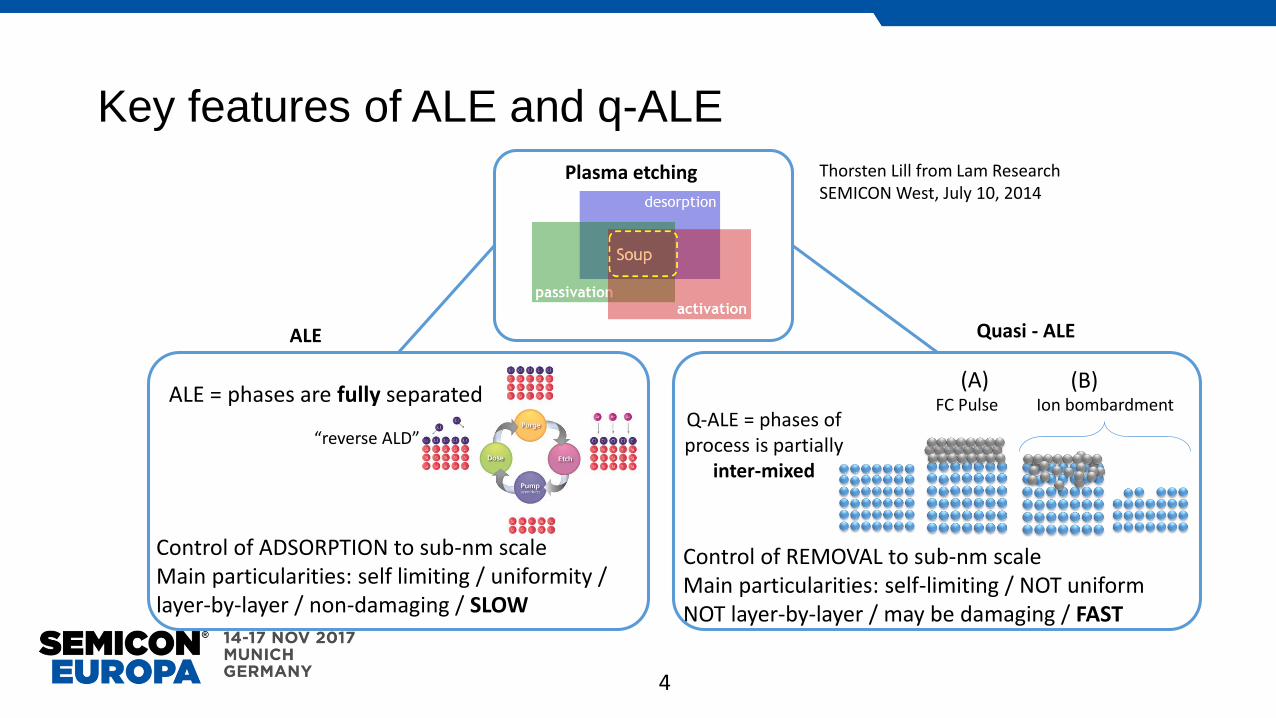
Key features of ALE and q-ALE
4
Control of REMOVAL to sub-nm scaleMain particularities: self-limiting / NOT uniformNOT layer-by-layer / may be damaging / FAST
Control of ADSORPTION to sub-nm scaleMain particularities: self limiting / uniformity / layer-by-layer / non-damaging / SLOW
Q-ALE = phases of process is partially
inter-mixed
ALE = phases are fully separated
Plasma etching
ALE
“reverse ALD”
Quasi - ALE
Thorsten Lill from Lam ResearchSEMICON West, July 10, 2014
FC Pulse Ion bombardment(A) (B)
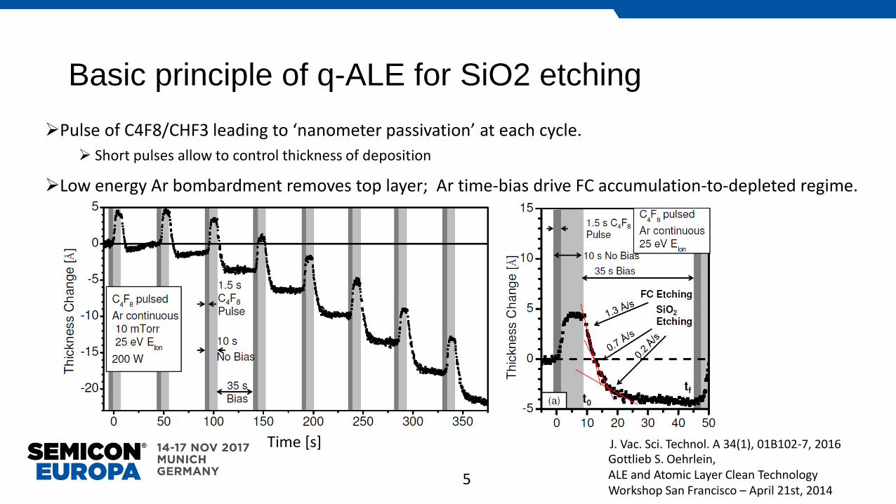
Basic principle of q-ALE for SiO2 etching
Pulse of C4F8/CHF3 leading to ‘nanometer passivation’ at each cycle.
Short pulses allow to control thickness of deposition
Low energy Ar bombardment removes top layer; Ar time-bias drive FC accumulation-to-depleted regime.
5
Gottlieb S. Oehrlein,ALE and Atomic Layer Clean TechnologyWorkshop San Francisco – April 21st, 2014
J. Vac. Sci. Technol. A 34(1), 01B102-7, 2016Time [s]
Quasi-ALE CMOS scaling

Quasi-ALE in N5 technology node
7
DECDiamond EPI contact
WACWrapped Around contact
Fin patt. Gate patt. N& P WFM Metal gate SiN gate cap M0A contact etch
Contact metallization
N&P EPI

Series resistance: contact scheme, M0A material, contact resistivity
DECDiamond EPI contact
WACWrapped Around contact
1 FIN, HFIN 50 nm
Tungsten Cobalt Ruthenium
WAC
DEC
Results of TCAD simulation based on cell layouts
Local interconnect M0A plugs options: Single local interconnect Material – Liner thickness + barrier thickness
W-M0A: Tungsten, 3 nm + 2 nmCo-M0A: Cobalt, 3 nm + 2 nmRu-M0A: Ruthenium, 1.2 nm + 0.1 nm
Contact resistivity:Rho 0.5 and 1 [x 1e-9 Ohm.cm2 ]
8
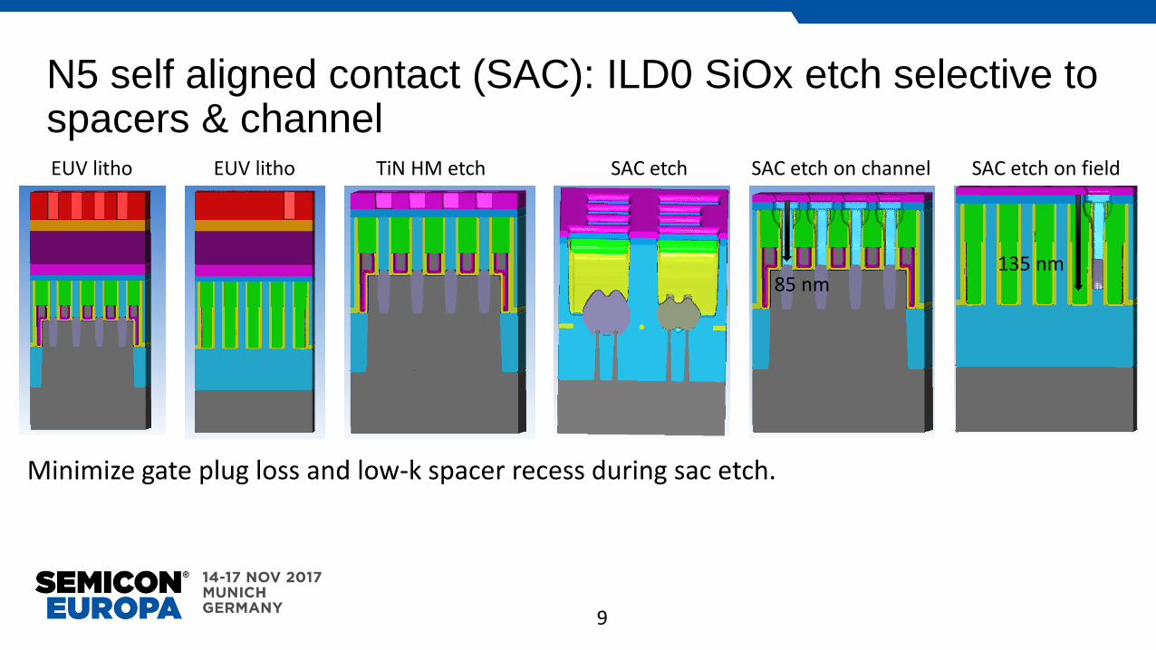
N5 self aligned contact (SAC): ILD0 SiOx etch selective to spacers & channel
9
Minimize gate plug loss and low-k spacer recess during sac etch.
135 nm85 nm
EUV litho EUV litho TiN HM etch SAC etch SAC etch on channel SAC etch on field
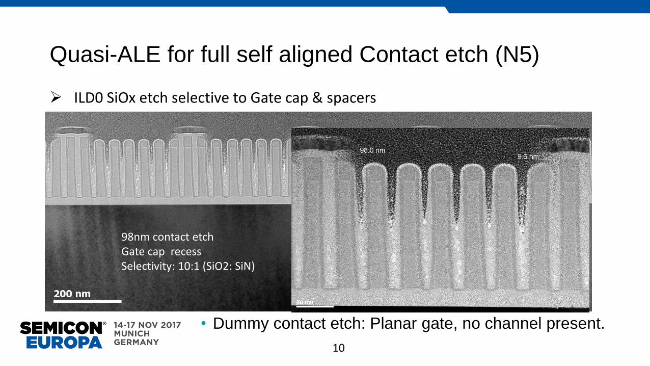
Quasi-ALE for full self aligned Contact etch (N5)
• Dummy contact etch: Planar gate, no channel present.
10
98nm contact etchGate cap recessSelectivity: 10:1 (SiO2: SiN)
ILD0 SiOx etch selective to Gate cap & spacers
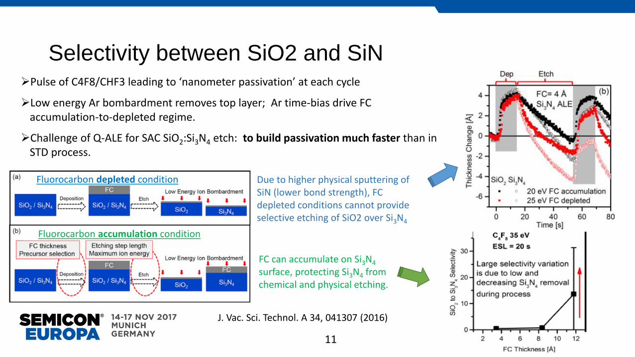
Selectivity between SiO2 and SiNPulse of C4F8/CHF3 leading to ‘nanometer passivation’ at each cycle
Low energy Ar bombardment removes top layer; Ar time-bias drive FC accumulation-to-depleted regime.
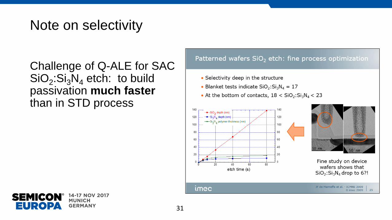
Challenge of Q-ALE for SAC SiO2:Si3N4 etch: to build passivation much faster than in STD process.
11
Fluorocarbon depleted condition
Fluorocarbon accumulation condition
Due to higher physical sputtering of SiN (lower bond strength), FC depleted conditions cannot provide selective etching of SiO2 over Si3N4
FC can accumulate on Si3N4
surface, protecting Si3N4 from chemical and physical etching.
J. Vac. Sci. Technol. A 34, 041307 (2016)
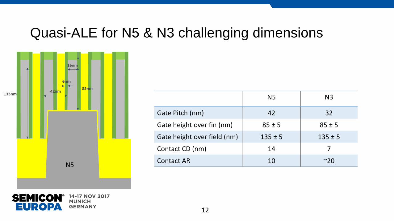
Quasi-ALE for N5 & N3 challenging dimensions
12
N5 N3
Gate Pitch (nm) 42 32
Gate height over fin (nm) 85 ± 5 85 ± 5
Gate height over field (nm) 135 ± 5 135 ± 5
Contact CD (nm) 14 7
Contact AR 10 ~20N5
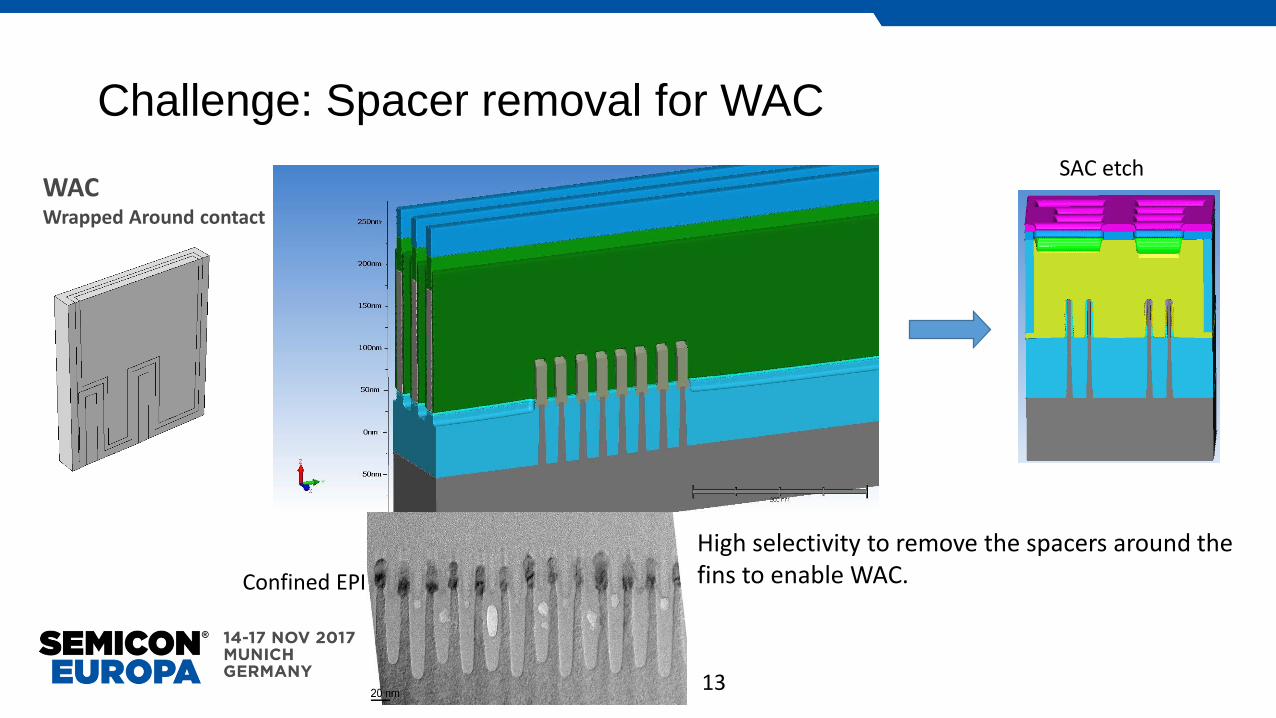
Challenge: Spacer removal for WAC
13
WACWrapped Around contact
High selectivity to remove the spacers around the fins to enable WAC.
SAC etch
Confined EPI

ALE for 2D materials

15
Benefits of 2D heterojunctions
• Vertical heterojunctions exhibit bipolar behavior with high field effect
ON/OFF ration >10^4
• Planar Heterojunctions exhibits High field effect ON/OFF ration (10^5)
and High electron mobility (m): 65 cm/Vs compared to that of isolated
multilayer.
16
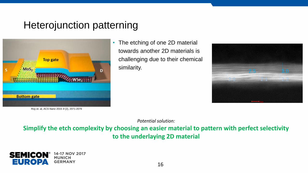
Heterojunction patterning
• The etching of one 2D material
towards another 2D materials is
challenging due to their chemical
similarity.
Potential solution:
Simplify the etch complexity by choosing an easier material to pattern with perfect selectivity to the underlaying 2D material
Roy et. al, ACS Nano 2015 9 (2), 2071-2079
2 nm2 nm2 nm2 nm2 nm
2.0 2.1 2.2
2.5 3.0
17
WS2 and MoS2 300mm deposition
MoS2 (300 mm wafer processing)
WS2 (300 mm wafer processing)
18
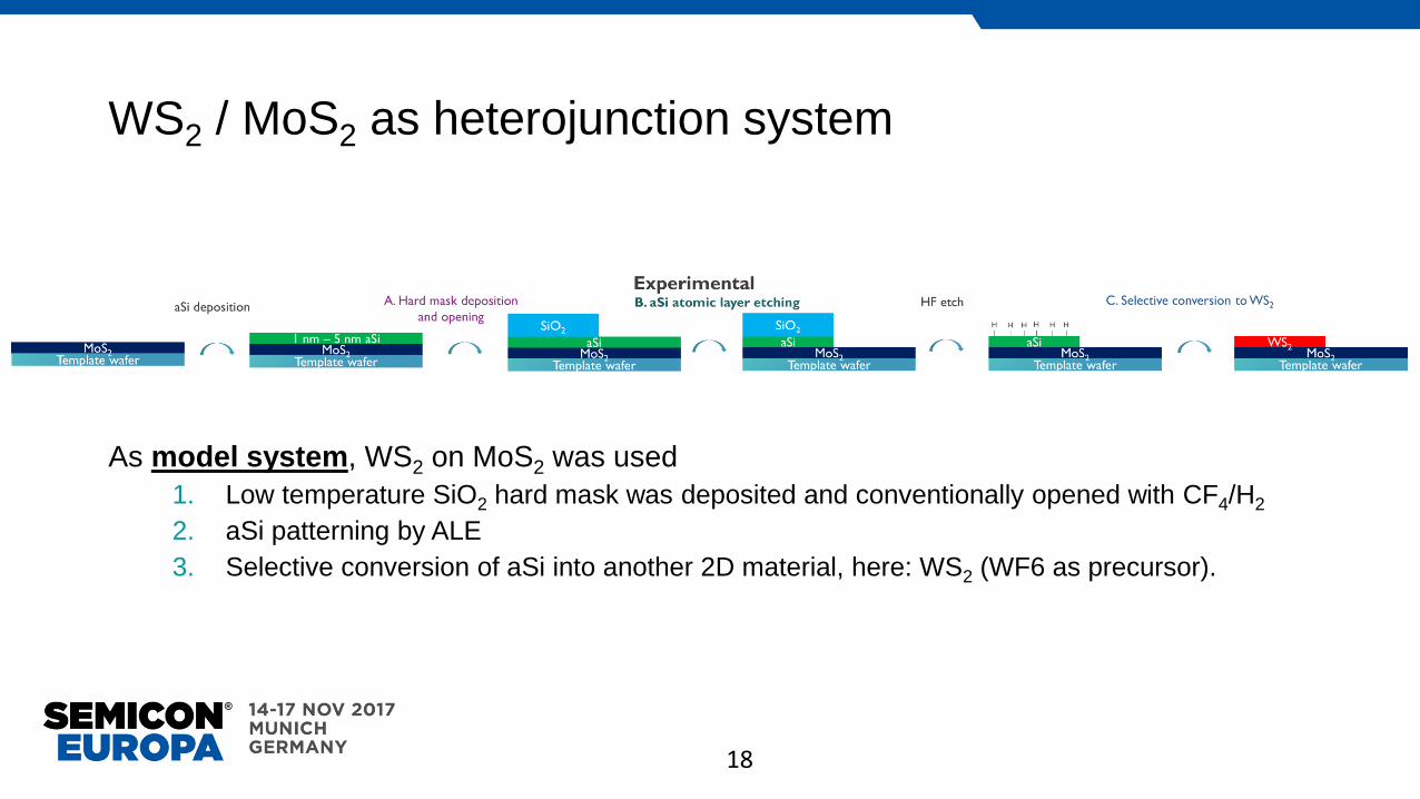
WS2 / MoS2 as heterojunction system
As model system, WS2 on MoS2 was used
1. Low temperature SiO2 hard mask was deposited and conventionally opened with CF4/H2
2. aSi patterning by ALE
3. Selective conversion of aSi into another 2D material, here: WS2 (WF6 as precursor).

19
ALE Characteristics
• Cl-based ALE has intrinsic Si etch rates
of 6 Å / cycle
Experimental verification
In agreement with literature where
chemisorption depth of 6 Å is mentioned
• Low damage towards the substrate is
expected because of the separation of
dosing and activation0
50
100
150
200
250
0 6 12 18 24
Mea
sure
d t
hic
knes
s (A
)
# cycles
Etch rate determination on amorphous silicon
Before ALE
After ALE
Linear (After ALE)
Goodyear, A.; Cooke, M.; J. Vac. Sci. Technol. A Vacuum, Surfaces, Film. 2017, 35 (1), 01A105.Patent EP 3139403, US 20170069469

20
Surface topology
After ALE surface roughness reduced
Si on MoS2
RMS = 1.077 nm
MoS2 onlyRMS = 0.962 nm
ALE towards MoS2
RMS = 0.392 nm
Template wafer
MoS2 aSiMoS2 MoS2
Template wafer
Template wafer
21
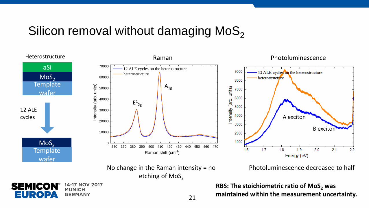
360 370 380 390 400 410 420 430 440 450 460 4700
10000
20000
30000
40000
50000
60000
70000 12 ALE cycles on the heterostructure
heterostructure
Inte
nsity (
arb
. un
its)
Raman shift (cm-1)
Raman Photoluminescence
No change in the Raman intensity = no etching of MoS2
Photoluminescence decreased to half
E12g
A1g
A exciton
B exciton
Heterostructure
12 ALEcycles
aSi
MoS2Template
wafer
MoS2Template
wafer
Silicon removal without damaging MoS2
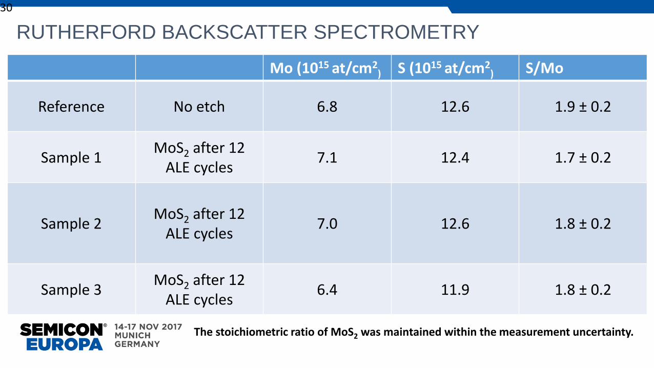
RBS: The stoichiometric ratio of MoS2 was maintained within the measurement uncertainty.
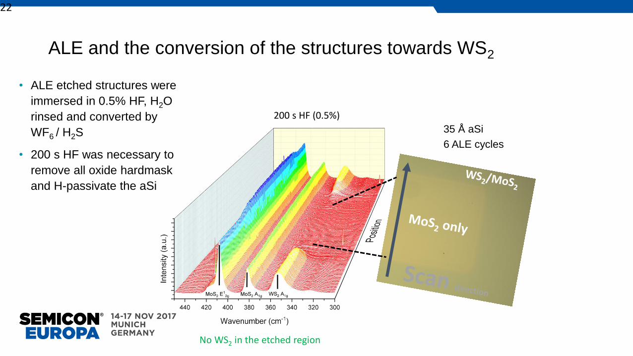
ALE and the conversion of the structures towards WS2
• ALE etched structures were
immersed in 0.5% HF, H2O
rinsed and converted by
WF6 / H2S
• 200 s HF was necessary to
remove all oxide hardmask
and H-passivate the aSi
22
No WS2 in the etched region
200 s HF (0.5%)
35 Å aSi
6 ALE cycles
ALE on Area Selective Deposition
AB
A
C
Substrate
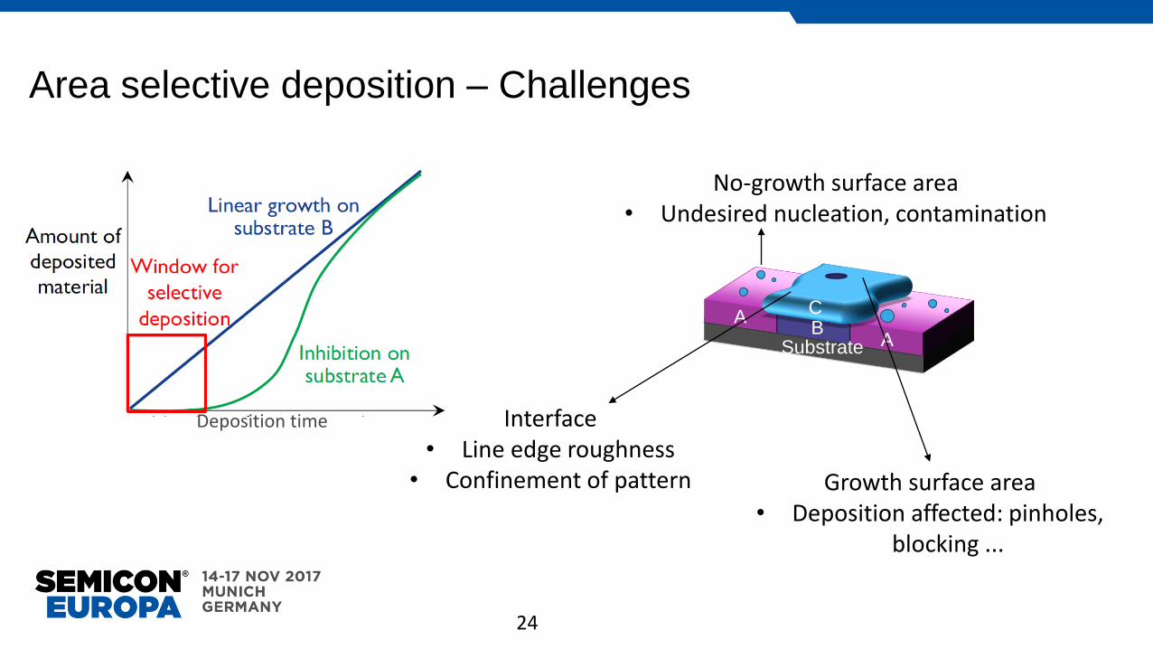
Area selective deposition – Challenges
24
Deposition time Interface• Line edge roughness
• Confinement of pattern
No-growth surface area• Undesired nucleation, contamination
Growth surface area• Deposition affected: pinholes,
blocking ...
25
Figure 3
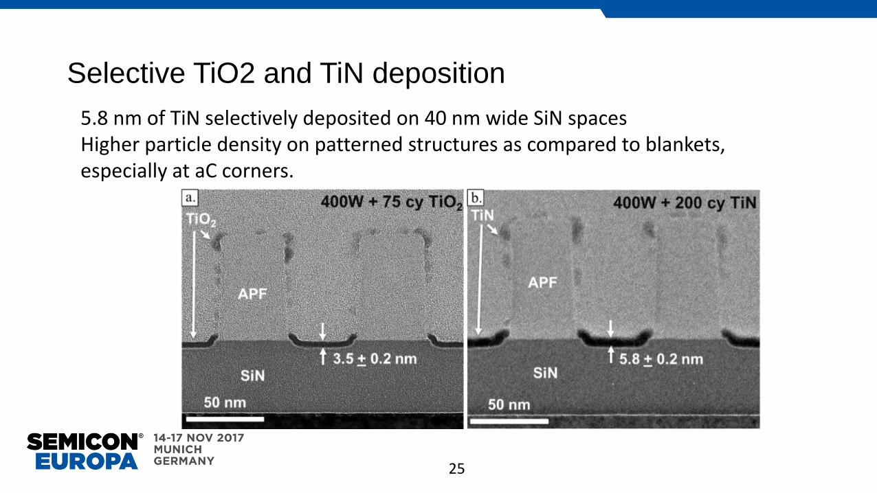
5.8 nm of TiN selectively deposited on 40 nm wide SiN spacesHigher particle density on patterned structures as compared to blankets, especially at aC corners.
Selective TiO2 and TiN deposition

26
How ‘ALE’ can help
Surface treatment
ASD
ALE of nucleates
Surface treatment
ASD
ALE of nucleates
Etc...
A tool that combines: Surface functionalization /
ALD/ALE
Thank you
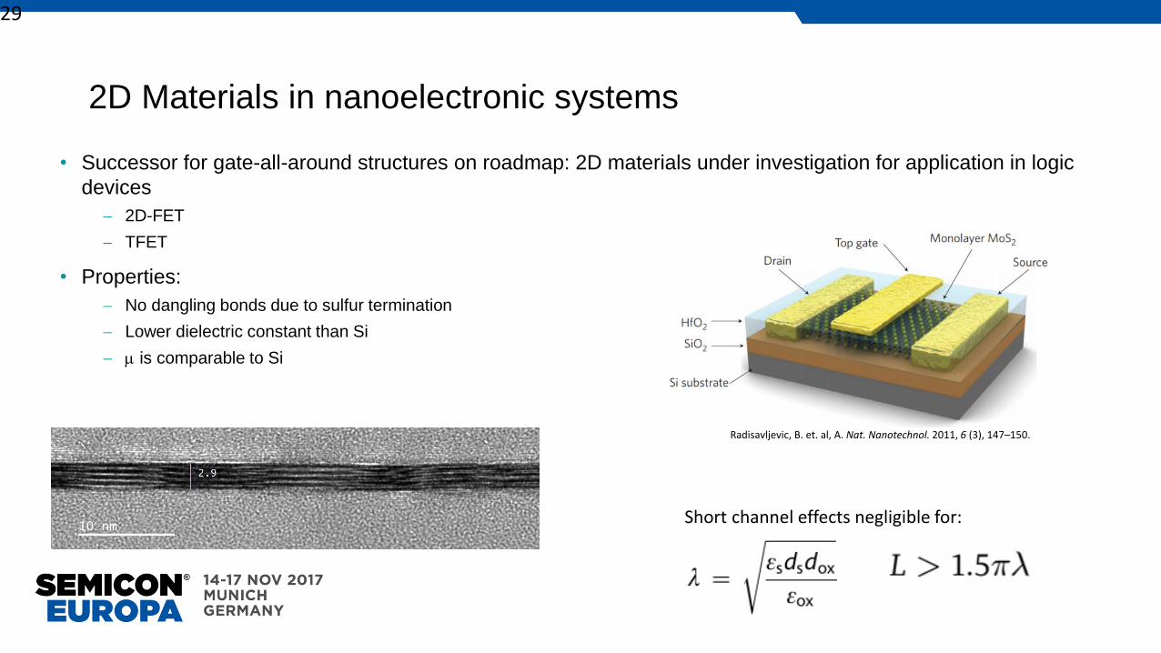
2D Materials in nanoelectronic systems
• Successor for gate-all-around structures on roadmap: 2D materials under investigation for application in logic
devices
2D-FET
TFET
• Properties:
No dangling bonds due to sulfur termination
Lower dielectric constant than Si
m is comparable to Si
29
Short channel effects negligible for:
Radisavljevic, B. et. al, A. Nat. Nanotechnol. 2011, 6 (3), 147–150.
30
Mo (1015 at/cm2) S (1015 at/cm2
) S/Mo
Reference No etch 6.8 12.6 1.9 ± 0.2
Sample 1MoS2 after 12
ALE cycles7.1 12.4 1.7 ± 0.2
Sample 2MoS2 after 12
ALE cycles7.0 12.6 1.8 ± 0.2
Sample 3MoS2 after 12
ALE cycles6.4 11.9 1.8 ± 0.2
The stoichiometric ratio of MoS2 was maintained within the measurement uncertainty.
RUTHERFORD BACKSCATTER SPECTROMETRY
Note on selectivity
Challenge of Q-ALE for SAC SiO2:Si3N4 etch: to build passivation much fasterthan in STD process
31