Embed Size (px)
Citation preview
@IJMTER-2015, All rights Reserved 31
Encoder, Decoder, Multiplexer and Demultiplexer in Quadruple
-Valued Logic System
Using Savart Plate and Spatial Light Modulator (SLM)
Animesh Bhattacharya 1, Amal K Ghosh 2 1 , 2 Department of Applied Electronics & Instrumentation Engineering, 2 Principal
Netaji Subhash Engineering College, Techno City, Garia, Kolkata-700152, India.
Abstract:The modern computation and communication technology is demanding the very fast
operational devices to meet up the present scenario with huge volume of data. In this light the trinary
and quadruple valued logic in multi-valued logic(MVL) systems may be the best solution for the future
generation of computational technology. In our previous papers we have proposed the modified trinary
number (MTN) system and also the quadruple valued logic(QVL) system using di-bit concept to meet
up the tremendous needs of speeds by exploiting the advantages of savart plates and spatial light
modulators (SLM) in the optical tree architecture (OTA). In this paper we have communicated the
implementations of encoder, decoder, multiplexer and demultiplexer in the quadruple valued logic
system.
Keywords: Di-bit; MVL; QVL; SLM; MTN
I. INTRODUCTION
Multi-valued logic is a natural extension of binary logic. More than last three decades there is a
continuous search to meet up the demand for tremendous operational speed of processing and handling a
huge volume of data. As a result many new ideas are being floated in the field of computation including
the implementation of optical processor for switching in one hand and on the other hand the logical
development from binary to multivalued logic. The major attraction for optical processors lies in the
parallel operation but it was also felt that it is possible to implement multivalued logic in optical system
using the polarization states of light beam along with the presence or absence of light [1]. The
parallelism of optical beam could not be properly utilized using cascaded single-bit operating units
therefore a signed digit number system was initiated with the pioneering works of Avizienis [2]. The
carry free operation was also suggested using a modified signed digit [3–5] or modified trinary [6]
system. The implementations of such gates also extended the activities in the area [7–12].
However, Lukasiewicz [13] who initiated the use of ternary logic based on three states has modified
it later [14–17] with an idea that four states logic is a much better proposition. This paper is an extension
of the modified trinary system [18–22] to a quadruple-valued logic system with dibit representation [23-
24]. In this paper we have implemented the quadruple-valued encoder, decoder, multiplexer and
demultiplexer.
II. QUADRUPLE VALUED LOGIC REPRESENTATIONS AND THE SYSTEM
The four-state representations of the quadruple valued logic system may be classified as the true, partly
true, partly false and the false. In this case we have considered these four states explicitly as {0, 1, 2, 3}
and their di-bit representations as {00, 01, 10, 11}. It is to be noted here that the four valued system with
states {0, 1, 2, 3} does not satisfy the basic field conditions whereas as a di-bit representation of the
form 00→0, 01→1, 10→2 and 11→3 may be used to represent a four valued logic where the basic two
valued logic are applicable [23-24]. As four is not a prime number, it cannot be considered as a field
International Journal of Modern Trends in Engineering and Research (IJMTER) Volume 02, Issue 08, [August– 2015] ISSN (Online):2349–9745 ; ISSN (Print):2393-8161
@IJMTER-2015, All rights Reserved 32
nevertheless this can be included in Galois Field GF(kr ), where k is a prime number and r is a positive
integer. The logical states, their representations and corresponding dibit representations and the state of
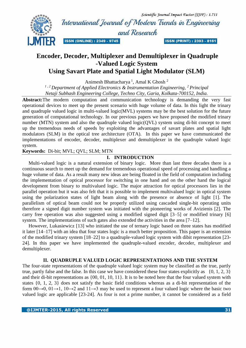
polarization is given in the Table 1. Table 1: : Quadruple-Valued Logic System
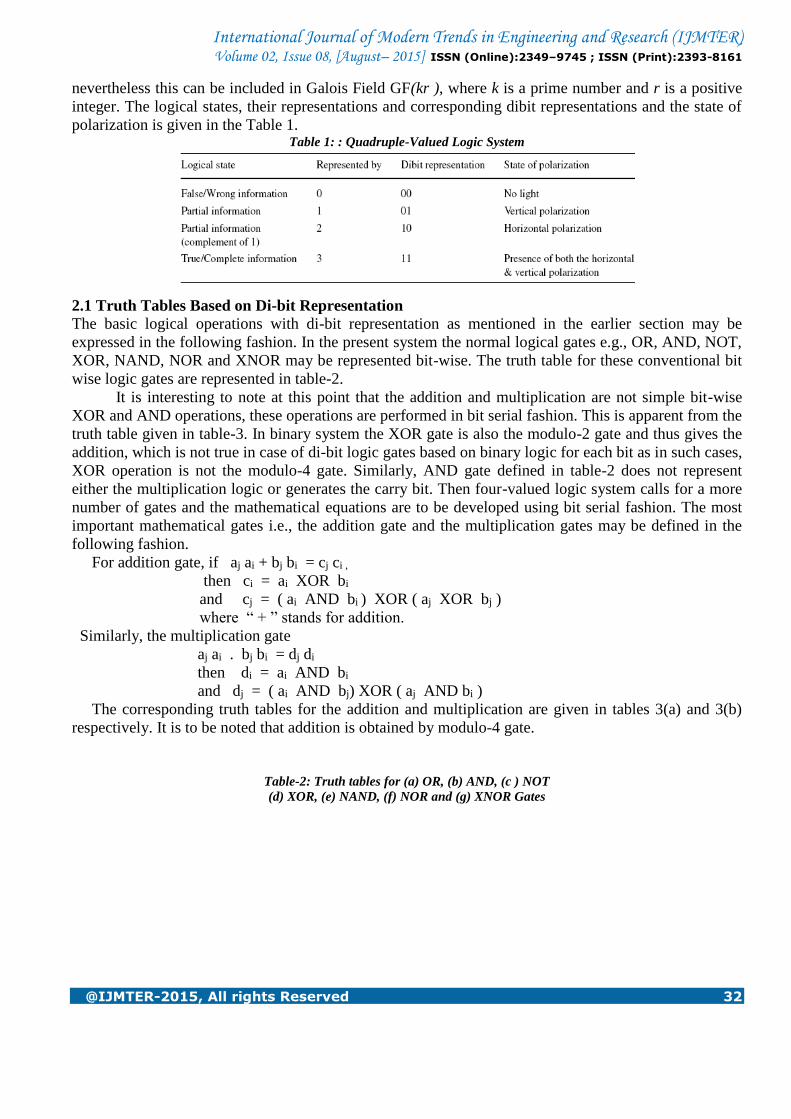
2.1 Truth Tables Based on Di-bit Representation The basic logical operations with di-bit representation as mentioned in the earlier section may be
expressed in the following fashion. In the present system the normal logical gates e.g., OR, AND, NOT,
XOR, NAND, NOR and XNOR may be represented bit-wise. The truth table for these conventional bit
wise logic gates are represented in table-2.
It is interesting to note at this point that the addition and multiplication are not simple bit-wise
XOR and AND operations, these operations are performed in bit serial fashion. This is apparent from the
truth table given in table-3. In binary system the XOR gate is also the modulo-2 gate and thus gives the
addition, which is not true in case of di-bit logic gates based on binary logic for each bit as in such cases,
XOR operation is not the modulo-4 gate. Similarly, AND gate defined in table-2 does not represent
either the multiplication logic or generates the carry bit. Then four-valued logic system calls for a more
number of gates and the mathematical equations are to be developed using bit serial fashion. The most
important mathematical gates i.e., the addition gate and the multiplication gates may be defined in the
following fashion.
For addition gate, if aj ai + bj bi = cj ci ,
then ci = ai XOR bi
and cj = ( ai AND bi ) XOR ( aj XOR bj )
where “ + ” stands for addition.
Similarly, the multiplication gate
aj ai . bj bi = dj di
then di = ai AND bi
and dj = ( ai AND bj) XOR ( aj AND bi )
The corresponding truth tables for the addition and multiplication are given in tables 3(a) and 3(b)
respectively. It is to be noted that addition is obtained by modulo-4 gate.
Table-2: Truth tables for (a) OR, (b) AND, (c ) NOT
(d) XOR, (e) NAND, (f) NOR and (g) XNOR Gates
International Journal of Modern Trends in Engineering and Research (IJMTER) Volume 02, Issue 08, [August– 2015] ISSN (Online):2349–9745 ; ISSN (Print):2393-8161
@IJMTER-2015, All rights Reserved 33
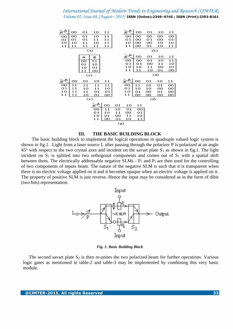
III. THE BASIC BUILDING BLOCK
The basic building block to implement the logical operations in quadruple valued logic system is
shown in fig.1. Light from a laser source L after passing through the polarizer P is polarized at an angle
45o with respect to the two crystal axes and incident on the savart plate S1 as shown in fig.1. The light
incident on S1 is splitted into two orthogonal components and comes out of S1 with a spatial shift
between them. The electrically addressable negative SLMs - P1 and P2 are then used for the controlling
of two components of inputs beam. The nature of the negative SLM is such that it is transparent when
there is no electric voltage applied on it and it becomes opaque when an electric voltage is applied on it.
The property of positive SLM is just reverse. Hence the input may be considered as in the form of dibit
(two bits) representation.
Fig. 1: Basic Building Block
The second savart plate S2 is then re-unites the two polarized beam for further operations. Various
logic gates as mentioned in table-2 and table-3 may be implemented by combining this very basic
module.
International Journal of Modern Trends in Engineering and Research (IJMTER) Volume 02, Issue 08, [August– 2015] ISSN (Online):2349–9745 ; ISSN (Print):2393-8161
@IJMTER-2015, All rights Reserved 34
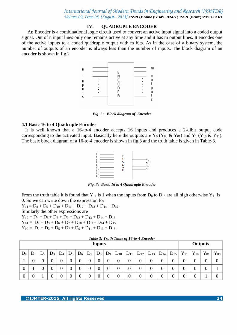
IV. QUADRUPLE ENCODER
An Encoder is a combinational logic circuit used to convert an active input signal into a coded output
signal. Out of n input lines only one remains active at any time and it has m output lines. It encodes one
of the active inputs to a coded quadruple output with m bits. As in the case of a binary system, the
number of outputs of an encoder is always less than the number of inputs. The block diagram of an
encoder is shown in fig.2
Fig. 2: Block diagram of Encoder
4.1 Basic 16 to 4 Quadruple Encoder
It is well known that a 16-to-4 encoder accepts 16 inputs and produces a 2-dibit output code
corresponding to the activated input. Basically here the outputs are Y0 (Y00 & Y01) and Y1 (Y10 & Y11).
The basic block diagram of a 16-to-4 encoder is shown in fig.3 and the truth table is given in Table-3.
Fig. 3: Basic 16 to 4 Quadruple Encoder
From the truth table it is found that Y11 is 1 when the inputs from D8 to D15 are all high otherwise Y11 is
0. So we can write down the expression for
Y11 = D8 + D9 + D10 + D11 + D12 + D13 + D14 + D15
Similarly the other expressions are
Y10 = D4 + D5 + D6 + D7 + D12 + D13 + D14 + D15
Y01 = D2 + D3 + D6 + D7 + D10 + D11+ D14 + D15
Y00 = D1 + D3 + D5 + D7 + D9 + D11 + D13 + D15.
Table 3: Truth Table of 16-to-4 Encoder
Inputs Outputs
D0 D1 D2 D3 D4 D5 D6 D7 D8 D9 D10 D11 D12 D13 D14 D15 Y11 Y10 Y01 Y00
1 0 0 0 0 0 0 0 0 0 0 0 0 0 0 0 0 0 0 0
0 1 0 0 0 0 0 0 0 0 0 0 0 0 0 0 0 0 0 1
0 0 1 0 0 0 0 0 0 0 0 0 0 0 0 0 0 0 1 0
International Journal of Modern Trends in Engineering and Research (IJMTER) Volume 02, Issue 08, [August– 2015] ISSN (Online):2349–9745 ; ISSN (Print):2393-8161
@IJMTER-2015, All rights Reserved 35
0 0 0 1 0 0 0 0 0 0 0 0 0 0 0 0 0 0 1 1
0 0 0 0 1 0 0 0 0 0 0 0 0 0 0 0 0 1 0 0
0 0 0 0 0 1 0 0 0 0 0 0 0 0 0 0 0 1 0 1
0 0 0 0 0 0 1 0 0 0 0 0 0 0 0 0 0 1 1 0
0 0 0 0 0 0 0 1 0 0 0 0 0 0 0 0 0 1 1 1
0 0 0 0 0 0 0 0 1 0 0 0 0 0 0 0 1 0 0 0
0 0 0 0 0 0 0 0 0 1 0 0 0 0 0 0 1 0 0 1
0 0 0 0 0 0 0 0 0 0 1 0 0 0 0 0 1 0 1 0
0 0 0 0 0 0 0 0 0 0 0 1 0 0 0 0 1 0 1 1
0 0 0 0 0 0 0 0 0 0 0 0 1 0 0 0 1 1 0 0
0 0 0 0 0 0 0 0 0 0 0 0 0 1 0 0 1 1 0 1
0 0 0 0 0 0 0 0 0 0 0 0 0 0 1 0 1 1 1 0
0 0 0 0 0 0 0 0 0 0 0 0 0 0 0 1 1 1 1 1
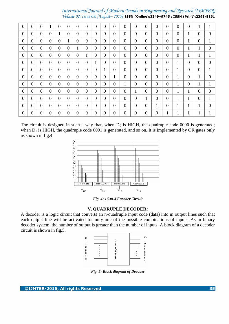
The circuit is designed in such a way that, when D0 is HIGH, the quadruple code 0000 is generated;
when D1 is HIGH, the quadruple code 0001 is generated, and so on. It is implemented by OR gates only
as shown in fig.4.
Fig. 4: 16-to-4 Encoder Circuit
V. QUADRUPLE DECODER:
A decoder is a logic circuit that converts an n-quadruple input code (data) into m output lines such that
each output line will be activated for only one of the possible combinations of inputs. As in binary
decoder system, the number of output is greater than the number of inputs. A block diagram of a decoder
circuit is shown in fig.5.
Fig. 5: Block diagram of Decoder
International Journal of Modern Trends in Engineering and Research (IJMTER) Volume 02, Issue 08, [August– 2015] ISSN (Online):2349–9745 ; ISSN (Print):2393-8161
@IJMTER-2015, All rights Reserved 36
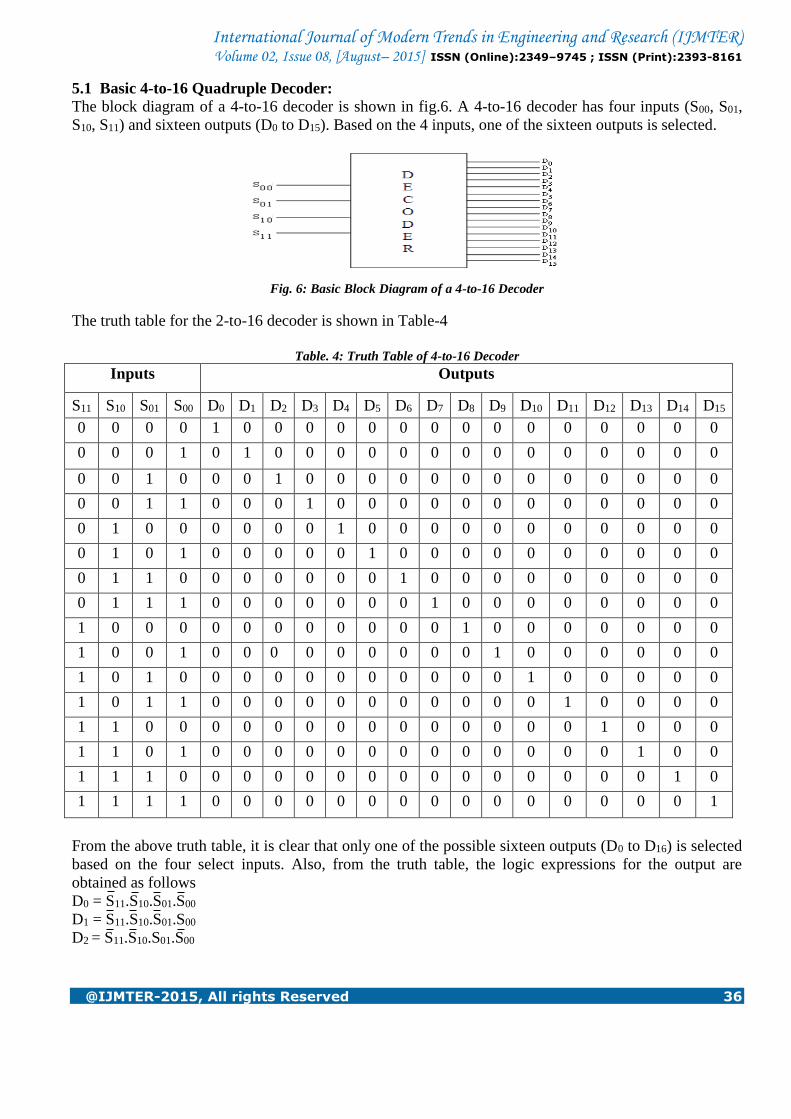
5.1 Basic 4-to-16 Quadruple Decoder:
The block diagram of a 4-to-16 decoder is shown in fig.6. A 4-to-16 decoder has four inputs (S00, S01,
S10, S11) and sixteen outputs (D0 to D15). Based on the 4 inputs, one of the sixteen outputs is selected.
Fig. 6: Basic Block Diagram of a 4-to-16 Decoder
The truth table for the 2-to-16 decoder is shown in Table-4
Table. 4: Truth Table of 4-to-16 Decoder
Inputs Outputs
S11 S10 S01 S00 D0 D1 D2 D3 D4 D5 D6 D7 D8 D9 D10 D11 D12 D13 D14 D15
0 0 0 0 1 0 0 0 0 0 0 0 0 0 0 0 0 0 0 0
0 0 0 1 0 1 0 0 0 0 0 0 0 0 0 0 0 0 0 0
0 0 1 0 0 0 1 0 0 0 0 0 0 0 0 0 0 0 0 0
0 0 1 1 0 0 0 1 0 0 0 0 0 0 0 0 0 0 0 0
0 1 0 0 0 0 0 0 1 0 0 0 0 0 0 0 0 0 0 0
0 1 0 1 0 0 0 0 0 1 0 0 0 0 0 0 0 0 0 0
0 1 1 0 0 0 0 0 0 0 1 0 0 0 0 0 0 0 0 0
0 1 1 1 0 0 0 0 0 0 0 1 0 0 0 0 0 0 0 0
1 0 0 0 0 0 0 0 0 0 0 0 1 0 0 0 0 0 0 0
1 0 0 1 0 0 0 0 0 0 0 0 0 1 0 0 0 0 0 0
1 0 1 0 0 0 0 0 0 0 0 0 0 0 1 0 0 0 0 0
1 0 1 1 0 0 0 0 0 0 0 0 0 0 0 1 0 0 0 0
1 1 0 0 0 0 0 0 0 0 0 0 0 0 0 0 1 0 0 0
1 1 0 1 0 0 0 0 0 0 0 0 0 0 0 0 0 1 0 0
1 1 1 0 0 0 0 0 0 0 0 0 0 0 0 0 0 0 1 0
1 1 1 1 0 0 0 0 0 0 0 0 0 0 0 0 0 0 0 1
From the above truth table, it is clear that only one of the possible sixteen outputs (D0 to D16) is selected
based on the four select inputs. Also, from the truth table, the logic expressions for the output are
obtained as follows
D0 = S11.S10.S01.S00
D1 = S11.S10.S01.S00
D2 = S11.S10.S01.S00
International Journal of Modern Trends in Engineering and Research (IJMTER) Volume 02, Issue 08, [August– 2015] ISSN (Online):2349–9745 ; ISSN (Print):2393-8161
@IJMTER-2015, All rights Reserved 37
D3 = S11.S10.S01.S00
D4 = S11.S10.S01.S00
D5 = S11.S10.S01.S00
D6 = S11.S10.S01.S00
D7 = S11.S10.S01.S00
D8 = S11.S10.S01.S00
D9 = S11.S10.S01.S00
D10 = S11.S10.S01.S00
D11 = S11.S10.S01.S00
D12 = S11.S10.S01.S00
D13 = S11.S10.S01.S00
D14 = S11.S10.S01.S00
D15 = S11.S10.S01.S00
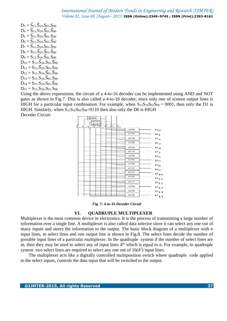
Using the above expressions, the circuit of a 4-to-16 decoder can be implemented using AND and NOT
gates as shown in Fig.7. This is also called a 4-to-16 decoder, since only one of sixteen output lines is
HIGH for a particular input combination. For example, when S11S10S01S00 = 0001, then only the D1 is
HIGH. Similarly, when S11S10S01S00=0110 then also only the D6 is HIGH
Decoder Circuit:
Fig. 7: 4-to-16 Decoder Circuit
VI. QUADRUPLE MULTIPLEXER
Multiplexer is the most common device in electronics. It is the process of transmitting a large number of
information over a single line. A multiplexer is also called data selector since it can select any one out of
many inputs and steers the information to the output. The basic block diagram of a multiplexer with n
input lines, m select lines and one output line is shown in Fig.8. The select lines decide the number of
possible input lines of a particular multiplexer. In the quadruple system if the number of select lines are
m, then they may be used to select any of input lines 4m which is equal to n. For example, in quadruple
system two select lines are required to select any one out of 16(42) input lines.
The multiplexer acts like a digitally controlled multiposition switch where quadruple code applied
to the select inputs, controls the data input that will be switched to the output.
International Journal of Modern Trends in Engineering and Research (IJMTER) Volume 02, Issue 08, [August– 2015] ISSN (Online):2349–9745 ; ISSN (Print):2393-8161
@IJMTER-2015, All rights Reserved 38
Fig. 8: Block Diagram of Multiplexer
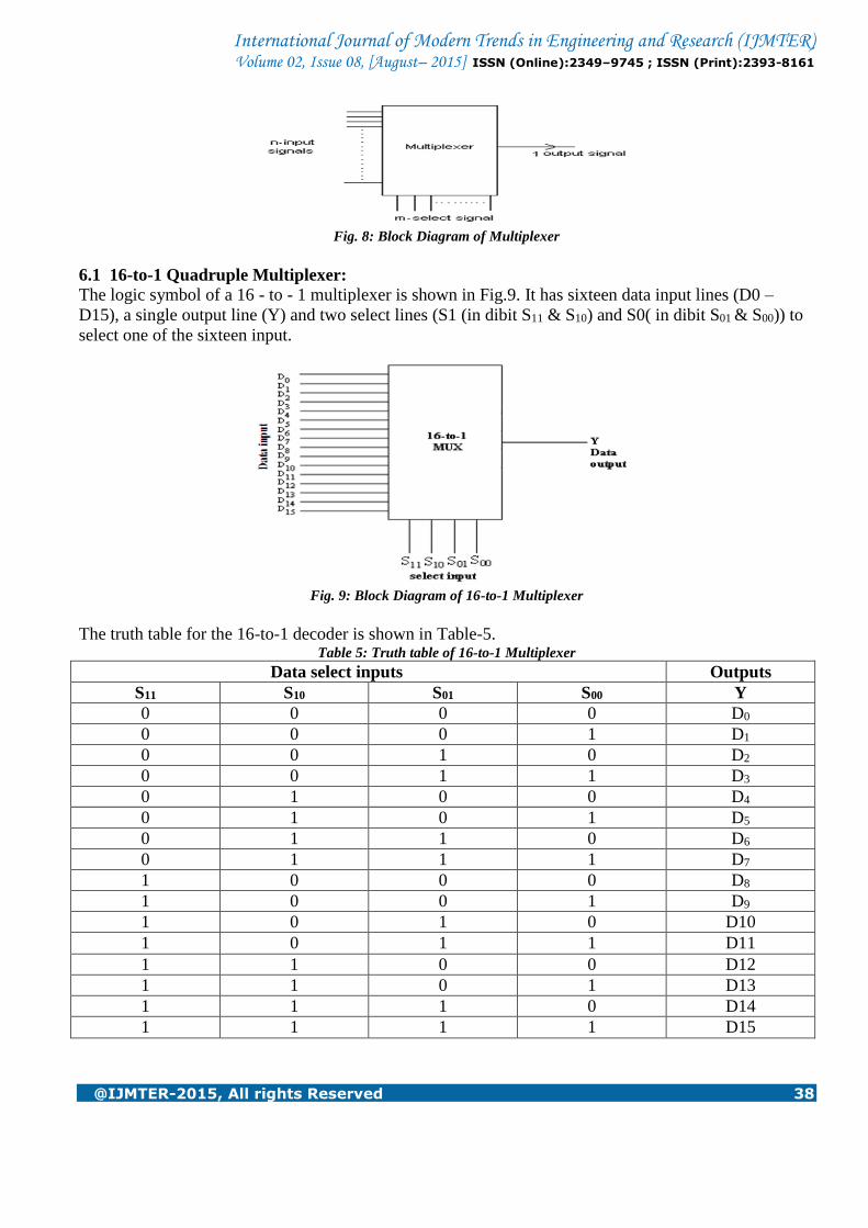
6.1 16-to-1 Quadruple Multiplexer: The logic symbol of a 16 - to - 1 multiplexer is shown in Fig.9. It has sixteen data input lines (D0 –
D15), a single output line (Y) and two select lines (S1 (in dibit S11 & S10) and S0( in dibit S01 & S00)) to
select one of the sixteen input.
Fig. 9: Block Diagram of 16-to-1 Multiplexer
The truth table for the 16-to-1 decoder is shown in Table-5. Table 5: Truth table of 16-to-1 Multiplexer
Data select inputs Outputs
S11 S10 S01 S00 Y
0 0 0 0 D0
0 0 0 1 D1
0 0 1 0 D2
0 0 1 1 D3
0 1 0 0 D4
0 1 0 1 D5
0 1 1 0 D6
0 1 1 1 D7
1 0 0 0 D8
1 0 0 1 D9
1 0 1 0 D10
1 0 1 1 D11
1 1 0 0 D12
1 1 0 1 D13
1 1 1 0 D14
1 1 1 1 D15
International Journal of Modern Trends in Engineering and Research (IJMTER) Volume 02, Issue 08, [August– 2015] ISSN (Online):2349–9745 ; ISSN (Print):2393-8161
@IJMTER-2015, All rights Reserved 39
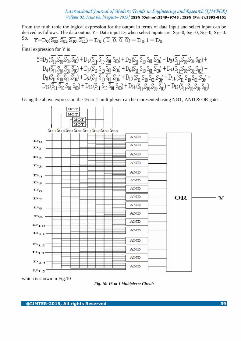
From the truth table the logical expression for the output in terms of data input and select input can be
derived as follows. The data output Y= Data input D0 when select inputs are S00=0, S01=0, S10=0, S11=0.
So,
,
Final expression for Y is
Using the above expression the 16-to-1 multiplexer can be represented using NOT, AND & OR gates
which is shown in Fig.10 Fig. 10: 16-to-1 Multiplexer Circuit
International Journal of Modern Trends in Engineering and Research (IJMTER) Volume 02, Issue 08, [August– 2015] ISSN (Online):2349–9745 ; ISSN (Print):2393-8161
@IJMTER-2015, All rights Reserved 40
VII. QUADRUPLE DEMULTIPLEXER
Demultiplexing is the process of taking information from one input and transmitting the same over one
of several outputs. A demultiplexer is a logic circuit that receives information on a single input and
transmits the same over one of the several (4n) output lines. The block diagram of a demultiplexer which
is opposite to a multiplexer in its operation is shown in Fig 11. The circuit has one input signal, m select
signals and n output signals. The select input determines to which output the data input will be
connected. As the serial data is changed to parallel data, i.e. the input causes to appear on one of the n
output lines, the demultiplexer is also called a distributor or a serial-to- parallel converter.
Fig. 11: Basic block diagram of Demultiplexer
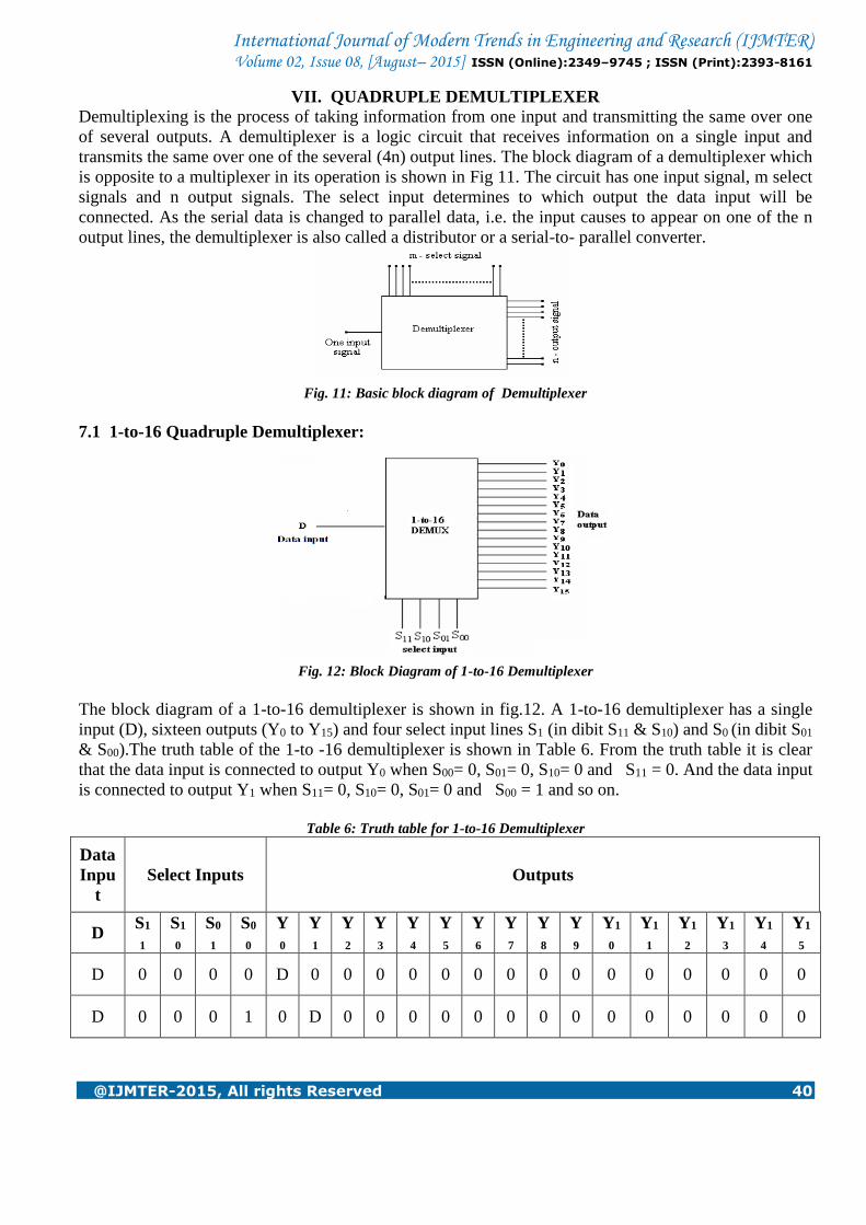
7.1 1-to-16 Quadruple Demultiplexer:
Fig. 12: Block Diagram of 1-to-16 Demultiplexer
The block diagram of a 1-to-16 demultiplexer is shown in fig.12. A 1-to-16 demultiplexer has a single
input (D), sixteen outputs (Y0 to Y15) and four select input lines S1 (in dibit S11 & S10) and S0 (in dibit S01
& S00).The truth table of the 1-to -16 demultiplexer is shown in Table 6. From the truth table it is clear
that the data input is connected to output Y0 when S00= 0, S01= 0, S10= 0 and S11 = 0. And the data input
is connected to output Y1 when S11= 0, S10= 0, S01= 0 and S00 = 1 and so on.
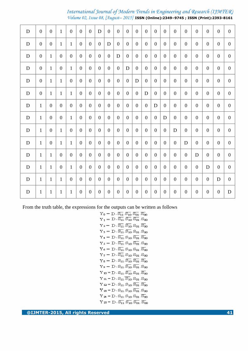
Table 6: Truth table for 1-to-16 Demultiplexer
Data
Inpu
t
Select Inputs Outputs
D S1
1
S1
0
S0
1
S0
0
Y
0
Y
1
Y
2
Y
3
Y
4
Y
5
Y
6
Y
7
Y
8
Y
9
Y1
0
Y1
1
Y1
2
Y1
3
Y1
4
Y1
5
D 0 0 0 0 D 0 0 0 0 0 0 0 0 0 0 0 0 0 0 0
D 0 0 0 1 0 D 0 0 0 0 0 0 0 0 0 0 0 0 0 0
International Journal of Modern Trends in Engineering and Research (IJMTER) Volume 02, Issue 08, [August– 2015] ISSN (Online):2349–9745 ; ISSN (Print):2393-8161
@IJMTER-2015, All rights Reserved 41
D 0 0 1 0 0 0 D 0 0 0 0 0 0 0 0 0 0 0 0 0
D 0 0 1 1 0 0 0 D 0 0 0 0 0 0 0 0 0 0 0 0
D 0 1 0 0 0 0 0 0 D 0 0 0 0 0 0 0 0 0 0 0
D 0 1 0 1 0 0 0 0 0 D 0 0 0 0 0 0 0 0 0 0
D 0 1 1 0 0 0 0 0 0 0 D 0 0 0 0 0 0 0 0 0
D 0 1 1 1 0 0 0 0 0 0 0 D 0 0 0 0 0 0 0 0
D 1 0 0 0 0 0 0 0 0 0 0 0 D 0 0 0 0 0 0 0
D 1 0 0 1 0 0 0 0 0 0 0 0 0 D 0 0 0 0 0 0
D 1 0 1 0 0 0 0 0 0 0 0 0 0 0 D 0 0 0 0 0
D 1 0 1 1 0 0 0 0 0 0 0 0 0 0 0 D 0 0 0 0
D 1 1 0 0 0 0 0 0 0 0 0 0 0 0 0 0 D 0 0 0
D 1 1 0 1 0 0 0 0 0 0 0 0 0 0 0 0 0 D 0 0
D 1 1 1 0 0 0 0 0 0 0 0 0 0 0 0 0 0 0 D 0
D 1 1 1 1 0 0 0 0 0 0 0 0 0 0 0 0 0 0 0 D
From the truth table, the expressions for the outputs can be written as follows
International Journal of Modern Trends in Engineering and Research (IJMTER) Volume 02, Issue 08, [August– 2015] ISSN (Online):2349–9745 ; ISSN (Print):2393-8161
@IJMTER-2015, All rights Reserved 42
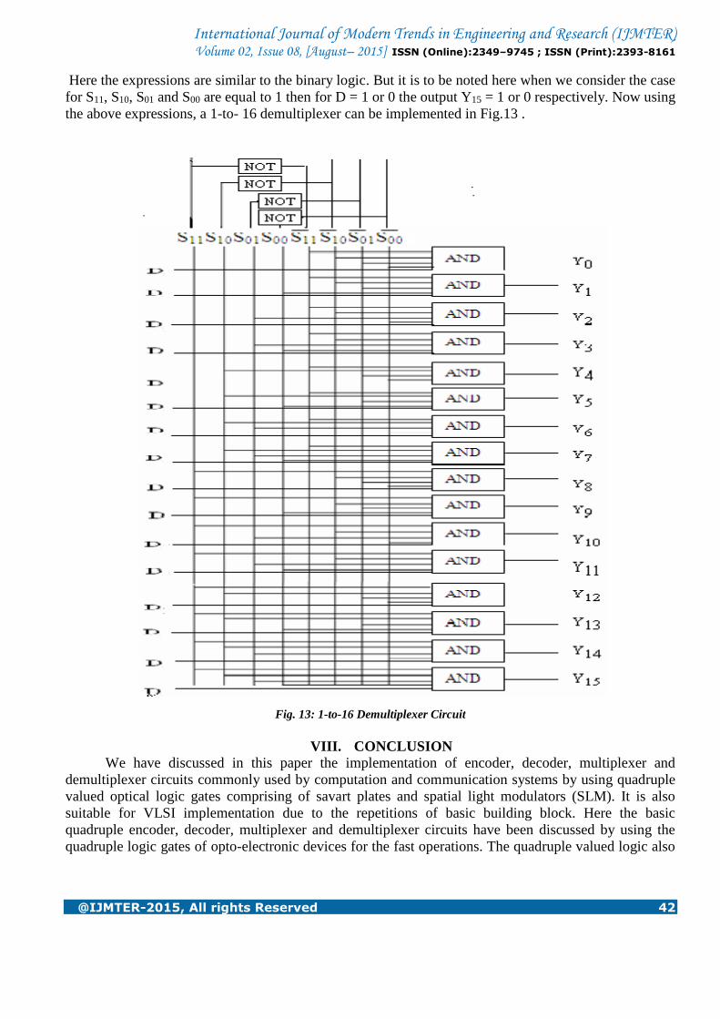
Here the expressions are similar to the binary logic. But it is to be noted here when we consider the case
for S11, S10, S01 and S00 are equal to 1 then for D = 1 or 0 the output Y15 = 1 or 0 respectively. Now using
the above expressions, a 1-to- 16 demultiplexer can be implemented in Fig.13 .
Fig. 13: 1-to-16 Demultiplexer Circuit
VIII. CONCLUSION
We have discussed in this paper the implementation of encoder, decoder, multiplexer and
demultiplexer circuits commonly used by computation and communication systems by using quadruple
valued optical logic gates comprising of savart plates and spatial light modulators (SLM). It is also
suitable for VLSI implementation due to the repetitions of basic building block. Here the basic
quadruple encoder, decoder, multiplexer and demultiplexer circuits have been discussed by using the
quadruple logic gates of opto-electronic devices for the fast operations. The quadruple valued logic also
International Journal of Modern Trends in Engineering and Research (IJMTER) Volume 02, Issue 08, [August– 2015] ISSN (Online):2349–9745 ; ISSN (Print):2393-8161
@IJMTER-2015, All rights Reserved 43
find its applications in gray image processing, cellular automata, fuzzy logic systems, fractals and other
emerging areas where the fast operations are needed.
REFERENCES [1] A.W.Lohmann,“Polarization and optical logic,”Appl.Opt.,vol.25,pp.1594-1597, 1986.
[2] A.Avizienis,“Signed-Digit Number Representation for Fast Parallel Arithmetic,” IRE Trans. Electron. & Comp. EC-
10, pp. 389-400, 1961.
[3] B.L. Drake, R.P.Bocker, M.E.Lasher, R.H.Patterson and W.J. Miceli, “Photonic computing using the modified-signed-
digit number representation,” Opt. Eng., vol.25, pp.38-43,1986.
[4] R.P.Bocker, B.L.Drake, M.E.Lasher and T.B. Henderson, “Modified signed-digit addition and subtraction using
optical symbolic substitution,” Appl.Opt., vol. 25(15), pp.2456-2457, 1986.
[5] A.K.Cherri and M.A.Karim, “Modified signed digit arithmetic using an efficient symbolic substitution,” Appl.Opt.,
vol.27,no.18,pp.3824-3827, 1988.
[6] A.K.Datta,A.Basuray and S.Mukhopadhyay,“Arithmetic operations in optical computations using a modified trinary
number system,”Optics Letters, vol.14, pp.426-428, 1989.
[7] A. K. Cherri, "Designs of Optoelectronic Trinary Signed-Digit Multiplication by use of Joint Spatial Encodings and
Optical Correlation," Appl. Opt.,vol.38, pp.828-837,1999.
[8] M.S.Alam, M.A.Karim, A.A.S.Awwal and J.J.Westerkamp, “Optical processing based on conditional higher-order
trinary modified signed-digit symbolic substitution”, Applied Optics,vol.31, issue 26, pp.5614-5621, September 10,
1992.
[9] R.S.Fyath, A.A.W.Alsaffar and M.S. Alam, "Optical two-step modified signed-digit addition based on binary logic
gates", Optics Communications, vol.208, no.4, pp. 263-273, 2002.
[10] R. S. Fyath, A. A. W. Alsaffar and M. S. Alam,“Nonrecoded trinary signed-digit multiplication based on digit
grouping and pixel assignment”, Optics Communications,vol.230, issue 1-3, pp.35-44, 2004.
[11] A.Basuray, S.Mukhopadhyay, Hirak K.Ghosh and A.K.Dutta,“A tristate optical logic system”, Optics Comm.,vol.85,
pp 167 –170, 1991.
[12] S. Lin and I.Kumazawa, “Optical fuzzy image processing based on shadow casting”, Optics Communications, vol. 94,
pp.397-405, 1992.
[13] J.Łukasiewicz:“O logice trojwartosciowej,” Ruch Filozoficny, vol.5, pp.169- 171, 1920. [English translation in:
Łukasiewicz (1970).]
[14] J.Lukasiewicz: Aristotles Syllogistic from the stand point of modern formal logic, Oxford, London, 1951.
[15] J.Lukasiewicz, “Selected Works”, L. Borkowski(ed.), North-Holland Publ. Comp., Amsterdam and PWN, Warsaw,
1970.
[16] R.Wojcicki and G.Malinowski,ed.: Selected Papers on Łukasiewicz Sentential Calculi. Ossolineum, Wroclaw, 1977.
[17] J.Lukasiewicz and A.Tarski. Untersuchungen uber den Aussagenkalkul. Comptes rendus de la Societe des Sciences et
des Lettres de Varsovie,23(iii):30-50, 1930.
[18] U.Kalay, M.A.Perkowski and D.V.Hall,“Highly testable Boolean ring logic circuits”, ISMVL 1999, pp.268-274,
1999.
[19] Amal K.Ghosh, P.Pal Choudhury and A.Basuray, “Modified Trinary Optical Logic Gates and their Applications
in Optical Computation”, presented in the Third International Conference on CISSE 2007, IEEE, University of
Bridgeport, 3-12 December 2007 (2007) and published in the proceeding on Innovations and Advanced
Techniques in Systems, Computing Sciences and Software (Springer, 2008) pp. 87-92 (2008).
[20] Amal K. Ghosh,“Parity Generator and Parity Checker in the Modified Trinary Number system using Savart Plate
and Spatial Light Modulator”, has been published in Optoelectronics
Letters,Volume 6, No.5, pp.325-327, September,2010.
[21] Amal K. Ghosh and Amitabha Basuray, “ Binary to Modified Trinary Number System Conversion and Vice-
Versa for Optical Super Computing ”, Natural Computing, Volume 9, No.4, pp.917-934, [DOI 10.1007/s11047-009-
9166-4 / November 2009], Special issue "Optical Supercomputing", December 2010.
[22] Amal K. Ghosh, Animesh Bhattacharya, Moumita Raul and Amitabha Basuray,“Trinary Arithmetic and Logic unit
(TALU) using savart plate and spatial light modulator (SLM) suitable for optical computation in multivalued
logic” , Optics & Laser Technology, Volume 44, Issue 5, July 2012, Pages 1583-1592.
[23] Amal K. Ghosh, P. Pal Choudhury and A. Basuray, “Chaotic Fractals with Multivalued Logic in Cellular
Automata”, CISSE 2006, IEEE, University of Bridgeport, Innovations and Advanced Techniques in Computer and
Information Sciences and Engineering, pp.77-82 ©2007 Springer (2007)..
[24] Amal K. Ghosh, Animesh Bhattacharya, Amitabha Basuray “Quadruple - Valued Logic System Using Savart
Plate and Spatial Light Modulator (SLM) and It's Applications ” Journal of Computational Electronics ,
Volume 11, Issue 4, pp 405- 413, December 2012, [DOI 10.1007/s10825-012-0420-0]


![MA251 Computer Organization and Architecture [3-0 … Computer Organization and Architecture [3-0-0-6] Lecture 5: Decoder, Demultiplexer, Encoder, and Multiplexer.. Spring 2011 Partha](https://img.dokumen.tips/doc/110x75/5afebecb7f8b9a994d8f6d58/ma251-computer-organization-and-architecture-3-0-computer-organization-and.jpg)