Embed Size (px)
Citation preview
Empirical Model Based Variability Analysis of
Terminal Currents of MOSFET of a 65nm SRAM
Cell in Process-Voltage-Temperature (PVT) Space
Malleshaiah G. V, Department of Electronics and Communication
Engineering, Eastpoint College of Engineering
for Women (EPCEW), Bangalore, India
H. C. Srinivasaiah, Department of Telecommunication Engineering,
Dayananda Sagar College of Engineering,
Bangalore, India
Parameshwara. M. C, Department of Electronics and Communication
Engineering, Vemana Institute of Technology,
Bangalore, India.
Shashidhara. K. S, Department of Electronics and Communication
Engineering, NMIT, Bangalore,
India.
Abstract—Three dimension (3D) process/device simulation and
optimization of MOS transistor of 65nm SRAM cell is done using
implant ‘dose matching’ technique saving optimization time and
computational resources. For this optimized transistor,
source/drain (s/d) junction leakage (to substrate) current Ib, drain
current Id, and gate leakage current Ig are empirically modeled in
terms of five “process-voltage-temperature (PVT) parameters
such as gate length Lg, device operating temperature ‘tempr’,
substrate bias Vb, drain bias Vd, and gate bias Vg using standard
3-level Design of Experiment technique over the entire bias range
from 0V to 1.2V, in two steps (DoE). The second order empirical
models for the responses: Ib, Id, and Ig are used to estimate their
variability in terms of variability of the PVT parameters. The 3
variability of electrical variables: Vb, Vd, and Vg are seen highly
significant compared to the 3 variability in nonelectrical
variables: Lg and tempr. Among the 3 bias voltages, Vg ranks
first with a contribution of 44.78% on Id, 46% on Ib, and 22.94%
on Ig; Vd ranks 2nd, with a contribution of 39.76% on Id, 44.34%
on Ib, and 23% on Ig; and Vb rank 3rd with a contribution of 10%
on Id, 4.3% on Ib, and 23.2% on Ig. Among the nonelectrical
variables, tempr (over 270-330oK range about mean 300oK)
contributes: 1.97% on Id, 2.8% on Ib, and 16.41% on Ig; the
contribution of Lg (over 58.5-71.5nm range about mean 65nm) is:
3.43% on Id, 2.54% on Ib, and 14.43% on Ig. These contributions
are in the vicinity of ‘threshold’, ‘subthreshold’ and ‘linear’
region. A similar estimation is done in ‘above threshold’ and
‘saturation’ region as discussed further in this paper.
Keywords: Process sensitivity, Bias sensitivity, Temperature
sensitivity, Manufacturing process modeling, Gate leakage,
Substrate currents, and Statistical variability.
I. INTRODUCTION
Two issues of integrated circuit (IC) industry are increasing
of yield and improving product quality, which are
simultaneously achieved at lowest production cost [1]. This
goal is met using advanced process control (APC) and
monitoring technologies. The goal of process control is to
achieve minimum variability in the process outputs which
in turn depend on variability in process parameters (PPs). The
APC involves highly adaptive control technique based on
virtual metrology (VM). In VM based APC, the process is
monitored based on process outputs calculated using process
based predictive models (PMs) for accurate process
conjecturing [2, 3]. Modern process control is data driven,
wherein controllers are trained, using metrology data or some
estimated data and process recipes [3, 4, 5]; this training is a
continuous process.
In modern deep submicron (DSM) devices, random discrete
dopants (RDD), is a dominant source of statistical variability,
due to the discrete nature of charge. Apart from RDD
variability, fluctuations in poly line edge roughness, poly-Si
granularity, oxide thickness, interface trapped charges, etc.,
will also contribute to (intrinsic) variability [6]. The total
variability is the combined effect of process variability and
intrinsic variability. The total variability increases with
miniaturization of MOSFET devices [7].
In this paper, PMs are experimentally derived for 3 terminal
currents such as s/d junction leakage current Ib, drain current
Id, and gate leakage current Ig of a 65nm NMOSFET of a
0.594μm2, SRAM cell [8] in terms of 5 PVT parameters such
as gate length Lg, device operating temperature ‘tempr’,
substrate bias Vb, drain bias Vd, and gate bias Vg using
standard 3-level face centered central composite (FCCC) DoE.
The modeling is done through 3D process/device simulation
and optimization of this 65nm NMOSFET, to capture second
order effects [9] accurately. These PMs are used to predict
variability [10] in Ib, Id, and Ig in terms of variability in Lg,
tempr, Vb, Vd, and Vg.. In deriving these PMs, novel 3D device
design/optimization technique (discussed later) is followed,
saving significant computation time and resources.
Section II of this paper present basic concept of modeling.
Section III discusses a heuristic called ‘dose matching’
technique to reduce the 3D process/device simulation and
optimization time. This technique is used to optimize 3D
1302
Vol. 3 Issue 3, March - 2014
International Journal of Engineering Research & Technology (IJERT)
IJERT
IJERT
ISSN: 2278-0181
www.ijert.orgIJERTV3IS031505
devices’ implant doses against reference 2D devices’
analytical implant profiles. In section IV, second order
empirical models (EMs) for 3 responses Ib, Id, and Ig are
obtained in terms of 5 PVT parameters Lg, ‘tempr’, Vb, Vd,
and Vg. Section V discusses statistical analysis of Ib, Id, and Ig
using their EMs (acronym EM, and PM are synonymously
used). In section VI, we conclude with the discussion on the
results.
II. AN OVERVIEW OF MODELING METHODOLOGY
Fig. 1 gives relationship between response vector rl in terms
of PP vector xn, n=1, 2, …k. This relationship between vector r
and x can be written as:
𝑟𝑙 = 𝑓 (𝑥1 , 𝑥2,… . , 𝑥𝑘) for l=1, 2, … m. (1)
Fig. 1: General relationship between input PP ‘x’ and the process output
(response) variable ‘r’ in a manufacturing process.
Generally f is second order polynomial relation [11, 12],
given as:
𝑟𝑙 = 𝑏0 + 𝑏𝑖 𝑥𝑖 5𝑖=1 + 𝑏𝑖𝑖 𝑥𝑖
25𝑖=1 + 𝑏𝑖𝑗 𝑥𝑖 𝑥𝑗
5𝑗=𝑖+1
5𝑖=1 (2)
for l=1, 2, … m, m=3 for 3 responses Ib, Id, and Ig; k=5 for 5
PVT parameters: Lg, tempr, Vb, Vd, and Vg, where b0 is a
constant term, bii are coefficients of quadratic term, and bij are
the coefficients for cross coupled terms.
Eqn. 2 is obtained using 3-level FCCC DoE. The FCCC
DoE needs 43 (25=32 factorial points, 2×5=10 axial points and
one point at center of design, adding to 43) experiments, for 5
factors; each experiment is a 3D process/device simulation; 21
coefficients of Eqn. 2 are elements of columns of matrix B,
obtained from DoE data, given as:
𝐵 = 𝑋𝑇𝑋 −1𝑋𝑇𝑟 (3)
where B=[B1,B2,B3], is a 21×3 dimension coefficient matrix,
r=[r1, r2, r3] (=[Ib, Id, Ig]), is a 43×3 dimension response
matrix, X is a 43×21 dimension design matrix for 3-level
FCCC DoE for 5 factors; 𝐵1 = 𝑋𝑇𝑋 −1𝑋𝑇𝑟1, 𝐵2 = 𝑋𝑇𝑋 −1𝑋𝑇𝑟2, and 𝐵3 = 𝑋𝑇𝑋 −1𝑋𝑇𝑟3 are coefficient vectors
whose elements are b0, bi, and bij in Eqn. 2. The 3 responses Ib,
Id, and Ig are extracted from 43, 3D process/device simulations.
III. DEVICE DESIGN METHODOLOGY FOR 3D STRUCTURE
The dose matching technique [13] requires calculation of
implant doses for 3D nominal device from optimized
analytical implant profile for 2D reference device. In this
work, construction and optimization of 2D reference device is
done by a simple script to define the boundary, doping
profiles, and meshing criteria, etc., using a device editor tool.
This takes a few seconds to obtain meshed 2D device. This
reference 2D, 65nm device is optimized to match its
characteristics with ITRS [14] specification.
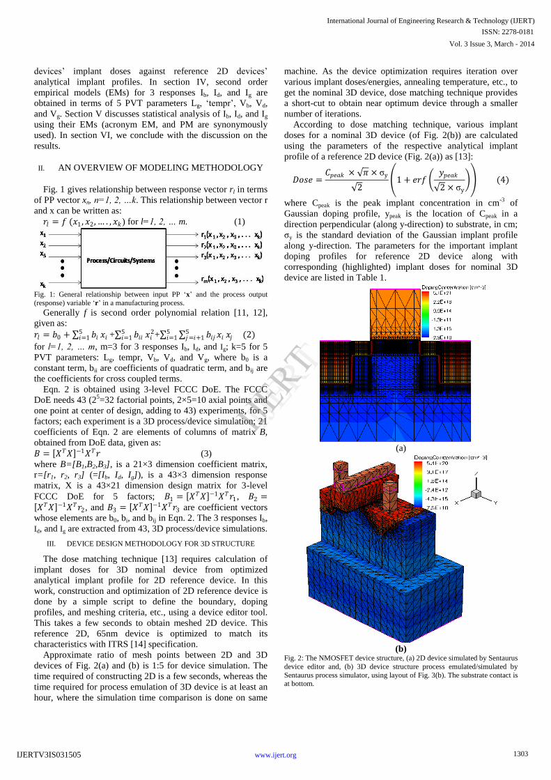
Approximate ratio of mesh points between 2D and 3D
devices of Fig. 2(a) and (b) is 1:5 for device simulation. The
time required of constructing 2D is a few seconds, whereas the
time required for process emulation of 3D device is at least an
hour, where the simulation time comparison is done on same
machine. As the device optimization requires iteration over
various implant doses/energies, annealing temperature, etc., to
get the nominal 3D device, dose matching technique provides
a short-cut to obtain near optimum device through a smaller
number of iterations.
According to dose matching technique, various implant
doses for a nominal 3D device (of Fig. 2(b)) are calculated
using the parameters of the respective analytical implant
profile of a reference 2D device (Fig. 2(a)) as [13]:
𝐷𝑜𝑠𝑒 =𝐶𝑝𝑒𝑎𝑘 × 𝜋 × σy
2 1 + 𝑒𝑟𝑓
𝑦𝑝𝑒𝑎𝑘
2 × σy
(4)
where Cpeak is the peak implant concentration in cm-3
of
Gaussian doping profile, ypeak is the location of Cpeak in a
direction perpendicular (along y-direction) to substrate, in cm;
σy is the standard deviation of the Gaussian implant profile
along y-direction. The parameters for the important implant
doping profiles for reference 2D device along with
corresponding (highlighted) implant doses for nominal 3D
device are listed in Table 1.
(a)
(b)
Fig. 2: The NMOSFET device structure, (a) 2D device simulated by Sentaurus
device editor and, (b) 3D device structure process emulated/simulated by
Sentaurus process simulator, using layout of Fig. 3(b). The substrate contact is at bottom.
1303
Vol. 3 Issue 3, March - 2014
International Journal of Engineering Research & Technology (IJERT)
IJERT
IJERT
ISSN: 2278-0181
www.ijert.orgIJERTV3IS031505

TABLE 1: 2D IMPLANT PROFILE PARAMETERS AND THE CORRESPONDING
(CALCULATED) DOSES FOR 3D PROCESS SIMULATION/EMULATION.
Parameters
of analytical
implant
profile
deep s/d
shallow
s/d (or
LDD)
SSRC halo
cpeak (cm-3) 5.0×10
21 1.0×10
20 1.0×10
18 2.0×10
18
σy (cm) 1.4×10⁻⁶
5.0×10⁻⁷
5.0×10⁻⁶
5.0×10⁻⁶
ypeak (cm) 0 5.0×10⁻⁷
1.0×10⁻⁶
3.0×10⁻⁶
Dose (cm-2
) 8.8×10¹⁵
1.0×10¹⁴
1.3×10¹³
2.3×10¹³
In the process emulation steps for 3D NMOS device (Fig.
2(b)) is followed from the reference [8]. The main implant
parameter values give in Table 1. The main implants that
characterize the device performance in DSM regime are deep
s/d implant, low drain doping (LDD) implant, pocket halo
implant, and super steep retrograde channel (SSRC) implant.
In order to activate deep s/d, and LDD/halo implant species, 2
step annealing is performed; one at 1000oC for 15 sec to
activate deep s/d implant species, and another at 1000oC for 3
sec to activate LDD/halo implant species. In order to control
lateral straggle of LDD implant, a nitride spacer of 5nm
thickness is deposited isotropically over poly-gate during this
implant process step [15] to get s/d and gate overlap of 3D
device identical to that of 2D device. Halo and SSRC implants
are used to control short channel effect (SCE) [9].
Word ‘process emulation’ is used here, as some of the
structural parameters are process emulated by Sentaurus
TCAD tool’s 3D geometric operation capability [13], which is
computationlly economical. The process steps such as
implantation, annealing, etc., are simulated, and the process
steps such as etch, deposition, etc., are emulated.
Fig. 3(a) shows 6T SRAM cell circuit and Fig. 3(b), the
corresponding layout with cell area=0.594μm2. Fig. 3(b) is a
simplified layout to highlight the necessary details for the
mask driven process simulation/emulation. This layout
encompasses the simulation domain of 3D NMOSFET (M1)
device marked and labeled by a rectangle. This rectangle
contains all the layers that are required to simulate/emulate the
3D structure of Fig. 2(b). The structure of Fig. 2(b)
representing transistor M1 of SRAM cell is simplified by
removing (200nm) trench oxide and interlayer dielectric (ILD)
to save mesh points for device simulation. In Fig. 2, gate stack
consists of 15Å of SiO2, over which a 65nm thick polysilicon,
deposited. On top of polysilicon, copper contact is added. In
the current view the boundaries of 15Å SiO2 gate dielectric is
not noticeable, as it is extremely thin compared to other
thicknesses.
M4
M2
VDD
GND
Word line
Bit line Bit-bar line
M3
M1
M5
M6
Q QB
(a)
M1
22l
30l
l=Lg/2 Area=0.594 Sq. Micron
M3
M5
M2M4
M6
PMOS Simulation Domain
NMOS Simulation Domain
Outer Rectangle is the SRAM simulation domain
(b)
Fig. 3: A 6T SRAM cell (a) circuit schematic, (b) simplified view of layout
used for 3D process emulation of SRAM cell/circuit of Fig. 3(a).
Vg=1.2V
Vg=0.9V
Vg=0.6V
Vg=0.3V
Vd=1.2V
Vd=50mV
Fig. 4: The overlapped I-V curves of reference 2D device and the calibrated 3D device (M1 in Fig. 2). Important device characteristics of 2D and 3D
devices match with error less than 20%. The calibrated 3D device is superior
compared to the reference 2D device. All the currents are simulated with 120nm gate width.
The Id-Vd and Id-Vg curves of both reference 2D and
nominal 3D devices of Fig. 2 are shown overlaid in Fig. 4. The
reference 2D device of Fig. 2(a) is optimized for 1mA/μm
drive current in saturation region of operation at 1.2V of
supply (Vdd). The dose matched nominal 3D device is superior
to reference 2D device by over 17% in Id and 15% in Gm, in
saturation region both devices’ width Wg=120nm. This
difference is attributed to a more realistic doping distribution
1304
Vol. 3 Issue 3, March - 2014
International Journal of Engineering Research & Technology (IJERT)
IJERT
IJERT
ISSN: 2278-0181
www.ijert.orgIJERTV3IS031505
and slightly more s/d gate overlap in the case of nominal 3D
device due to annealing, as compared to reference 2D device.
In Table 2 important device parameters extracted for
devices of Fig. 2 are tabulated for comparison in both linear
and saturation region. The extracted threshold voltage is the
constant current Vt=Vg at Id=40nA×(Wg/Lg), with Wg=120nm
and Lg=65nm. The notation in Table 2 is as follows: Vt is the
threshold voltage, DIBL is drain induced barrier lowering, SS
is the subthreshold slope, Gm is the device transconductance, Id
is the drain current. The device parameter suffixes are
interpreted as follows: ‘sat’ is saturation region, ‘lin’ is linear
region, ‘drive’ is on state (at Vg=1.2V), and ‘leak’ is the
leakage (at Vg=0V). For e.g. ‘Idsatdrive’ is the on state saturation
region drain current, Idsatleak is the leakage current in the
saturation region, etc. The linear and saturation region curves
are simulated at Vdd=50mV and 1.2V respectively. During the
device simulation of the 2D and 3D device structures, various
physical models to account for second order effects in 65nm
devices are used. Models to account for hot carriers, channel
mobility degradation, tunneling through gate and junctions,
channel carrier quantization, lattice temperature effect, etc.,
are used. Donor/acceptor trap density of 5×10¹⁰
/cm2, at
Si/SiO2 interface is used during device simulation.
TABLE 2: COMPARISON OF REFERENCE 2D AND NOMINAL 3D 65nm NMOSFET
DEVICE PERFORMANCE IN LINEAR AND SATURATION REGION, WITH EQUAL
DEVICE WIDTHS (=120nm).
Device Parameters 2D Structure 3D Structure
Vtsat (V) 0.2 0.09
Vtlin (V) 0.25 0.13
DIBL (mV/V) 43.19 35.01
SSsat (mV/dec.) 88.65 84.81
SSlin (mV/dec.) 77.72 70.52
Gmsat (mS/120nm) 158.93 177.98
Gmlin (mS/120nm) 21.21 24.38
Idsatdrive (mA/120nm) 0.12 0.14
Idsatleak (nA/120nm) 10.76 5.27
Idlindrive (mA/120nm) 0.01 0.02
Idlinleak (nA/120nm) 0.04 1.34
IV. MODELING OF DEVICE TERMINAL CURRENTS
To empirically model the 3 terminal currents Ib, Id, and Ig of
nominal 3D NMOSFET device (Fig. 2(b)), standard FCCC
DoE for 5 factors (PPs) is used, which requires 43
process/device simulations (section II). Three responses: Ib, Id,
and Ig are measured for all the 43 process/device simulations
and tabulated in a spreadsheet.
As MOSFET devices are highly nonlinear over complete
bias range (from 0V to 1.2V) over the 3 terminals: substrate,
drain and gate, (at source voltage Vs=0V), 2 models for each
response variables Ib, Id, and Ig are fitted using FCCC DoE
data, twice corresponding to 2 regions defined in Table 3.
TABLE 3: 3-LEVELS FOR FCCC DoE OVER 2 BIAS RANGES TO CAPTURE HIGH
NONLINEARITY.
In the vicinity of threshold/subthreshold and linear region:
Region-1
-10% (= -3σ) Nominal +10%(= +3σ)
Lg (μm) 0.0585 0.065 0.0715
tempr (oK) 270 300 330
Vb (V) 0 0.15 0.3
Vd (V) 0 0.15 0.3
Vg (V) 0 0.15 0.3
Above threshold and in saturation region: Region-2
Lg (μm) 0.0585 0.065 0.0715
tempr (oK) 270 300 330
Vb (V) 0.3 0.75 1.2
Vd (V) 0.3 0.75 1.2
Vg (V) 0.3 0.75 1.2
The DoE data for 3 responses over Region-1 and Region-2
(Table 3) have been used to fit regression models in terms of 5
PVT parameters using the technique discussed in section II,
earlier. For illustration the EM for the drain current Id in
Region-1, is given in Eqn. 5 below:
Id = 1.78 × 10⁻⁷
+ (-2.60 × 10⁻⁸
) × (Lg-0.065)/0.0065 + (1.36
× 10-8
) × (tempr-300)/30 + (-7.61 × 10⁻⁸
) × (Vb-0.15)/0.15 +
(3.01 × 10⁻⁷
) × (Vd-0.15)/0.15 + (3.39 × 10⁻⁷
) × (Vg-
0.15)/0.15 + (-1.25 × 10⁻⁷
) × ((Lg-0.065)/0.0065) × ((Lg-
0.065)/0.0065) + (7.36 × 10⁻¹⁰
) × ((Lg-0.065)/0.0065) ×
((tempr-300)/30) + (3.37 × 10⁻⁹
) × ((Lg-0.065)/0.0065) × ((Vb-
0.15)/0.15) + (-2.73 × 10⁻⁸
) × ((Lg-0.065)/0.0065) × ((Vd-
0.15)/0.15) + (-2.72 × 10-08) × ((Lg-0.065)/0.0065) × ((Vg-
0.15)/0.15) + (-7.46 × 10⁻⁸
) × ((tempr-300)/30) × ((tempr-
300)/30) + (-8.52 × 10⁻⁹
) × ((tempr-300)/30) × ((Vb-
0.15)/0.15) + (1.30 × 10⁻⁸
)×((tempr-300)/30) × ((Vd-
0.15)/0.15) + (1.27 × 10⁻⁸
) × ((tempr-300)/30) × ((Vg-
0.15)/0.15) + (-6.69 × 10⁻⁸
) × ((Vb-0.15)/0.15) × ((Vb-
0.15)/0.15) + (-7.81 × 10⁻⁸
) × ((Vb-0.15)/0.15) × ((Vd-
0.15)/0.15) + (-7.79 × 10⁻⁸
) × ((Vb-0.15)/0.15) × ((Vg-
0.15)/0.15) + (-1.25 × 10⁻⁷
) × ((Vd-0.15)/0.15) × ((Vd-
0.15)/0.15) + (3.16 × 10⁻⁷
) × ((Vd-0.15)/0.15) × ((Vg-
0.15)/0.15) + (5.30 × 10⁻⁷
) × ((Vg-0.15)/0.15) × ((Vg-
0.15)/0.15) (5)
The model of Eqn. 5 is having 1-constant term, 5-linear
terms, 5-pure quadratic terms, and 10-two factor interaction
terms, adding to a total of 21 terms. Similar models were
obtained for Ib, and Ig over both the regions: Region-1 and
Region-2, and analyzed for statistical inferences, presented in
next section.
V. OBSERVATIONS AND ANALYSIS
The EMs developed in Sentaurus work bench (SWB) are
ported to Sentaurus’ ‘PCM studio framework’ (PCMF). The
PCMF provides a graphical user interface (GUI) for an
interactive analysis and optimization of various responses.
In order to understand impact of 5 PVT parameters: Lg,
tempr, Vb, Vd, and Vg on 3 responses: Ib, Id, and Ig, contour
plot are generated in 2 PVT spaces: Region-1, and Region-2
by superimposing the contours of 3 responses. Three sets of
1305
Vol. 3 Issue 3, March - 2014
International Journal of Engineering Research & Technology (IJERT)
IJERT
IJERT
ISSN: 2278-0181
www.ijert.orgIJERTV3IS031505
contours, corresponding to Ib, Id, and Ig, overlaid provide a
deep insight into simultaneous optimization of the 3 responses,
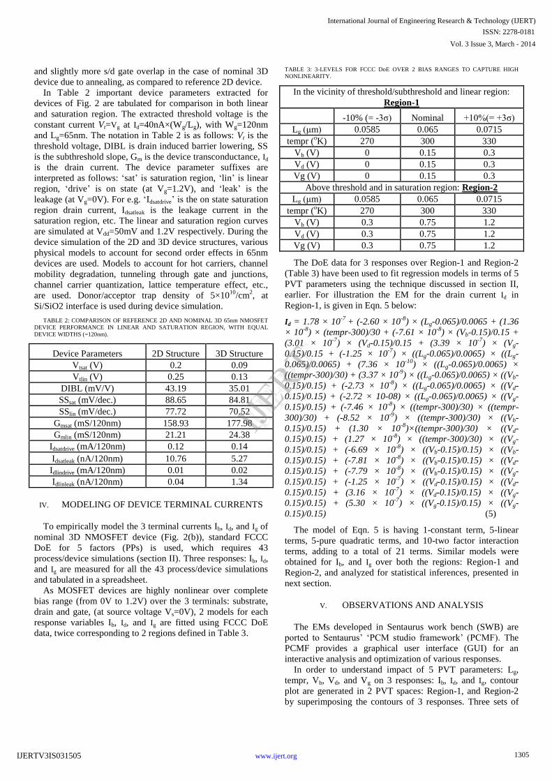
interactively in PCMFs’ GUI as shown in Fig. 5. Three
isolines form a set of contours corresponding to a given
response. These 3 isolines demarcate light colored, white
colored and dark colored regions (Fig. 5). The light color
represents the values of response less than selection range.
The dark color represents the values of response higher than
the selection range, and white color represents the value of the
response, within the selection range. Different colors are used
to distinguish different responses.
The PPs’ influence on the 3 responses: Ib, Id, and Ig in
Region-1 and Region-2 of the PVT space is mapped on an X-
Y plane as shown in Fig. 5. In this figure quantities plotted on
X and Y axes are the tempr and Vd, respectively. The white
region in the tempr-Vd plane is the intersection area of
selection ranges for the 3 responses. There are two ranges,
first: each variable in an EM will have an allowable ±3σ (i.e.,
±10%) range and second: a ‘selection range (SR). The SR
must lie within ±3σ range for any PVT PP. The SR of a
response depends on whether it has any specified target value,
for e.g. Vt of the device. Responses may also need to be
maximized, for e.g. drain current; some responses may need to
be minimized, for e.g. leakage.
The common (white) SR contains simultaneously optimized
(contour or isoline) values for the 3 responses in the tempr-Vd
plane. In Fig. 5, the choice of values of remaining 3
parameters (Lg, Vb, and Vg) has to be done carefully such that
common SR (CSR) corresponding to simultaneously
optimized responses remains within tempr-Vd plane. The
ranges of the setting for these 3 parameters such that the CSR
lies within tempr-Vd plane constitute the process window [13].
Fig. 5(a) and (b) are the contour plots (response surfaces)
corresponding to the EMs of 3 responses: Ib, Id, and Ig in
Region-1; and Fig. 5(c) and (d) are the contour plots
corresponding to the EMs of same 3 responses in Region-2. In
Fig. 5(a) setting Vb to zero causes partly visible CSR in tempr-
Vd plane. Among 3 isolines in the CSR the red is the expected
Id, green is the expected Ib, and the blue is the expected Ig.
In Fig. 5(b) setting Vb to 0.15V results in larger CSR visible
in tempr-Vd plane, with the locations of red, green and blue
contours being changed. The new location of red, green and
blue isolines may be desired or not have to be decided from
the process stability perspective.
Fig. 5(c) and (d) are the contour plots corresponding to the
EMs of 3 responses: Ib, Id, and Ig in Region-2. In Fig. 5(c)
setting Vb to 0.3V causes a small CSR visible in tempr-Vd
plane. Again, among the 3 isolines visible, the red is the
expected Id, green is the expected Ib, and the blue is the
expected Ig. In Fig. 5(d) setting Vb to 0.6V results in larger
CSR visible in tempr-Vd plane, with the location of the red,
green and blue contours being changed. The new location of
red, green and blue isolines is the desired one or not, has to be
decided from the process stability perspective.
CSR CSR
(a) (b)
SSR SSR
CSR
CSR
(c) (d)
Fig. 5: The contour plot representation of response surfaces for Ib, Id, and Ig
in tempr and Vd space for the 2 sets of EMs (a) and (b) in Region-1, and (c)
and (d) in Region-2.
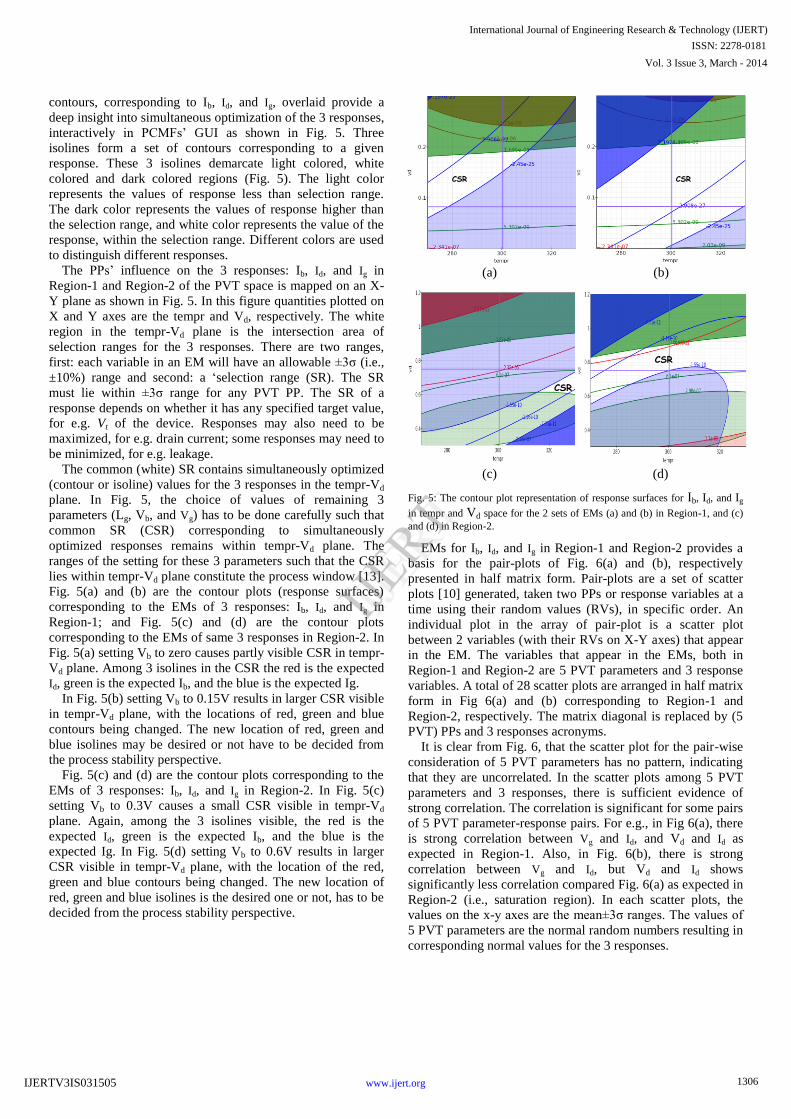
EMs for Ib, Id, and Ig in Region-1 and Region-2 provides a
basis for the pair-plots of Fig. 6(a) and (b), respectively
presented in half matrix form. Pair-plots are a set of scatter
plots [10] generated, taken two PPs or response variables at a
time using their random values (RVs), in specific order. An
individual plot in the array of pair-plot is a scatter plot
between 2 variables (with their RVs on X-Y axes) that appear
in the EM. The variables that appear in the EMs, both in
Region-1 and Region-2 are 5 PVT parameters and 3 response
variables. A total of 28 scatter plots are arranged in half matrix
form in Fig 6(a) and (b) corresponding to Region-1 and
Region-2, respectively. The matrix diagonal is replaced by (5
PVT) PPs and 3 responses acronyms.
It is clear from Fig. 6, that the scatter plot for the pair-wise
consideration of 5 PVT parameters has no pattern, indicating
that they are uncorrelated. In the scatter plots among 5 PVT
parameters and 3 responses, there is sufficient evidence of
strong correlation. The correlation is significant for some pairs
of 5 PVT parameter-response pairs. For e.g., in Fig 6(a), there
is strong correlation between Vg and Id, and Vd and Id as
expected in Region-1. Also, in Fig. 6(b), there is strong
correlation between Vg and Id, but Vd and Id shows
significantly less correlation compared Fig. 6(a) as expected in
Region-2 (i.e., saturation region). In each scatter plots, the
values on the x-y axes are the mean±3σ ranges. The values of
5 PVT parameters are the normal random numbers resulting in
corresponding normal values for the 3 responses.
1306
Vol. 3 Issue 3, March - 2014
International Journal of Engineering Research & Technology (IJERT)
IJERT
IJERT
ISSN: 2278-0181
www.ijert.orgIJERTV3IS031505
(a)
(b)
Fig. 6: Pair plots from EMs of 5 PVT parameters and 3 terminal currents of NMOSFET depicted as half -matrix. (a) in Region-1 (500 random
experiments) and (b) in Region-2 (1000 random experiments).
Looking at responses, there is a strong correlation between
Id and Ib both in Region-1 and Region-2. Even though there is
some haze (due to numerical noise, model insufficiency, etc.)
some plots in last 3 rows of Fig. 6(a) and (b), one can see
considerable dependence/correlation on PVT parameters and
among the responses themselves.
The percentage contribution of 5 PVT parameters to Ib, Id,
and Ig, derived from the Pareto chart for 3 responses is
presented in Table 4 in both Region-1 and Region-2. The
overall contribution of Vg on the 3 response variables is
highest, both in Region-1 and region-2. The contribution of
drain bias Vd to Id and Ig is almost same as Vg in Region-1; the
significant contribution of Vd to Id continues in Region-2,
which is the manifestation of DIBL and channel length
modulation (CLM) effect. Among non-electrical parameters,
the response Ig has stronger dependence on Lg and tempr. As
the gate current is due to hot carrier injection and various
tunneling effects, Ig is likely to increase with temperature.
Also, Ig being the total gate current, it is total gate area
dependant, which in turn makes it Lg dependent.
The simulation study of this research highlights significant
gate and substrate currents due to severe SCE, which is
effectively captured by 3D process/device simulations.
Further, this fact is corroborated by models of Ib, Id, and Ig.
The process/device simulation, modeling of Ib, Id, and Ig, and
statistical analysis of the models is done using Synopsys’
Sentaurus TCAD and PCM studio.
The method of process/device simulation, modeling and
statistical analysis of this paper is very useful in the present
context of IC manufacturing. Any Information based on
manufacturing process modeling of performance parameters
of interest is a valuable input to process control to minimize
process variability, which in turn achieves good performance
of ICs and result in high yield.
TABLE 4: THE PERCENTAGE CONTRIBUTION OF 5 PVT PARAMETERS OBTAINED
FROM PARETO CHART FOR THE 3 RESPONSES.
Parameters Ib Id Ig
Region-1
Lg 3.43% 2.54% 14.43%
tempr 1.97% 2.80% 16.41%
Vb 10.05% 4.30% 23.15%
Vd 39.76% 44.34% 23.08%
Vg 44.78% 46.03% 22.94%
Region-2
Lg 5.01% 4.90% 5.53%
tempr 6.16% 4.62% 6.91%
Vb 2.47% 7.72% 30.02%
Vd 43.21% 19.04% 26.78%
Vg 43.15% 63.72% 30.76%
VI. CONCLUSIONS
In view of accurate modeling of the 3 terminal currents of
NMOS transistor of a 65nm SRAM cell in terms of process,
voltage and temperature (PVT) parameters 3D device structure
is process/device simulated and optimized using dose
matching technique. The dose matching technique involves
mapping optimized 2D devices’ analytical implant profiles to
3D devices’ implant doses. The dose matching technique has
saved computation time and resources by than an order.
Standard 3-level FCCC DoE based second order EMs for the 3
responses Ib, Id, and Ig in terms of 5 PVT parameters Lg, tempr,
Vb, Vd, and Vg, is obtained using standard techniques. The 3-
levels for 5 PVT parameters are nominal value, and ±10%
(±3σ) of nominal values. Detailed statistical analysis of the
EMs has been done through contour plots, pair-plots, and
Pareto charts. Correlations among 5 PVT parameters and 3
response currents are predicted to underscore second order
effects in 65nm regime SRAM technology. The phenomenon
of process drift is analyzed using contour plots of EMs for Ib,
1307
Vol. 3 Issue 3, March - 2014
International Journal of Engineering Research & Technology (IJERT)
IJERT
IJERT
ISSN: 2278-0181
www.ijert.orgIJERTV3IS031505

Id, and Ig. A quantitative assessment of relative impact of 5
PVT parameters on Ib, Id, and Ig are performed. The method of
process/device simulation, modeling and statistical analysis of
this paper is very useful in the present context of IC
manufacturing. Any Information based on manufacturing
process modeling of performance parameters of interest is a
valuable input to process control to minimize process
variability, which in turn achieves good performance of ICs
and lead to high process yield.
ACKNOWLEDGMENT
Author would like to acknowledge Visvesvaraya
Technological University (VTU), Belgaum, Karnataka, for
funding this research project. Authors also convey special
thanks to the Management of Dayananda Sagar Group of
Institutions (DSI) for all its support and constant
encouragement for this research work.
REFERENCES
[1] Zhiqiang Ge and Zhihuan Song, “Semiconductor Manufacturing
Process Monitoring Based on Adaptive Substatistical PCA” IEEE Transaction on Semiconductor Manufacturing,, Vol. 23, No. 1, pp. 99-
108, Feb. 2010
[2] Wei-Ming Wu, Fan-Tien Cheng, and Fan-Wei Kong “Dynamic-Moving-Window Scheme for Virtual-Metrology Model Refreshing”, IEEE
Transactions on Semiconductor Manufacturing, Vol. 25, No. 2, pp. 238-
246, May 2012 [3] Dekong Zeng, and Costas J. Spanos, “Virtual Metrology Modeling for
Plasma Etch Operations”, IEEE Transactions on Semiconductor
Manufacturing, Vol. 22, No. 4, pp. 419-431, Nov. 2009. [4] Chihyun Jung and Tae-Eog Lee, “An Efficient Mixed Integer
Programming Model Based on Timed Petri Nets for Diverse Complex
Cluster Tool Scheduling Problems”, IEEE Transactions on
Semiconductor Manufacturing, Vol. 25, No. 2, pp. 186-199, May 2012. [5] YT. Tai, WL. Pearn, and Chun-Min Kao, “Measuring the
Manufacturing Yield for Processes With Multiple Manufacturing Lines”,
IEEE Transaction on Semiconductor Manufacturing, Vol. 25, No. 2, pp. 284-290, May 2012.
[6] Gareth Roy, et al, “Comparative Simulation Study of the Different
Sources of Statistical Variability in Contemporary Floating-Gate Nonvolatile Memory”, IEEE Transactions on Electron Devices, Vol. 58,
No. 12, pp. 4155-4163, Dec. 2011.
[7] Shunichi Watabe, et al “A Simple Test Structure for Evaluating the Variability in Key Characteristics of a Large Number of MOSFETs”, IEEE Transactions on Semiconductor Manufacturing, Vol. 25, No. 2, pp. 145-154, May 2012.
[8] HC. Srinivasaiah, “Implications of Halo Implant Shadowing and
Backscattering from Mask Layer Edges on Device Leakage Current in 65nm SRAM”, in Proc. of 25th IEEE International Conference on VLSI
Design, Hyderabad, India, pp. 412-417, Jan. 2012.
[9] Y. Taur, and TH. Ning, “Fundamentals of Modern VLSI Devices”,
First edition, Cambridge University Press, 1998.
[10] HC. Srinivasaiah, “Statistical Modeling of Transistor Mismatch Effects
in 100nm CMOS devices”, Ph.D Thesis, Indian Institute of Science, Bangalore, India, July 2004.
[11] Duane S. Boning, and P. K. Mozumder, ”DOE/Opt: A System for
Design of Experiments, Response Surface Modeling, and Optimization Using Process and Device Simulation”, IEEE Transactions on
Semiconductor Manufacturing, Vol. 7, NO. 2, pp.233-244, May. 1994.
[12] R.L. Plackett and J. P. Burman, ”The Design of Optimum Multifactorial Experiments”, Biometrika, Vol. 33, Issue 4, pp. 305-325, Jun. 1946
[13] Sprocess/sdevice - TCAD Release-10 Manual, 2010.
[14] International Technology Roadmap for Semiconductor (ITRS), 2007 edition, available at: http://www.itrs.net
[15] R. Srinivasan, and Navakanta Bhat, “Effect of gate- drain/source
overlap on the noise in 90nm N-channel metal oxide semiconductor field effect transistors”, Journal of Applied physics Vol. 99, No. 8, 2006
1308
Vol. 3 Issue 3, March - 2014
International Journal of Engineering Research & Technology (IJERT)
IJERT
IJERT
ISSN: 2278-0181
www.ijert.orgIJERTV3IS031505