Embed Size (px)
Citation preview

EMCA REPORT
22/01/2013 [Radio Frequency circuit ]
Students : Abdelhakim ZOUAKI
Cong VU HUY
Teachers : Etienne SICARD
Sonia BEN DHIA
EMCA Report
Page 1
EMCA Report
INTRODUCTION
In this report we will try to study some radio frequency circuits and describe the general context of this kind
of circuits.
We studied in this paper many types of circuits that are based on CMOS transistors and always used for
wireless connection, these circuits are: Power amplifier Class A and Class B, Oscillators, Phase-Lock Loop
and Voltage-Controlled Oscillator.
Nowadays, researchers are trying to optimize ICs performances by trying to raise up speed, lowering power
consumption and dealing at the same time with linearity, temperature and noise problems.
Here are some examples of technologies that use the RFIC: WLAN, UWB, mobile and cordless phones,
RFIDs, Zigbee and Bluetooth devices. This shows that Radio Frequency has become more and more
interesting in wireless communication.
EMCA Report
Page 2
Contents
I. Resonance ............................................................................................... 3
II. Oscillators ............................................................................................. 6
1. NMOS: ................................................................................................ 6
2. PMOS: ................................................................................................. 7
3. Gate NOT: ........................................................................................... 8
4. Oscillator: ............................................................................................ 9
III. Power amplifier ................................................................................... 10
1. Power amplifier efficiency (PE): ...................................................... 10
2. Class of power amplifier: .................................................................. 11
IV. Voltage-Controlled Oscillator ............................................................. 12
V. Conclusion .......................................................................................... 13

EMCA Report
Page 3
I. Resonance
In this part we tried to simulate the output of an integrated inductor and we saw that a perfect inductor
doesn’t exist, that means, in all circuits we have to deal with parasite parameters as resistances and
capacitances.
Figure 1: Resonance of a coil
As it can be seen a spool can be represented by a serial combination of a resistor and inductor connected with
two parallel capacitors as showed in figure 2.
In fact, the spool is equivalent to a resonant RLC circuit which has the following resonance frequency:
To check the result we calculated the numerical value of the resonance’s frequency. fresonance = 0.9266GHz.
It’s the same as in the resonance crest in the red graph, figure1.
Figure 2: Equivalent model of a coil
We have to be very careful while speaking about the resonance frequency of the coil because the two
parasitic capacitors are different, therefore the frequency will depend on the plug in of the input signal (either
point A or B of the figure 1).
A
B
EMCA Report
Page 4
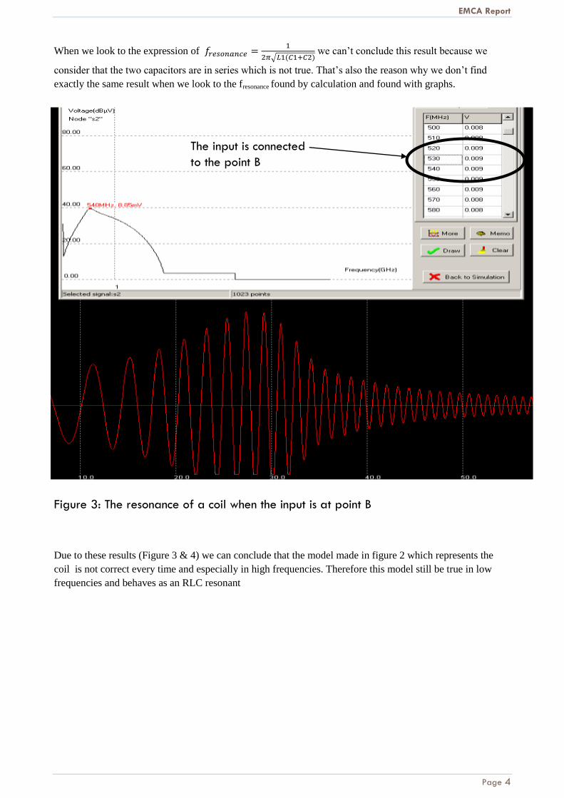
When we look to the expression of
we can’t conclude this result because we
consider that the two capacitors are in series which is not true. That’s also the reason why we don’t find
exactly the same result when we look to the fresonance found by calculation and found with graphs.
Figure 3: The resonance of a coil when the input is at point B
Due to these results (Figure 3 & 4) we can conclude that the model made in figure 2 which represents the
coil is not correct every time and especially in high frequencies. Therefore this model still be true in low
frequencies and behaves as an RLC resonant
The input is connected
to the point B
EMCA Report
Page 5
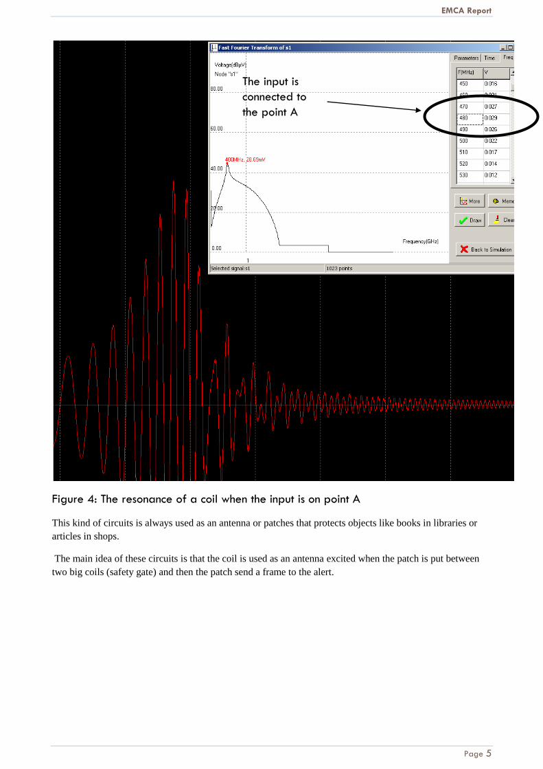
Figure 4: The resonance of a coil when the input is on point A
This kind of circuits is always used as an antenna or patches that protects objects like books in libraries or
articles in shops.
The main idea of these circuits is that the coil is used as an antenna excited when the patch is put between
two big coils (safety gate) and then the patch send a frame to the alert.
The input is
connected to
the point A
EMCA Report
Page 6
II. Oscillators
The oscillators that we present here is a system using the NMOS and CMOS structures assembled
together in order to generate a sinus signal itself.
First of all, we will make a quick review of the NMOS and CMOS structures and how it works.
1. NMOS:
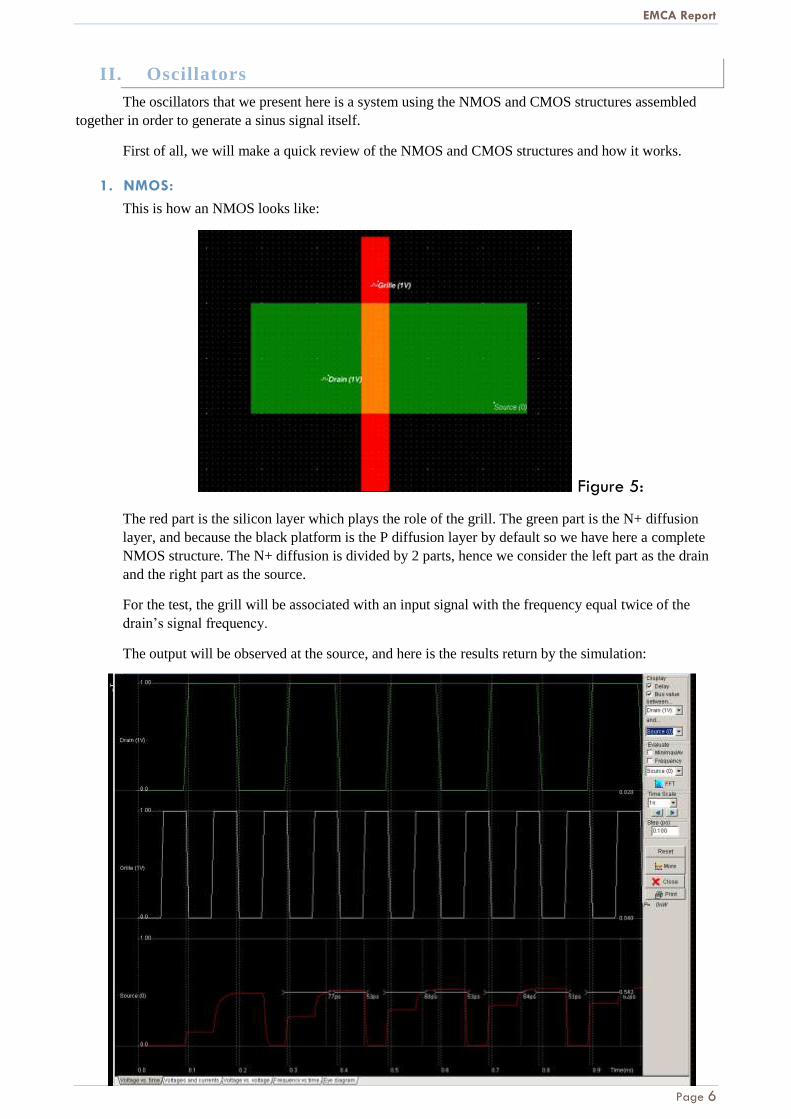
This is how an NMOS looks like:
Figure 5:
The red part is the silicon layer which plays the role of the grill. The green part is the N+ diffusion
layer, and because the black platform is the P diffusion layer by default so we have here a complete
NMOS structure. The N+ diffusion is divided by 2 parts, hence we consider the left part as the drain
and the right part as the source.
For the test, the grill will be associated with an input signal with the frequency equal twice of the
drain’s signal frequency.
The output will be observed at the source, and here is the results return by the simulation:
EMCA Report
Page 7
The principle work of this structure is:
When Vgrill = 0V, the source stays constant.
When Vgrill = 1V (or different of 0 for all the other cases), the source recopies the value of
the drain.
However, we can see clearly that the signal of the source is not quite coherent. All this is caused
by the different frequency of the grille and the drain. When Vgrill = 1V at the first time, Vdrain = 0
always. When Vgrill returns to 0V, the source begins to recopy the drain slowly, but he isn’t able to
reach the maximum. In the next period of Vgrill = 1V, the source can finally reach the maximum,
but it is still not 1V, but 1V – Vt (Vt is the voltage parasite, or the threshold voltage) .
We can see that a NMOS structure drives well a “0” logic but poorly a “1” logic.
2. PMOS:
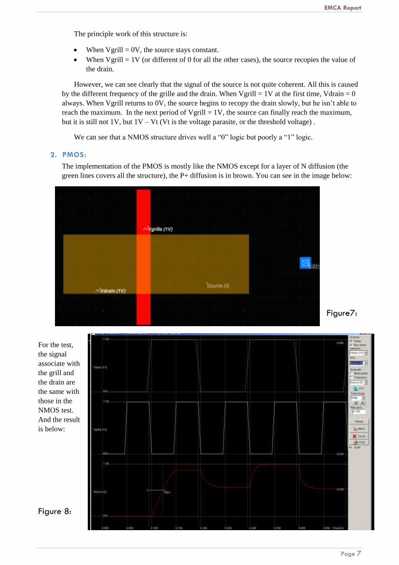
The implementation of the PMOS is mostly like the NMOS except for a layer of N diffusion (the
green lines covers all the structure), the P+ diffusion is in brown. You can see in the image below:
Figure7:
For the test,
the signal
associate with
the grill and
the drain are
the same with
those in the
NMOS test.
And the result
is below:
Figure 8:

EMCA Report
Page 8
This structure works with the following principle:
When Vgrill = 1V (or different of 0 for all the other cases), the source stays constant.
When Vgrill = 0, the source recopies the value of the drain.
At first, Vsource = 0, then when Vgrill = 0 and Vdrain = 1V, the source recopies the value 1slowly.
With this structure, we can see that the source recopies well the value 1 of the drain but the value 0 is
incremented by Vt (V parasite, or threshold) .
We can jump to the conclusion that a PMOS structure drives well a “1” logic but poorly a “0” logic.
3. Gate NOT:
A structure of a NMOS and a PMOS that take advantage of their properties (drives well a
“0” or “1” logic) to create a simple function but with no default.
The implementation of this structure is as the image below:
Figure 9:
The 2 structures have the same grill in order to make sure only 1 of these 2 drives: the
PMOS drives when Ve is at “0” logic, and the NMOS drives when Ve is at “1” logic. When the
PMOS drives, the source recopies the value Vdd (“1” logic) of the drain. So with Ve = “0”, Vs =
“1”. We have also a same assertion with the NMOS, or Ve = “1”, Vs = “0”. So we created a NOT
gate.
Ve (Grill)
PMOS
NMOS
V = 0
V = Vdd
Vs
EMCA Report
Page 9
4. Oscillator:
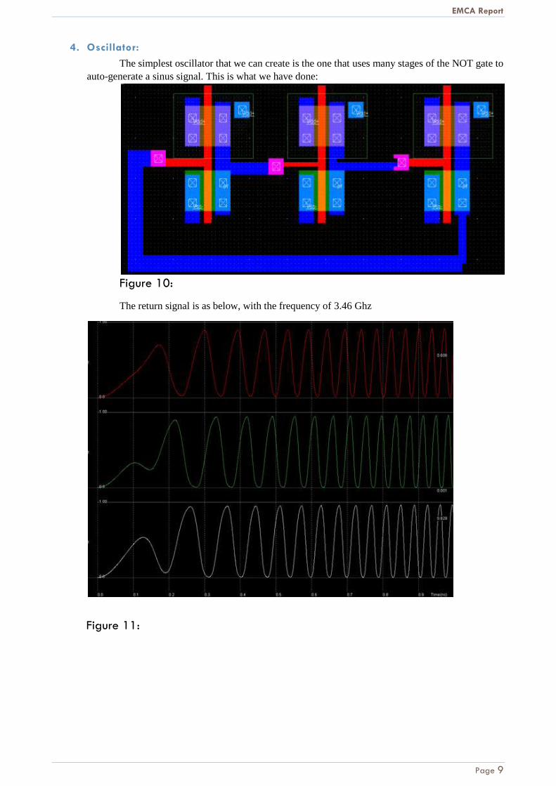
The simplest oscillator that we can create is the one that uses many stages of the NOT gate to
auto-generate a sinus signal. This is what we have done:
Figure 10:
The return signal is as below, with the frequency of 3.46 Ghz
Figure 11:
EMCA Report
Page 10
III. Power amplifier
1. Power amplifier efficiency (PE):
The evolution of power amplifier is based on this characteristic. It is calculated by the power delivered
by the circuit (and send to the resistance load) divided by the power of the supply source.
PE = Pout
Psupply
PE is usually calculated in %
The power with a low ¨PE have a low consumption and required a low supply, so they are very
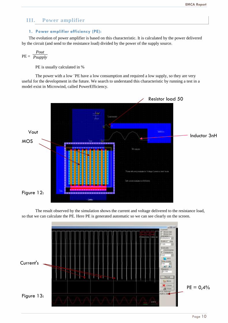
useful for the development in the future. We search to understand this characteristic by running a test in a
model exist in Microwind, called PowerEfficiency.
Figure 12:
The result observed by the simulation shows the current and voltage delivered to the resistance load,
so that we can calculate the PE. Here PE is generated automatic so we can see clearly on the screen.
Figure 13:
Inductor 3nH
Resistor load 50
ohm
MOS
device
PE = 0,4%
Current's
pic
Vout

EMCA Report
Page 11
The current's pic of the load resistor shows that this circuit consumes very low of the power supply,
it's nearly a pulse of the signal. The PE is then very small (here 0,4%).. Hence, this value will be a critical to
determine the performance of a power amplifier.
The technology of power amplifier consists of a product with this lowest characteristic if possible.
And after the output signal, we will place a detection of amplitude to reconstruct the signal. This is a good
way to economize energy and still have a good conception.
2. Class of power amplifier:
The difference between the classes is the form of the signal output. Class A has a signal sinusoidal
while class B has a signal sinusoidal demi-period. As represented above, we can see that class B has a lower
consumption than class A.
The image below is the response of current I with class A and class B. We can observe easily the PE
of class B is lower than class A when we applied a resistor load 50 ohm.
Figure 14: Class A signal output
Figure 15: Class B signal output
PE = 15.7%
PE = 22.3%
EMCA Report
Page 12
IV. Voltage-Controlled Oscillator
In this part we will study a circuit mostly used in modulation, this circuit is the VCO. One of the causes that
motivated us to work on it is that we worked on this circuit to modulate and demodulate a signal using an
Amplitude Modulation and Frequency Modulation without looking after its intern operating and now is the
opportunity for us to do it.
A VCO is a circuit that when we apply a voltage in its input it gives us a corresponding signal with a
specified frequency. It’s used to generate a signal with a certain frequency dependent on the input voltage In.
The figure 16 which is an FFT of the simulation of existing schematics on examples of the software we can
easily see the relation between the frequency of the output signal of the VCO and its input voltage.
Figure 16
The important point that we can notice is that when we apply a zero voltage at the input of the VCO this one
give us an output signal with a very high frequency.
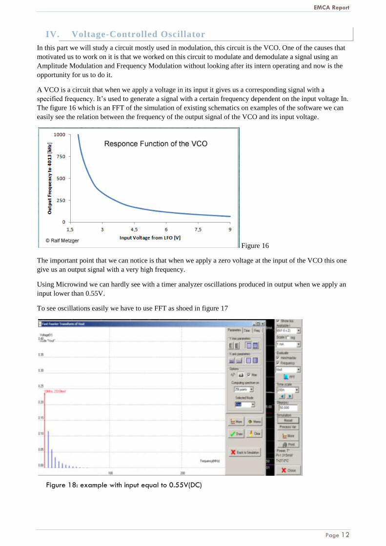
Using Microwind we can hardly see with a timer analyzer oscillations produced in output when we apply an
input lower than 0.55V.
To see oscillations easily we have to use FFT as shoed in figure 17
Figure 18: example with input equal to 0.55V(DC)

EMCA Report
Page 13
V. Conclusion
This project allowed us to go deeply into the operating principle of some usual circuits and see how they are
used in RFID and we also discovered the general context of this kind of circuits.
It was very interesting for us to discover how to design CMOS cells like transistor, inductance or capacitor,
Power amplifiers, Oscillators and many other circuits.
We also observed in this report many problems that nowadays researchers are trying to optimize like power
consumption (in the power amplifier) or noise.


![Tutorial_Manual Microwind 1.d[1]](https://img.dokumen.tips/doc/110x75/5540d36d4a7959f00c8b4b0f/tutorialmanual-microwind-1d1.jpg)