Embed Size (px)
Citation preview

SUPPLEMENTARY INFORMATION
Nanowires as semi-rigid substrates for growth of thick, InxGa1-xN (x>0.4) epi-layers
without phase segregation for photoelectrochemical water splitting.
Chandrashekhar Pendyala1, Jacek B. Jasinski
2, Jeong H. Kim
1, Venkat Kalyan Vendra
1, Sergey
Lisenkov,3 Madhu Menon
4 and Mahendra K. Sunkara
1,2,*
1 Department of Chemical Engineering, University of Louisville, Louisville KY 40292
2 Conn Center for Renewable Energy Research, University of Louisville, Louisville, KY 40292
3 Department of Physics, University of South Florida, Tampa, FL 33620-5700
4 Department of Physics and Astronomy and Center for Computational Sciences, University of Kentucky, Lexington,
KY 40506 * Email: [email protected]
Electronic Supplementary Material (ESI) for NanoscaleThis journal is © The Royal Society of Chemistry 2012

EXPERIMENTAL SET UP FOR THE SYNTHESIS OF GaN NANOWIRES
Figure S1a is the schematic of the reactor used for the synthesis of GaN nanowires via thermal
CVD. The reaction vessel is a double walled, water cooled stainless steel chamber. Pressure
measurement is via an MKS-Baratron dual capacitance manometer and temperature is measured
using a noncontact dual wavelength pyrometer. A stem runs through the bottom of the chamber
via a vacuum sealed connection for the heater assembly. A serpentine tungsten filament serves as
the heat source that radiatively heats a SiC (silicon carbide) coated graphite plate placed 1 cm
above. The source materials (GaN powder or gallium metal) are placed on the graphite plate
while the substrate (stainless steel plate) is placed 2-3 mm above the sources via graphite
supports. Figure s1b is the schematic of the MOCVD reactor used for InGaN growth. The reactor
has a multi precursor delivery system along with an induction heater for substrate heating. The
reaction chamber is a vertical flow type with a showerhead at the top for uniform precursor
distribution.
Figure S1: a) Schematic of the CVD reactor used for the synthesis of GaN nanowires. GaN
powder or Ga metal was placed on the graphite susceptor and the substrate was placed 2-3 mm
off the surface using graphite blocks as separators. b) Schematic of the MOCVD reactor showing
the multi precursor delivery system along with the vertical flow reaction chamber with a
showerhead for uniform precursor distribution and an induction heater for substrate heating.
Electronic Supplementary Material (ESI) for NanoscaleThis journal is © The Royal Society of Chemistry 2012

ORENTIATION CONTROLLED SYNTHESIS OF GaN NANOWIRES
GaN nanowires were synthesized on different substrates under variations of flux and temperature
conditions to investigate the influence of substrate on the growth mechanism to control the
growth morphology as well as orientation. Substrates ranging from metals (copper and stainless
steel), semiconductors (<100> silicon and c-GaN on sapphire) to insulators (sapphire) were
employed in the study. Two different process conditions were devised to achieve different
gallium flux conditions. In one case, gallium metal was heated to 750C to generate the gallium
vapors in a low pressure (300 mTorr) ammonia atmosphere. In the other condition, pre
synthesized GaN powder was used as the gallium source. The powder was heated to 950C in 20
Torr ammonia atmosphere.
Figure S2 shows the template to achieve the desired nanowire growth on different
substrates. It is clear that substrate as well as process conditions have a big impact on the
nanowire growth.
Figure S2: Template for process and substrate selection for controlled growth of GaN nanowires.
Metal substrates can always be used to grow nanowires using the developed process window
whereas nanowire growth on semiconductor or insulators is heavily affected by the wetting
behavior of gallium.
The wetting behavior of gallium on the substrate surface controls the nuclei formation,
hence the nanowire growth. Under the low temperature and high flux conditions (at 750 C using
gallium metal), gallium spreads like a film on the non-metallic substrates before crystal nuclei
formation can take place. However, the metals could be catalyzing the GaN formation reaction as
GaN nuclei form on the metal surfaces and lead the nanowire growth. The non-metallic
Electronic Supplementary Material (ESI) for NanoscaleThis journal is © The Royal Society of Chemistry 2012

substrates might are not at high enough temperatures to cause the reaction of gallium with
nitrogen.
At the high temperature conditions, the surface temperature on all the substrates is high
enough for the gallium flux to react and form GaN nuclei leading to nanowire growth. Here, the
stability of the nuclei at the high temperatures and the interactions of the substrate control the
growth orientation. C-GaN is the most stable surface at high temperatures and hence the
formation of c-plane oriented nanowires on all metal and semiconductor surfaces. However, a-
plane GaN nanowires grow on quartz substrates. Quartz is not a good thermal conductor and the
surface might be at a lower temperature than other substrates that are good thermal conductors.
At lower temperatures a-plane nuclei has lower energy of formation. This is indeed the case
observed for the growth on stainless steel substrates. At higher temperatures, c-GaN nanowires
are formed whereas at low temperatures, a-plane oriented GaN nanowires grow on the substrate.
COMPOSITION CONTROL OF InGaN LAYERS ON GaN NANOWIRES
As described in the article text, MOCVD was used to synthesize InGaN layers on GaN
nanowires. TMGa and TMIn were used as the gallium and indium sources with NH3 as the
nitrogen source. Figure S3 is our reactor specific template/ process window for the temperature
and flux based control of InGaN composition. Although it is definitely not exhaustive, this
provides a good starting point to further tune the reactor and process conditions for the synthesis
of InGaN layers on GaN nanowires.
R is the ratio of the TMIn and TMGa flux with TMGa flux maintained at 10 µmol/min.
TMIn flux is varied to change R. GaN is generally synthesized at 800 C- 900 C and InN at 550 C
- 600 C. Hence, 700 C - 750 C range was of interest to attain 50-50 In-Ga content. Figure S3 is
the plot of the indium content in the InGaN alloys at different combinations of temperatures and
flux ratios.
Electronic Supplementary Material (ESI) for NanoscaleThis journal is © The Royal Society of Chemistry 2012

Figure S3: Plot of the indium content in InGaN alloys obtained with different sets of process
parameters. R is the ratio of the TMIn/TMGa flow rates. At constant flux, indium content
decreases with increase in temperature, due to the increased indium desorption at high
temperatures. At constant temperatures, as R (indium/gallium flux ratio) is increased, indium
content also increases.
MORPHOLOGY OF InGaN GROWTH ON GaN NANOWIRES
As described in the article text, orientation dependent growth of InGaN was observed on GaN
nanowires. Formation of complete hexagonal shells of different thicknesses is clearly shown in
figure S4.
On c-GaN nanowires
Figure S4: SEM images of the InGaN shell formation on various samples. The formation of a
uniform hexagonal shell with the GaN wire protruding at the center.
Electronic Supplementary Material (ESI) for NanoscaleThis journal is © The Royal Society of Chemistry 2012

On a-GaN nanowires
As shown already in figure 2 in the main article, growth is very different on a-GaN nanowires.
The pyramids grow radially out from the two polar (0001) and (000-1) surfaces which is clearrly
shown in figure S5a. The hexagonal shape of the pyramids is clear from the top view in figure
S5b. The island coalescence into a shell bound by four facets is clear in figure S5c which also
shows the hexagonal island at the tip. Finally, another perpective of the InGaN shell completely
covering the GaN nanowire is shown in figure S5d.
Figure S5: Perspective of the heteroepitaxial growth of InGaN on a-GaN nanowires. a) The
pyramidal islands grow on the surface and not along the surface (for c-GaN nanowires) of the
nanowire. The islands grow only on the two polar (0001) and (000-1) surfaces. b) Top view of
the pyramids clearly shows the hexagonal shape of the islands. c) Side view of the growth of
islands after coalescence clearly showing the coalesced pyramids forming a four faceted shell.
d) InGaN shell on the nanowire.
Electronic Supplementary Material (ESI) for NanoscaleThis journal is © The Royal Society of Chemistry 2012

DISTRIBUTION OF THE SPECIES IN InGaN LAYERS
Distribution of the species (gallium and indium) in the InGaN layers needs to be ascertained to
determine the uniformity of the composition and show the lack of any phase segregation.
Figure S6 is the elemental map of InGaN growth on a-GaN nanowires showing the
islands growing on the nanowires. GaN nanowire is clearly visible in the gallium map as the
bright line and is conspicuously absent from the indium map. The maps clearly show the uniform
distribution of the species in the alloy islands indicating the absence of phase separation.
Figure S6: TEM EDS elemental map of InGaN growth on GaN nanowire. An image of the
growth is also included for reference. The gallium and indium maps show uniform composition
distribution without any phase segregation. Also, the GaN nanowire clearly shows up in the
gallium map which should be and is absent from the indium map.
Figure S7 is the STEM EDS elemental map of InGaN growth on c-GaN nanowires.
The partially coalesced islands can be seen aligned along the length of the nanowire. Similar to
figure S6, the nanowire shows up in the gallium map. The material distribution is uniform in this
case as well in the InGaN layers indicating the absence of any phase segregation.
Electronic Supplementary Material (ESI) for NanoscaleThis journal is © The Royal Society of Chemistry 2012

Figure S7: TEM EDS elemental map of InGaN growth on GaN nanowire. An image of the
growth is also included for reference. The gallium and indium maps show uniform composition
distribution without any phase segregation. Also, the GaN nanowire clearly shows up in the
gallium map which should be and is absent from the indium map.
Electronic Supplementary Material (ESI) for NanoscaleThis journal is © The Royal Society of Chemistry 2012

STUDY OF InGaN ISLAND NUCLEATION
According to the proposed growth mechanism, step nucleation and growth leads to the formation
of islands at the very initial stage, followed by the growth of islands while maintaining a constant
growth rate. Aspect ratio of islands of different sizes was measured for growth on a-GaN as well
as c-GaN nanowires. This is indeed the observation as extremely small as well as large islands
with the same aspect ratio have been observed as shown in figure S8.
Figure S8: SEM micrograph of the InGaN growth on GaN nanowires. Islands with different sizes
are shown indicating that the islands form at the very initial stages followed by the island growth
at constant aspect ratio.
Wurtzite crystals have a characteristic c/a ratio of 1.63. However, looking from the top,
the perspective correction has to be applied. As shown in the schematic S9, the height of the
pyramid is the “c” and depending on the orientation of the base, it is either 1.73a or 2a. Hence,
using the wurtzite c/a ratio, the measured height/base ratio in the two cases should be 0.94
(1.63/1.73) and 0.815 (1.63/2) respectively.
Figure S10 is the compilation of the height and base of the pyramids of different sizes
measured on samples with different InGaN concentrations. The data in red is for the pyramids
where two facets were visible which resulted in a 0.92 ratio and the data in black is for the
pyramids where three facets were visible resulting in a ratio of 0.81 that agrees closely with the
expected values.
Electronic Supplementary Material (ESI) for NanoscaleThis journal is © The Royal Society of Chemistry 2012

Figure S9: Schematic of the two possible views of the hexagonal pyramidal islands. The base is
equal to 1.72 times the lattice constant “a” when only two facets are visible whereas the
measured base would be twice the lattice constant “a” when three facets are visible.
Figure S10: Aspect of the pyramidal islands of different sizes and different InGaN compositions.
Number of facets of the pyramid visible in the plan view controls the ratio. The steps form a
pyramidal shape at very initial stages and grow in size maintain the aspect ratio. The size of the
pyramids has been measured from < 5 nm (smallest) to > 100 nm (largest), corroborating our
proposed growth mechanism.
The observed trend and the consistent aspect ratio of the pyramidal islands indicate that
the growth of the steps occurs at a constant velocity in the direction of the inclined (10-11) facet.
This supports the proposed growth mechanism that step flow and growth forms the pyramids
during very early stages of the growth.
Electronic Supplementary Material (ESI) for NanoscaleThis journal is © The Royal Society of Chemistry 2012

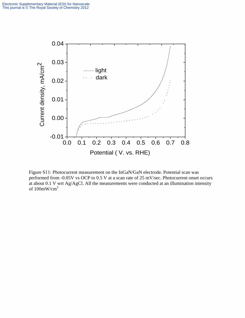
PHOTOACTIVITY OF InGaN/GaN NANOWIRE STRUCTURES:
Photocurrent measurements:
A three electrode setup was used to measure the photocurrent of the InGaN/GaN nanowire
structures. The working and counter electrodes are similar to the two electrode measurements
and a Ag/AgCl reference electrode is also introduced in the system. A voltage sweep is made
from -0.05V wrt OCP and 1 V while measuring the current.
The measurement is repeated in dark and under illumination (100 mW/cm2 AM 1.5) to
determine the photoactivity of the material as shown in figure S11. The photocurrent
measurements on two different electrodes with similar InGaN growth showing the need for
optimization of the back contact process. Photoactivity is observed in both cases but the current
is an order of magnitude smaller in the second electrode.
0.5 0.6 0.7 0.8 0.9 1.0-0.2
-0.1
0.0
0.1
0.2
0.3
Curr
ent
density,
mA
/cm
2
Potential ( V. vs. RHE)
light
dark
Electronic Supplementary Material (ESI) for NanoscaleThis journal is © The Royal Society of Chemistry 2012
0.0 0.1 0.2 0.3 0.4 0.5 0.6 0.7 0.8-0.01
0.00
0.01
0.02
0.03
0.04C
urr
ent
density,
mA
/cm
2
Potential ( V. vs. RHE)
light
dark
Figure S11: Photocurrent measurement on the InGaN/GaN electrode. Potential scan was
performed from -0.05V vs OCP to 0.5 V at a scan rate of 25 mV/sec. Photocurrent onset occurs
at about 0.1 V wrt Ag/AgCl. All the measurements were conducted at an illumination intensity
of 100mW/cm2
Electronic Supplementary Material (ESI) for NanoscaleThis journal is © The Royal Society of Chemistry 2012

Stability of the electrodes
Figure S12: Stability measurements of the InGaN/GaN electrode measured at 0.5 V and 100
mW/cm2 illumination. a) Photocurrent is measured on the second electrode which shows a fairly
stable behavior. SEM images of the InGaN coating b) before and c) after the term photocurrent
testing.
Electronic Supplementary Material (ESI) for NanoscaleThis journal is © The Royal Society of Chemistry 2012

Stacking faults in GaN nanowires
Figure S13 shows the presence of stacking faults in c-plane GaN NWs.grown at typical growth
temperatures of 750-850 ºC. Higher growth temperatures tend to result in stacking fault free GaN
nanowires even with c plane oriented growth direction. However, the a-direction nanowires
grown at the above growth temperatures of 750-850 ºC tend to be planar defect free. One issue is
that the a-drection nanowires tend to grow fast leading to thin and long nanowires that are not
ideally suitable for PEC applications. Efforts are currently underway to grow shorter a-direction
nanowires and also stacking fault free c-direction nanowires and use them for growing InGaN
layers for PEC testing.
Figure S13: HRTEM image showing stacking faults in c-plane GaN NWs
Electronic Supplementary Material (ESI) for NanoscaleThis journal is © The Royal Society of Chemistry 2012