Embed Size (px)
Citation preview

The embedded camera TAM of 2.5Bu is
based on an evolving growth model. CAGR
for the segment is projected to be greater
the 10% during this time period. Strong
growth, overlapping functionality and new
markets are helping to keep the embedded
camera strong for the foreseeable future.
The industry has acquired a thirst for depth
detection in the cameras, and the
generation of a point cloud of a scene, this
has the potential to increase volumes
shipped by nearly 2X by the latter part of
this decade
Embedded
Camera
Status AT THE EDGE OF DEPTH
April 2014 Research Report
AT THE EDGE OF DEPTH

1
Contents Executive Summary ....................................................................................................................................... 3
State of Mobile Camera Phone ................................................................................................................. 6
Disruption ................................................................................................................................................. 8
The promise of a depth map ..................................................................................................................... 9
Post capture manipulation .................................................................................................................... 9
Lenslet Approach ................................................................................................................................ 10
Array Camera Approach ...................................................................................................................... 10
Sensor/OEM Supplier Map ................................................................................................................. 13
Computational Camera Suppliers ....................................................................................................... 13
Smart TV Camera Market ........................................................................................................................ 14
Solutions.................................................................................................................................................. 14
Smart TV Camera Map ........................................................................................................................ 16
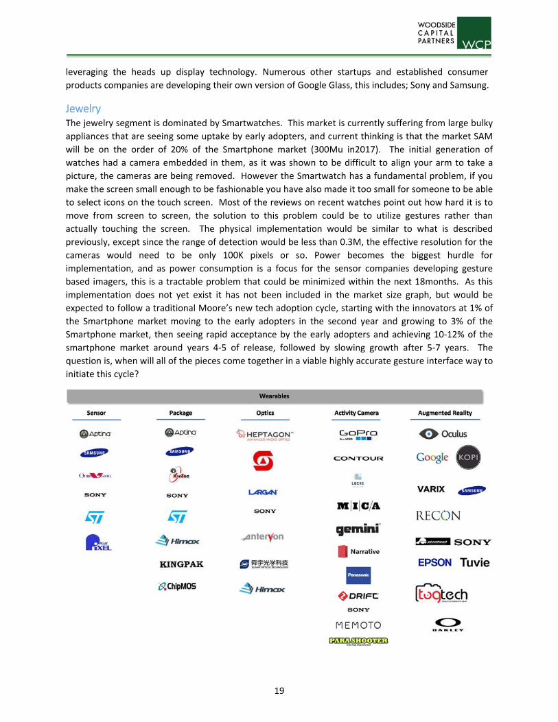
Wearables ................................................................................................................................................... 17
Activity Based Cameras ........................................................................................................................... 17
Augmented reality cameras .................................................................................................................... 18
Jewelry .................................................................................................................................................... 19
Security ................................................................................................................................................... 20
Security Camera Map .......................................................................................................................... 22
Automotive ................................................................................................................................................. 23
Channel Roles: ......................................................................................................................................... 25
Supplier Map ....................................................................................................................................... 26
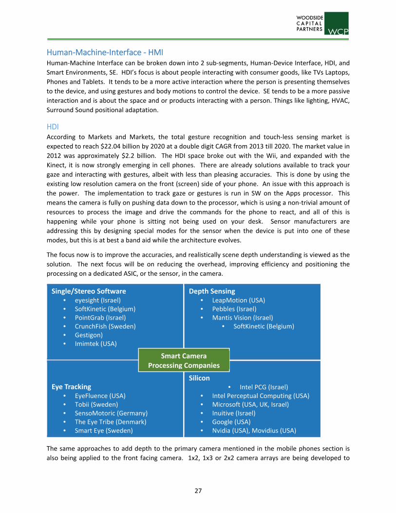
Human‐Machine‐Interface ‐ HMI ................................................................................................................ 27
HDI........................................................................................................................................................... 27
HDI Supplier Map ................................................................................................................................ 28
Smart Environments (SE) ............................................................................................................................ 29
SE Supplier Map .................................................................................................................................. 31
Technologies ............................................................................................................................................... 32
Embedded Imaging Ecosystem ............................................................................................................... 32
Traditional Sensor Evolution ................................................................................................................... 33
High Dynamic Range ........................................................................................................................... 33
Auto‐Focus (AF) Support ..................................................................................................................... 33
New Sensors ............................................................................................................................................ 34

2
Array Cameras ..................................................................................................................................... 34
Quantum Dot ...................................................................................................................................... 35
Depth .................................................................................................................................................. 36
Thermal ............................................................................................................................................... 36
Ultrasonic ............................................................................................................................................ 37
E/M‐field ............................................................................................................................................. 37
Lens ......................................................................................................................................................... 38
Speed Trends ...................................................................................................................................... 38
Auto‐Focus AF actuators ..................................................................................................................... 38
MEMs .................................................................................................................................................. 38
Liquid Crystal ....................................................................................................................................... 39
Deformable ......................................................................................................................................... 40
Modules .................................................................................................................................................. 41
OIS ....................................................................................................................................................... 41
Active Alignment ................................................................................................................................. 41
Depth ...................................................................................................................................................... 41
Structured Light .................................................................................................................................. 41
Time of Flight ...................................................................................................................................... 42
Multi‐Camera ...................................................................................................................................... 42
Image Processing .................................................................................................................................... 43
Multispectral ....................................................................................................................................... 43
Private Companies ...................................................................................................................................... 45
Components ............................................................................................................................................ 45
System/SW .............................................................................................................................................. 47
Public Companies/Divisions .................................................................................................................... 51
M&A Activity ............................................................................................................................................... 54
Appendix A: Private Company Additional Information
‐ Apical, Aptina, Chirp Microsystems, Eyesight, Eye Tech, General Vision, GeoSemiconductors,
GestureTek, InVisage, Kalray, Leap Motion, LensVector, Metaio, Movidius, Pelican, PointGrab, poLight
Appendix B: Public Company Additional Information
‐ Intel, MediaTek, Microchip, NVIDIA, Omnivision, Qualcomm, Samsung, Sony
Appendix C: Woodside Capital Partners Contact Information

3
1,150
1,430
2,138
2,729
919
1,300 1,425 1,516
0
500
1,000
1,500
2,000
2,500
3,000
2013 2014 2015 2016 2017
(M) units
Mobile Camera TAMwith Computational Camera Adoption
Smartphone (Computational Camera) Smartphone
Executive Summary Mobile Camera Market
The mobile camera market is starting to
see a significant shift from its traditional
evolution. The industry has acquired a
thirst for depth detection in the cameras,
and the generation of a point cloud of a
scene. The technologies used in
consumer products like the Kinect and
Creative Labs PC Cameras have
fundamental problems working in
sunlight. The technology that is being
adopted is based on computational
cameras. This entails utilizing multiple
lower resolution cameras to achieve a higher resolution image, and to determine the depth of objects in
the scene in a manner similar to how a pair of eyes determines depth in a scene. Pelican Imaging,
Heptagon, Lynx and CorePhotonics have first mover advantage for this approach. While also providing a
higher resolution solution and depth, because the approach is based on combining lower resolution
sensors it will also reduce the thickness of the camera module, provide better low
light performance and dynamic range. If this trend is adopted, it is expected the
volume of shipments will shift from the flattening growth currently being
experienced in the smartphone camera market to the aggressive growth shown in
the chart above. While the unit sales will see considerable growth the revenue
growth will be much less as it will be based on lower resolution imagers. Most of the current
approaches are based on utilizing existing technologies from the sensor, optics and module companies.
This means the industry will be able to shift and supply in high volumes quickly, and the differentiation
will be derived from the processing companies. This also means any companies not either ahead of the
manufacturing supply curve or addressing the potential future supply issues associated with such
aggressive growth will see its market share diminish.
The processing needed to produce the captured image is very different when compared to how the raw
data is currently processed, and is complex enough that running the processing in SW on the current
applications processors uses too much power. This presents an opportunity to general purpose
processor companies, such as GeoSemi and Movidius as additional processing will be needed.
Smart TV’s
Until the industry can get around the concern of anyone calling you through your TV and being able to
see the state of the room or how you are dressed at home they will have problems with mass adoption.
The drive to detect depth by the mobile camera market will prove to be the means to get a broader
adoption of cameras embedded into TVs. Here the focus will be on enabling gesture control of the TV
and it peripherals, as well as the opportunity to link the camera in the TV into the home security system.
The other benefit will be the ability to replace to replace the scene with any background thus dealing
with the messy room issue, but also could replace the person in the scene with an avatar of them. While
4
0
20
40
60
80
100
120
2013 2014 2015 2016 2017
(M) units
Automotive Camera TAM
Automotive
adding computational camera processing to TV’s shouldn’t change the projected adoption growth, it
does open up some opportunities for set top box companies to add gesture cameras to their systems to
upgrade the interface on a non‐smart TV.
Wearables
The wearable segment has many implementations. They have coalesced around 3 primary use modes,
activity based, like GoPro and Contour cameras, augmented reality, (AR) which is best illustrated by
Google’s Glass program, and jewelry, such as the plethora of smart watches coming into the market.
These segments project good growth, to nearly 50Mu/yr. each by 2017 and both can benefit from
adding depth. Depth can enable easier editing of video, and as a key benefit from the AR
implementations are a means to view a screen/scene while having your hands free. For jewelry it
provides a means to interact with a small screen as found in a Smartwatch. As you still need to interact
with the AR system an accurate gesture solution is needed, assuming a transition to computational
cameras, this then translates to a camera volume on the order of 250Mu/yr.
Security
The Security markets continue to transition from CCTV to IP based. This opens the opportunity for
higher resolution and more intelligence in the camera head, the backend or the cloud. Wireless IP
cameras also make it much easier for home DIY installations, and coupled with battery operated
cameras creates nonintrusive solutions able to be embedded into smoke alarms and door peepholes.
This market is also one that lower tier sensor suppliers can succeed in. The technology demands are less
and pixel sizes are larger than state of the art mobile solutions. There is already significant price
pressure being brought by these lower tier suppliers and that will help to lower overall camera pricing
which should drive to faster adoption by consumers.
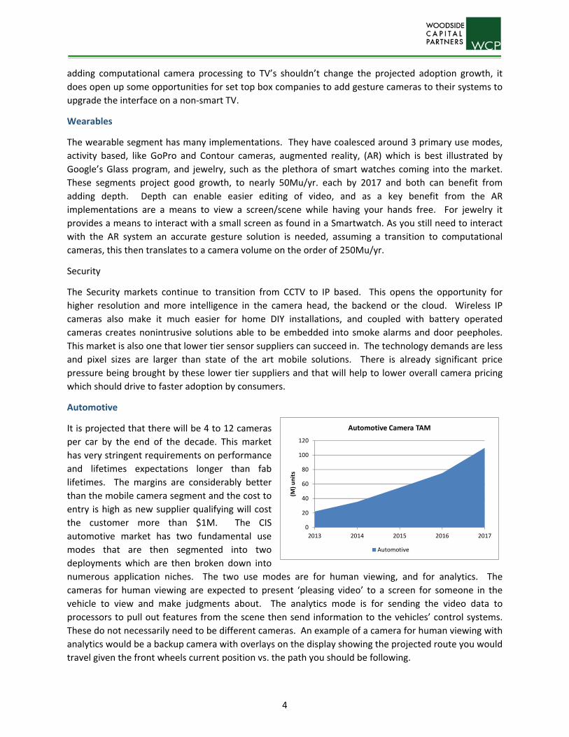
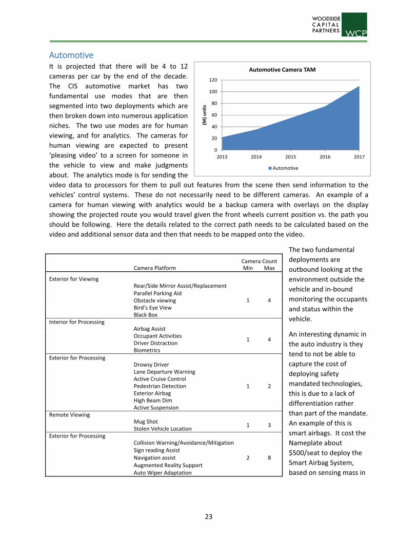
Automotive
It is projected that there will be 4 to 12 cameras
per car by the end of the decade. This market
has very stringent requirements on performance
and lifetimes expectations longer than fab
lifetimes. The margins are considerably better
than the mobile camera segment and the cost to
entry is high as new supplier qualifying will cost
the customer more than $1M. The CIS
automotive market has two fundamental use
modes that are then segmented into two
deployments which are then broken down into
numerous application niches. The two use modes are for human viewing, and for analytics. The
cameras for human viewing are expected to present ‘pleasing video’ to a screen for someone in the
vehicle to view and make judgments about. The analytics mode is for sending the video data to
processors to pull out features from the scene then send information to the vehicles’ control systems.
These do not necessarily need to be different cameras. An example of a camera for human viewing with
analytics would be a backup camera with overlays on the display showing the projected route you would
travel given the front wheels current position vs. the path you should be following.

5
Human Machine Interface
Human‐Machine Interface can be broken down into 2 sub‐segments, Human‐Device Interface, HDI, and
Smart Environments, SE. HDI’s focus is about people interacting with consumer goods, like TVs Laptops,
Phones and Tablets. It tends to be a more active interaction where the person is presenting themselves
to the device, and using gestures and body motions to control the device. SE tends to be a more passive
interaction and is about the space and or products interacting with a person, like lighting, HVAC, and
Surround Sound positional adaptation. According to Markets and Markets, the total gesture recognition
is expected to reach $22.04 billion by 2020 at a double digit CAGR from 2013 till 2020. The HDI space
broke out with the Wii, and expanded with the Kinect, it is now strongly emerging in cell phones. The SE
space is still in the concept stage waiting for processing to improve and pricing to come down. The
computational camera resources being deployed in the consumer space will address both of these
hurdles. There are few high volume camera implementations that are being deployed to provide a
significant return on investment. The SE space is however one that will be deployed specifically to
reduce power consumption, and improve a company’s bottom line.
Technology
There continues to be strong focus on improving the users experience by simultaneously driving to
improved low light performance and better dynamic range. The issue is many of the techniques being
developed require non‐standard processing. This presents problems to existing platform solutions like
the embedded ISP in application processors while simultaneously creating an opportunity for sensor
companies making ASICs and 3rd party processors. A considerable effort is being put forth on how to
efficiently add depth detection, and this could significantly affect the way users interact with their
images, as well as provide a significant leap in overall camera technology
Summary
The camera TAM numbers shown are based on an evolving growth model CAGR for the segment is
projected to be greater the 10% during this time period. Strong growth, overlapping functionality and
new markets are helping to keep the embedded camera strong for the foreseeable future. If
computational cameras are accepted the total volume of imagers and modules could be greater than
3.5Bu by 2017.
0
500
1,000
1,500
2,000
2,500
3,000
2013 2014 2015 2016 2017
(M) units
Embedded Camera TAM
Augmented Reality
Smart Home
Smart Office
Automotive
Security Cam
PC Cam/ Laptop
Gaming
Smart TV
Action Cam
Tablet
Smartphone
6
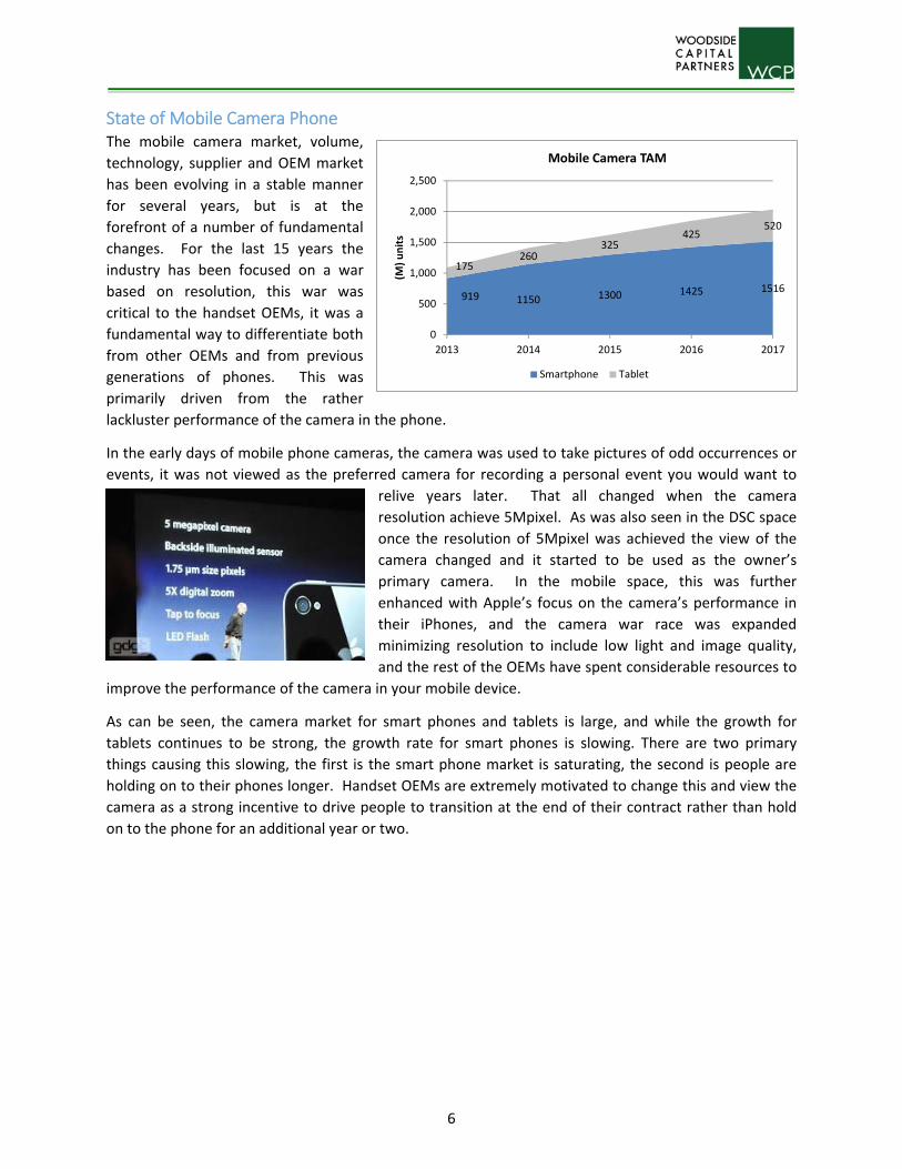
State of Mobile Camera Phone The mobile camera market, volume,
technology, supplier and OEM market
has been evolving in a stable manner
for several years, but is at the
forefront of a number of fundamental
changes. For the last 15 years the
industry has been focused on a war
based on resolution, this war was
critical to the handset OEMs, it was a
fundamental way to differentiate both
from other OEMs and from previous
generations of phones. This was
primarily driven from the rather
lackluster performance of the camera in the phone.
In the early days of mobile phone cameras, the camera was used to take pictures of odd occurrences or
events, it was not viewed as the preferred camera for recording a personal event you would want to
relive years later. That all changed when the camera
resolution achieve 5Mpixel. As was also seen in the DSC space
once the resolution of 5Mpixel was achieved the view of the
camera changed and it started to be used as the owner’s
primary camera. In the mobile space, this was further
enhanced with Apple’s focus on the camera’s performance in
their iPhones, and the camera war race was expanded
minimizing resolution to include low light and image quality,
and the rest of the OEMs have spent considerable resources to
improve the performance of the camera in your mobile device.
As can be seen, the camera market for smart phones and tablets is large, and while the growth for
tablets continues to be strong, the growth rate for smart phones is slowing. There are two primary
things causing this slowing, the first is the smart phone market is saturating, the second is people are
holding on to their phones longer. Handset OEMs are extremely motivated to change this and view the
camera as a strong incentive to drive people to transition at the end of their contract rather than hold
on to the phone for an additional year or two.
919 1150 1300 1425 1516
175260
325425
520
0
500
1,000
1,500
2,000
2,500
2013 2014 2015 2016 2017
(M) units
Mobile Camera TAM
Smartphone Tablet
7
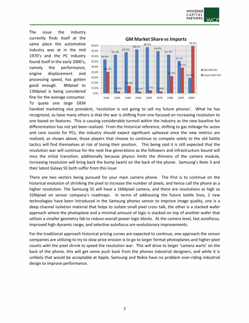
The issue the industry
currently finds itself at the
same place the automotive
industry was at in the mid
1970’s and the PC industry
found itself in the early 2000’s,
namely the performance,
engine displacement and
processing speed, has gotten
good enough. 8Mpixel to
13Mpixel is being considered
fine for the average consumer.
To quote one large OEM
handset marketing vice president, ‘resolution is not going to sell my future phones’. What he has
recognized, as have many others is that the war is shifting from one focused on increasing resolution to
one based on features. This is causing considerable turmoil within the industry as the new baseline for
differentiation has not yet been realized. From the historical reference, shifting to gas mileage for autos
and core counts for PCs, the industry should expect significant upheaval once the new metrics are
realized, as shown above, those players that choose to continue to compete solely to the old battle
tactics will find themselves at risk of losing their position. This being said it is still expected that the
resolution war will continue for the next few generations as the followers and infrastructure bound will
miss the initial transition, additionally because physics limits the thinness of the camera module,
increasing resolution will bring back the bump (wart) on the back of the phone. Samsung’s Note 3 and
their latest Galaxy S5 both suffer from this issue
There are two vectors being pursued for your main camera phone. The first is to continue on the
historical evolution of shrinking the pixel to increase the number of pixels, and hence call the phone as a
higher resolution. The Samsung S5 will have a 16Mpixel camera, and there are resolutions as high as
32Mpixel on sensor company’s roadmaps. In terms of addressing the future battle lines, 2 new
technologies have been introduced in the Samsung phones sensor to improve image quality, one is a
deep channel isolation material that helps to isolate small pixel cross talk, the other is a stacked wafer
approach where the photoplane and a minimal amount of logic is stacked on top of another wafer that
utilizes a smaller geometry fab to reduce overall power logic blocks. At the camera level, fast autofocus,
improved high dynamic range, and selective autofocus are evolutionary improvements.
For the traditional approach historical pricing curves are expected to continue, one approach the sensor
companies are utilizing to try to slow price erosion is to go to larger format photoplanes and higher pixel
counts with the pixel shrink to speed the resolution war. This will drive to larger ‘camera warts’ on the
back of the phone, this will get some push back from the phones industrial designers, and while it is
unlikely that would be acceptable at Apple, Samsung and Nokia have no problem over‐riding industrial
design to improve performance.

8
Disruption The fundamental design for the camera in your phone was developed in the
late 1600’s and while the core components have improved, the basic design
is the same. One could design the lenses for the camera phone from a book
published in the late 1800’s. To say this industry is ripe for disruption is
quite an understatement. The focus that shows the most promise is based
on the concept of computational cameras. At its core computational
cameras are based on getting multiple views of the scene either through
lens manipulation, Lytro, or by the use of multiple cameras as shown on the
right, CorePhotonics, Heptagon, Lynx, Pelican Imaging and Toshiba. This
produces a raw image that tends to look more like a bugs eye view than a
traditional view for human consumption. The other approach is to utilize one
sensor coupled with an active non‐visible lighting source to acquire depth and
overlay this depth map with a traditional camera’s data. This is what is done in the Microsoft Kinect
Platform. There are two main technology approaches to collect depth detail this way. The first is called
structured light. Here the light source outputs a pattern, the pattern of light reflects off of surfaces in
the scene and the now distorted reflected patterned image is captured on a standard image sensor then
processed to develop a depth map, PrimeSense, acquired by Apple, was the leading solution supplier for
this approach, the second approach is based on measuring the phase shift of light. Here specialized
pixels capture the phase of light after it reflects off a surface, as the phase of light captured is dependent
upon the distance traveled, the system can translate the results into a depth map of the scene which
can then be overlaid with a conventional camera.
A fundamental difference between the active
illumination approach and the multi‐camera
approach is what the depth map looks like.
From an active illumination approach the depth
is generated as shapes and blobs (depending
upon the resolution) of the objects. Flat and
non‐flat surfaces are created with equal
accuracy. However the overall depth map tends to be much lower than the color image resolution.
Additionally as active illumination is needed, this approach does not work well under sunlight, so is not
well suited for mobile phone platforms, but as there is active illumination it will work when there is
little, or no, ambient light. In practice the active
illumination approach has problems with objects
close (<0.3M) to the camera, and can only provide
depth as far out as the power of the light source can
drive. The accuracy of the depth map within its
range tends to be greater than 95% of the
distance between the object and the camera. Multi
camera solutions develop the depth map based on
parallax, this is similar to how your eye
finds depth,
9
triangulation on points of the scene between the imagers. This solution does not however provide a
depth point if there is no variation in contrast or color within a region of the scene. This means the
multi‐ camera approach produces an edge map, but cannot fill in the flat regions inside the edges. The
traditional approach is to utilizing the contrast and texture of the color image to fill in the missing detail
between the edges, this requires a second level of processing in addition to the parallax processing. This
approach is based on ambient light, so it works equally well indoors and out making it better for mobile
solutions, but if the light level is low it will not produce a depth map. The depth accuracy of a multi
camera approach is predicated by the baseline between cameras, the approaches considered for mobile
applications would have a significant fall off in accuracy beyond 3‐5 meters, this does not mean depth
could not be calculated beyond 5 meters, just that an object at 10 meters and another object at 15
meters may be within the same error range, so could be called out at the same distance. The
implication is if the cameras are close to each other as in a phone they would not be effective for
measuring the size of rooms, or for real scene AR gaming.
The promise of a depth map An image with a depth map enables numerous pre and post captures features. You can design an all in
focus optical lens system. Form the user’s perspective this means you will no longer capture out of
focus images, and do not have to wait for the lens autofocus system to settle before you can capture an
image. This should reduce first shot capture by 5‐10X from most existing solutions as well as reduce
shot to shot lag when trying to take a picture in far focus and then moving to close focus or vice‐versa.
The depth map can then be used to modify an image after capture to non‐destructively move the virtual
depth of field to any point in the scene, it can let you change the size of the depth of field as well as the
number of depths of field.
Post capture manipulation
If the depth resolution and subsequent point cloud is of high enough resolution you should be able to
isolate objects within a scene very easily (with your fingers on your phone). The promise of
computational cameras is that once you isolate objects you can now manipulate them by changing filter,
lighting, chroma, or focus effects. Imagine Instragram at the object level. You can also add objects and
have them scale correctly relative to their position, or delete objects, as well as move them forward or
backward in the scene. However, you will still not have any detail behind an object, so will either have a
‘hole’ or will need to duplicate the background. The object isolation function can be extrapolated to
digital cosmetics or enhancements, and the hook would be this would only take seconds to do prior to
posting an image. Additionally, if structured correctly, could enable your images to be easily
manipulated by friends and family on social media sites like Facebook. Currently your interaction with a
posted image is typically to hit the like button or post a twitter like comment, now you could have
serialized image manipulation without the need for learning how to use Photoshop, on your phone in
seconds you could make the changes and repost the image. There are several ways the social media
sites could leverage this capability financially.
In addition, being able to capture a high resolution image and high accuracy depth map will enable your
phone to render an object into a 3 dimensional avatar. Over the last 18 months several cameras have
been developed utilizing PrimeSense technology to render real objects for 3D printing, with Apple’s
purchase Primesense this market is in a bit of a panic.
10
Lenslet Approach
Lytro’s approach has been to insert a lenslet into the optical path in front of the camera
to provide thousands of small views of the scene each slightly shifted from the
neighboring view. From these views parallax is calculated which can then be translated
into a depth map. The benefit with this approach is that it can utilize the existing
infrastructure’s hardware components, and add its lenslet to the optical path. The issues
with this approach is it increases the height of the camera, and needs intensive specialized processing,
this approach is not called computational cameras for nothing. The first solution to market also suffered
from a very significant reduction in effective resolution. A 14Mpixel sensor was used and after their
processing the effective resolution was around 1Mpixel. While Lytro continues to improve, these three
issues have made it difficult to gain traction in any volume markets.
Array Camera Approach
Using numerous cameras to provide a view of the scene is generating interest in the mobile camera
space. The approaches seem to have coalesced into 2 variations, one variation utilizes super‐resolution
to take an array of lower resolution imagers and produce a higher resolution resultant image. The other
variation takes a small number of full resolution cameras with different fields of view (FOV) to produce a
resultant image that offer post capture optical zoom.
Multi‐Camera Super‐resolution approach
Pelican Imaging is one of the first companies developing the Multi‐Camera
Super‐resolution approach and claims very strong IP position. The initial
approach was to take an array of 16 imagers (4x4) on a single chip, each
with less than 0.75Mpixel resolution, and the associated array of lens
elements are each on a single 4x4 substrate to produce a high resolution image. The projected benefits
are that the camera module height is on the order of 50% to 60% of a conventional mobile phone
module, a high resolution depth edge map can be developed that is perfectly aligned with the color
image, and the smaller arrays enable a simplified lens design with a single standard I/O interface.
Additionally, there is considerable redundancy so the overall yield should be better than a conventional
imaging chip of the same size. This approach does have some issues, it requires a custom sensor and
lens assembly and the back focal tolerances are much tighter than is currently being built for any non‐
optical image stabilized modules. This means it will likely necessitate active alignment which requires
special assembly equipment and takes longer to assemble. Processing of the image data is very
specialized and is not well suited for the traditional application processor architectures, (computational
camera) this means a special processor or custom ASIC will likely be needed, which adds more cost. The
initial positioning of the current Pelican solution was intended to be 8Mpixel, assembled units are
producing results more in line with a 5Mpixel conventional camera, as the current 5Mpixel cameras
available are based on a 1/5” optical format the overall height difference between the Pelican and an
equivalent resolution camera is approaching parity.
Special sensor, special lens, special assembly, and an additional processing chip has the potential to
make this a much more expensive solution when compared to a conventional camera, the question that
is still unanswered is whether the overall value proposition of providing a high resolution depth map to
enable all the features mentioned earlier trumps the significant increase in cost. If Pelican is able to
achieve a 12‐16Mpixel effective resolution than a cost increase as high as 2x could be realistic.
11
Heptagon and Lynx are pursuing a 2x2 approach. There are numerous
other companies in the traditional supply chain starting to promote a
2x2 approach. Newport Imaging attempted this approach more than 15
years ago, and abandoned it, Sony bought and holds the Newport IP at this time. The 2x2 approach
utilizes higher resolution imagers, on the order of 5Mpixel or 13Mpixel, they are
also claiming to achieve full pixel count resolution (20Mpixel for a 2x2, 5Mpixel
solution). If they are able to achieve these types of resolutions it would be a very
significant breakthrough as conventional super‐resolution thinking is that they
should be not able to achieve the same resolution as the number of pixels
available. The benefits from this approach over the Pelican approach is that they are able to use off the
shelf imagers and lenses, they claim to be able to use the existing apps processors, and that the current
apps processors are powerful enough to maintain 1080P‐30 fps video. The overall cost should be close
to the higher resolution conventional solution, a 1.2‐2x ratio. They get depth with the associated
benefits listed, and the overall height is lower than the effective resolution they achieve. They will likely
need a chip to merge the numerous I/O's to feed into the processor. The issues with this approach are
associated with the problems from only having 4 imagers to work with. Most approaches being
proposed would have 1 traditional Bayer color filter configuration and the other three imagers would be
red, green or blue. This means you have the potential for regions of the image to be in a color shadow
of the imagers. As an example a picture of someone close to the camera may have one ear that limited
blue information and the other ear has limited red information because the front of your face blocks the
view of the side of your head from either the blue or red camera. If they are using red green and blue
imagers they will need to do special processing. Current feedback is that the image artifacts from this
approach are still significant enough to be considered not ready for the primary camera, however if
implemented as a front facing camera it would enable high accuracy gesture input, and the image
quality expectations of the front facing (screen‐side) camera are considerably lower than the primary
camera.
Stereo Cameras
Toshiba has developed a stereo camera solution with a pair of 5Mpixel imagers and
processing on the module. They claim they can achieve an effective 13Mpixel
resolution through super‐resolution and provide a VGA resolution depth map. They
are demonstrating the solution currently. The benefits to the stereo approach is
that is closest to the existing legacy implementations, it can utilize standard Bayer
for both sensors so can use the embedded image processing logic on most apps processors, this will
reduce overall power consumption and ease adoption and support from the apps processing companies,
and won’t suffer from the color shadowing problem. It will be thinner than a single module of
equivalent resolution after super‐resolution processing. The issues are associated with the lower depth
map resolution. This will make it more difficult to do any of the object level processing mentioned
earlier as the color resolution and depth resolution don’t match. Another issue is that stereo imaging
has been around since the 1800’s so the barrier to entry through IP is low and as one of the larger
players has already stepped in it is unlikely a smaller startup would be able to get significant traction.
Stereo Zoom
CorePhotonics is developing a stereo camera approach with a twist. One
of the two cameras has a smaller field of view than the other. This lets

12
175260
357.5
637.5
936
175260
325425 520
0
200
400
600
800
1,000
2013 2014 2015 2016 2017
(M) units
Tablet Camera TAMwith Computational Camera Adoption
Tablet (Computational Camera) Tablet
them provide optical 3x zoom either during or after capture, without the size issues associated with a
conventional moving lens zoom solution. The benefit to their approach is the zoom capability can occur
with off the shelf hardware components, and predominantly existing image processing. CorePhotonics
adds their own processing to align the data from the two cameras and has mentioned the ability to
provide smooth zoom between the two cameras.
It is also significantly less expensive than a
conventional zoom approach, and the overall
module thickness would be more than half the
thickness of a conventional zoom module. Issues
are that while it is thinner than a conventional
zoom approach to overall solution, it is still
thicker than a legacy non‐zoom mobile camera module. It will also be slightly more than twice as
expensive when compared to a non‐zoom module. The value proposition then rests on how important
the OEM camera groups believe zoom is
relative to the cost.
As shown, the impact of the mobile
market adopting computational
cameras would be very significant to
the market size, however as the
expectation is that individual cameras
would be of lower resolution the
revenue would grow at 50‐75% of the
unit growth. This could be problematic
to the investors as component suppliers
per unit ASP would actually decline
relative to continuing down the
conventional camera implementation. Another area to monitor related to multi‐camera adoptions are
associated with data bandwidth and the lag between a market shift, the market settling upon a technical
approach and the apps processing companies embedding the processing into their chip. Here companies
like Movidius may find themselves very
opportunistically positioned for a
multiyear bonanza as the approach
settles. One other thing to monitor is
wafer capacity, captive fab companies
like Sony and Samsung may find
themselves needing to make very
significant CAPEX investments to meet
demand. Single source contract fab
houses like Aptina, GalaxyCore, and
Pixelplus quickly find themselves putting
their customers on allocation, while
multi‐source contract fab companies like Omnivision may find themselves achieving a significant
windfall
1,150
1,430
2,138
2,729
919
1,300 1,425 1,516
0
500
1,000
1,500
2,000
2,500
3,000
2013 2014 2015 2016 2017
(M) units
Mobile Camera TAMwith Computational Camera Adoption
Smartphone (Computational Camera) Smartphone

13
Sensor/OEM Supplier Map
Computational Camera Suppliers
14
0
50
100
150
200
250
2013 2014 2015 2016 2017
(M) units
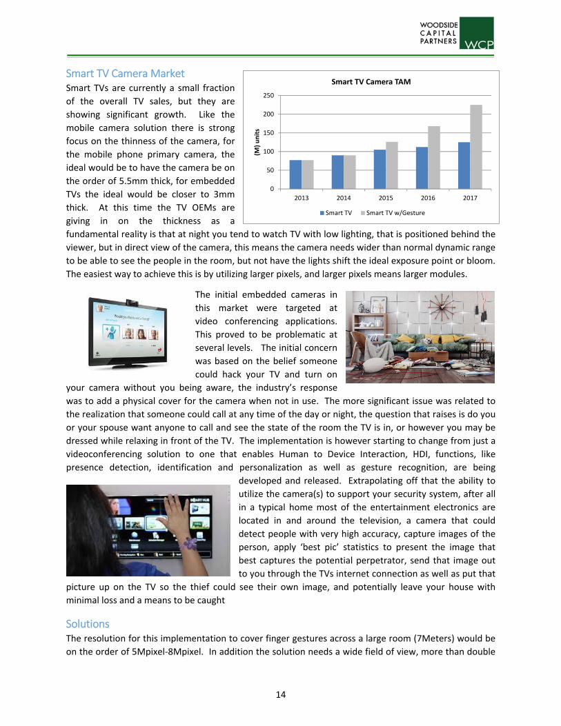
Smart TV Camera TAM
Smart TV Smart TV w/Gesture
Smart TV Camera Market Smart TVs are currently a small fraction
of the overall TV sales, but they are
showing significant growth. Like the
mobile camera solution there is strong
focus on the thinness of the camera, for
the mobile phone primary camera, the
ideal would be to have the camera be on
the order of 5.5mm thick, for embedded
TVs the ideal would be closer to 3mm
thick. At this time the TV OEMs are
giving in on the thickness as a
fundamental reality is that at night you tend to watch TV with low lighting, that is positioned behind the
viewer, but in direct view of the camera, this means the camera needs wider than normal dynamic range
to be able to see the people in the room, but not have the lights shift the ideal exposure point or bloom.
The easiest way to achieve this is by utilizing larger pixels, and larger pixels means larger modules.
The initial embedded cameras in
this market were targeted at
video conferencing applications.
This proved to be problematic at
several levels. The initial concern
was based on the belief someone
could hack your TV and turn on
your camera without you being aware, the industry’s response
was to add a physical cover for the camera when not in use. The more significant issue was related to
the realization that someone could call at any time of the day or night, the question that raises is do you
or your spouse want anyone to call and see the state of the room the TV is in, or however you may be
dressed while relaxing in front of the TV. The implementation is however starting to change from just a
videoconferencing solution to one that enables Human to Device Interaction, HDI, functions, like
presence detection, identification and personalization as well as gesture recognition, are being
developed and released. Extrapolating off that the ability to
utilize the camera(s) to support your security system, after all
in a typical home most of the entertainment electronics are
located in and around the television, a camera that could
detect people with very high accuracy, capture images of the
person, apply ‘best pic’ statistics to present the image that
best captures the potential perpetrator, send that image out
to you through the TVs internet connection as well as put that
picture up on the TV so the thief could see their own image, and potentially leave your house with
minimal loss and a means to be caught
Solutions The resolution for this implementation to cover finger gestures across a large room (7Meters) would be
on the order of 5Mpixel‐8Mpixel. In addition the solution needs a wide field of view, more than double

15
a mobile camera solution. The solution also needs to work from 20cm to at least 4Meters, ideally
7meters. It needs to see fingers move at all distances. So the x,y,z accuracy range needs to be on the
order of 1‐2cm across the entire range and field of view. This is non‐trivial, and currently only LIDAR
based solutions could achieve all of these metrics.
As this is primarily an indoor use case, both active illumination and multi‐camera solutions are viable. In
fact the Kinect system is based on active illumination technologies and has worked quite well for several
years, within a more constrained area of interest. However the current Kinect solution’s effective depth
resolution is just achieving 1Mpixel and has very low acuity with anything closer than 0.5Meters or more
than 4 Meters from the TV. One potential approach being considered is to merge a stereo camera
solution, which gives good accuracy in the near field, with a structured light active illumination solution
which gives better depth acuity, as well as combining the high resolution edge detection and blob
detection to minimize accurate object isolation processing.
If you can minimize the object isolation processing you enable a means to remove the background
(messy living room replaced with clean) and create an avatar representation of yourself when you are
presentable.
The camera resolution range is from 1080P to 5Mpixel, and will shift to 4Kx2k within the next three
years. The higher resolution is the minimum of what would be needed to resolve gestures at 7 Meters.
The chart above shows the conventional camera market size for embedded smart TV cameras and
‘upgrading’ a legacy TV with a multi camera gesture capable set top box with a non‐embedded camera.
The potential revenue growth rate would be 1.2‐1.4X greater than the gesture camera volume growth
rate as the gesture commands for a TV are given farther than for a smartphone or tablet and so the
camera resolution would need to be larger, not smaller as is expected in the mobile space. The
hardware component suppliers for gesture based cameras are the same as are outlined in the
computational camera supplier map in the previous section.
As shown in the aftermarket mapping several of the
smart TV suppliers are also supplying aftermarket
cameras in the expectation that as the smart TV takes off
legacy TV owners will want a means to mimic the
interaction. It is expected the current set top box
suppliers, Roku, Tivo, Google, Cisco, General Instruments
will follow suit by adding a gesture based solution,
More detail on the potential new interactions modalities
being enabled will be covered in the HDI section.

16
Smart TV Camera Map

17
0
10
20
30
40
50
2013 2014 2015 2016 2017
(M) units
Wearable Camera TAM
Action Cam Augmented Reality
Wearables
The wearable segment has many
implementations. They have coalesced
around 3 primary use modes, activity
based, like GoPro and Contour cameras
and augmented reality, which is best
illustrated by Google’s Glass program,
and jewelry, such as the plethora of
smart watches coming into the market.
Activity Based Cameras The activity based solutions are
essentially Camcorders with solid state
recording drives and cloud storage, they have found an interesting niche, and are unlikely to be
subsumed by your smart phone like what happened to Flip. The reason being that the activity cameras
are subjected to potentially being broken during the activity and people do not want to put their phones
at risk that way. The camera components are high end, with top of the line glass lenses and large pixel
HDTV wider dynamic range sensors. The camera modules and housings are engineered to withstand
high shock and vibration, and while this makes the overall footprint larger it has not impeded steady
adoption. The current implementations are based on
existing hardware and not pushing the technical
envelope. With the viral effect growth being
experienced by posted videos like the antelope
colliding with a bicyclist, it is expected that the larger
OEMs (GoPro, Contour) and the vertically integrated
OEMs (Sony, Panasonic, and Sharp) are developing
more custom sensors and optics. The wearer is not
actively viewing the scene during capture and so
cannot adjust the camera until after the event has
been recorded. It would also not be surprising that
before 2016 the activity based cameras providers would introduce a computational camera solution as a
means to reduce the overall camera size, and provide post capture manipulation of the video. Activity
based cameras should expect strong growth for the next 3‐5 years, but are likely to saturate in the latter
part of this decade or early part of the 2020’s
18
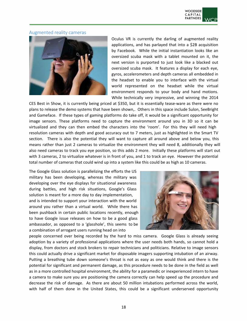
Augmented reality cameras Oculus VR is currently the darling of augmented reality
applications, and has parlayed that into a $2B acquisition
by Facebook. While the initial instantiation looks like an
oversized scuba mask with a tablet mounted on it, the
next version is purported to just look like a blacked out
oversized scuba mask. It features a display for each eye,
gyros, accelerometers and depth cameras all embedded in
the headset to enable you to interface with the virtual
world represented on the headset while the virtual
environment responds to your body and hand motions.
While technically very impressive, and winning the 2014
CES Best in Show, it is currently being priced at $350, but it is essentially tease‐ware as there were no
plans to release the demo systems that have been shown,. Others in this space include Sulon, SeeBright
and Gameface. If these types of gaming platforms do take off, it would be a significant opportunity for
image sensors. These platforms need to capture the environment around you in 3D so it can be
virtualized and they can then embed the characters into the ‘room’. For this they will need high
resolution cameras with depth and good accuracy out to 7 meters, just as highlighted in the Smart TV
section. There is also the potential they will want to capture all around above and below you, this
means rather than just 2 cameras to virtualize the environment they will need 8, additionally they will
also need cameras to track you eye position, so this adds 2 more. Initially these platforms will start out
with 3 cameras, 2 to virtualize whatever is in front of you, and 1 to track an eye. However the potential
total number of cameras that could wind up into a system like this could be as high as 10 cameras.
The Google Glass solution is parallelizing the efforts the US
military has been developing, whereas the military was
developing over the eye displays for situational awareness
during battles, and high risk situations, Google’s Glass
solution is meant for a more day to day implementation,
and is intended to support your interaction with the world
around you rather than a virtual world. While there has
been pushback in certain public locations recently, enough
to have Google issue releases on how to be a good glass
ambassador, as opposed to a ‘glasshole’, this seems to be
a combination of arrogant users running head on into
people concerned over being recorded by the hard to miss camera. Google Glass is already seeing
adoption by a variety of professional applications where the user needs both hands, so cannot hold a
display, from doctors and stock brokers to repair technicians and politicians. Relative to image sensors
this could actually drive a significant market for disposable imagers supporting intubation of an airway.
Putting a breathing tube down someone’s throat is not as easy as one would think and there is the
potential for significant and permanent damage, as this procedure needs to be done in the field as well
as in a more controlled hospital environment, the ability for a paramedic or inexperienced intern to have
a camera to make sure you are positioning the camera correctly can help speed up the procedure and
decrease the risk of damage. As there are about 50 million intubations performed across the world,
with half of them done in the United States, this could be a significant underserved opportunity
19
leveraging the heads up display technology. Numerous other startups and established consumer
products companies are developing their own version of Google Glass, this includes; Sony and Samsung.
Jewelry The jewelry segment is dominated by Smartwatches. This market is currently suffering from large bulky
appliances that are seeing some uptake by early adopters, and current thinking is that the market SAM
will be on the order of 20% of the Smartphone market (300Mu in2017). The initial generation of
watches had a camera embedded in them, as it was shown to be difficult to align your arm to take a
picture, the cameras are being removed. However the Smartwatch has a fundamental problem, if you
make the screen small enough to be fashionable you have also made it too small for someone to be able
to select icons on the touch screen. Most of the reviews on recent watches point out how hard it is to
move from screen to screen, the solution to this problem could be to utilize gestures rather than
actually touching the screen. The physical implementation would be similar to what is described
previously, except since the range of detection would be less than 0.3M, the effective resolution for the
cameras would need to be only 100K pixels or so. Power becomes the biggest hurdle for
implementation, and as power consumption is a focus for the sensor companies developing gesture
based imagers, this is a tractable problem that could be minimized within the next 18months. As this
implementation does not yet exist it has not been included in the market size graph, but would be
expected to follow a traditional Moore’s new tech adoption cycle, starting with the innovators at 1% of
the Smartphone market moving to the early adopters in the second year and growing to 3% of the
Smartphone market, then seeing rapid acceptance by the early adopters and achieving 10‐12% of the
smartphone market around years 4‐5 of release, followed by slowing growth after 5‐7 years. The
question is, when will all of the pieces come together in a viable highly accurate gesture interface way to
initiate this cycle?
20
Security A CMOS image sensor are expected to enjoy a CAGR of about 17% for the next 5 years as the industry
transitions from CCD to CMOS and as the IP Camera segment continues to grow and expand into home,
infrastructure and small business security.
One of the primary benefits of IP Cameras
over CCTV is the reduced need to run
dedicated video transfer lines. For a CCTV
installation a coax cable needs to be run from
the camera back to the recording location.
Running these lines takes a large amount of
the overall installation budget which
historically reduced the number of cameras
that could be purchased. With IP cameras, the
IT department has already run the CATx
cabling, so more money is available to
increase the number of cameras purchased. If
a situation arises where it is still difficult to
access an IP line, wireless IP data transfer is an
option.
Security camera solutions are characterized by
larger sized pixels with low to medium
resolution, VGA – 5Mpixel. Here size matters,
in the opposite way to the mobile market.
Just seeing cameras present, whether working or not will accomplish its goal of deterring crime, and the
much larger footprint allows for much larger sensors and lenses. While the industry is spending a
tremendous amount of resources trying to develop a submicron pixel for Mobile cameras, in the security
segment the pixel sizes are more on the order of state of the art in the early 2000s (6um‐3um). That is
not to say the technology from that time period is being used. The current security solutions finds itself
as a segment to try out new technologies or processes without the burden of also making the solution fit
into a small pixel. Technologies like piecewise linear response to extend dynamic range, greater than
real time frame rates and image stabilization were all introduced through the security market segment
before transitioning to higher volume smaller form factor consumer segments.
One of the primary differences between CCTV implementations and IP is that CCTV is still based on some
version of the NTSC/PAL format, while the IP cameras tend to be HD format. This had created a natural
barrier between the two segments, but CMOS performance and focus on the segment by companies like
Aptina and Omnivision has helped to start to enable using the same sensor, able to support either
format across both segments, as this trend continues it will accelerate the market shift from CCD to
CMOS Imaging.
The other significant difference between this market and consumer markets is the need for
performance in the Near Infrared (NIR) spectra. This light spectrum is beyond the human’s visible acuity
but silicon will respond to it. Consumer applications need to make sure these frequencies are blocked
from the sensors they will affect color quality, whereas for security, the expectation is that the sensor

21
will work under daytime conditions producing high quality color video,
and at night the camera will turn on a bank of NIR LEDS to illuminate
the scene without producing visible light so the camera can work
under any lighting conditions. Sensor companies are working on a
number of ways to address this issue, and once a satisfactory solution
is developed it should be expected to be transitioned to consumer
products. The benefit on the consumer side is the potential to extend
low light color by up to 2 f‐stops, provide non‐visible flash, and have
the camera mimic the eye in terms of having pixels act more like the
rods and cones in your eye.
As IP camera deployment grows a new problem is starting to be realized, the cameras are stealing
available bandwidth for the day to day operations of the company, and while currently few are seeing
this as an issue the problem will grow. One way to get around this issue is to only have the cameras
sending video data when an event is occurring in the scene. The processing will need to be in the
camera and will need to have a high reliability factor. This presents a strong growth opportunity for
video analytic companies and mid to low end general purpose processing and SP chip companies. Being
able to improve the analytics accuracy would be aided with the deployment of higher resolution and
depth based cameras, so the same technologies being developed to improve the user experience on
mobile phones can be or already has been deployed in the security camera segment.
While CMOS is seeing strong growth, the overall commercial security camera market’s growth is
approaching anemic. DIY wireless IP based home security is opening up a saturated market, however
DIY home security has a fundamental problem. Ideally the camera is placed within a foot of the ceiling
to assure good coverage and minimize objects blocking its view. Power for this camera however tends
to be located a foot from the floor. The problem is, do you or your spouse want a cable running up the
wall from the outlet to the camera. 10 years ago a company called AVAAK attempted to solve this issue
by developing a battery operated camera that only worked when some other traditional home security
sensor, glass break, pressure pad, or PIR, activated the camera. While it was a means to address the
problem, the company for other reasons never took off. This approach is now starting to be applied to
embedding in smoke alarms, door or window sensors, or motion detectors. Another approach currently
being sold is embedded into motion sensing outdoor lighting. This is a natural location for the camera
and the interface is either wireless IP or power line modem. In most of the DIY segment, cost and power
are much stronger drivers than high end features like high dynamic range. That being said low light
performance is still a critical technical requirement across both the commercial and consumer market
niches.
As mentioned in the Smart TV section the camera embedded into the TV could show a thief his own
‘mug’ shot to try to induce him to leave with minimal damage done to your home, in a similar manner
home networked cameras could be set up to automatically present a picture to your TV in addition to
your phone, tablet, PC and monitoring service whenever activated.
An interesting anecdotal trend beginning to take hold is homeowner’s allowing local police departments
direct access to their home security camera’s live streams, the thought being the police can get better
access to local information for higher crime areas or tracking people and vehicles as they traverse
22
through a town or neighborhood. To date it is been considered reciprocal in that you would improve
the police response on an event to better than a monitoring company.
As mentioned earlier this space does not drive small pixel technology so it has been a point of entry for
several companies looking to enter the CMOS imaging sensor space, companies like GalaxyCore, and
Pixelplus leveraged their early lower performance low end products into revenue to drive their
development of more advanced technologies and are now reaping that reward as they work to displace
the existing suppliers in the low end of consumer cameras like front facing mobile cameras and
embedded PC cameras.
The average DIY installer has little knowledge about camera placement and tends to go through a series
of camera repositioning as they realize a camera that alerts whenever someone walks up to a front door
will also alert whenever a car drives down the street, or where the cat can sit in front of the camera.
This is why the ability to process the scene to pull out features and activities of interest is increasing in
importance. Basic analytics that just do frame differencing and to alert if a particular volume of the
region changed from frame to frame is the norm for the current home security cameras. This has
proven to be a poor method for alerting, as the user would tend to turn down the response sensitivity
for all but the most basic scenes to reduce false alerts, to a point where the camera’s performance was
not really useful.
DropCam is one company that is getting around the cost of adding a powerful enough processor in the
camera to do effective detection. Their approach is to stream the video to the cloud where it is
processed, you pay a monthly subscription service to process and store the video stream. One camera
consumes more than 50GB of internet bandwidth per month and given the monthly bandwidth usage,
deploying multiple Dropcams would likely also cause the user to have to upgrade their Home IP service.
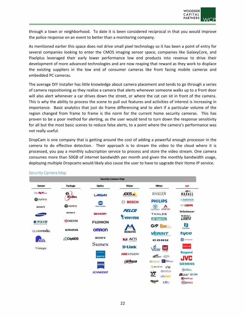
Security Camera Map
23
0
20
40
60
80
100
120
2013 2014 2015 2016 2017
(M) units
Automotive Camera TAM
Automotive
Automotive It is projected that there will be 4 to 12
cameras per car by the end of the decade.
The CIS automotive market has two
fundamental use modes that are then
segmented into two deployments which are
then broken down into numerous application
niches. The two use modes are for human
viewing, and for analytics. The cameras for
human viewing are expected to present
‘pleasing video’ to a screen for someone in
the vehicle to view and make judgments
about. The analytics mode is for sending the
video data to processors for them to pull out features from the scene then send information to the
vehicles’ control systems. These do not necessarily need to be different cameras. An example of a
camera for human viewing with analytics would be a backup camera with overlays on the display
showing the projected route you would travel given the front wheels current position vs. the path you
should be following. Here the details related to the correct path needs to be calculated based on the
video and additional sensor data and then that needs to be mapped onto the video.
The two fundamental
deployments are
outbound looking at the
environment outside the
vehicle and in‐bound
monitoring the occupants
and status within the
vehicle.
An interesting dynamic in
the auto industry is they
tend to not be able to
capture the cost of
deploying safety
mandated technologies,
this is due to a lack of
differentiation rather
than part of the mandate.
An example of this is
smart airbags. It cost the
Nameplate about
$500/seat to deploy the
Smart Airbag System,
based on sensing mass in
Camera Count Camera Platform Min Max
Exterior for Viewing Rear/Side Mirror Assist/Replacement
1 4 Parallel Parking Aid Obstacle viewing Bird’s Eye View Black Box Interior for Processing Airbag Assist
1 4 Occupant Activities Driver Distraction Biometrics Exterior for Processing Drowsy Driver
1 2
Lane Departure Warning Active Cruise Control Pedestrian Detection Exterior Airbag High Beam Dim Active SuspensionRemote Viewing Mug Shot
1 3 Stolen Vehicle LocationExterior for Processing Collision Warning/Avoidance/Mitigation
2 8 Sign reading Assist Navigation assist Augmented Reality Support Auto Wiper Adaptation
24
the seat. The average y/y price increase for the year the Smart Airbag was deployed was closer to $200.
This means the OEM took an $800 margin hit on each car thy sold that year.
The US has mandated that every new car model shipped after June 2018 will include a backup camera
and display in the vehicle. GPS/Backup Camera options are currently priced in the $1000‐$2000. The
projected cost per vehicle will be on the order of $150 to do this deployment. The benefit that can be
realized with camera based safety systems is that a single camera platform can provide multiple
applications. The mandate is just to show the scene behind the vehicle, but upgrade options can include
the overlay option listed above, back over warnings, pre‐rear end collision prep, and automated parking
assistance. Given the markup already being realized for a backup camera, recouping the cost of the
deployment and leveraging the mandate to increase the per vehicle price is a viable opportunity for
each Nameplate.
The initial deployments were VGA
resolution, and the trend is shifting
from 720P up to 5+Mpixel depending
upon the application. While it is long
and painful, current qualified
suppliers enjoy a strong barrier to
entry. This is the hardest
environmental condition
requirements the volume CIS
suppliers will need to meet. The best
way to describe this segment’s
performance requirements is to
expect to design to Mil Spec
standards, but at pricing much closer
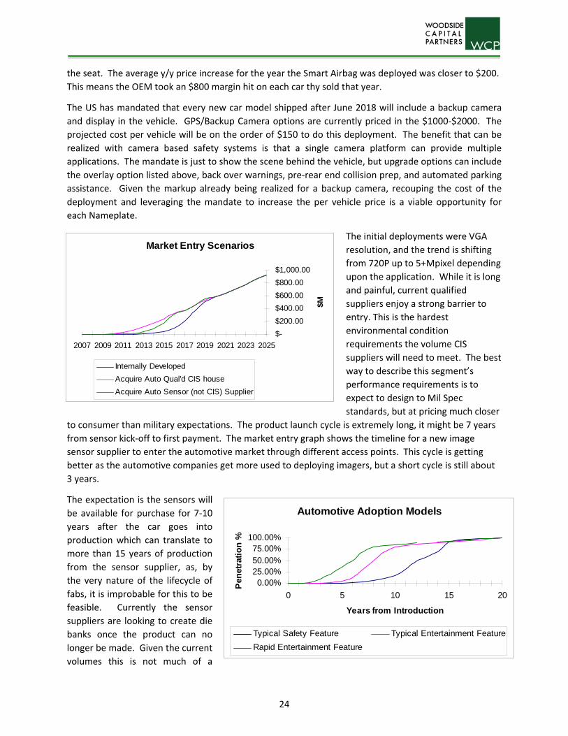
to consumer than military expectations. The product launch cycle is extremely long, it might be 7 years
from sensor kick‐off to first payment. The market entry graph shows the timeline for a new image
sensor supplier to enter the automotive market through different access points. This cycle is getting
better as the automotive companies get more used to deploying imagers, but a short cycle is still about
3 years.
The expectation is the sensors will
be available for purchase for 7‐10
years after the car goes into
production which can translate to
more than 15 years of production
from the sensor supplier, as, by
the very nature of the lifecycle of
fabs, it is improbable for this to be
feasible. Currently the sensor
suppliers are looking to create die
banks once the product can no
longer be made. Given the current
volumes this is not much of a
Market Entry Scenarios
$-
$200.00
$400.00
$600.00
$800.00
$1,000.00
2007 2009 2011 2013 2015 2017 2019 2021 2023 2025
$M
Internally Developed
Acquire Auto Qual'd CIS house
Acquire Auto Sensor (not CIS) Supplier
Automotive Adoption Models
0.00%25.00%50.00%75.00%
100.00%
0 5 10 15 20
Years from Introduction
Pen
etra
tio
n %
Typical Safety Feature Typical Entertainment Feature
Rapid Entertainment Feature
25
problem, however there could be significant cost and risk exposure as the volumes increase, if not
managed correctly.
When considering all these issues, why are certain sensor suppliers very focused on this market? There
are two primary reasons, the first is the margins, they are on the order of 2‐3 times the margins for
consumer products, as the volumes increase this will shrink but it should still be 1.5‐2X higher than
consumer products. The second is long term stable supplies, the ongoing cost of sales is quite low as
once you are designed into a socket it is almost impossible to get you designed out. This also means the
Tier 1 and Nameplates will forgo pricing to assure the supplier is stable. This is helping to keep out the
low end suppliers that are currently undermining margins in the security and front facing mobile camera
segments.
There are specific performance and environmental specifications that all but assure a sensor designed
for consumer markets will not accepted into the automotive market. The more typical way to ride the
long production approval cycle is to design the sensor for automotive then bring it to other markets, like
security, and industrial versions of consumer products.
The market entry scenarios shown above highlight how long it takes to get to design wins and stable
growth within the market. New supplier qualifications cost a tier 1 integrator over $1M. Over the last
15 years the nameplates (OEMs) have spent considerable effort reducing their supplier base by over
10x. Coupling these two facts together gives a significant advantage to Omnivision and Aptina, and
given Aptina’s recent issues in some of the larger consumer markets, their current penetration in the
automotive market may make them an ideal candidate for one of the other sensor companies that are
trying to get into automotive, or a tier 2 supplier like Gentex or Omron who is looking to establish a
more vertical position within the automotive camera market.
Channel Roles: » Nameplate
• OEM • Hyundai, Toyota, Ford . . . • Develops some technology • Tracks technology developments • Issues RFQs
» Tier 1 • Major component assembler • Delphi, Magna, Bosch, Hella, Aisin Seiki . . . • Develops and Assembles major components • Responds to Nameplate RFQs as well as sells new technologies up • Heavy technology development • Currently building cameras in‐house
» Major customer for image sensors » Tier 2
• Sub component assembler • Clarion, Gentex, Omron • Tends toward specialty focus • Will over time become the camera manufacturer
» Future primary customer for image sensors
26
One thing that does need to be considered for this market is exposure to liability. Some Sensor
suppliers have been adding internal checks and in‐chip temperature monitoring to their automotive
sensors, and the newer performance standards will mandate these features. Many of the applications
utilizing cameras are associated with the safety systems, if a wrong decision is made, someone will be
held liable. The initial reason for adding these features was to minimize liability exposure, if the sensor
supplier can show their component is only providing data, and they have implemented the means to
make sure the analytics can be assured the data is valid, they are in a strong position to make the case
to be removed from any lawsuits. The companies with significant exposure are the software, dedicated
hardware and tier 1 companies, and they are the ones who are analyzing the video data and sending
commands to the vehicles control systems.
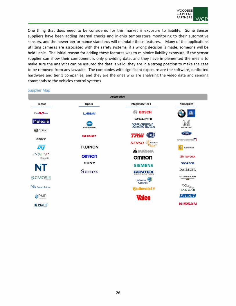
Supplier Map
27
Human‐Machine‐Interface ‐ HMI Human‐Machine Interface can be broken down into 2 sub‐segments, Human‐Device Interface, HDI, and
Smart Environments, SE. HDI’s focus is about people interacting with consumer goods, like TVs Laptops,
Phones and Tablets. It tends to be a more active interaction where the person is presenting themselves
to the device, and using gestures and body motions to control the device. SE tends to be a more passive
interaction and is about the space and or products interacting with a person. Things like lighting, HVAC,
Surround Sound positional adaptation.
HDI According to Markets and Markets, the total gesture recognition and touch‐less sensing market is
expected to reach $22.04 billion by 2020 at a double digit CAGR from 2013 till 2020. The market value in
2012 was approximately $2.2 billion. The HDI space broke out with the Wii, and expanded with the
Kinect, it is now strongly emerging in cell phones. There are already solutions available to track your
gaze and interacting with gestures, albeit with less than pleasing accuracies. This is done by using the
existing low resolution camera on the front (screen) side of your phone. An issue with this approach is
the power. The implementation to track gaze or gestures is run in SW on the Apps processor. This
means the camera is fully on pushing data down to the processor, which is using a non‐trivial amount of
resources to process the image and drive the commands for the phone to react, and all of this is
happening while your phone is sitting not being used on your desk. Sensor manufacturers are
addressing this by designing special modes for the sensor when the device is put into one of these
modes, but this is at best a band aid while the architecture evolves.
The focus now is to improve the accuracies, and realistically scene depth understanding is viewed as the
solution. The next focus will be on reducing the overhead, improving efficiency and positioning the
processing on a dedicated ASIC, or the sensor, in the camera.
The same approaches to add depth to the primary camera mentioned in the mobile phones section is
also being applied to the front facing camera. 1x2, 1x3 or 2x2 camera arrays are being developed to
Single/Stereo Software • eyesight (Israel) • SoftKinetic (Belgium) • PointGrab (Israel) • CrunchFish (Sweden) • Gestigon) • Imimtek (USA)
Silicon • Intel PCG (Israel)
• Intel Perceptual Computing (USA) • Microsoft (USA, UK, Israel) • Inuitive (Israel) • Google (USA) • Nvidia (USA), Movidius (USA)
Eye Tracking • EyeFluence (USA) • Tobii (Sweden) • SensoMotoric (Germany) • The Eye Tribe (Denmark) • Smart Eye (Sweden)
Depth Sensing • LeapMotion (USA) • Pebbles (Israel) • Mantis Vision (Israel)
• SoftKinetic (Belgium)
Smart Camera Processing Companies
28
enhance the interaction with the user by providing presence and gaze detection, gesture recognition,
and on the fly background subtraction. These screen side cameras architectures can be designed to
support phones, tablets, laptops and TVs by either increasing the separation between the cameras to
increase the depth accuracy farther from the device, and/or adding more cameras and super‐resolution
to address the need for better x‐y resolving capability at farther distances from the camera. A critical
component to this segment is size constraints in both the z and y dimensions. The z constraint is to
minimize the device thickness, the target would be to have a module at less than 3mm thick, the y
constraint is because all of the OEMs want to maximize the size of the screen and minimize the size of
the frame. This means companies focusing on a 2x2 or larger array architecture may find themselves
hard pressed to gain sockets on the screen side of the camera, because they have a larger y dimension.
The expectation is they may see some initial wins, if their performance is markedly better than a 1 by X
architecture, but over time they will either have to shift to a 1 dimensional array or be pushed out.
HDI Supplier Map
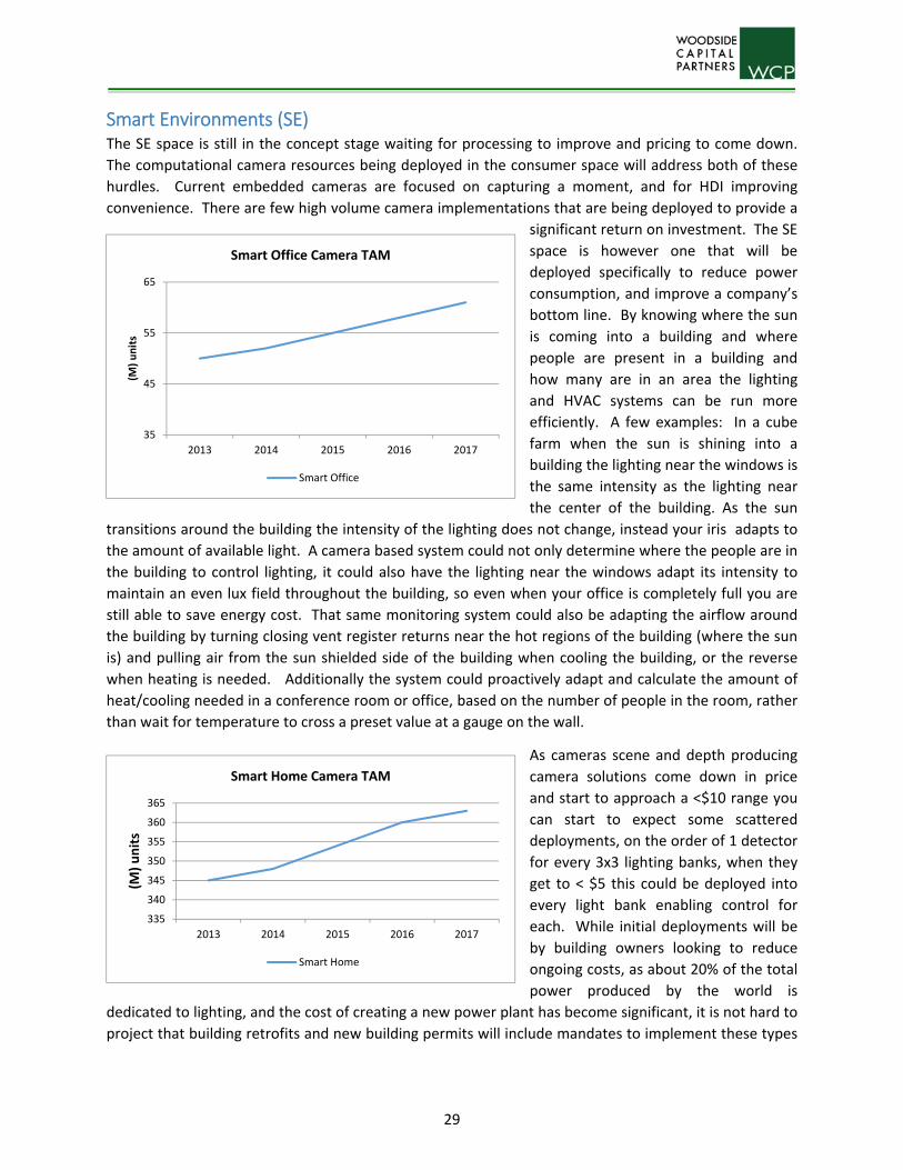
29
Smart Environments (SE) The SE space is still in the concept stage waiting for processing to improve and pricing to come down.
The computational camera resources being deployed in the consumer space will address both of these
hurdles. Current embedded cameras are focused on capturing a moment, and for HDI improving
convenience. There are few high volume camera implementations that are being deployed to provide a
significant return on investment. The SE
space is however one that will be
deployed specifically to reduce power
consumption, and improve a company’s
bottom line. By knowing where the sun
is coming into a building and where
people are present in a building and
how many are in an area the lighting
and HVAC systems can be run more
efficiently. A few examples: In a cube
farm when the sun is shining into a
building the lighting near the windows is
the same intensity as the lighting near
the center of the building. As the sun
transitions around the building the intensity of the lighting does not change, instead your iris adapts to
the amount of available light. A camera based system could not only determine where the people are in
the building to control lighting, it could also have the lighting near the windows adapt its intensity to
maintain an even lux field throughout the building, so even when your office is completely full you are
still able to save energy cost. That same monitoring system could also be adapting the airflow around
the building by turning closing vent register returns near the hot regions of the building (where the sun
is) and pulling air from the sun shielded side of the building when cooling the building, or the reverse
when heating is needed. Additionally the system could proactively adapt and calculate the amount of
heat/cooling needed in a conference room or office, based on the number of people in the room, rather
than wait for temperature to cross a preset value at a gauge on the wall.
As cameras scene and depth producing
camera solutions come down in price
and start to approach a <$10 range you
can start to expect some scattered
deployments, on the order of 1 detector
for every 3x3 lighting banks, when they
get to < $5 this could be deployed into
every light bank enabling control for
each. While initial deployments will be
by building owners looking to reduce
ongoing costs, as about 20% of the total
power produced by the world is
dedicated to lighting, and the cost of creating a new power plant has become significant, it is not hard to
project that building retrofits and new building permits will include mandates to implement these types
335
340
345
350
355
360
365
2013 2014 2015 2016 2017
(M) units
Smart Home Camera TAM
Smart Home
35
45
55
65
2013 2014 2015 2016 2017
(M) units
Smart Office Camera TAM
Smart Office

30
of power reduction requirements. Florida Power and Light is already implementing a smart lighting
infrastructure starting with street lights. They are piggy backing the installations for presence sensors
and networking on the back of switching out high power lights with LEDs. Once they can show the
reduced power requirements it is expected this will be deployed across the country and then the world.
Google has gone on a bit of a shopping spree acquiring several robotic and industrial machine vision
companies. While they have publicly touted they are looking at Robotics apps, they recently announced
its Tango Project, and this program can leverage many of the acquired company’s expertise. The intent
is to ‘give’ mobile devices a human‐scale understanding of space and motion. In essence a human to
device to environment approach. The platform is a modified smart phone. It has 3 image sensors, a
normal main camera, a low resolution camera for motion tracking, and depth sensing camera. It also has
2 dedicated Computer Vision Processors. This focus has very strong potential to drive the expansion of
both the HDI and the SE markets. If you look at this opportunity space you see that 2 of the three legs
of the stool are in place. The first leg is the hardware; sensors, processors, bandwidth and human
engagement are at or near the right performance levels to start seeing adoptions. This is not to say
there is room for significant improvements and changes in approach. The next leg is price; smart
phones have and continue to hold or drive down price while seeing generational improvements in
hardware performance. The final leg is scene processing, (software). Here there is room for significant
improvement, and while each of the small companies Google has acquired is capable of doing truly
excellent scene analysis and processing, they have had 2 limitations. The first is they were mostly living
hand‐to‐mouth doing custom programs for high NRE that were developed on dedicated industrial
platforms. The second is they were not large enough to drive modifications to processors such as how a
processing chip routes its data to enable the software to utilize DSPs CPUs and GPUs without having to
write to external memory between each transfer. Now with Google the experts from the acquired
companies have the opportunity to ‘request’ Qualcomm, Intel and nVidia to come to the Google office
to be ‘told’ what will be needed in future architectures.
A fundamental problem in the processing space as it relates to imaging is pattern matching. Pattern
matching in a CPU is very inefficient, especially as it relates to matching a single object to a large
database of potential matches. Your brain pattern matches against like type object in a massively
parallel way. With the current architectures this cannot be done efficiently, and so there is an
opportunity for companies developing new architectures capable of massively parallel pattern matching.
What is meant by this is not just running a large number of CPU cores in parallel, as that would produce
an unacceptable increase in power, but new architectures that are not based on traditional CPU
architectures.

31
SE Supplier Map

32
Technologies
Embedded Imaging Ecosystem
Embedded Imaging Ecosystem

33
Traditional Sensor Evolution
High Dynamic Range
Smaller and smaller pixels means lower signal carrying capacity for each pixel, which means lower
dynamic range, from a functional perspective this means more and more of the brighter regions in a
scene get saturated (the sky looks white instead of blue). To minimize this, sensor companies are
coming up with numerous approaches to extend the dynamic range. The technique currently in the
market is based on taking 2 or 3 frames each with a longer integration time, the short integration time
captures the bright regions of the scene, but leaves the rest under‐exposed whereas the long integration
saturates on the bright regions of the scene but captures the low illuminated regions. The better
exposed regions from each of the images are then combined to form a resultant image. There are issues
with this approach. As you are capturing images at different times (one after the other) things moving
at high speed in the scene are captured in different positions, and the resultant recombined image can
have interesting artifacts. Images have been captured where people blinked during the capture and in
the recombined image that person had a double set of eyelashes. This techniques does not work at all
when the camera is on a moving platform so cannot be used for automotive applications.
Other techniques are being developed based on changing the traditional linear response curve within
the pixel to either a logarithmic response or having a high conversion for low light that pivots to a lower
conversion if the charge in the pixel reaches a set intensity. This is called a dual conversion gain pixel.
Auto‐Focus (AF) Support
Newer sensors are being designed to support faster AF, one technique is to non‐destructively readout
small groups of pixels spread throughout the sensor between readout frames to assure focus is being
maintained, or to just readout this smaller set of pixels at a much faster frame rate to speed up the time
it takes to find initial focus or deal with rapid shift from far to close images. This approach can speed up
the time it takes for the camera to settle on a focal point by 2‐5X over a conventional approach.
Another technique is referred to a phase detection auto‐focus or PDAF. PDAF covers certain pixels with
a light shield that covers the left half of each pixel, and an equivalent number of pixels have their right
half covered, when the light reaches these two pixels, if an object is in focus, light rays from the extreme
sides of the lens converge right in the center of each sensor (#2 in the illustration below) Both pixels
would have identical images on them, indicating that
the object is indeed in perfect focus. If an object is out
of focus, the light would no longer converge and it
would hit different sides of the sensor, as illustrated
below, #1 shows the focal point too close, #2 in the right
position, #3 is too far and #4 way too far. This
technique has already been implemented into DSLRs
and is begin implemented into the Samsung S5. This
technique will allow very fast focusing, Samsung is
claiming 0.3s to focus. There are some potential issues with implementing this technique into cell
phone cameras though. DSLR lenses are much larger than mobile cameras, as this technique is based on
using the light rays coming from the left and right side of the lens to set focus, a small lens produces the
same problems highlighted with detecting depth on array cameras, namely the smaller the distance
between the two points the faster you depth accuracy falls off the farther you are from the camera.
34
This means the technique when applied to cell phones may help get ‘close’ to the right lens step, but
may still need some supplemental processing to reach the right final point. The other issue, also
highlighted in array cams is that it only finds edges if you are looking at a flat field you have no data to
compare the correct depth position. This means you need to have a large number of pixels half covered
to assure you ‘catch’ the edges in the scene, as each of these pixels have been compromised you either
have to treat them like defective pixels and remove them from the processing, or you have to gain up
the signal, and noise, to balance these PDAF pixels response. As it is being implemented into the
Samsung Galaxy S5 the technology has gone through extensive testing, and it should be expected to be
adopted by the industry at large within the next 18 months.
New Sensors
Array Cameras
Array sensors are described in the mobile section. They utilize
numerous imagers each with its own optics to reduce the
thickness of the module and enhance the information gotten
from a scene. They typically take 2, or more, lower resolution
imagers and through a technique called super resolution,
produce a higher resolution effective image. Certain
companies are claiming they can achieve the same effective
resolution as the resolution of all the pixels, or more, from all
the sensors (4 5Meg sensor produce a 20 Meg image). Toshiba has claimed they can achieve an
effective resolution of 13Meg from 2 5Meg imagers. This claim seems to go well beyond what the
technology has achieved to date, and so would need real world validation. Regardless, the ability to
reduce the overall thickness of the camera module has garnered significant interest from the handset
OEMs and there will be array camera smartphones in the market possibly as early as late 2014. A
driving force behind the adoption is by combining lower resolution sensors to achieve a higher
resolution effective image, you can either produce a higher resolution solution with the same module
thickness as the single camera, 2‐4 13Mpixel cameras with a z height of 5.2mm to produce a camera
with a resolution on the order of 20+ Mpixels, or use several lower resolution sensors (as Toshiba is
doing to achieve the same resolution as is commercially available, the benefit being you can reduce the
module z height by about a millimeter. 2‐4 8Mpixel sensors with a module height a 4‐4.5mm are being
touted to be able to produce a 13‐16Mpixel solution that in a single sensor camera would be 5.2‐6mm.
CorePhotonics has developed both the solution described above with a 2 camera approach as well as
another approach that has the 2 cameras have different fields of view. They then process the images
to give a solution with 3X optical zoom. The benefits to this zoom approach is the module is much
smaller than any zoom modules developed for cell phones, it is mechanically stable which is also a
problem for cell phone zoom modules and there is no loss of sensitivity (light being transferred through
the lens) as you zoom, which is a problem for all zoom cameras.
The camera ecosystem is not ready for this shift. In most cases the cameras are using a combination of
the standard Bayer color pattern as well as red green, blue and/or clear filtered sensors. This means the
processing is all done in software so in addition to having to deal with the increased power needed to
process a higher pixel count, the power budget is also being strained by not being embedded into
hardware. It is expected that 2 camera modules should be able to do all of their processing within the

35
acceptable apps processor power budget, but 4 or more cameras will most likely need a co‐processor.
Additionally there is no one stop shopping point for the OEMs. The sensors, optics and modules need to
be built to the specifications needed by each of the software processing companies, meaning all of the
current solutions are semi‐custom. The risk to the sensor companies is low, typically changes in color
filters or microlenses, which are non‐electronic mask changes at the end of fab process. It is also
expected that it will take 2‐3 generations of approaches before a ‘winning’ approach can be claimed.
This will benefit general purpose DSP chip companies, like Movidius and GeoSemi, in the short term, and
burden the apps processor companies to alter their architectures.
As mentioned in the mobile section, if array cameras see success, sensor and optics suppliers will see a
significant increase in production demand, but revenue will not pace the production demand as it is
likely it will be lower resolution sensors being implemented. ASPs per phone will increase, but again as
it is likely to be lower resolution sensors the margins will be lower. This will pressure captive fab sensor
companies as their ROIs will extend and they will lag the initial demand increase. Sensor companies
that utilize a single contract fab will also be pressured to maintain the ability to supply, whereas sensor
companies with access to numerous fabs should be in the best position to take business from the other
suppliers.
Quantum Dot
This technology holds significant promise, but to date has not shown itself ready for commercialization
for image sensors, it has been implemented on Kindle displays, and certain OLEDs,
Quantum dots are tiny particles, or “nanoparticles”, based on semiconductor materials, ranging from 2
to 10 nanometers in diameter. Because of their small size, quantum dots display unique optical and
electrical properties, as it relates to imagers, they can emit photons from visible through infra‐red. The
wavelength of energy produced is based on the size of the particles. Controlling the size of a quantum
dot is how the manufacturer produces a particular wavelength. Quantum dots can therefore be “tuned”
during production to emit any color of light desired. This is called the “size quantization effect”. The
smaller the dot, the closer it is to the blue end of the spectrum, and the larger the dot, the closer to the
red end. Dots can even be tuned beyond visible light, into the infra‐red or into the ultra‐violet.
The benefits of quantum dots to imaging are it can produce numerous photons from the interaction
with a single input photon, in a manner somewhat similar to how a laser works, can shift the frequency
of the input photon to another frequency and input light energy can be converted to electrical energy
which can then be held by a traditional pixels structure for readout.
By being able to turn a single photon into numerous photons offers a means to increase a sensors low
light performance, this is now and always will be a critical demand of the industry. This also allows the
quantum dots to be laid down as a film above the semiconductor structure which improves collection
efficiency and minimizes cross talk.
Being able to shift the light frequency offers numerous benefits, the first is to improve the response
curves, which will help in true color representations of a scene. Additionally, if the shift occurs at the
top of the lens stack, the lens can be tuned to single color, this improves the sharpness of the image and
should ease the alignment requirements. This approach also lets you shift color frequencies with poor
quantum efficiency, QE, (efficiency of converting a particular frequency of energy to electrons) to a
region of higher QE, thus improving the sensors response in that range.
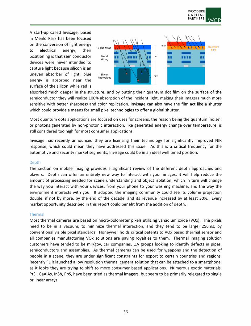
36
A start‐up called Invisage, based
in Menlo Park has been focused
on the conversion of light energy
to electrical energy, their
positioning is that semiconductor
devices were never intended to
capture light because silicon is an
uneven absorber of light, blue
energy is absorbed near the
surface of the silicon while red is
absorbed much deeper in the structure, and by putting their quantum dot film on the surface of the
semiconductor they will realize 100% absorption of the incident light, making their imagers much more
sensitive with better sharpness and color replication. Invisage can also have the film act like a shutter
which could provide a means for small pixel technologies to offer a global shutter.
Most quantum dots applications are focused on uses for screens, the reason being the quantum ‘noise’,
or photons generated by non‐photonic interaction, like generated energy change over temperature, is
still considered too high for most consumer applications.
Invisage has recently announced they are licensing their technology for significantly improved NIR
response, which could mean they have addressed this issue. As this is a critical frequency for the
automotive and security market segments, Invisage could be in an ideal well timed position.
Depth
The section on mobile imaging provides a significant review of the different depth approaches and
players. Depth can offer an entirely new way to interact with your images, it will help reduce the
amount of processing needed for scene understanding and object isolation, which in turn will change
the way you interact with your devices, from your phone to your washing machine, and the way the
environment interacts with you. If adopted the imaging community could see its volume projection
double, if not by more, by the end of the decade, and its revenue increased by at least 30%. Every
market opportunity described in this report could benefit from the addition of depth.
Thermal
Most thermal cameras are based on micro‐bolometer pixels utilizing vanadium oxide (VOx). The pixels
need to be in a vacuum, to minimize thermal interaction, and they tend to be large, 25ums, by
conventional visible pixel standards. Honeywell holds critical patents to VOx based thermal sensor and
all companies manufacturing VOx solutions are paying royalties to them. Thermal imaging solution
customers have tended to be mil/gov, car companies, QA groups looking to identify defects in pipes,
semiconductors and assemblies. As thermal cameras can be used for weapons and the detection of
people in a scene, they are under significant constraints for export to certain countries and regions.
Recently FLIR launched a low resolution thermal camera solution that can be attached to a smartphone,
as it looks they are trying to shift to more consumer based applications. Numerous exotic materials,
PtSi, GaAlAs, InSb, PbS, have been tried as thermal imagers, but seem to be primarily relegated to single
or linear arrays.
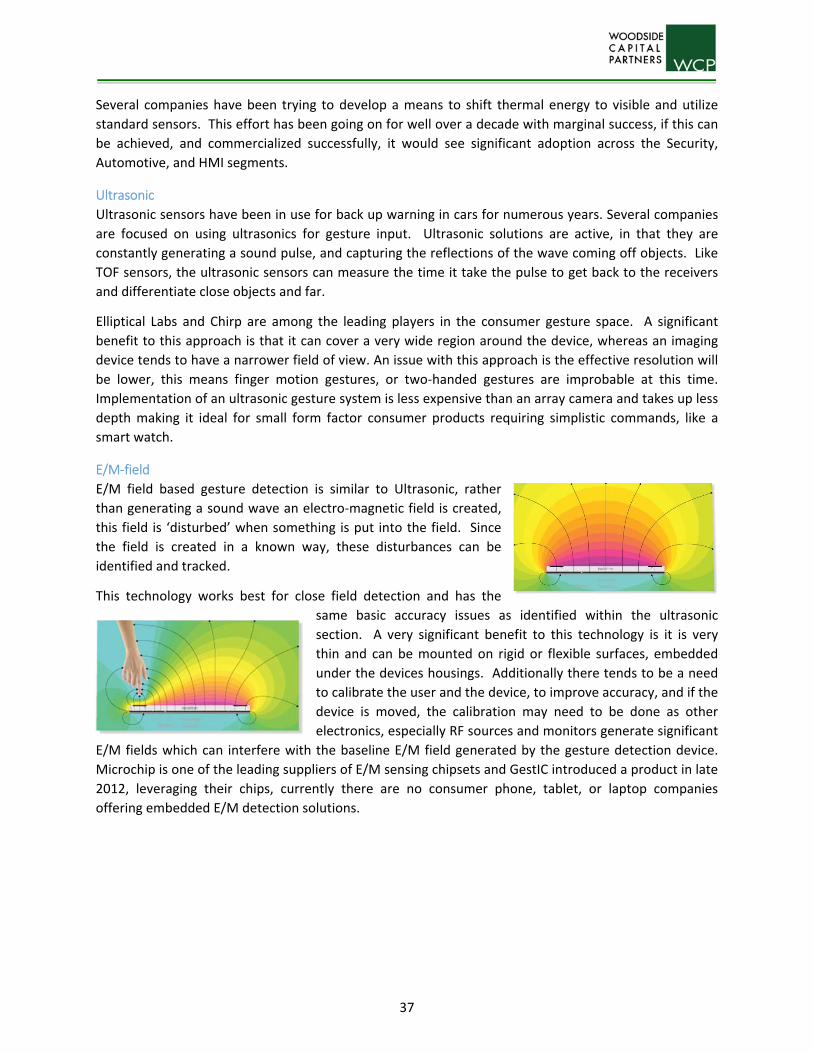
37
Several companies have been trying to develop a means to shift thermal energy to visible and utilize
standard sensors. This effort has been going on for well over a decade with marginal success, if this can
be achieved, and commercialized successfully, it would see significant adoption across the Security,
Automotive, and HMI segments.
Ultrasonic
Ultrasonic sensors have been in use for back up warning in cars for numerous years. Several companies
are focused on using ultrasonics for gesture input. Ultrasonic solutions are active, in that they are
constantly generating a sound pulse, and capturing the reflections of the wave coming off objects. Like
TOF sensors, the ultrasonic sensors can measure the time it take the pulse to get back to the receivers
and differentiate close objects and far.
Elliptical Labs and Chirp are among the leading players in the consumer gesture space. A significant
benefit to this approach is that it can cover a very wide region around the device, whereas an imaging
device tends to have a narrower field of view. An issue with this approach is the effective resolution will
be lower, this means finger motion gestures, or two‐handed gestures are improbable at this time.
Implementation of an ultrasonic gesture system is less expensive than an array camera and takes up less
depth making it ideal for small form factor consumer products requiring simplistic commands, like a
smart watch.
E/M‐field
E/M field based gesture detection is similar to Ultrasonic, rather
than generating a sound wave an electro‐magnetic field is created,
this field is ‘disturbed’ when something is put into the field. Since
the field is created in a known way, these disturbances can be
identified and tracked.
This technology works best for close field detection and has the
same basic accuracy issues as identified within the ultrasonic
section. A very significant benefit to this technology is it is very
thin and can be mounted on rigid or flexible surfaces, embedded
under the devices housings. Additionally there tends to be a need
to calibrate the user and the device, to improve accuracy, and if the
device is moved, the calibration may need to be done as other
electronics, especially RF sources and monitors generate significant
E/M fields which can interfere with the baseline E/M field generated by the gesture detection device.
Microchip is one of the leading suppliers of E/M sensing chipsets and GestIC introduced a product in late
2012, leveraging their chips, currently there are no consumer phone, tablet, or laptop companies
offering embedded E/M detection solutions.

38
Lens
Speed Trends
Until the iPhone 4S camera phone lenses were f#2.8. This lens
speed produces an airy disc (sharpest the lens can be focused to)
of about 3.7um. This means all of your 5Meg smartphones were
lens limited in resolution and actually were providing an effective
resolution on the order of 1.35 Meg, and your earlier 3Meg
cameras were less than 1Meg. The iPhone 4S offered a lens with
an f#2.4. This increased the amount of light getting to the sensor by 150%, thus improving the
performance of the camera, and reduced the airy disk size to 3.2um, increasing the effective resolution
of the 5Meg camera to 1.5Meg. The industry has followed Apple’s move and has shifted to f#2.4, it will
continue to pursue faster lenses. The HTC One had the first camera with an f#2.0 lens, the airy disc size
for this lens was 2.7um, this means this was the first cell phone camera whose resolution was not lens
limited since the 1Meg cameras.
Building faster lens small form factor cameras are non‐trivial. It
was reported that the 4S camera was 30% more expensive than
the iPhone 4. Traditionally it also created a thicker lens stack, this
is being gotten around by making thinner lenses, reducing the air
gap between the sensor and lens and changing the packaging and
housings for the sensor. However a more fundamental issue
related to lens speed is the faster the speed (lower the f# number)
the thinner the depth of field. From a photograph point of view
this means a slight movement of the camera towards or away
from the object after autofocus settles, could cause the region of interest in the scene to shift out of
focus. From a manufacturing point of view, this means the module alignment tolerances are much
tighter, as the speed of the lens increases to an f#2.0 it is expected that all modules will need to be built
utilizing active alignment.
Auto‐Focus AF actuators
The traditional AF actuator is based on voice coil technology. Voice coil is low cost and low power,
however it has a fundamental issue. The issue is the lens has no idea of its position relative to the depth
points in the scene. This means on power up or once it loses position it needs to scan every setting then
move back to the right position, if the actuator is designed for 17 steps this means on power up it needs
to move through the initial 17 steps then step back by each step until it gets to the right position. If you
are focusing on something close to the camera this could take all 34 steps, which translates to between
1‐2 secs before the camera is focused correctly. If you move your camera from a far distance shot to
capture something happening close to the camera it needs to repeat the process described above. One
of the top complaints from digital camera users is the time it takes to get from power up to first shot,
and shot to shot speed.
MEMs
MEMs based technology does not need to shift across all its steps and can move from one step to any
other step, this means it can hunt for best position through several different fast search algorithms

39
approaches, it is low power, and is starting to make penetration into Smartphones, Nokia, Google, and
Oppo have all announced cameras based on MEMs autofocus, this is significant as it is the first real
threat to the voice coil technology. MEMs had suffered for many years with not being able to survive a
drop test, this issue has been resolved and the industry is poised for a shift from voice coil to MEMs.
Since this technology can move so quickly it can take numerous images at numerous step points and
with processing can combine the sharp regions of each image to create and all‐in‐focus image. However,
just like the multi‐frame high dynamic range technique images captured over time opens the door for
motion artifacts. The speed of MEMs helps minimize this, but the problem can still exist. Tessera
recently announced it is shutting down its MEMs manufacturing group, Digital Optics Corp, DOC, to
instead focus on licensing the technology. With DOC now out, poLight is the huge winner in this race
and is well positioned for strong growth. Tessera can still license its technologies but as the majority of
the developers are no longer around to support the technologies implementation it looks more like they
need to wait for someone to infringe on their IP to realize any ROI on their investment.
poLight is the other player in this space and has modules
deployed in Nokia phones, and given the prerelease details
may also be in the Galaxy S5. poLight’s approach is to not
move any lenses instead they have a piezo on a glass
membrane with a polymer underneath. When a voltage is
applied the glass membrane is put under pressure and
bends which changes the optical power and allows
focusing. A significant benefit to the approach, is it only
needs to be powered when focusing, if the lens is designed
for far distance focus the piezo will not need to be
operated
Liquid Crystal
Liquid crystal technology takes advantage of the ability to
steer light through certain materials by creating an electric
field. This field causes the crystals to shift their position,
causing the light to refract at a steeper angle as it traverses
the material, the higher the field strength the more the
crystals shift. The material is placed in the lens path, around
the edge of this material a circuit laid out in a circular
manner. A voltage is applied to the circuit, and a field is
created, stronger near the circuit and falling off the farther
you get from the circuit. This means the light from the edge
is refracted at a higher angle than the light at the center,
which mimic what a lens does. By varying the voltage you vary the angle of refracted light, or the focal
point of the lens. This means, rather than moving lenses like voice coil and MEMs do to achieve AF this
solution is entirely solid state.
There are two fundamental problems with the technology. The first is the crystals absorb 5%‐10% of the
light transmitting through the material, and as camera phones are light starved, this is a serious problem
for adoption. The even more fundamental problem is the technology has not been able to extend the

40
field across a 1/3” optical format. Historically optical formats below 1/3” are viewed as the low end
segment and tend to be fixed focus based solutions, in essence they have a technology that had no place
to be utilized. A light may be visible in this long dark tunnel however, and that light may be coming from
selfies. The front facing camera is being used more and more for selfies, and resolutions being
considered are as high as 8Mpix, but the optical format would be ¼” or smaller. As selfies are closer
focus than typical, a fast solid state camera solution could be well positioned. The 2 primary players in
this technology are LensVector and eVision. To date neither company has been adopted into a camera
phone, Varioptic had a solution deployed in PC Cams several years ago, refocused their efforts to drive
to a mobile phone adoption.
Deformable
A liquid lens uses one or more fluids to create
an infinitely‐variable lens without any moving
parts by controlling the meniscus (the surface
of the liquid.)
Transmissive liquid lenses use two immiscible
fluids, each with a different refractive index,
to create variable‐focus lenses of high optical
quality as small as 10 µm (microns). The two
fluids, one an electrically conducting aqueous
solution and one a nonconducting oil, are contained in a short tube with transparent end caps. The
interior of the tube and one of the caps is coated with a hydrophobic material, which causes the
aqueous solution to form a hemispherical lens‐shaped mass at the opposite end of the tube. The shape
of the lens is adjusted by applying a dc voltage across the coating to decrease its water repellency in a
process called electrowetting. Electrowetting adjusts the liquid's surface tension, changing the radius of
curvature in the meniscus and thereby the focal length of the lens. Only 0.1 microjoules (µJ) are needed
for each change of focus. The lens is capable of seamless transition from convex (convergent) to concave
(divergent) lens shapes with switching times measured in milliseconds. In addition, the boundary
between the two fluids forms an extremely smooth and regular surface, making liquid lenses of quality
suitable space‐constrained high‐resolution applications like mobile cameras.
That being said, there have been issues, which have slowed the adoption of this technology, namely
temperature stability and vibration. Early samples of the materials were not temperature stable, and
had issues with vibration, especially as associated with hand jitter. The technology has evolved over the
last 10+ years and now claims to have resolved these issues. Cognex has rolled out a series of handheld
barcode reading products leveraging liquid lens technology. Varioptic is the last one standing for this
technology and seems to have shifted its focus from Mobile cameras to higher end and higher priced
applications, like the Cognex bar code reader. They currently list ophthalmology , medical, 2D barcode
and industrial lenses as their focus
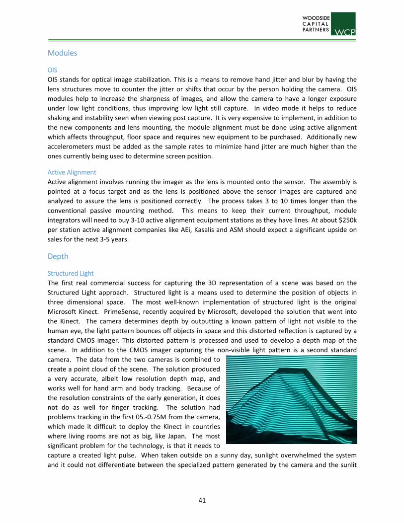
41
Modules
OIS
OIS stands for optical image stabilization. This is a means to remove hand jitter and blur by having the
lens structures move to counter the jitter or shifts that occur by the person holding the camera. OIS
modules help to increase the sharpness of images, and allow the camera to have a longer exposure
under low light conditions, thus improving low light still capture. In video mode it helps to reduce
shaking and instability seen when viewing post capture. It is very expensive to implement, in addition to
the new components and lens mounting, the module alignment must be done using active alignment
which affects throughput, floor space and requires new equipment to be purchased. Additionally new
accelerometers must be added as the sample rates to minimize hand jitter are much higher than the
ones currently being used to determine screen position.
Active Alignment
Active alignment involves running the imager as the lens is mounted onto the sensor. The assembly is
pointed at a focus target and as the lens is positioned above the sensor images are captured and
analyzed to assure the lens is positioned correctly. The process takes 3 to 10 times longer than the
conventional passive mounting method. This means to keep their current throughput, module
integrators will need to buy 3‐10 active alignment equipment stations as they have lines. At about $250k
per station active alignment companies like AEi, Kasalis and ASM should expect a significant upside on
sales for the next 3‐5 years.
Depth
Structured Light
The first real commercial success for capturing the 3D representation of a scene was based on the
Structured Light approach. Structured light is a means used to determine the position of objects in
three dimensional space. The most well‐known implementation of structured light is the original
Microsoft Kinect. PrimeSense, recently acquired by Microsoft, developed the solution that went into
the Kinect. The camera determines depth by outputting a known pattern of light not visible to the
human eye, the light pattern bounces off objects in space and this distorted reflection is captured by a
standard CMOS imager. This distorted pattern is processed and used to develop a depth map of the
scene. In addition to the CMOS imager capturing the non‐visible light pattern is a second standard
camera. The data from the two cameras is combined to
create a point cloud of the scene. The solution produced
a very accurate, albeit low resolution depth map, and
works well for hand arm and body tracking. Because of
the resolution constraints of the early generation, it does
not do as well for finger tracking. The solution had
problems tracking in the first 05.‐0.75M from the camera,
which made it difficult to deploy the Kinect in countries
where living rooms are not as big, like Japan. The most
significant problem for the technology, is that it needs to
capture a created light pulse. When taken outside on a sunny day, sunlight overwhelmed the system
and it could not differentiate between the specialized pattern generated by the camera and the sunlit

42
background. This system works quite well for indoor depth generation and mapping, and despite losing
the second generation Kinect socket, Primesense was seeing a broad adoption of their technology into
cameras designed to render real objects into a 3D representation of the object for printing by 3D
printers. The solution Microsoft and PrimeSense put together was a commercial success, Microsoft
opted for an alternate technology, Time of Flight for their second generation solution.
Time of Flight
Time of flight cameras are another active illumination solution to capture the depth of a scene. As it
generates a non‐visible light it also has the same problems the
structured light approach has when outside in sunlight. The time of
flight solution requires a specially designed image senor. Normal pixels
in an image sensor record the intensity of light that hits the pixel. A
time of flight camera records the phase of the light. The consumer
approach modulates the generated light with an RF carrier, then
measures the phase shift of the carrier at the pixel and translates that to the total distance traveled. It is
then a simple triangulation calculation to determine how much of the distance travelled was the return
from the object relative to the camera. There are several suppliers of chips for this technology, TI, PMD,
Infineon, Optix and Melexis are the leading suppliers.
Multi‐Camera
Lens Array
The lens array approach is similar to what Lytro does, they take an
existing camera design and add another lens element. This element
has a surface that has numerous small arrays which breaks up the
image into something that simulates a bugs eye view, these
different views of the scene are somewhat overlapping from lens to
lens, and this is utilized by the computational imaging processing
software to determine the depth of points in the scene, and the
software recombines the bugs eye view into a more traditional
human perceived view of the scene. The products that have been
released to date have 2 fundamental issues. The first is by adding an extra lens element the module
thickness is increased, for mobile applications module thickness is a critical parameter that the industry
is always trying to decrease. The more significant issue is the camera shows a very significant loss of
resolution relative to what resolution the camera had prior to adding the lens array. The image sensor
used in the initial Lytro camera had a resolution of 14Mpix, the resultant resolution of the image after
Lytro’s computational camera processing was more on the order of 1Mpix.
Sensor Array/Stereo
A sensor array approach is what companies like Pelican Imaging, Heptagon, Lynx Toshiba, and
CorePhotonics are pursuing. This approach is to put numerous camera modules together to provide
multiple views of the entire scene in higher resolution. The claims are that the data from several smaller
resolution cameras can be combined to produce a higher resolution final solution. Pelican’s initial
implementation had a 4x4 array of low resolution cameras with a total pixel count
above 10Mpix which when combined produced an image with an effective resolution

43
between 4Mpix‐5Mpix. This is in line with what imaging scientists had historically expected. Other
array camera developers are claiming no loss of resolution relative to the total number of pixels, as an
example they are claiming 4 5Mpix cameras combined produce a 20Mpix image. This seems
counterintuitive to what can be achieved from a physics perspective, but as these products approach
productization the validity will be established. Regardless of the final resolution the combination of
multiple cameras is based on getting more resolution from lower resolution imagers, lower resolution
imagers will have lower z heights which then opens up constraints for industrial designs. Toshiba claims
they have a solution where 2 5Mpix cameras produce a resultant 13Mpix image. Currently 5Mpix
camera modules are about 4mm thick, whereas 13Mpix cameras are 5.2‐6.0 mm thick. This is a
considerable reduction in height and if Toshiba claims can be realized this will completely change the
camera industry. An additional benefit from sensor array cameras is like lens array cameras they can
find the depth of points in a scene. This then provides a means to adapt the autofocus, if one exists,
faster, or to enable the user to change the focal point, lighting, or color effects post capture. It also is
claiming the ability to easily isolate objects in the scene. This then can improve imaging analytics from
skin tone enhancement to digital cosmetics on the consumer side, and presence detection and activity
monitoring on the commercial (security/automotive) side. One other approach is to use different lens
fields of view for different sensors, this then enables a means to achieve optical zoom performance in a
footprint small enough to fit in a cell phone and, as it is based on existing lens module technologies, can
also survive the standard drop and torture tests that phones undergo prior to release.
This technology has stirred up the traditional camera market in a way that hasn’t been seen since the
development of CMOS image sensors. There are numerous programs, implementations and
partnerships being developed by all of the major OEMs at this time and it is expected there will quite
few multi‐camera and array camera phones to follow the HTC One’s release.
Image Processing
Multispectral
Multispectral imaging is combining visible imaging with a non‐visible frequency, typically NIR or LWIR.
NIR energy frequencies can be captured by a standard visible pixel and typical cameras add a NIR block
filter to the optical path so the NIR energy does not affect image quality. A benefit of utilizing NIR
wavelengths for imaging is that this is light which is not seen by a person. With a NIR light source you
can capture images for a scene that looks like it is in the dark to a person, but in fact is very well lit from
an image sensor perspective. This is ideal for indoor gesture and gaming, as you want to make sure you
have enough light to capture a scene, but don’t want the light source to interfere with a person viewing
a screen. Automotive and Security/surveillance markets want both visible and NIR imagery, the benefit
here is to be able to capture a scene having a bright visible light source. The problem has been
traditional blue, green, and red color filters used for image sensors also pass NIR energy, this will then
affect the energy captured for each pixel, as the processing algorithms have no way to know how much
of the energy is NIR and how much is blue it treats all of the energy as blue which then affects color
fidelity. Camera manufacturers who needed both color and NIR performance would need to physically
move the filter out of the lens path when putting the camera into NIR mode. There had not been a filter
that could pass only a particular color and simultaneously block NIR, in fact there hadn’t been a filter to
block NIR that could be laid down on a pixel, until potentially recently. Several of the color filter
manufacturers are claiming to have developed materials that can block IR and be laid down during the

44
silicon manufacturing process. These materials are currently under testing and may be ready later in
2014. Additionally techniques are being developed to absorb NIR energy in a non‐electrically connected
region of a pixel. The benefit to either approach being developed is then RGB‐NIR color patterns can be
developed for image sensors. This would require specialized interpolation and processing, but would
give rise to single sensor solutions that could be used as your embedded laptop or front facing camera
as well as your gesture recognition sensor, or remove the need for security cameras to have to add a
mechanism to move the NIR filter out of the way. Fujifilm, Toppan, and JDSU are some of the major filter
material companies.
This technology can also potentially offer a significant benefit to consumer cameras. Low light imaging
has always been a problem for cameras, adding a standard white light flash is annoying to the people in
the scene as well as anyone in the area. By utilizing an NIR flash under low light conditions, the NIR
sensitive pixel can be used to support the luminance processing of the scene, this would improve edge
representation and overall light level of the resultant picture. The color filtered pixels would not ‘see’
the flash and so would have to boost the gain significantly, which adds the noise you are used to seeing
in low light images. As the NIR pixels had a flash source they will not have this increase in noise from
higher gain settings. The color and NIR versions of the scene can then be analyzed for disparities in
texture in the scene. When both versions see texture the algorithms know to not heavily filter that
region of the scene. When the color version shows high texture (noise) and the NIR version does not,
the algorithms know to apply a heavy low pass filter to reduce the noise. As the NIR image is also
supporting the edge detail this heavy filtering can be applied with minimal impact on the sharpness of
the scene. Early analysis shows this technique can help to improve the overall cameras low light
performance by 2 f‐stops, 4X, over a standard Bayer filter. This could prove to be a means to shift the
1.1um or <1um pixel performance to what was being seen with the 1.75um pixel with only a minor
change in the lens NIR filter.
45
Private Companies
Components
Invisage
InVisage Inc. has raised approximately $47.5M and is a 45 person company
based in Menlo Park CA and was founded in October 2005, leveraging research
and technology from the University of Toronto. It is focused on developing
Quantum Dot technology for image sensors. This is a unique position as the rest
of the quantum dot companies have been focused on displays. This is also a much more difficult
proposition as image sensors are less lenient to noise and non‐uniformity. They raised more than
$20Million in Feb 2013 to support the manufacturing of image sensors with the quantum dot film, and
have been quoted as expecting product to hit the market later this year. More recently a press release
went out saying they are ready to start licensing their technology for improvements in NIR sensitivity.
poLight
poLight has raised over $40M, is headquartered in Norway and claims to have
developed the fastest autofocus actuated lenses with absolutely no moving parts. Its
patented proprietary technology enables the production of wafer scale active optical
components based on deformable polymers. poLight's technology fits well into mobile
phone camera form factors, works with solder reflowable manufacturing techniques and claims to have
minimal impact on image quality. It has fast response time and is rumored to be in Nokia’s all‐in‐focus
camera phones.
LensVector
LensVector had raised more than $50M, their latest funding, $12.4M came in Dec 2013.
Their approach transforms a liquid crystal cell into an electronically controlled variable
focus lens. Since there are no moving parts, it is inherently rugged and reliable. The
technology moves molecules, not mechanisms, at a fraction of the size and power required for legacy
mechanical systems. Early revisions of the technology had difficulty working with lenses larger than ¼”
which is lower than the sweet spot for camera phones, and there was a reduction in light throughput by
10%. Lensvector was designed into a Spracht aftermarket PC cam in 2011, and claims it will be ready for
high volume production in 2013
Aptina
Aptina is a privately held company that includes Micron, TPG and Riverwood
Capital. Aptina is one of the world's leading imaging‐solutions company;
providing CMOS image sensors, and image processors. They saw considerable
success as the sole sensor provider for the Motorola Razer flip phones and the very successful Nokia
N95. They have expanded into HDI, Security, Automotive, and DSLR. They missed the mobile market
technology shift to backside imagers, and have had a hard time getting back into the mobile market.
The most successful HDI program was providing the imagers for the first gen Kinect gesture camera, but

46
with Microsoft shifting to time of flight sensors, that opportunity is fading, they may be able to leverage
the Apple acquisition of Primesense (the creator of the Kinect camera) to win future Apple sockets.
Apple has acquired a large number of Aptina employees to form the basis of the Apple image sensor
group. They are seeing success in automotive and security, but these are considerably smaller markets
than mobile phones and so in the future may have problems negotiating wafer price reductions as
Omnivision, Sony and Samsung put more focus on these expanding markets.
Movidius
Movidius raised over $55M including $16M in a series D round July of 2013.
They are developing a massively parallel DSP chip due to sample Q2 2014. They
have positioned themselves as the general purpose processing chip powerful
enough to support the new computational camera processing chip, while
simultaneously general purpose enough to be agnostic to all of the different techniques being
implemented. They are part of Googles Project Tango, and multi‐camera cell phone platform that
supports depth and gesture processing. They find themselves in a very opportunistic position as the
current mobile apps processors are having a hard time supporting the processing requirements of most
first generation arraycam implementations, and so many of the arraycam software developers are
porting their software to the Movidius platform as an interim solution waiting for the apps processing
companies to catchup with the potential market shift.
Movidius is a venture‐backed company with investors including: AIB Seed Capital Fund, Atlantic Bridge,
Capital‐E, DFJ Esprit and Robert Bosch Venture Capital.
GeoSemi
GEO’s video processing technology was originally designed by Silicon Optix. In
2004 Silicon Optix acquired Teranex Inc which was an early partner in creating
the Realta chip. The core of the chip is based on a massively parallel SIMD
(Single Instruction Multiple Data) architecture. The core consists of 3072
processing elements (PEs) arranged in a 2‐D grid. During processing, each PE handles computations for a
single pixel of the input video data. The high degree of parallelism, enables the chip to achieve high
computational throughputs for video and image processing tasks. This high level of performance is
attained within a relatively small area of the Realta chip and dramatically outperforms GPUs. The
company is seeing success in markets that require geometric correction of a scene, such as wide field of
view cameras, and multi‐camera systems. These markets include Security, and Automotive
Metaio
Founded in 2003 in Munich, Germany by current CEO, Thomas Alt and current
CTO, Peter Meier, and was created from an initial project with Volkswagen and
later receiving a German grant with which the founders bootstrapped their enterprise.
In 2005 Metaio released the first end‐consumer Augmented Reality application called KPS Click &
Design, allowing users to place virtual furniture into an image. Metaio then released their Unifeye
Platform offering third parties the opportunity to create commercial AR solutions.
In 2006 Metaio released the first browser plug‐in for web‐based AR applications and shortly thereafter,
launched the first fully integrated AR app for mobile devices and the first print/web campaign followed

47
by the release of the mobile AR browser junaio. In 2011, Metaio won the ISMAR Tracking Competition
for the world's first mobile 3‐D tracking solution.
Kalray
MPPA MANYCORE relies on KALRAY’s proprietary core technology resulting of
more than 20 years of intensive research in the area of parallel processing.
KALRAY’s core is a 32‐bit Very Long Instruction Word (VLIW) processor running at
chip frequency. The Two ALU operate either independently in SIMD mode, executing up to four 16‐bit
operations in parallel, or in paired mode, performing 64‐bit arithmetic operations. Specialized
instructions enable efficient byte swapping and bit shuffling, such as needed in arraycam and object
tracking operations.
Apical
Apical is a UK based company focused on image enhancement founded in 1999. Apical’s
core expertise is in modelling how the eye adapts to different conditions, and they
leverage this to improve the perceived dynamic range and color fidelity of pictures. Apical
develops advanced image processing technology for a wide variety of applications. Their
processing is found in most consumer cameras. Their products range from discrete
imaging modules to complete camera and display subsystems. Their solutions are based on IP cores for
licensing or embedded firmware.
General Vision
General Vision is a small privately funded company based in Petaluma CA.
They have developed several products based on a massively parallel and
extensible neuromorphic pattern training and recognition technology.
CogniSight is the product focused on vision, it is a unique image learning and recognition engine which is
trainable and can deliver high speed recognition of objects and scenes with applications in machine
vision, video surveillance, predictive maintenance, video analytics and potentially computational
cameras. A key feature of CogniSight is its ability to match a pattern extracted from pixel data against a
massive amount of patterns within micro‐seconds. Secondly, a CogniSight engine can build
autonomously a knowledge base describing objects by simply teaching iconic representations of these
objects, their parse codes, SIFT/SURF vectors and other relevant features. The resulting knowledge can
be saved for incremental learning and portability to other imaging systems. All these features are
possible thanks to the usage of banks of neuromorphic chip which can learn and recognize patterns in
real‐time.
System/SW
PointGrab
PointGrab is one of the early movers in advanced hand gesture recognition
solutions. Founded in 2008 and based out of Israel, their solution is software or
IP license based. Their initial focus was on utilizing the existing front facing
camera, so worked without any depth cues. This means the commands were limited to hand motions
parallel to the surface of the phone and could not understand any commands that brought your hand
closer or farther from the camera. As the potential for depth detection hardware is making its way to
the mobile camera market PointGrab is adapting its algorithm’s. PointGrab’s software solution enables
48
TVs, PCs, tablets, smartphones and home appliances to be operated by a natural user interface using
hand shapes and movements.
PointGrab claims their proprietary Hybrid Action Recognition technology enables a device to better
anticipate, understand and analyze a user’s body language. The system can detect and analyze complex
situations of shapes and motion as well as differentiate gestures from ‘look‐alike’ gestures to make the
whole experience more reliable, accurate and effective. PointGrab’s advanced software can be
integrated as an end‐to‐end solution or as SDK, and is available on Linux, Android, Windows, iOS, and OS
X platforms
Eyesight
eyeSight is another early mover in the 2D gesture recognition space. Founded in
Israel in 2005, eyeSight’s gesture recognition technology allows users to interact with
their devices using simple and natural hand gestures. EyeSight’s Touch Free technology utilizes
advanced real‐time image processing and machine vision algorithms to track the user’s hand gestures
and convert them into commands. The technology is completely software based and they claim it is
independent of the underlying processor and camera hardware. eyeSight’s technology works with a
standard 2D camera, and is compatible with 3D stereoscopic sensors, and IR illumination. They claim
their technology can be easily integrated into various levels of the digital device: on the chipset level,
operating system, as part of the camera module, or simply integrated in application level.
Pelican
Pelican is a 45 person company based in Mountain View CA, focused on array
cameras. It was founded in 2008 they have raised $39M across 3 rounds. Pelican
Imaging is one of the first companies developing the Multi‐Camera Super‐
resolution approach and claims very strong IP position. The initial approach was to take an array of 16
imagers (4x4) on a single chip, each with less than 0.75Mpixel resolution, and the associated array of
lens elements are each on a single 4x4 substrate to produce a high resolution image. The projected
benefits are that the camera module height is on the order of 50% to 60% of a conventional mobile
phone module, a high resolution depth edge map can be developed that is perfectly aligned with the
color image, and the smaller arrays enable a simplified lens design with a single standard I/O interface.
Additionally there is considerable redundancy so the overall yield should be better than a conventional
imaging chip of the same size. This approach does have some issues, it requires a custom sensor and
lens assembly, and the back focal tolerances are much tighter than is currently being built for any non‐
optical image stabilized modules. This means it will likely necessitate active alignment which requires
special assembly equipment and takes longer to assemble. Processing of the image data is very
specialized and is not well suited for the traditional application processor architectures, (computational
camera) this means a special processor or custom ASIC will likely be needed, which adds more cost. The
initial positioning of the current Pelican solution was intended to be 8Mpixel, assembled units are
producing results more in line with a 5Mpixel conventional camera, as the current 5Mpixel cameras
available are based on a 1/5” optical format the overall height difference between the Pelican and an
equivalent resolution camera is approaching parity.
LeapMotion
LeapMotion offers a gesture recognition HW controller that can be plugged into a PC
to turn any device into a gesture recognition solution. It is also finding its way

49
embedded into PC keyboards. The HP Envy laptop and HP Leap keyboard both have LeapMotion’s
technology embedded within. The standalone device sits in front of the keyboard looking up rather than
on the display looking out. This means the region where your gestures are recognized is above the
device. This implementation has benefits and issues. The benefit is there is an area that recognizes your
gestures so it limits the system from misunderstanding general hand motion as commands, but it also
means your hands need to be close to the keyboard which somewhat limits its benefit as you can just as
easily access the keyboard or mouse.
Founded in 2010 as OcuSpec, the company raised a $1.3M seed financing round in June 2011 with
investments from venture capital firms Andreessen Horowitz and Founders Fund, SOS ventures as well
as several angel investors. In May 2012, Leap Motion announced a $12.75M Series A funding round led
by Highland Capital Partners. In January 2013, Leap Motion announced a further series B round of
funding for $30M. After operating in quiet since 2010, Leap Motion publicly announced its first product,
originally called The Leap, on May 21, 2012. The device started full‐scale shipping in July 2013.
GestureTek
Founded in 1986 GestureTek develops and licenses gesture recognition
software based on computer vision techniques. GestPoint technology is a
camera‐enabled video tracking software system that translates hand and body movement into
computer control, similar to PointGrab and eyeSight. The system enables users to navigate and control
interactive multi‐media and menu‐based content, engage in virtual reality game play, experience
immersion in an augmented reality environment or interact with a consumer device (such as television,
mobile phone or set top box) without using touch‐based peripherals. GestureTek’s gesture interface
applications include multi‐touch and 3D camera tracking. A GestureTek multi‐touch table with object
recognition is found at the New York City Visitors Center, and Melbourne’s Eureka Tower. GestureTek’s
3D tracking technology is used in a 3D television prototype from Hitachi and various digital signage and
display solutions based on 3D interaction. Qualcomm acquired some of GestureTek’s IP specifically
focused on mobile HDI, while GestureTek held on to assets associated with its public display and digital
signage business.
EyeTech
Founded in 1996, EyeTech Digital Systems designs, develops and sells eye tracking
hardware and software for the disability, consumer research, interactive display and
ergonomic markets. EyeTech has been focused on the mobility challenged,
paraplegic’s, quadriplegic’s, or other disorders that minimize fine muscle movements to control a
mouse. The approach for eye tracking is similar between the numerous eye tracking solutions. An
imager with a NIR notch optical filter is positioned mechanically between 2 NIR LED sources whose
output frequency fall within the NIR notch optical filter. The imager ‘sees’ the two points reflecting off
the users eye (one point from each source) and based on the position of the two points can determine
where the eye is looking. This approach is old enough that the base IP is no longer able to be patent
protected. The barrier to entry is low
Chirp
Chirp was founded in late 2013 by a group of research engineers at the UC
Berkeley to allow electronic devices to recognize hand gestures, similar to
Microsoft's Kinect—with a major difference. Instead of using light, the new

50
technology is based on sound waves. The group is currently forming a spinoff company to develop and
market the technology, called Chirp Microsystems (the technology itself is called simply Chirp).
Chirp’s founder claim that using light as a medium to support gesture recognition required bulky
equipment and would only work in optimal situations. That caused them to turn to studying sound as a
means of sending information instead. That in turn led to the development of two computer chips, one
is an ultrasound chip, the other is a chip that sends and receives electrical signals from the ultrasound
chip. A third component is a battery. The system works by generating sound wave pulses using a very
tiny array of sound transducers (speakers). The chip then listens to the pulses when they are bounced
back. Doing so allows the chip to calculate how far away something is, just like radar. The new
technology uses just a fraction of the power of light based systems, and it's small enough to be
embedded in even the smallest devices, such as smartwatches.
51
Public Companies/Divisions
Components
Omnivision
Omnivision Technologies (NASDAQ: OVTI) was founded in 1995 as one of the earliest
CMOS imaging companies. They have expanded into wafer level module
manufacturing, and LCOS display products. They are focused on a broad number of
consumer and commercial applications, including mobile phones, notebooks, netbooks
and webcams, security and surveillance, entertainment, digital still and video cameras,
automotive and medical imaging systems and are typically first or second in terms of market share in
each of these segments. It had been reported that until the last version of the iPhone Omnivision was
the sole sensor supplier to Apple’s phones. Omnivision was the first company to commercialize
backside image sensor, and saw considerable success as the market shifted from the frontside to
backside based technology. Most recently it has been revealed that they are the sensors in the new HTC
One multi‐camera phone and Googles project Tango, both early implementations of the array camera
market shift detailed earlier. Currently Omnivision has approximately 30% of the worldwide market
share for CMOS imaging sensors with about 2000 employees worldwide. For fiscal 2013, Omnivision
reported revenues of $1,407.9 million. Omnivision is a fabless semiconductor company with access to
several fabs. This could prove very beneficial if mobile phones shift to array cameras.
Sony
Sony entered the CMOS imaging space later than most competitors, but has quickly
established itself as the technology leader. This position is based on both focused early
development effort on developing product for backside imaging technology well
before the technology saw broad adoption and on committing about twice the design
and marketing resources than its competitors. Sony CMOS Image sensor group is one
of the three key business’s Sony is focusing on for its turn around. The other two divisions however are
not yet profitable, while the CMOS imaging group is. Sony’s CMOS imaging group has been focused on
the high end of the consumer segments, and is reported to have generated over $3B in sales for 2013.
They were in both the Samsung and Apple flagship phones, however it has been reported Samsung SLSI
has taken back the next Generation Samsung Phone. Sony has brought in more capacity through its
purchase of the Renesa's 12 inch fab. It would not be surprising to see Sony extend its focus from the
high end markets to segments that are less price elastic as it looks to fill the capacity of the new fab.
This should present price pressure on the rest of the industry, and put at risk any CMOS imager
companies that are not well financed and positioned.
Samsung SLSI
Samsung SLSI has seen considerable success over the last 7‐8 years. It is not
coincidental that this is also the same time that Samsung has seen success with its
smartphone products. Samsung’s CMOS imaging group has primarily been focused on
supporting the Samsung Mobile. They have had success at Nokia and HTC in the past
but ass the Mobile Group continues to dominate they must deal with the issue of other
potential customer leery about revealing a detailed roadmap, or about allocation prioritization.

52
Samsung Mobile recent announcement revealed the SLSI image sensor will have PDAF to support fast
autofocus, and the pixel has an isolation technology, deep trench isolation embedded in it to minimize
signal crosstalk between pixels. This is a critical technology for the next generation of pixels which
would <1.0um in size. Samsung, Sony and Omnivision take up the lion’s share of the CMOS imaging
mobile market with on the order of 75% of the market split between them
Intel
After ignoring the mobile market for numerous years Intel is now focusing on
developing product lines specifically targeted at the mobile market, it is several
generations into these mobile focused products but still has seen little adoption in
the main smartphone markets. Intel is starting to see some success in the tablet
market, and is leveraging its Trisistor technology as a means to supply processor with significantly lower
overall power consumption. Intel has adopted ARM based processor’s to ease shifting costs, but as
Apple is well aware of in their attempts to minimize their reliance on Samsung’s processor group, and
Intel was able to leverage in the OC space, switching from one processor to another is non‐trivial, and
fraught with risk.
Qualcomm
Qualcomm has seen considerable success as the world has transitioned to
smartphones, their market share is on the order of 80% of all non‐Apple
smartphones. They have numerous tiers of products to target from very high end
through very basic. Their image processing core is the basis of comparison for all other ISP’s and as it is
included as part of a baseline cost, minimizes the entry of 3rd party companies developing more
advanced image processing as adding this chip is a cost adder, not a cost shift exercise. Of course if the
market does undergo a shift to array cameras a standard Bayer ISP may prove to be problematic as few
of the array camera processing companies are utilizing Bayer filtered sensors. This will either drive
OEMs to implement a 3rd party chip or port the software to the processor. If Intel can show their
architecture is more power efficient for arraycam SW processing they might finally have the reason to
drive a switch. If Qualcomm can protect its share it should be able to leverage higher ASPs once it
embeds the ability for arraycam processing as the mid to high end mobile phone tiers would shift to the
new technology mandating they also adopt the higher end Qualcomm processors.
Mediatek
Mediatek has seen considerable success as a low priced smartphone processor for
China. Their technology and capabilities lag Qualcomm, but their price is much lower
and they are a significant threat to Qualcomm’s low end business. Mediatek’s ISP is
less powerful and capable than Qualcomm’s and if the market does shift to arraycams computational
cameras their expansion into the mid end smartphone market will be delayed. If the industry continues
on a more traditional evolution it would be expected that Mediatek should represent an immediate
threat to not only Qualcomm’s low end business, but their mid end business as well.
nVidia
nVidia has seen considerable success as a graphic processing chip to the PC industry and
had made significant inroads into the tablet business. Recently, however they are getting
pressure from Intel in the tablet space and this coupled with the continuing erosion of
53
the PC space could put significant pressure on future products. nVidia has been at the lead of the
computational camera technology and has announced processors designed to specifically support
arraycam and other depth based processing approaches. The problem has been the limited resource
the companies developing computational camera solutions have mean they have to pick a single
platform and that means picking Qualcomm as this is the solution that has the highest probability of
being used by their mobile phone OEMs.
Microchip
Microchip Technology Inc., a leading provider of microcontroller, mixed‐signal, analog and Flash‐IP solutions have developed what they are calling the world’s first single‐chip 3D gesture/free space position tracking solution. This is based on
E/M technology, and is currently commercially available with a reference system, consisting of the detection module and one example reference electrode. The GestIC® Technology enabled with the MGC3130 serves a wide range of applications in the computing (e.g., laptops, keyboards, input devices); lighting (e.g., lighting switches and controls); consumer‐electronic (e.g., audio docks, printers and copiers); and automotive markets (e.g., automotive interior controls), among others.
M&A Activity
# Date Acquiror Target
Transaction
Value ($M)
TV/Revenue
Multiple Target Business Description
1) 04/03/14 ON Semiconductor True Sense Imaging, Inc. $92.0 1.2x Truesense Imaging, Inc. is a provider of high‐performance image sensor devices addressing a wide range of industrial end‐
markets.
2) 03/26/14 Shenzhen ONAfilm Tech. Co., Ltd. DigitalOptics Corporation, Certain
Patents and Equipment Assets
$50.0 NA DigitalOptics Corporation, Certain Patents and Equipment Assets comprises patent license agreement for MEMS and camera
module technology, as well as a license agreement of certain software features of Tessera's FotoNation business.
3) 02/18/14 GSI Group Corporation JADAK Technologies, Inc. 93.3 NA JADAK Technologies, Inc. provides data collection and machine vision technologies to OEM medical device manufacturers.
4) 01/16/14 DVM Technology Bhd Design Dept Sdn Bhd NA NA Design Dept Sdn Bhd operates as architectural and 3D interior design and image consultants.
5) 01/08/14 Globus Medical, Inc. Excelsius Surgical, L.L.C. NA NA Excelsius Surgical, L.L.C. operates as a medical device company that develops surgical robotic guidance technologies
integrated to digital 3D imaging for the spine, brain, and musculoskeletal markets.
6) 12/03/13 TA Associates Management, L.P. CMOSIS nv NA NA CMOSIS nv develops, produces, and supplies customized CMOS image sensors.
7) 11/24/13 Apple Inc. PrimeSense Ltd. NA NA PrimeSense Ltd. develops 3D machine vision technologies for digital devices.
8) 10/25/13 E*TRADE Korea Co., Ltd. Vieworks Co. Ltd. 1.9 4.1 Vieworks Co., Ltd. manufactures camera systems, as well as digital imaging systems for radiography, digital fluoroscopy,
and angiography systems.
9) 10/02/13 Google Inc. Flutter, Inc. 40.0 NA Flutter, Inc. develops develops gesture recognition software that enables other user applications run by hand gestures.
10) 09/26/13 Nintendo Co. Ltd. PUX Corporation 0.4 0.1 PUX Corporation is engaged in the planning, design, and development of audio and video processing, voice recognition, and
image recognition software.
11) 08/12/13 FLIR Systems, Inc. DigitalOptics Corporation East,
Certain MicroNAOptics Business
Assets in Charlotte
14.9 NA Tessera Technologies Inc., Micro‐Optics Business Based in Charlotte, North Carolina produces and markets diffractive
optical elements, refractive optical elements, and integrated micro‐optic sub‐assemblies.
12) 07/16/13 Intel Corporation Omek Interactive, Ltd. 40.0 NA Omek Interactive, Ltd. designs, develops, and delivers gesture recognition and body tracking software solutions for
customers to add gesture‐based interfaces to their products.
13) 07/15/13 Digital Audio Corporation, Inc. Salient Stills, Inc. NA NA Salient Stills, Inc. provides video forensics and video image enhancement software solutions.
14) 07/10/13 DFJ Esprit LLP; Dublin Business
Innovation Centre, Investment Arm;
Enterprise Equity (Irl) Limited;
Western Investment Fund; Atlantic
Bridge; CapitalNAE NV; Robert
Bosch Venture Capital GmbH
Movidius Ltd. 16.0 NA Movidius Ltd. operates as a computational image‐processor chip and software company.
15) 07/02/13 Outerwall Inc. ecoATM, Inc. 262.9 NA ecoATM, Inc. builds automated self‐serve kiosks that use machine vision, electronic diagnostics, and artificial intelligence to
evaluate and buy‐back used electronics.
54
M&A Activity (continued)
# Date Acquiror Target
Transaction
Value ($M)
TV/Revenue
Multiple Target Business Description
16) 06/21/13 Saints Capital Merisel Inc. 0.4 0.5 Merisel Inc. supplies visual communication solutions.
17) 05/01/13 LMI Technologies Inc. 3D3 Solutions Inc. NA NA 3D3 Solutions Inc. develops 3D scanning and visualization technologies.
18) 04/08/13 Massive Dynamics, Inc. RealView Corporation 4.8 NA Real‐View Corporation develops and delivers scanners for capturing images in 3D.
19) 01/02/13 Manufacturing Integration
Technology Ltd.
Generic Power Pte Ltd. 0.5 NA Generic Power Pte Ltd. develops and sells machine vision systems for the semiconductor and other engineering industries.
20) 11/29/12 Carl Zeiss Industrial Metrology LLC Carl Zeiss Machine Vision GmbH &
Co KG
NA NA Carl Zeiss Machine Vision GmbH & Co KG develops machine vision systems.
21) 10/02/12 Motorola Mobility Holdings, Inc. Viewdle, Inc. 45.0 NA Viewdle, Inc. operates as a mobile‐focused computer vision company that enables the creation of new user experiences in
mobile gaming, social networking, social media, advertising, and marketing.
22) 09/18/12 Canon Europa N.V. Image Recognition Integrated
Systems Group S.A.
88.4 0.8 Image Recognition Integrated Systems Group sa, together with its subsidiaries, develops and sells intelligent document
recognition technologies and software packages to private and professional users worldwide.
23) 09/13/12 Sony Electronics, Inc. Pixim, Inc. NA NA Pixim, Inc. provides digital imaging systems that allow camera developers to design and build cameras.
24) 08/17/12 General Dynamics Broadband, Inc. Open Kernel Labs, Inc. NA NA Open Kernel Labs, Inc. provides systems software and virtualization technology for embedded systems.
25) 06/18/12 Facebook, Inc. Face.com 60.0 NA Face.com operates a technology platform with facial recognition software for photo sharing. It helps to tag, share, and find
users' and their friends' untagged photos.
26) 06/14/12 Nokia Scalado NA NA Scalado AB provides imaging technologies, applications, and engineering services for the camera phone industry
27) 04/26/12 JAI A/S TVI Vision Oy NA NA TVI Vision Oy manufactures color line scan cameras for industrial machine vision applications.
28) 04/17/12 Intel Korea Ltd. Olaworks, Inc. 31.0 NA Olaworks, Inc., a computer vision technology company, engages in the research and development of image recognition
solutions for smart devices.
29) 03/08/12 Microchip Technology Inc. IDENT Technology AG 39.8 NA IDENT Technology AG engages in the field of data transmission in capacitive near‐field and gesture‐supported man‐machine
control and markets its know‐how via licensing.
30) 03/02/12 Tessera North America, Inc. Vista Point Technologies, Inc.,
Zhuhai Camera Module Business
40.0 NA Vista Point Technologies, Inc., Zhuhai Camera Module Business engages in manufacturing of camera modules.
55
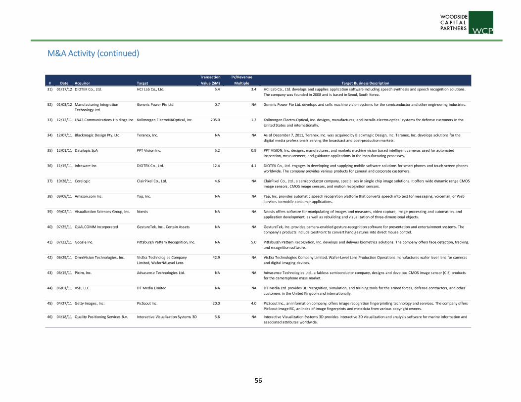
1
M&A Activity (continued)
# Date Acquiror Target
Transaction
Value ($M)
TV/Revenue
Multiple Target Business Description
31) 01/17/12 DIOTEK Co., Ltd. HCI Lab Co., Ltd. 5.4 3.4 HCI Lab Co., Ltd. develops and supplies application software including speech synthesis and speech recognition solutions.
The company was founded in 2008 and is based in Seoul, South Korea.
32) 01/03/12 Manufacturing Integration
Technology Ltd.
Generic Power Pte Ltd. 0.7 NA Generic Power Pte Ltd. develops and sells machine vision systems for the semiconductor and other engineering industries.
33) 12/12/11 LNA3 Communications Holdings Inc. Kollmorgen ElectroNAOptical, Inc. 205.0 1.2 Kollmorgen Electro‐Optical, Inc. designs, manufactures, and installs electro‐optical systems for defense customers in the
United States and internationally.
34) 12/07/11 Blackmagic Design Pty. Ltd. Teranex, Inc. NA NA As of December 7, 2011, Teranex, Inc. was acquired by Blackmagic Design, Inc. Teranex, Inc. develops solutions for the
digital media professionals serving the broadcast and post‐production markets.
35) 12/01/11 Datalogic SpA PPT Vision Inc. 5.2 0.9 PPT VISION, Inc. designs, manufactures, and markets machine vision based intelligent cameras used for automated
inspection, measurement, and guidance applications in the manufacturing processes.
36) 11/15/11 Infraware Inc. DIOTEK Co., Ltd. 12.4 4.1 DIOTEK Co., Ltd. engages in developing and supplying mobile software solutions for smart phones and touch screen phones
worldwide. The company provides various products for general and corporate customers.
37) 10/28/11 Corelogic ClairPixel Co., Ltd. 4.6 NA ClairPixel Co., Ltd., a semiconductor company, specializes in single chip image solutions. It offers wide dynamic range CMOS
image sensors, CMOS image sensors, and motion recognition sensors.
38) 09/08/11 Amazon.com Inc. Yap, Inc. NA NA Yap, Inc. provides automatic speech recognition platform that converts speech into text for messaging, voicemail, or Web
services to mobile consumer applications.
39) 09/02/11 Visualization Sciences Group, Inc. Noesis NA NA Neosis offers software for manipulating of images and measures, video capture, image processing and automation, and
application development, as well as rebuilding and visualization of three‐dimensional objects.
40) 07/25/11 QUALCOMM Incorporated GestureTek, Inc., Certain Assets NA NA GestureTek, Inc. provides camera‐enabled gesture‐recognition software for presentation and entertainment systems. The
company's products include GestPoint to convert hand gestures into direct mouse control.
41) 07/22/11 Google Inc. Pittsburgh Pattern Recognition, Inc. NA 5.0 Pittsburgh Pattern Recognition, Inc. develops and delivers biometrics solutions. The company offers face detection, tracking,
and recognition software.
42) 06/29/11 OmniVision Technologies, Inc. VisEra Technologies Company
Limited, WaferNALevel Lens
42.9 NA VisEra Technologies Company Limited, Wafer‐Level Lens Production Operations manufactures wafer level lens for cameras
and digital imaging devices.
43) 06/15/11 Pixim, Inc. Advasense Technologies Ltd. NA NA Advasense Technologies Ltd., a fabless semiconductor company, designs and develops CMOS image sensor (CIS) products
for the cameraphone mass market.
44) 06/01/11 VSD, LLC DT Media Limited NA NA DT Media Ltd. provides 3D recognition, simulation, and training tools for the armed forces, defense contractors, and other
customers in the United Kingdom and internationally.
45) 04/27/11 Getty Images, Inc. PicScout Inc. 20.0 4.0 PicScout Inc., an information company, offers image recognition fingerprinting technology and services. The company offers
PicScout ImageIRC, an index of image fingerprints and metadata from various copyright owners.
46) 04/18/11 Quality Positioning Services B.v. Interactive Visualization Systems 3D 3.6 NA Interactive Visualization Systems 3D provides interactive 3D visualization and analysis software for marine information and
associated attributes worldwide.
56

2
M&A Activity (continued)
# Date Acquiror Target
Transaction
Value ($M)
TV/Revenue
Multiple Target Business Description
47) 03/31/11 Eastman Park Micrographics, Inc. Eastman Kodak Co., Certain Assets
of Microfilm Products and
Equipment Business
NA NA Certain Assets of Microfilm Products and Equipment Business of Eastman Kodak Co. comprises microfilms products as well
as service and support agreement for microfilm equipment.
48) 03/30/11 Woodman Labs, Inc. CineForm Inc. NA NA CineForm Inc. develops and delivers compression based workflow solutions for films editing, effects, and mastering.
49) 02/21/11 CSR plc Zoran Corporation 456.6 0.6 Zoran Corporation provides digital solutions in the digital entertainment and imaging market worldwide.
50) 02/15/11 SMKNALink Electronics Corporation Movea, Inc. 5.0 NA Movea, Inc. provides wireless RF motion‐sensing controllers for the digital lifestyle markets. Its products include in‐air
mice/keyboards, in‐air remotes, Gyrotransport, portable air mouse, refurbished products, and accessories.
51) 02/14/11 Intel Corporation Silicon Hive BV NA NA Silicon Hive BV supplies semiconductor intellectual properties.
52) 01/27/11 ON Semiconductor Corp. Cypress Semiconductor Corp.,
CMOS Image Sensor Business Unit
34.1 NA Cypress Semiconductor Corp., CMOS Image Sensor Business Unit manufactures CMOS image sensors which are used in multi‐
megapixel digital photography and cinematography, machine vision, linear and two dimensional (2D) bar code imaging.
53) 01/18/11 Intermec, Inc. Vocollect, Inc. 197.0 1.7 Vocollect, Inc. provides voice solutions in industrial settings.
54) 01/11/11 Kopin Corporation Forth Dimension Displays Limited 18.0 3.0 Forth Dimension Displays Limited develops, manufactures, and supplies high‐resolution near‐to‐eye microdisplay.
55) 10/29/10 Microsoft Corporation Canesta, Inc. NA NA Canesta, Inc. provides electronic perception technology in the United States.
56) 09/02/10 Apple Inc. Polar Rose AB 29.0 NA Polar Rose AB provides online services.
57) 05/04/10 Tessera Technologies Inc. Tessera MEMS Technologies, Inc. 15.0 NA Tessera MEMS Technologies, Inc. develops and manufactures micro electro mechanical systems (MEMS) based camera
solutions for mobile imaging applications.
Mean $56.4 2.2x
Median 29.0 1.4
57

3
Appendix A: Private Company Additional Information

4

5

6

7

8

9

10

11

12

13

14

15

17

18

19
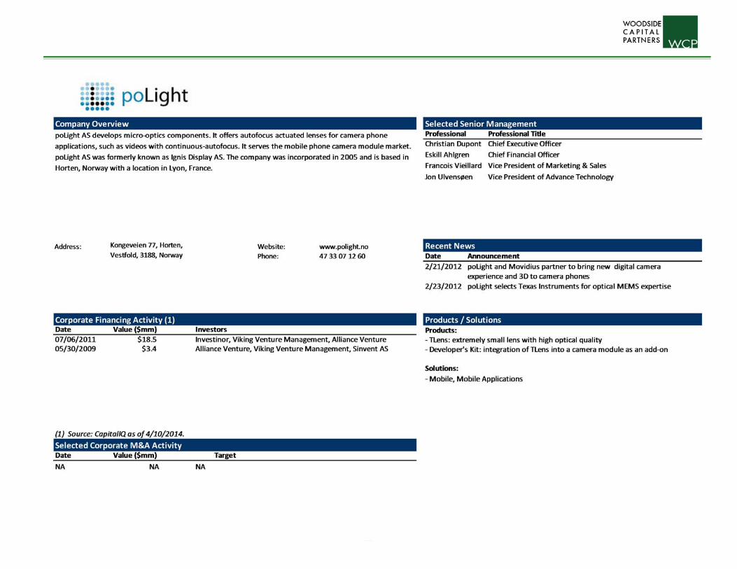
20

Appendix B: Public Company Additional Information
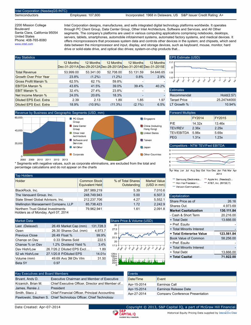
Date Created: Apr-07-2014 Copyright © 2013, S&P Capital IQ, a part of McGraw Hill Financial.Historical Equity Pricing Data supplied by
Intel Corporation (NasdaqGS:INTC)Semiconductors Employees: 107,600 Incorporated: 1968 in Delaware, US S&P Issuer Credit Rating: A+
2200 Mission CollegeBoulevardSanta Clara, California 95054United StatesPhone: 408-765-8080www.intel.com
Intel Corporation designs, manufactures, and sells integrated digital technology platforms worldwide. It operatesthrough PC Client Group, Data Center Group, Other Intel Architecture, Software and Services, and All Othersegments. The company’s platforms are used in various computing applications comprising notebooks, desktops,servers, tablets, smartphones, automobile infotainment systems, automated factory systems, and medical devices. Itoffers microprocessors that processes system data and controls other devices in the system; and chipsets, which senddata between the microprocessor and input, display, and storage devices, such as keyboard, mouse, monitor, harddrive or solid-state drive, and optical disc drives; system-on-chip products that...
Key Statistics12 Months
Dec-31-2011A12 Months
Dec-29-2012A12 Months
Dec-28-2013A12 Months
Dec-31-2014E12 Months
Dec-31-2015E
Total Revenue 53,999.00 53,341.00 52,708.00 53,131.59 54,646.65Growth Over Prior Year 23.8% (1.2%) (1.2%) 0.8% 2.9%Gross Profit Margin % 62.5% 62.1% 59.8% - -EBITDA Margin % 43.6% 41.5% 39.0% 39.4% 40.2%EBIT Margin % 32.4% 27.4% 23.8% - -Net Income Margin % 24.0% 20.6% 18.3% - -Diluted EPS Excl. ExtraItems
2.39 2.13 1.89 1.85 1.97Diluted EPS Excl. ExtraItems...
18.9% (10.9%) (11.3%) (2.1%) 6.5%
Revenue by Business and Geographic Segments (USD, mm)
* Segments with negative values, such as corporate eliminations, are excluded from the total andpercentage calculations and do not appear on the charts
Top HoldersHolder Common Stock
Equivalent Held% of Total Shares
OutstandingMarket Value(USD in mm)
BlackRock, Inc. 267,989,219 5.39 7,010.6The Vanguard Group, Inc. 248,749,943 5.00 6,507.3State Street Global Advisors, Inc. 212,237,706 4.27 5,552.1Wellington Management Company, LLP 85,738,423 1.72 2,242.9Northern Trust Global Investments 79,962,941 1.61 2,091.8Holders as of Monday, April 07, 2014
Market DataLast (Delayed) 26.49 Market Cap (mm) 131,728.3Open 26.30 Shares Out. (mm) 4,973.7Previous Close 26.49 Float % 99.9%Change on Day 0.33 Shares Sold
Short...222.5
Change % on Day 1.2% Dividend Yield % 3.4%Day High/Low 26.7/26.2 Diluted EPS Excl.... 1.8952 wk High/Low 27.1/20.8 P/Diluted EPS
Before...14.01x
Volume (mm) 49.69 Avg 3M Dly Vlm(mm)
31.50Beta 5Y 0.97
Share Price & Volume (USD)
EPS Estimate (USD)
EstimatesRecommendation Hold(2.57)Target Price 25.24744000LT Growth % 10.94%
Forward MultiplesFY2014 FY2015
P/E 14.32x 13.46xTEV/REV 2.36x 2.29xTEV/EBITDA 5.98x 5.69xPEG 1.31x 1.23x
Competitors - NTM TEV/Fwd EBITDA
CapitalizationShare Price as ofApr-04-2014
26.16Shares Out. 4,973.69Market Capitalization 130,111.84- Cash & Short TermInvestments
20,216.00+ Total Debt 13,666.00+ Pref. Equity -+ Total Minority Interest -= Total Enterprise Value(TEV)
123,561.84Book Value of CommonEquity
58,256.00+ Pref. Equity -+ Total Minority Interest -+ Total Debt 13,666.00= Total Capital 71,922.00
Key Executives and Board MembersBryant, Andy D. Executive Chairman and Member of Executive
CommitteeKrzanich, Brian M. Chief Executive Officer, Director and Member of...James, Renée J. PresidentSmith, Stacy J. Chief Financial Officer, Principal Accounting
Officer,...Pawlowski, Stephen S. Chief Technology Officer, Chief TechnologyOfficer for...
EventsDate/Time Event
Apr-15-2014 Earnings CallApr-15-2014 Earnings Release DateApr-27-2014 Company Conference Presentation

Date Created: Apr-07-2014 Copyright © 2013, S&P Capital IQ, a part of McGraw Hill Financial.Historical Equity Pricing Data supplied by
MediaTek Inc. (TSEC:2454)Semiconductors Employees: 6,999 Incorporated: 1997 in TA
No. 1, Dusing 1st RoadHsinchu Science ParkHsinchu 30078TaiwanPhone: 886 3 567 0766www.mediatek.com
MediaTek Inc., a fabless semiconductor company, is engaged in the research, development, production, manufacture,and sale of various integrated circuits (ICs) in Taiwan, Asia, and Internationally. It provides multimedia ICs, computerperipherals oriented ICs, consumer-oriented ICs, and other application ICs. The company offers chipsets forsmartphones, tablets, and feature phones; and HDTV, 3D TV, and smart TV platforms that support video on demand,video calls, and a range of wireless network standards for access to content. It also provides home and portableplatforms with video and audio codec support, and proprietary technology to enhance picture quality; and read-onlyand rewritable DVD and Blu-ray technology for internal and external optical...
Key Statistics12 Months
Dec-31-2011A12 Months
Dec-31-2012A12 Months
Dec-31-2013A
Total Revenue 2,867.63 3,414.16 4,554.17Growth Over Prior Year (23.5%) 14.3% 37.1%Gross Profit Margin % 45.3% 41.4% 44.0%EBITDA Margin % 17.0% 16.0% 19.7%EBIT Margin % 14.2% 12.5% 18.6%Net Income Margin % 15.7% 15.7% 20.2%Diluted EPS Excl. ExtraItems
0.40 0.44 0.68Diluted EPS Excl. ExtraItems...
(56.2%) 4.4% 60.2%
Revenue by Business and Geographic Segments (USD, mm)
* Segments with negative values, such as corporate eliminations, are excluded from the total andpercentage calculations and do not appear on the charts
Market DataLast (Delayed) 15.28 Market Cap (mm) 23,826.7Open 15.38 Shares Out. (mm) 1,562.8Previous Close 15.25 Float % 86.8%Change on Day 0.03 Shares Sold
Short...-
Change % on Day 0.2% Dividend Yield % 2.0%Day High/Low 15.4/15.2 Diluted EPS Excl.... 0.6852 wk High/Low 15.92/9.99 P/Diluted EPS
Before...22.67x
Volume (mm) 1.52 Avg 3M Dly Vlm(mm)
6.58Beta 5Y 0.31
Share Price & Volume (USD)
Competitors - NTM TEV/Fwd EBITDA
CapitalizationShare Price as ofApr-03-2014
15.33Shares Out. 1,562.80Market Capitalization 23,958.52- Cash & Short TermInvestments
4,656.25+ Total Debt 972.44+ Pref. Equity -+ Total Minority Interest 1.28= Total Enterprise Value(TEV)
20,275.98Book Value of CommonEquity
6,537.75+ Pref. Equity -+ Total Minority Interest 1.28+ Total Debt 972.44= Total Capital 7,511.46
Key Executives and Board MembersTsai, Ming-Kai Chairman and Chief Executive OfficerCho, Jyh-Jer Vice ChairmanHsieh, Ching-Jiang President and DirectorKu, David Chief Financial Officer and Vice PresidentJou, Kevin Chief Technology Officer and Vice President
EventsDate/Time Event
Apr-08-2014 Sales/Trading Statement Release DateApr-15-2014 Estimated Earnings Release Date (CIQ Derived)May-06-2014 Conference
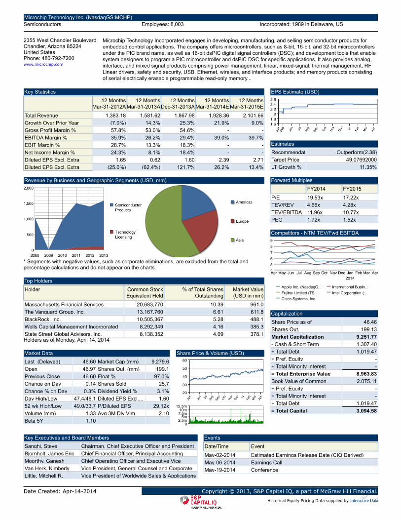
Date Created: Apr-14-2014 Copyright © 2013, S&P Capital IQ, a part of McGraw Hill Financial.Historical Equity Pricing Data supplied by
Microchip Technology Inc. (NasdaqGS:MCHP)Semiconductors Employees: 8,003 Incorporated: 1989 in Delaware, US
2355 West Chandler BoulevardChandler, Arizona 85224United StatesPhone: 480-792-7200www.microchip.com
Microchip Technology Incorporated engages in developing, manufacturing, and selling semiconductor products forembedded control applications. The company offers microcontrollers, such as 8-bit, 16-bit, and 32-bit microcontrollersunder the PIC brand name, as well as 16-bit dsPIC digital signal controllers (DSC); and development tools that enablesystem designers to program a PIC microcontroller and dsPIC DSC for specific applications. It also provides analog,interface, and mixed signal products comprising power management, linear, mixed-signal, thermal management, RFLinear drivers, safety and security, USB, Ethernet, wireless, and interface products; and memory products consistingof serial electrically erasable programmable read-only memory...
Key Statistics12 Months
Mar-31-2012A12 Months
Mar-31-2013A12 Months
Dec-31-2013A12 Months
Mar-31-2014E12 Months
Mar-31-2015E
Total Revenue 1,383.18 1,581.62 1,867.98 1,928.36 2,101.66Growth Over Prior Year (7.0%) 14.3% 25.3% 21.9% 9.0%Gross Profit Margin % 57.8% 53.0% 54.6% - -EBITDA Margin % 35.9% 26.2% 29.4% 39.0% 39.7%EBIT Margin % 28.7% 13.3% 18.3% - -Net Income Margin % 24.3% 8.1% 18.4% - -Diluted EPS Excl. ExtraItems
1.65 0.62 1.60 2.39 2.71Diluted EPS Excl. ExtraItems...
(25.0%) (62.4%) 121.7% 26.2% 13.4%
Revenue by Business and Geographic Segments (USD, mm)
* Segments with negative values, such as corporate eliminations, are excluded from the total andpercentage calculations and do not appear on the charts
Top HoldersHolder Common Stock
Equivalent Held% of Total Shares
OutstandingMarket Value(USD in mm)
Massachusetts Financial ServicesCompany
20,683,770 10.39 961.0The Vanguard Group, Inc. 13,167,760 6.61 611.8BlackRock, Inc. 10,505,367 5.28 488.1Wells Capital Management Incorporated 8,292,349 4.16 385.3State Street Global Advisors, Inc. 8,138,352 4.09 378.1Holders as of Monday, April 14, 2014
Market DataLast (Delayed) 46.60 Market Cap (mm) 9,279.6Open 46.97 Shares Out. (mm) 199.1Previous Close 46.60 Float % 97.0%Change on Day 0.14 Shares Sold
Short...25.7
Change % on Day 0.3% Dividend Yield % 3.1%Day High/Low 47.4/46.1 Diluted EPS Excl.... 1.6052 wk High/Low 49.0/33.7 P/Diluted EPS
Before...29.12x
Volume (mm) 1.33 Avg 3M Dly Vlm(mm)
2.10Beta 5Y 1.10
Share Price & Volume (USD)
EPS Estimate (USD)
EstimatesRecommendation Outperform(2.38)Target Price 49.07692000LT Growth % 11.35%
Forward MultiplesFY2014 FY2015
P/E 19.53x 17.22xTEV/REV 4.66x 4.28xTEV/EBITDA 11.96x 10.77xPEG 1.72x 1.52x
Competitors - NTM TEV/Fwd EBITDA
CapitalizationShare Price as ofApr-11-2014
46.46Shares Out. 199.13Market Capitalization 9,251.77- Cash & Short TermInvestments
1,307.40+ Total Debt 1,019.47+ Pref. Equity -+ Total Minority Interest -= Total Enterprise Value(TEV)
8,963.83Book Value of CommonEquity
2,075.11+ Pref. Equity -+ Total Minority Interest -+ Total Debt 1,019.47= Total Capital 3,094.58
Key Executives and Board MembersSanghi, Steve Chairman, Chief Executive Officer and PresidentBjornholt, James Eric Chief Financial Officer, Principal Accounting
Officer and...Moorthy, Ganesh Chief Operating Officer and Executive VicePresidentVan Herk, Kimberly Vice President, General Counsel and CorporateSecretaryLittle, Mitchell R. Vice President of Worldwide Sales & Applications
EventsDate/Time Event
May-02-2014 Estimated Earnings Release Date (CIQ Derived)May-06-2014 Earnings CallMay-19-2014 Conference
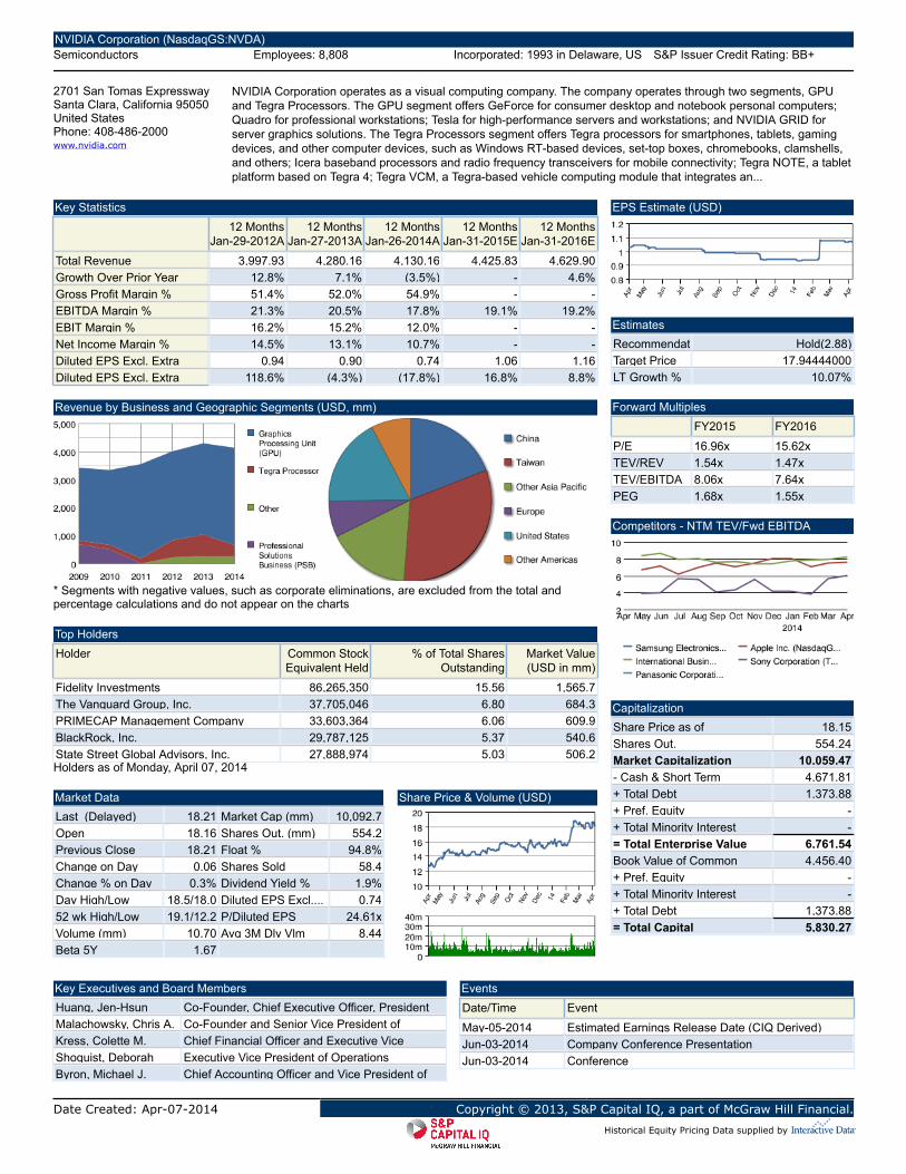
Date Created: Apr-07-2014 Copyright © 2013, S&P Capital IQ, a part of McGraw Hill Financial.Historical Equity Pricing Data supplied by
NVIDIA Corporation (NasdaqGS:NVDA)Semiconductors Employees: 8,808 Incorporated: 1993 in Delaware, US S&P Issuer Credit Rating: BB+
2701 San Tomas ExpresswaySanta Clara, California 95050United StatesPhone: 408-486-2000www.nvidia.com
NVIDIA Corporation operates as a visual computing company. The company operates through two segments, GPUand Tegra Processors. The GPU segment offers GeForce for consumer desktop and notebook personal computers;Quadro for professional workstations; Tesla for high-performance servers and workstations; and NVIDIA GRID forserver graphics solutions. The Tegra Processors segment offers Tegra processors for smartphones, tablets, gamingdevices, and other computer devices, such as Windows RT-based devices, set-top boxes, chromebooks, clamshells,and others; Icera baseband processors and radio frequency transceivers for mobile connectivity; Tegra NOTE, a tabletplatform based on Tegra 4; Tegra VCM, a Tegra-based vehicle computing module that integrates an...
Key Statistics12 Months
Jan-29-2012A12 Months
Jan-27-2013A12 Months
Jan-26-2014A12 Months
Jan-31-2015E12 Months
Jan-31-2016E
Total Revenue 3,997.93 4,280.16 4,130.16 4,425.83 4,629.90Growth Over Prior Year 12.8% 7.1% (3.5%) - 4.6%Gross Profit Margin % 51.4% 52.0% 54.9% - -EBITDA Margin % 21.3% 20.5% 17.8% 19.1% 19.2%EBIT Margin % 16.2% 15.2% 12.0% - -Net Income Margin % 14.5% 13.1% 10.7% - -Diluted EPS Excl. ExtraItems
0.94 0.90 0.74 1.06 1.16Diluted EPS Excl. ExtraItems...
118.6% (4.3%) (17.8%) 16.8% 8.8%
Revenue by Business and Geographic Segments (USD, mm)
* Segments with negative values, such as corporate eliminations, are excluded from the total andpercentage calculations and do not appear on the charts
Top HoldersHolder Common Stock
Equivalent Held% of Total Shares
OutstandingMarket Value(USD in mm)
Fidelity Investments 86,265,350 15.56 1,565.7The Vanguard Group, Inc. 37,705,046 6.80 684.3PRIMECAP Management Company 33,603,364 6.06 609.9BlackRock, Inc. 29,787,125 5.37 540.6State Street Global Advisors, Inc. 27,888,974 5.03 506.2Holders as of Monday, April 07, 2014
Market DataLast (Delayed) 18.21 Market Cap (mm) 10,092.7Open 18.16 Shares Out. (mm) 554.2Previous Close 18.21 Float % 94.8%Change on Day 0.06 Shares Sold
Short...58.4
Change % on Day 0.3% Dividend Yield % 1.9%Day High/Low 18.5/18.0 Diluted EPS Excl.... 0.7452 wk High/Low 19.1/12.2 P/Diluted EPS
Before...24.61x
Volume (mm) 10.70 Avg 3M Dly Vlm(mm)
8.44Beta 5Y 1.67
Share Price & Volume (USD)
EPS Estimate (USD)
EstimatesRecommendation Hold(2.88)Target Price 17.94444000LT Growth % 10.07%
Forward MultiplesFY2015 FY2016
P/E 16.96x 15.62xTEV/REV 1.54x 1.47xTEV/EBITDA 8.06x 7.64xPEG 1.68x 1.55x
Competitors - NTM TEV/Fwd EBITDA
CapitalizationShare Price as ofApr-04-2014
18.15Shares Out. 554.24Market Capitalization 10,059.47- Cash & Short TermInvestments
4,671.81+ Total Debt 1,373.88+ Pref. Equity -+ Total Minority Interest -= Total Enterprise Value(TEV)
6,761.54Book Value of CommonEquity
4,456.40+ Pref. Equity -+ Total Minority Interest -+ Total Debt 1,373.88= Total Capital 5,830.27
Key Executives and Board MembersHuang, Jen-Hsun Co-Founder, Chief Executive Officer, President
and...Malachowsky, Chris A. Co-Founder and Senior Vice President ofResearchKress, Colette M. Chief Financial Officer and Executive VicePresidentShoquist, Deborah Executive Vice President of Operations
Byron, Michael J. Chief Accounting Officer and Vice President ofFinance
EventsDate/Time Event
May-05-2014 Estimated Earnings Release Date (CIQ Derived)Jun-03-2014 Company Conference PresentationJun-03-2014 Conference

Date Created: Apr-07-2014 Copyright © 2013, S&P Capital IQ, a part of McGraw Hill Financial.Historical Equity Pricing Data supplied by
OmniVision Technologies, Inc. (NasdaqGS:OVTI)Semiconductors Employees: 2,057 Incorporated: 1995 in Delaware, US
4275 Burton DriveSanta Clara, California 95054United StatesPhone: 408-567-3000www.ovt.com
OmniVision Technologies, Inc. engages in designing, developing, and marketing semiconductor image-sensor devicesworldwide. It offers CameraChip image sensors, which are single-chip solutions that integrate various functions, suchas image capture, image processing, color processing, signal conversion, and output of a processed image or videostream for use in various consumer and commercial mass-market applications; and CameraCube imaging devices thatare image sensors with integrated wafer-level optics. The company also supplies companion chips used to connectits image sensors to various interfaces, including the universal serial bus and other industry standard interfaces; andcompanion digital signal processors that perform compression in...
Key Statistics12 Months
Apr-30-2012A12 Months
Apr-30-2013A12 Months
Jan-31-2014A12 Months
Apr-30-2014E12 Months
Apr-30-2015E
Total Revenue 897.73 1,407.93 1,459.18 1,417.57 1,308.22Growth Over Prior Year (6.1%) 56.8% 13.1% 0.7% (7.7%)Gross Profit Margin % 27.6% 17.3% 18.4% - -EBITDA Margin % 10.5% 5.8% 7.0% 9.0% 9.2%EBIT Margin % 7.1% 3.5% 4.9% - -Net Income Margin % 7.3% 3.0% 6.1% - -Diluted EPS Excl. ExtraItems
1.13 0.80 1.59 2.05 1.32Diluted EPS Excl. ExtraItems...
(46.4%) (29.2%) 130.4% 45.2% (35.7%)
Revenue by Business and Geographic Segments (USD, mm)
* Segments with negative values, such as corporate eliminations, are excluded from the total andpercentage calculations and do not appear on the charts
Top HoldersHolder Common Stock
Equivalent Held% of Total Shares
OutstandingMarket Value(USD in mm)
Dimensional Fund Advisors LP 4,767,437 8.51 83.6Fidelity Investments 3,853,702 6.88 67.6The Vanguard Group, Inc. 3,330,713 5.94 58.4BlackRock, Inc. 3,182,053 5.68 55.8Fisher Investments 2,994,706 5.35 52.5Holders as of Monday, April 07, 2014
Market DataLast (Delayed) 18.18 Market Cap (mm) 1,018.6Open 17.51 Shares Out. (mm) 56.0Previous Close 18.18 Float % 98.9%Change on Day 0.65 Shares Sold
Short...5.1
Change % on Day 3.7% Dividend Yield % -Day High/Low 18.1/17.4 Diluted EPS Excl.... 1.5952 wk High/Low 20.4/12.0 P/Diluted EPS
Before...11.43x
Volume (mm) 1.51 Avg 3M Dly Vlm(mm)
1.35Beta 5Y 2.02
Share Price & Volume (USD)
EPS Estimate (USD)
EstimatesRecommendation Outperform(2.31)Target Price 19.98000000LT Growth % 16.05%
Forward MultiplesFY2014 FY2015
P/E 8.88x 13.80xTEV/REV 0.46x 0.50xTEV/EBITDA 5.09x 5.39xPEG 0.55x 0.86x
Competitors - NTM TEV/Fwd EBITDA
CapitalizationShare Price as ofApr-04-2014
17.53Shares Out. 56.03Market Capitalization 982.17- Cash & Short TermInvestments
409.34+ Total Debt 39.33+ Pref. Equity -+ Total Minority Interest -= Total Enterprise Value(TEV)
612.16Book Value of CommonEquity
963.28+ Pref. Equity -+ Total Minority Interest -+ Total Debt 39.33= Total Capital 1,002.60
Key Executives and Board MembersHong, Shaw Co-Founder, Chairman and Chief Executive
OfficerWu, Raymond Co-Founder and PresidentChan, Anson Chief Financial Officer, Principal Accounting
Officer and...Yang, Hongli Chief Operating Officer and DirectorRhodes, Howard E. Chief Technical Officer
EventsDate/Time Event
May-29-2014 Estimated Earnings Release Date (CIQ Derived)Feb-10-2015 End of Lock-Up PeriodFeb-10-2017 End of Lock-Up Period

Date Created: Apr-07-2014 Copyright © 2013, S&P Capital IQ, a part of McGraw Hill Financial.Historical Equity Pricing Data supplied by
QUALCOMM Incorporated (NasdaqGS:QCOM)Communications Equipment Employees: 31,000 Incorporated: 1985 in Delaware, US
5775 Morehouse DriveSan Diego, California 92121United StatesPhone: 858-587-1121www.qualcomm.com
QUALCOMM Incorporated designs, develops, manufactures, and markets digital communications products andservices based on code division multiple access (CDMA), orthogonal frequency division multiple access (OFDMA),and other technologies. It operates in four segments: Qualcomm CDMA Technologies (QCT), Qualcomm TechnologyLicensing (QTL), Qualcomm Wireless & Internet (QWI), and Qualcomm Strategic Initiatives (QSI). The QCT segmentdevelops and supplies integrated circuits and system software based on CDMA, OFDMA, and other technologies foruse in voice and data communications, networking, application processing, multimedia, and global positioning systemproducts. The QTL segment grants licenses to use portions of its intellectual property portfolio...
Key Statistics12 Months
Sep-30-2012A12 Months
Sep-29-2013A12 Months
Dec-29-2013A12 Months
Sep-30-2014E12 Months
Sep-30-2015E
Total Revenue 19,121.00 24,866.00 25,470.00 26,795.87 29,222.87Growth Over Prior Year 27.8% 30.0% 24.5% 7.8% 9.1%Gross Profit Margin % 62.9% 60.5% 59.6% - -EBITDA Margin % 34.8% 34.5% 33.3% 41.0% 42.9%EBIT Margin % 30.1% 30.4% 29.2% - -Net Income Margin % 31.9% 27.6% 26.8% - -Diluted EPS Excl. ExtraItems
3.06 3.91 3.66 5.08 5.64Diluted EPS Excl. ExtraItems...
13.3% 27.8% 9.6% 12.6% 11.0%
Revenue by Business and Geographic Segments (USD, mm)
* Segments with negative values, such as corporate eliminations, are excluded from the total andpercentage calculations and do not appear on the charts
Top HoldersHolder Common Stock
Equivalent Held% of Total Shares
OutstandingMarket Value(USD in mm)
BlackRock, Inc. 97,131,883 5.74 7,627.8The Vanguard Group, Inc. 82,832,930 4.90 6,504.9State Street Global Advisors, Inc. 72,087,344 4.26 5,661.0Fidelity Investments 41,130,287 2.43 3,230.0T. Rowe Price Group, Inc. 34,004,185 2.01 2,670.3Holders as of Monday, April 07, 2014
Market DataLast (Delayed) 78.08 Market Cap (mm) 132,039.5Open 78.00 Shares Out. (mm) 1,691.1Previous Close 78.08 Float % 99.7%Change on Day (0.45) Shares Sold
Short...21.4
Change % on Day (0.6%) Dividend Yield % 2.1%Day High/Low 79.2/77.6 Diluted EPS Excl.... 3.6652 wk High/Low 81.3/59.0 P/Diluted EPS
Before...21.32x
Volume (mm) 9.92 Avg 3M Dly Vlm(mm)
10.10Beta 5Y 1.10
Share Price & Volume (USD)
EPS Estimate (USD)
EstimatesRecommendation Outperform(1.80)Target Price 81.15385000LT Growth % 13.31%
Forward MultiplesFY2014 FY2015
P/E 15.37x 13.85xTEV/REV 4.28x 3.93xTEV/EBITDA 10.46x 9.15xPEG 1.16x 1.04x
Competitors - NTM TEV/Fwd EBITDA
CapitalizationShare Price as ofApr-04-2014
78.53Shares Out. 1,691.08Market Capitalization 132,800.51- Cash & Short TermInvestments
17,280.00+ Total Debt 13.00+ Pref. Equity -+ Total Minority Interest -= Total Enterprise Value(TEV)
115,533.51Book Value of CommonEquity
37,027.00+ Pref. Equity -+ Total Minority Interest -+ Total Debt 13.00= Total Capital 37,040.00
Key Executives and Board MembersJacobs, Paul E. Executive ChairmanMollenkopf, Steven M. Chief Executive Officer and DirectorAberle, Derek K. PresidentAntonio, Franklin P. Co-Founder and Chief ScientistCoffman, Adelia A. Co-Founder and Director Emeritus
EventsDate/Time Event
Apr-23-2014 Estimated Earnings Release Date (CIQ Derived)Apr-23-2014 Earnings CallJul-23-2014 Earnings Call
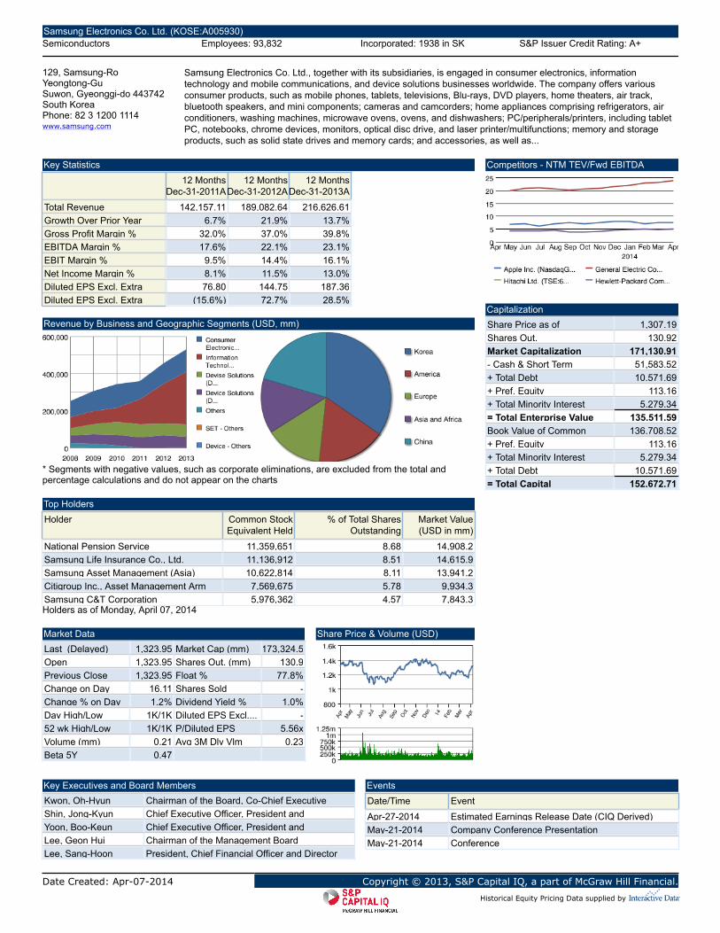
Date Created: Apr-07-2014 Copyright © 2013, S&P Capital IQ, a part of McGraw Hill Financial.Historical Equity Pricing Data supplied by
Samsung Electronics Co. Ltd. (KOSE:A005930)Semiconductors Employees: 93,832 Incorporated: 1938 in SK S&P Issuer Credit Rating: A+
129, Samsung-RoYeongtong-GuSuwon, Gyeonggi-do 443742South KoreaPhone: 82 3 1200 1114www.samsung.com
Samsung Electronics Co. Ltd., together with its subsidiaries, is engaged in consumer electronics, informationtechnology and mobile communications, and device solutions businesses worldwide. The company offers variousconsumer products, such as mobile phones, tablets, televisions, Blu-rays, DVD players, home theaters, air track,bluetooth speakers, and mini components; cameras and camcorders; home appliances comprising refrigerators, airconditioners, washing machines, microwave ovens, ovens, and dishwashers; PC/peripherals/printers, including tabletPC, notebooks, chrome devices, monitors, optical disc drive, and laser printer/multifunctions; memory and storageproducts, such as solid state drives and memory cards; and accessories, as well as...
Key Statistics12 Months
Dec-31-2011A12 Months
Dec-31-2012A12 Months
Dec-31-2013A
Total Revenue 142,157.11 189,082.64 216,626.61Growth Over Prior Year 6.7% 21.9% 13.7%Gross Profit Margin % 32.0% 37.0% 39.8%EBITDA Margin % 17.6% 22.1% 23.1%EBIT Margin % 9.5% 14.4% 16.1%Net Income Margin % 8.1% 11.5% 13.0%Diluted EPS Excl. ExtraItems
76.80 144.75 187.36Diluted EPS Excl. ExtraItems...
(15.6%) 72.7% 28.5%
Revenue by Business and Geographic Segments (USD, mm)
* Segments with negative values, such as corporate eliminations, are excluded from the total andpercentage calculations and do not appear on the charts
Top HoldersHolder Common Stock
Equivalent Held% of Total Shares
OutstandingMarket Value(USD in mm)
National Pension Service 11,359,651 8.68 14,908.2Samsung Life Insurance Co., Ltd. 11,136,912 8.51 14,615.9Samsung Asset Management (Asia)Limited
10,622,814 8.11 13,941.2Citigroup Inc., Asset Management Arm 7,569,675 5.78 9,934.3Samsung C&T Corporation 5,976,362 4.57 7,843.3Holders as of Monday, April 07, 2014
Market DataLast (Delayed) 1,323.95 Market Cap (mm) 173,324.5Open 1,323.95 Shares Out. (mm) 130.9Previous Close 1,323.95 Float % 77.8%Change on Day 16.11 Shares Sold
Short...-
Change % on Day 1.2% Dividend Yield % 1.0%Day High/Low 1K/1K Diluted EPS Excl.... -52 wk High/Low 1K/1K P/Diluted EPS
Before...5.56x
Volume (mm) 0.21 Avg 3M Dly Vlm(mm)
0.23Beta 5Y 0.47
Share Price & Volume (USD)
Competitors - NTM TEV/Fwd EBITDA
CapitalizationShare Price as ofApr-04-2014
1,307.19Shares Out. 130.92Market Capitalization 171,130.91- Cash & Short TermInvestments
51,583.52+ Total Debt 10,571.69+ Pref. Equity 113.16+ Total Minority Interest 5,279.34= Total Enterprise Value(TEV)
135,511.59Book Value of CommonEquity
136,708.52+ Pref. Equity 113.16+ Total Minority Interest 5,279.34+ Total Debt 10,571.69= Total Capital 152,672.71
Key Executives and Board MembersKwon, Oh-Hyun Chairman of the Board, Co-Chief Executive
Officer and...Shin, Jong-Kyun Chief Executive Officer, President andRepresentative...Yoon, Boo-Keun Chief Executive Officer, President andRepresentative...Lee, Geon Hui Chairman of the Management Board
Lee, Sang-Hoon President, Chief Financial Officer and Director
EventsDate/Time Event
Apr-27-2014 Estimated Earnings Release Date (CIQ Derived)May-21-2014 Company Conference PresentationMay-21-2014 Conference

Date Created: Apr-07-2014 Copyright © 2013, S&P Capital IQ, a part of McGraw Hill Financial.Historical Equity Pricing Data supplied by
Sony Corporation (TSE:6758)Consumer Electronics Employees: 162,700 Incorporated: 1946 in JN S&P Issuer Credit Rating: BBB-
1-7-1 KonanMinato-kuTokyo 108-0075JapanPhone: 81 3 6748 2111www.sony.net
Sony Corporation designs, develops, manufactures, and sells electronic equipment, instruments, and devicesfor consumer, professional, and industrial markets worldwide. It offers consumer products and devices, such asLCD televisions; home and car audio, Blu-ray disc and DVD players/recorders, and memory-based portable audiodevices; compact digital, home-use video, and interchangeable single-lens cameras; and personal computers. Thecompany also develops, produces, markets, and distributes PlayStation3, PlayStation Vita, PlayStation Portable,and PlayStation 2 hardware and related software. In addition, it provides professional devices and solutions, such asbroadcast- and professional-use products, and other B2B business solutions; CMOS image...
Key Statistics12 Months
Mar-31-2012A12 Months
Mar-31-2013A12 Months
Dec-31-2013A12 Months
Mar-31-2014E12 Months
Mar-31-2015E
Total Revenue 78,499.12 71,902.11 72,334.89 74,901.51 75,012.67Growth Over Prior Year (9.9%) 4.7% 14.5% 13.4% 0.3%Gross Profit Margin % 20.8% 21.2% 22.5% - -EBITDA Margin % 4.0% 4.4% 4.6% 5.6% 7.4%EBIT Margin % (0.1%) 0.3% 1.0% - -Net Income Margin % (7.1%) 0.6% 1.4% - -Diluted EPS Excl. ExtraItems
(5.52) 0.43 0.84 (0.94) 0.58
Revenue by Business and Geographic Segments (USD, mm)
* Segments with negative values, such as corporate eliminations, are excluded from the total andpercentage calculations and do not appear on the charts
Top HoldersHolder Common Stock
Equivalent Held% of Total Shares
OutstandingMarket Value(USD in mm)
Mitsubishi UFJ Asset Management Co.,Ltd.
57,073,992 5.50 1,100.5Sumitomo Mitsui Trust AssetManagement Co.,...
52,277,924 5.04 1,008.0BlackRock, Inc. 46,370,968 4.47 894.1Credit Suisse, Investment Banking and... 35,802,079 3.45 690.3Waddell & Reed Investment ManagementCo.
26,512,000 2.55 511.2Holders as of Monday, April 07, 2014
Market DataLast (Delayed) 18.96 Market Cap (mm) 20,007.9Open 19.04 Shares Out. (mm) 1,037.7Previous Close 19.28 Float % 64.9%Change on Day (0.32) Shares Sold
Short...-
Change % on Day (1.7%) Dividend Yield % 1.3%Day High/Low 19.0/18.8 Diluted EPS Excl.... 0.8552 wk High/Low 23.4/14.6 P/Diluted EPS
Before...22.17x
Volume (mm) 3.99 Avg 3M Dly Vlm(mm)
14.16Beta 5Y 1.11
Share Price & Volume (USD)
EPS Estimate (USD)
EstimatesRecommendation Outperform(2.20)Target Price 20.02046830LT Growth % 17.00%
Forward MultiplesFY2014 FY2015
P/E NM 33.51xTEV/REV 0.43x 0.42xTEV/EBITDA 7.61x 5.75xPEG NM 1.97x
Competitors - NTM TEV/Fwd EBITDA
CapitalizationShare Price as ofApr-04-2014
18.96Shares Out. 1,037.68Market Capitalization 19,678.00- Cash & Short TermInvestments
5,818.58+ Total Debt 12,510.51+ Pref. Equity -+ Total Minority Interest 4,945.09= Total Enterprise Value(TEV)
31,315.02Book Value of CommonEquity
23,061.82+ Pref. Equity -+ Total Minority Interest 4,945.09+ Total Debt 12,510.51= Total Capital 40,517.41
Key Executives and Board MembersNagayama, Osamu Chairman of the Board and Member of
Nominating...Hirai, Kazuo Chief Executive Officer, President,Representative...Kato, Masaru Vice Chairman, Member of NominatingCommittee and...Morita, Akio Co-Founder
Yoshida, Kenichiro Chief Financial Officer, Executive Vice Presidentand...
EventsDate/Time Event
May-09-2014 Estimated Earnings Release Date (CIQ Derived)Sep-14-2014 End of Lock-Up Period

1
Appendix C: Woodside Capital Partners Contact Information
Hardware and Semiconductors Team
Rudy Burger Greg Mischou Managing Partner Senior Partner [email protected] [email protected] 650‐513‐2755 650‐513‐2757
Mike Powell Shusaku Sumida Partner and Managing Director Managing Director [email protected] [email protected] +44 0208 144 5139 650‐513‐2760
Kirk Bloede [email protected]‐513‐2761
Software and Internet Services Team
Kelly Porter Tricia Salinero Managing Director / Co‐Head Managing Director / Co‐Head [email protected] [email protected] 650‐513‐2756 650‐513‐2758
Ron Heller Indu Navar Managing Director Managing Director [email protected] [email protected] 650‐513‐2762 650‐513‐2774
Special Situations
Jon Thomas Managing [email protected] 650‐513‐2763
Research Team
Sean Blakley Sam Skinner Managing Director Chief Operating Officer [email protected] [email protected] 707‐570‐6512 650‐513‐2759
Ed Bierdeman Ryan Koontz Managing Director Managing Director [email protected] [email protected] 650‐513‐2780 650‐513‐2778
Marshall SenkManaging Director [email protected]‐513‐2781