Embed Size (px)
Citation preview

Preliminary EM4294
Copyright 2006, EM Microelectronic-Marin SA 1 www.emmicroelectronic.com
13.56MHz Crypto Analogue Front End Circuit
For High Secure RFID communication
General Description
The EM4294 is an analogue front end for high secure 13.56MHz RFID reader systems. The reader integrates the crypto algorithm of the EM4035 transponder IC associated with 4 secret keys. Each secret key is 96 bit length and it gives access to the EM4035 tag protected memory after a true mutual authentication process between the tag and the reader. The secret key can not be read by an external device and their integrity is protected by a 32 bit password. The reader IC incorporates also 40k Bytes of user free memory accessible through an ISO7816-3 serial line. The EM4294 RF blocks are similar to the EM4094 one and have the same parameters and performances. The EM4294 reader chip can be used in different systems having sub carrier frequencies from 212kHz to 848kHz, hence covering ISO14443 and ISO15693 and Sony Felica
TM protocols.
The EM4294 offers several options for the RF communication which options can be adapted using a 3 wire serial interface. The push-pull transmitter generates 200mW output RF
power into a 50Ω load. The RF output stage drivers are capable of OOK or ASK modulation from 7% up to 30% of AM modulation. The EM4294 operating voltage is comprised between 3.3V and 5V.
Applications Electronic metering (gas, water, etc…) Vending machines, e-payments Public transportation Secure access control (fitness, swimming pools, etc) Low cost desktop reader / terminal (hotels, etc…)
Features
ISO15693 & ISO14443 Type A and B compatible HF EPC compliant Supports Sony Felica
TM protocol
8 Bytes serial unique ID number containing a customer code
Integrates EM4035 Crypto algorithm 4 secret keys of 96 bit length (write mode only) 32 bit password to change secret key contents Ratification number to prevent against attacks Random generator flips 140-2 compliant 40k Bytes of user free memory 3.3V or 5V Power Supply (analogue and digital) Antenna driver using OOK or ASK modulation ASK modulation index adjustable from 7% - 30% Single or double antenna driver configuration High output RF power of 200mW from 5V supply Antenna short circuit protection 2 receiver inputs for AM and PM demodulation 848KHz BPSK internal decoder (ISO14443 type B) Reception chain compliant with 212kHz, 424kHz,
484kHz and 848kHz sub-carriers Reception chain compliant with Manchester, Miller,
and BPSK data encodings Built-in receive low-pass filter which cut-off
frequencies are selectable between 400kHz and 1MHz
Built-in receive high-pass filter cut-off frequency selectable between 100kHz, 200kHz and 300kHz
Selectable receive gain from 0dB up to 40dB Serial 3 pins interface for option selection Power down mode controlled by the 3 wires SPI
Operation temperature range -40°C to +85°C
SO24 Package
Typical Application
C1
150pF
C101uF
INTERFACE
VCC
VCC
C410pF
C14100nF
RFIN1C5
47pF
DVDDA2
I/O
C822pF
ANT2
Antenna
C9100nF
RFIN2
RST
AGD
DVDDA1
13.56MHz
CRYPTO
VDD
DVSS
C2
120pF
L1
1uH
C3470pF
VSSEN
OSCOUT
CLK
C12100nF
DIN
OSCIN
DOUT
DCLK
C131uF
C722pF
INTERFACE
C11100nF
SPI
VCC
DOUT1
ANT1
C610nF
VCC
EM MICROELECTRONIC - MARIN SA

Preliminary EM4294
Copyright 2006, EM Microelectronic-Marin SA 2 www.emmicroelectronic.com
TABLE OF CONTENTS
1. BLOCK DIAGRAM..........................................................................................................................................4
2. HANDLING PROCEDURES .............................................................................................................................4
3. ABSOLUTE MAXIMUM RATINGS ....................................................................................................................4
3.1 ABSOLUTE MAXIMUM RATINGS............................................................................................................................................... 4 3.2 LATCH-UP PROTECTIONS ...................................................................................................................................................... 5 3.3 OPERATING CONDITIONS....................................................................................................................................................... 5 3.3 ELECTRICAL CHARACTERISTICS ............................................................................................................................................. 5 3.4 TIMING CHARACTERISTICS..................................................................................................................................................... 7 3.5 USER FREE MEMORY CHARACTERISTICS ................................................................................................................................ 7
4. EM4294 FUNCTIONAL DESCRIPTION ............................................................................................................8
5. RF TRANSCEIVER FUNCTIONAL DESCRIPTION..........................................................................................8
5.1 POWER SUPPLY (VDD & VSS) ............................................................................................................................................. 8 5.2 POWER MANAGEMENT........................................................................................................................................................... 8 5.3 DRIVER POWER SUPPLY (VDDA1, VSSA1 & VDDA2, VSSA2) .............................................................................................. 8 5.4 BAND-GAP REFERENCE......................................................................................................................................................... 8 5.5 INTERNAL OSCILLATOR.......................................................................................................................................................... 8 5.6 ANTENNA DRIVERS................................................................................................................................................................ 8 5.7 MODULATOR ........................................................................................................................................................................ 8 5.8 RECEIVER............................................................................................................................................................................ 9 5.9 BPSK DECODER.................................................................................................................................................................. 9 5.10 AGC SYSTEM................................................................................................................................................................... 10 5.11 SERIAL INTERFACE ........................................................................................................................................................... 10
6. OPTION BITS...................................................................................................................................................11
7. OPTION BITS SELECTION DEPENDING TRANSPONDER IC .....................................................................13
7.1 EM4006 READ ONLY: ........................................................................................................................................................ 13 7.3 ISO14443 TYPE A:............................................................................................................................................................ 14 7.4 ISO14443 TYPE B:............................................................................................................................................................ 14 7.5 ISO14443 TYPE C, SONY FELICA
TM: .................................................................................................................................. 15
8. SERIAL INTERFACE ISO7816-3 DESCRIPTION...........................................................................................15
8.1 SERIAL INTERFACE ISO7816-3 DEFINITION ........................................................................................................................... 15 8.2 SERIAL INTERFACE ISO7816-3 TIMINGS ............................................................................................................................... 15
8.2.1 Cold reset .............................................................................................................................................15 8.2.2 Warm reset ...........................................................................................................................................16 8.2.3 ISO7816-3 Guard times .......................................................................................................................16 8.2.4 Character level timings.........................................................................................................................17
9. EM4035 CRYPTO MODULEDESCRIPTION...................................................................................................17
9.1 APDU COMMAND SET ........................................................................................................................................................ 18 9.1.1 ATR ......................................................................................................................................................18
9.2 APDU KEY MANAGEMENT .................................................................................................................................................. 18 9.2.1 Enter Password for Key update............................................................................................................18 9.2.2 Set New Password ...............................................................................................................................18 9.2.3 Key Update...........................................................................................................................................18
9.3 APDU EDDY MUTUAL AUTHENTICATION ............................................................................................................................... 19 9.3.1 Select Authentication Key ....................................................................................................................19 9.3.2 Send A1 random number .....................................................................................................................19 9.3.3 Get A2 random number and f() function response...............................................................................19 9.3.4 Send g() function ..................................................................................................................................20
9.4 EXTENDED USER COMMAND SET ......................................................................................................................................... 21 9.4.1 Get Chip Supplier Serial Number (CSSN) ...........................................................................................21 9.4.2 Get Random number ............................................................................................................................21 9.4.3 System Commands ..............................................................................................................................21

Preliminary EM4294
Copyright 2006, EM Microelectronic-Marin SA 3 www.emmicroelectronic.com
9.4.4 Read User Memory (EEPROM) ...........................................................................................................22 9.4.5 Write User Memory (EEPROM) ...........................................................................................................22
9.5 IMPLEMENTATION................................................................................................................................................................ 22 9.5.1 Memory Mapping..................................................................................................................................22 9.5.2 Security level ........................................................................................................................................22 9.6 Power Consumption indications ..............................................................................................................22
10 . ANTENNA CONNECTION CONFIGURATIONS..........................................................................................23
10.1 SINGLE OUTPUT DRIVER (100MW) .................................................................................................................................... 23 10.3 CONFIGURATION FOR LOWER POWER SYSTEMS WITH DIRECT ANTENNA CONNECTION ............................................................... 24
11. 3.3V OPERATING VOLTAGE ............................................................ERROR! BOOKMARK NOT DEFINED.
12. PIN CONFIGURATION ..................................................................................................................................25
13. PIN DESCRIPTION ........................................................................................................................................25
14. PACKAGE INFORMATION ...........................................................................................................................26
15. ORDERING INFORMATION..........................................................................................................................26
16. PRODUCT SUPPORT....................................................................................................................................26
Preliminary EM4294
Copyright 2006, EM Microelectronic-Marin SA 4 www.emmicroelectronic.com
1. Block Diagram
Figure 2
2. Handling Procedures This device has built-in protection against high static voltages or electric fields; however, anti-static precautions must be taken as for any other CMOS component. Unless otherwise specified, proper operation
can only occur when all terminal voltages are kept within the voltage range. Unused inputs must always be tied to a defined logic voltage level.
3. Absolute Maximum Ratings 3.1 Absolute Maximum Ratings VSS = 0V
Parameters Symbol Conditions
Maximum voltage at VDD VVDDMAX VVSS
+6V
Minimum voltage at VDD VVDDMIN VVSS
-0.3V
Max. voltage other pads VMAX
VVDD
+0.3V
Min. voltage other pads VMIN
VVSS
-0.3V
Max. junction temperature TJMAX
+125°C
Storage temperature range TSTO
-40 to +125°C
Electrostatic discharge max. to MIL-STD-883 method 3015 ref VSS VESD
2KV
Electrostatic discharge max. to MIL-STD-883 method 3015 for pins ANT1 & ANT2
VESDANT 4KV
Maximum Input / Output current on all pads except VDD, VDDA1, VDDA2, VSS, VSSA1, VSSA2, ANT1 and ANT2
IIMAX
IOMAX
10mA
Maximum AC peak current on VDDA1, VDDA2, VSSA1, VSSA2, ANT1 and ANT2 pads at 13MHz, duty cycle 50% (per antenna driver)
IANTMAX
100mA
RST, CLK, I/O ISO pins ( HBM +/- 4kV, 5.5V, 25°C) ILeak ISO
1 +/- 100nA
Table 1
Stresses above these listed maximum ratings may cause permanent damages to the device. This is a stress rating only and functional operation of the device at these or at any other conditions above those indicated in the operation section of this specification is not implied. Exposure beyond specified operating conditions may affect device reliability or cause malfunction. Note 1: procedure MILSTD-883 D Method 3015.7, pin to pin, pin to Vss, pin to VDD
EM4035 CRYPTO
ALGORITHM
4 SECRET KEYS
40K BYTES USER FREE
MEMORY
SERIAL INTERFACE
OPTION BITS
DVDDA1
DVDDA2
VSSA2 VSSA1
ANT1
ANT2
RFIN1 RFIN2
I/O
CLK
RST
EN
MODULATOR
ANTENNA DRIVER
ANTENNA DRIVER
DEMODULATOR
FILTER GAIN
COMPARATOR
OSCILLATOR
BPSK DECODER
OSCIN OSCOUT
DIN DOUT DOUT1 DCLK

Preliminary EM4294
Copyright 2006, EM Microelectronic-Marin SA 5 www.emmicroelectronic.com
3.2 Latch-Up Protections Pads are qualified according to JEDEC 778 class I level A specifications. 3.3 Operating Conditions
Parameters Symbol Min. Typ. Max. Units
Power supply voltage VVDD 3 3.3 / 5 5.5 V
Operating junction temperature TJ -25 +110 °C
Package Thermal resistor for SO24W (note 1) RthJ-A °C/W
Op ext clock frequency (CLK input) Fclk 5 MHz
Op ext clock duty cycle (CLK input) Dclk 40 60 %
Load impedance on ANT1 or ANT2 drivers ZANT (7+j0) Ω
Quartz load capacitors (note 2) C1 & C2 2 x 22pF
Capacitors VDDA1, VSSA1 filtering (note 2) C7, C8 & C10 1nF, 100nF and 10µF connected in parallel
Capacitors VDDA2, VSSA2 filtering (note 2) C5, C6 & C9 1nF, 100nF and 10µF connected in parallel
Capacitors VDD, VSS filtering (note 2) C11 & C12 1nF, 100nF connected in parallel
AGD filtering capacitors (note 2) C13 100nF (optional 1nF in parallel) Table 2
Note 1: The maximum operating temperature is calculated with the following formula: Ta = (RThja * P) - Tjmax
Tj: maximum junction temperature Ta: ambient temperature Note 2: For the capacitors, refer to the Typical Application schematic on the first page of the datasheet.
The Quartz load capacitors are in COG ceramic technology (±5%)
Use COG ceramic technology (±5%) for the 1nF capacitors.
Use X7R ceramic technology (±10%) for the 100nF capacitors.
Use tantalum electrolytic technology for the 10µF capacitors. The package thermal resistors are based on a multi-layer test board and zero airflow. The package performance is highly dependent on board and environmental conditions. 3.3 Electrical Characteristics Unless otherwise specified: VVSS = VVSSA1 = VVSSA2 = 0V & VVDD = VVDDA1 = VVDDA2 = 5V, TJ= -40 to +110°C.
Parameters Symbol Test Conditions Min Typ Max Units
General DC parameters Supply current in power-down mode
IPD
1 5 µA
Supply current excluding antenna driver current
ION
Option bits value: 04800001 (Hexa)
12 20 mA
AGD level VAGD
2.3 2.5 2.7 V
Power on reset level VPOR 1.4 2.1 3.6 V Antenna Drivers
ANT1 (or ANT2) driver output impedance
RAD
IANT = 100mA
100% modulation index 3 7 12 Ω
ANT1 (or ANT2) driver output impedance
RAD
IANT = 100mA
10% modulation index 5 10 15 Ω
Serial Interface
Input logic low VIL 0.2VDD V
Input logic high VIH
0.8VDD V
Output logic high VOH
ISOURCE
= 1mA 0.9VDD V
Output logic low VOL
ISINK
= 1mA 0.1VDD V
Maximum serial interface clock frequency
Fmax 1 MHz
AM demodulation
RF amplitude at RFIN inputs VRFIN 2.5 VVDD VPP RFIN input resistance RRFIN
5 10 20 kΩ Receiver sensitivity @ 212kHz (note 3) 1.5 3 mVpp Receiver sensitivity @ 424kHz (note 3) 2.2 4.5 mVpp Receiver sensitivity @ 848kHz VSENS (note 3) 3.5 6 mVpp
Power on Reset UVD2.5=
POR-VTH2.5 2.55 2.6 2.65 V

Preliminary EM4294
Copyright 2006, EM Microelectronic-Marin SA 6 www.emmicroelectronic.com
EM4035 CRYPTO Algorithm Module
Parameters Symbol Test Conditions Min Typ Max Units
Supply current idle clock stop IccS_hV
VDD max CLK=1MHz, 25°C 70 100 µA
Supply current idle IccI_hV
VDD max CLK=1MHz, 25°C 115 150 µA
Supply current at high speed 6 10 mA Note 3: Sine wave envelope, max. gain, RF amplitude in VRFIN
I/O pin of EM4035 Crypto Modulein reception mode When in reception mode, and with the supply voltage (VDD) in the range specified in Table 2, the I/O of the EM4035 Crypto Moduleshall correctly interpret signals from the terminal having the characteristics shown in the table below:
Parameters Symbol Test Conditions Min Max Units
H Input Voltage VIH
0.7 x VDD VDD+0.3V V
L Input Voltage VIL hv
mv
-0.3
-0.3
0.8
0.2 x VDD
V
V
Rise Fall Time tR and t
F Cin =Cout =30pF,
VDD=VDDmax 1.0 µs
Input leakage IIL 0V <Vin< VDD,
VDD=VDDmax -20 20 µA
Note 4: The ICC shall not be damaged by overshoot or undershoot on the I/O line in the range –0.3 V to VDD + 0.3 V.
I/O pin of EM4035 Crypto Modulein transmission mode When in transmission mode, the I/O of the EM4035 Crypto Moduleshall send data to the terminal with the characteristics shown in shown in the table below:
Parameters Symbol Test Conditions Min Max Units
H Output Voltage VOH
(note5) 0 < IOH < 1 mA, VDD = min. 0.7xVDD VDD V
L Output Voltage VOL 0 < IOL < 1 mA, VDD = min.
hv, mv range
0
0.4
V
Rise Fall Time tR and tF CIN (terminal) = 30 pF max.
VDD=VDDmin, 10% to 90% - 1.0 µs
Note 5: The pull-up resistor is disconnected. Unless transmitting, the EM4035 Crypto Modulesets its I/O line driver to reception mode. There is no requirement for the EM4035 Crypto Moduleto have any current source capability from I/O.
Clock (CLK) pin of EM4035 Crypto module With VDD in the range specified in table 2, the clock of the EM4035 Crypto Moduleshall operate correctly with a CLK signal having the characteristics shown in the table below:
Parameters Symbol Test Conditions Min Max Units
H Input Voltage VIH 0.7 x VDD VDD+0.3V V
L Input Voltage VIL hv
mv
-0.3
-0.3
0.5
0.2 x VDD
V
V
Rise Fall Time tR and tF VDD = min. to max.
Tiso_clk=1µs max
- 9% of clock period
µs
Input leakage IIL 0V <Vin< VDD, VDD=VDDmax
-20 20 µA

Preliminary EM4294
Copyright 2006, EM Microelectronic-Marin SA 7 www.emmicroelectronic.com
Reset (RST) pin of EM4035 Crypto module With VDD in the range specified in Table 2-1, the clock of the EM4035 Crypto Moduleshall correctly interpret a RST signal having the characteristics shown in the table below:
Parameters Symbol Test Conditions Min Max Units
H Input Voltage VIH 0.8 x VDD VDD+0.3V V
L Input Voltage VIL hv
mv
-0.3
-0.3
0.6
0.2 x VDD
V
V
Rise Time tR VDD = min. to max. - 400 µs
Fall Time tF VDD = max. to min. - 1.0 µs
Input leakage IIL 0V<Vin< VDD, VDD=VDDmax
-20 20 µA
3.4 Timing Characteristics Unless otherwise specified: VVSS = VVSSA1 = VVSSA2 = 0V & VVDD = VVDDA1 = VVDDA2 = 5V, TJ= -40 to +110°C.
Parameters Symbol Test Conditions Min Typ Max Units
Xtal Oscillator
Normal mode (note 4) 0.3 0.9 1.6 mS Transconductance gm
Hi oscillator mode (note 4) 1.5 2.7 4.0 mS
Set-up time after power down Tset 5 15 Ms
AM demodulation
Recovery time of reception after antenna modulation
Trec 100 µs
Table 4
Note 4: It is recommended to use the high gm transconductance. Crystal electrical parameters: Quality factor min: 26000
Series resistance typ: 20Ω Static capacitance typ: 2.8pF 3.5 User Free Memory Characteristics
Parameters Symbol Test Conditions Min Max Units
Retention NVM retention
Mass erase pattern, 250°C, active margin
72 hours
Mass erase time NVM-Tmer (SW)
20 ms
Write time NVM-T write
40 us
Endurance Page erase Byte program
GP NVM endurance
25°C 100
Page erase time GP NVM-Tper (HW)
128 Bytes / Page 2
Cumulative Program GP NVM
cumul prog Number of write per byte
without erase - 1

Preliminary EM4294
Copyright 2006, EM Microelectronic-Marin SA 8 www.emmicroelectronic.com
4. EM4294 Functional Description The EM4294 crypto analogue front end is mainly composed by three major parts: RF transceiver structure to send commands to the tag
and receive back the its message. Crypto block that contains the secure EM4035 crypto
algorithm, the 4 secret keys and the random generator. User free memory that can be used to store extra
information on the system (for ie tags UID).
5. RF Transceiver Functional Description 5.1 Power Supply (VDD & VSS) The EM4294 analogue front end can operate at 3.3V or 5V. The power supply voltage has to be the same on the analogue and digital input lines (VDD, VDDA1, VDDA2). It is strongly recommended to use a regulated supply. Power supply ripples and noise, inside the receiver frequency range, degrades the overall system performances. To use the EM4294 at 3.3V, an external resistor has to be connected on the AGD output to fix a voltage of 2.0V on AGD. The external resistor can be switched off (using for example a microcontroller I/O) when the reader chip is not used. 5.2 Power management There are two available power modes. The selection of these two modes is done with the Power up Flag (option bit 1). There are two ways to put the EM4294 Analog Front End in a power down state: Reseting the power up flag. Applying a low level on EN input. In that case, only
the analog circuitry goes to Power Down but the SPI interface remains active.
When EN is changed to high (and power up flag is high) the EM4294 goes immediately to the mode in which it was before EN went low level. In power-up mode, the oscillator is started followed by the transmitter and the receiver. When the chip is ready to operate (quartz oscillator, receiver operating points are ready and transmitter is not shorted (if bit 5 is set) a
100µs ready pulse is generated on DOUT pin. After that condition, the chip goes to normal operation mode. DOUT corresponds to the demodulated signal output and DOUT1 is the 13.56MHz-clock output (if DOUT1 is not used as BPSK clock output in ISO14443 type B standard). 5.3 Driver Power Supply (VDDA1, VSSA1 & VDDA2, VSSA2) Supply lines should be separately filtered for analogue chip supply and antenna driver supplies.
Any variations in supply voltage directly modulate the antenna driver and they are fed to the receiver’s input. The power supply sensitivity range, for frequency components which are in the receiving bandwidth, is the same as the RFIN sensitivity.
5.4 Band-Gap reference The reference voltage (2.5V) is generated internally by a Band-gap reference and uses an external capacitor for blocking. 5.5 Internal Oscillator The oscillator is driven by the13.56MHz external crystal to generate the RF frequency. The external quartz crystal is connected to the load capacitors as indicated in Figure 1. It is also possible to apply an external clock source, DC coupled to OSCIN, according to Vi input levels, to drive the internal oscillator. When option bit 27 is set, OSCIN corresponds to the digital input of the internal oscillator. The oscillator start-up time can be decreased by setting option bit 26 (oscillator gain). 5.6 Antenna drivers The antenna driver produces the RF signal from the oscillator output. The PMOS and NMOS driver side are fed by non-overlapping signals (3ns) to minimize the power consumption. The output resistance of each antenna driver is typically
7Ω. It is changed, during the field modulation, to set the right ASK modulation index level (option bits 2, 3, 4). The two integrated antenna drivers can be used in three possible configurations depending on the output power level (refer to application chapter on page 11). When a single driver configuration is selected, the output
power level on the 50Ω load is 100mW. For a 200mW output power, both drivers have to be used in parallel configuration to double the output power (option bit 6). The drivers can operate in push-pull configuration (option bit 7). This mode can be used in case of direct antenna connection. In that configuration, the reader antenna is connected to the output drivers through a resonant capacitor (LC tank adjusted to 13.56MHz) Take note that, in direct antenna configuration, the output power can exceed 200mW. Chip cooling requirements must be carefully considered. To be compliant with national country regulations, it could be necessary to add a filtering structure between the IC output stage drivers and the antenna. For more information, please, refer to the product application note. The short protection circuit (option bit 5) prevents damage to the output driver when the ANT pin is shorted to ground or to the power supply. 5.7 Modulator The modulator enables OOK or ASK modulation of the RF signal on the antenna outputs (ANT1 and ANT2). When the device is in normal mode, DIN corresponds to the modulator input. A high input level, on DIN input, causes a low field (ASK modulation index) or a field-stop if OOK modulation is chosen.

Preliminary EM4294
Copyright 2006, EM Microelectronic-Marin SA 9 www.emmicroelectronic.com
Upper trace: digital input (DIN) modulation input
Lower trace: transmitted field on ANT1 for ie Reader modulation is set to OOK (100% AM)
Upper trace: digital input (DIN) modulation input
Lower trace: transmitted field on ANT1 for ie Reader modulation is set to 16% ASK
The selection between OOK and ASK modulation depth is done using configuration bits 2, 3 and 4. The field modulation index can be adjusted from 7% up to 30% covering all the ISO standard air interface requirements. Before and after a modulation phase, the receiver input is disconnected from the antenna circuitry to preserve DC operating point setting. For high quality factor systems, it may be necessary to prolong (option bit 25) the hold time after modulation to allow settling of the resonant circuit. 5.8 Receiver The receiver senses the envelope of the signal present on the inputs RFIN1 or RFIN2 (option bit 14). These two inputs, used with external components, permit the detection of amplitude or phase modulated signals. Any RF frequency components still present in the envelope signal are removed by a second order low pass filter. The received signal DC component is removed by the high pass filter, which has selectable corner frequency (option bits 8 and 9). The signal is amplified and further processed by the low pass filtering stage, which corner frequency is selectable (option bit 10). The gain selection (option bits 11, 12 and 13) should be chosen according to the reader system parameters.
Modifying the signal bandwidth changes noise level and results in different input sensitivity. These three bits define 8 gain settings according to the option bit table. The total gain range is 40dB. The output signal, in normal mode, can be a digitized sub-carrier, a 106kbit/s BPSK decoded bit stream (DOUT) or an analogue output used for DSP decoding (DOUT1). When a direct sub-carrier signal is selected, the tag answer is displayed on the DOUT pin. In such configuration, DOUT1 corresponds to the 13.56MHz clock output, which can be used for synchronization of an external micro-controller used for decoding. 5.9 BPSK Decoder The internal BPSK decoder is designed to decode the transponder's sub-carrier signal according to the ISO14443-type B coding procedure described in the ISO 14443-B standard. First 80 pulses are used as start of frame. The initial Phase State of the sub-carrier is defined as logical "1" and the first phase transition represents a change from logical "1" to logical "0". The sub-carrier frequency is 13.56MHz divided by 16 and each bit period consists of 8 pulses according to ISO14443-B standard. The BPSK decoder is enabled by setting to a high level option bit 22. When this option bit is set, the decoded bit-stream is available on pin DOUT and the bit clock on pin DOUT1. The data is valid on the rising edge of bit clock.
Upper trace: digital output (DOUT1) BPSK clock
Bottom trace: digital output (DOUT) BPSK decoded data
The BPSK decoder decodes the transponder's signal, which can have a frequency offset. The transponders clock extractor can omit or add some clock transitions at modulation. Successful operation, in such conditions, requires a frequency adaptive decoder. When option bit 23 is set, the decoder measures the average frequency of the 80 pulses (SOF) and adjusts the internal shift register to the appropriate length. The decoder is capable of correct operation at incoming bit-stream frequencies of 847.5kHz +/-10%.

Preliminary EM4294
Copyright 2006, EM Microelectronic-Marin SA 10 www.emmicroelectronic.com
When the internal BPSK decoder is not activated and option bit 24 is set, DOUT1 corresponds to the output of the AGC amplifier. 5.10 AGC system The integrated AGC system can be activated via option bit 15. The AGC amplifier has a 40dB gain correction depth. The AGC system is adapted to all RFID communication protocols. Before the transponder starts to emit the data, the receiver gain is set to maximum (option bits 11,12,13). When the reader detects a transponder signal that is above the attack threshold the receiver gain is rapidly reduced (option bits 18 and19) to fit the signal into a linear range of the receiver. The gain remains unchanged as long as the signal level is above the decay threshold. When the received signal falls below the decay threshold for a period of time set by option bits 20 and 21, the reader logic establishes that the communication with one transponder is finished and makes a fast decay to return to the maximum gain. The receiver is ready to demodulate the emission of the next transponder, which can be far away from the reader antenna. This feature is necessary for anti-collision purposes. With transponders that have a modulation DC level shift significantly higher than modulation sub-carrier AC level, the AGC can react on DC shift and decrease the system gain too much. It is possible not to attack the first pulse (option bit 16) in a burst (for OOK modulation) to allow the DC level to settle before AGC action. The time after which the first pulse in a burst is not attacked (shortest sub-carrier stop in OOK modulation is 1/10 of the time) is set by option bits 20, 21 as decay wait time. It is also possible to use slow decay mode (option bit 17). The slow decay is started when the received signal falls below the decay
threshold. The decay rate is one gain step per time defined by option bits 20 and 21. When AGC system is disabled the receiver gain is directly controlled by option bits 11, 12, 13
5.11 Serial Interface The serial interface is used to control the EM4294 option bits setting. A high level on DCLK and a rising edge on DIN reset the serial interface. After the reset, the DIN signal is shifted to the internal register on every rising edge on DCLK. During first 31 DCLK transitions, the DIN data are read to the chip while during the 32nd transition the chip exits the SPI configuration mode and enters the normal mode. In normal mode: DIN is used to modulate the field (high DIN: low
reader filed for ASK or no field for OOK). DCLK must be low in normal mode. DOUT and DOUT1 are data and clock outputs in
normal mode. If the EM4294 reader chip was in power-down mode before entering normal mode (option bit 1 low or pin EN low) the IC goes through a start-up procedure. This means that the quartz oscillator is started (or external clock source is enabled), the output driver is enabled and the antenna drivers are checked for short circuit (if bit 5 is set). After the operation point of the receiver has settled, the
DOUT pin goes high for 100µs and then the chip goes to normal mode. If a short circuit at the antenna driver output is detected, the antenna driver is stopped, DOUT remains low and DOUT1 goes high. If the EM4294 reader IC was powered-up before SPI communication was started it goes directly to the normal mode.
DCLK
DIN
DOUT &DOUT1
SerialInterface
reset
31 Option bits
Selection Option bits mode NormalMode

Preliminary EM4294
Copyright 2006, EM Microelectronic-Marin SA 11 www.emmicroelectronic.com
6. Option Bits Power up flag
Bit 1 Description
0 1
Power down Power up
Output driver configuration: Modulation Index
Bit 4 Bit 3 Bit 2 Description 0 0 0 0 1 1 1 1
0 0 1 1 0 0 1 1
0 1 0 1 0 1 0 1
10% ASK typ. OOK ASK decrease 3% ASK decrease 1.5% ASK increase 3% ASK increase 6% ASK increase 12% ASK increase 20%
Short Circuit Protection
Bit 5 Description 0 1
Short circuit protection disabled Short circuit protection enabled
Single or dual RF driver selection
Bit 6 Description
0 1
ANT1 only ANT1 and ANT2
Dual driver in phase or phase opposite
Bit 7 Description
0 1
In phase driving Differential driving
Receiving Chain Configuration Filter zero selection
Bit 9 Bit 8 Description
0 0 1
0 1 0
High int. zero (~300kHz) Mid. int. zero (~200kHz) Low int. zero (~100kHz)
Filter low pass selection 400kHz
Bit 10 Description
0 1
High cut-off frequency (~1 MHz) Mid. cut-off frequency (~400 kHz)
Receive gain selection 0 (Lsb)
Bit 11 Description
0 1
Nominal gain Gain decreased for 5.7dB
Receive gain selection 1
Bit 12 Description 0 1
Nominal gain Gain decreased for 11.4dB
Receive gain selection 2 (Msb)
Bit 13 Description
0 1
Nominal gain Gain decreased for 22.8dB
AM/PM input channel selection
Bit 14 Description 0 1
RFIN1 input selected RFIN2 input selected

Preliminary EM4294
Copyright 2006, EM Microelectronic-Marin SA 12 www.emmicroelectronic.com
AGC on off selection
Bit 15 Description
0 1
AGC off AGC on
AGC attack mode selection
Bit 16 Description
0 1
Attack always First pulse not attacked
AGC decay mode selection
Bit 17 Description
0 1
Fast decay Slow decay
AGC attack rate
Bit 19 Bit 18 Description
0 0 1
0 1 0
~19 dB/µs (average)
~9.5 dB/µs (average)
~4.7 dB/µs (average)
AGC decay wait
Bit 21 Bit 20 Description
0 0 1
0 1 0
~44µs
~88µs
~176µs
BPSK Decoder Output selection direct sub-carrier or BPSK 848kHz
Bit 22 Description
0 1
Sub-carrier BPSK decoder
BPSK automatic frequency adjust
Bit 23 Description
0 1
Disabled Enabled
Output selection analogue
Bit 24 Description
0 1
Analogue output disabled Analogue output enabled
Bit 25 Description 0 1
Hold delay after modulation ~5µs
Hold delay after modulation ~15µs
Oscillator Oscillator gain selection
Bit 26 Description
0 1
Low gm High gm
External oscillator selection
Bit 27 Description
0 1
Internal quartz oscillator External oscillator
Note: It is recommended to set option bits 16 up to bit 21 and option bits 23, 25 to “0”. Bit 26 should be set to “1”.

Preliminary EM4294
Copyright 2006, EM Microelectronic-Marin SA 13 www.emmicroelectronic.com
7. Option bits selection depending transponder IC The EM4294 transceiver is compliant with almost all 13.56MHz transponder ICs. The large combinations, offered by the EM4294 option bits, permit to adapt the reader IC to the tag communication protocol. The below tables give the suggested option bit configuration depending on the RFID transponder IC used. 7.1 EM4006 Read Only:
Option bit Suggested value Configuration
1 1 Power up 2, 3, 4 1,0,0 OOK modulation
5 1 Short circuit enabled
6, 7 1,0 Two drivers in phase 8, 9 0,1 100kHz
10 1 400kHz 11, 12, 13 0,0,0 Nominal gain
14 0 RFIN1 selected
15 1 AGC activated
16, 17, 18, 19, 20, 21 0,0,0,0,0,0 Standard configuration
22 0 Sub-carrier mode 23 0 BPSK not used
24 0 Analogue output disable
25 0 Hold delay set to 5us
26 1 High gm
27 0 Internal quartz
28, 29, 30, 31 0,0,0,0 Normal IC mode
EM4006 Data rate: 26k Bauds EM4294 Reception bandwidth: 100kHz – 400kHz Configuration word value (Hexa): (msb) 02 00 43 33 (lsb) 7.2 ISO15693 standard and ePC HF protocol:
Option bit Suggested value Configuration
1 1 Power up 2, 3, 4 1,0,0 OOK modulation
5 1 Short circuit enabled 6, 7 1,0 Two drivers in phase
8, 9 0,0 300kHz
10 0 1MHz 11, 12, 13 0,0,0 Nominal gain
14 0 RFIN1 selected 15 1 AGC activated
16, 17, 18, 19, 20, 21 0,0,0,0,0,0 Standard configuration
22 0 Sub-carrier mode
23 0 BPSK not used
24 0 Analogue output disable 25 0 Hold delay set to 5us
26 1 High gm 27 0 Internal quartz
28, 29, 30, 31 0,0,0,0 Normal IC mode
Tag sub-carrier: 424kHz or 484kHz Modulation Index for the reader to tag communication (uplink): 100% Reception bandwidth: 300kHz – 1MHz AGC: Nominal Gain Configuration word value (Hexa): (msb) 02 00 40 33 (lsb)
Preliminary EM4294
Copyright 2006, EM Microelectronic-Marin SA 14 www.emmicroelectronic.com
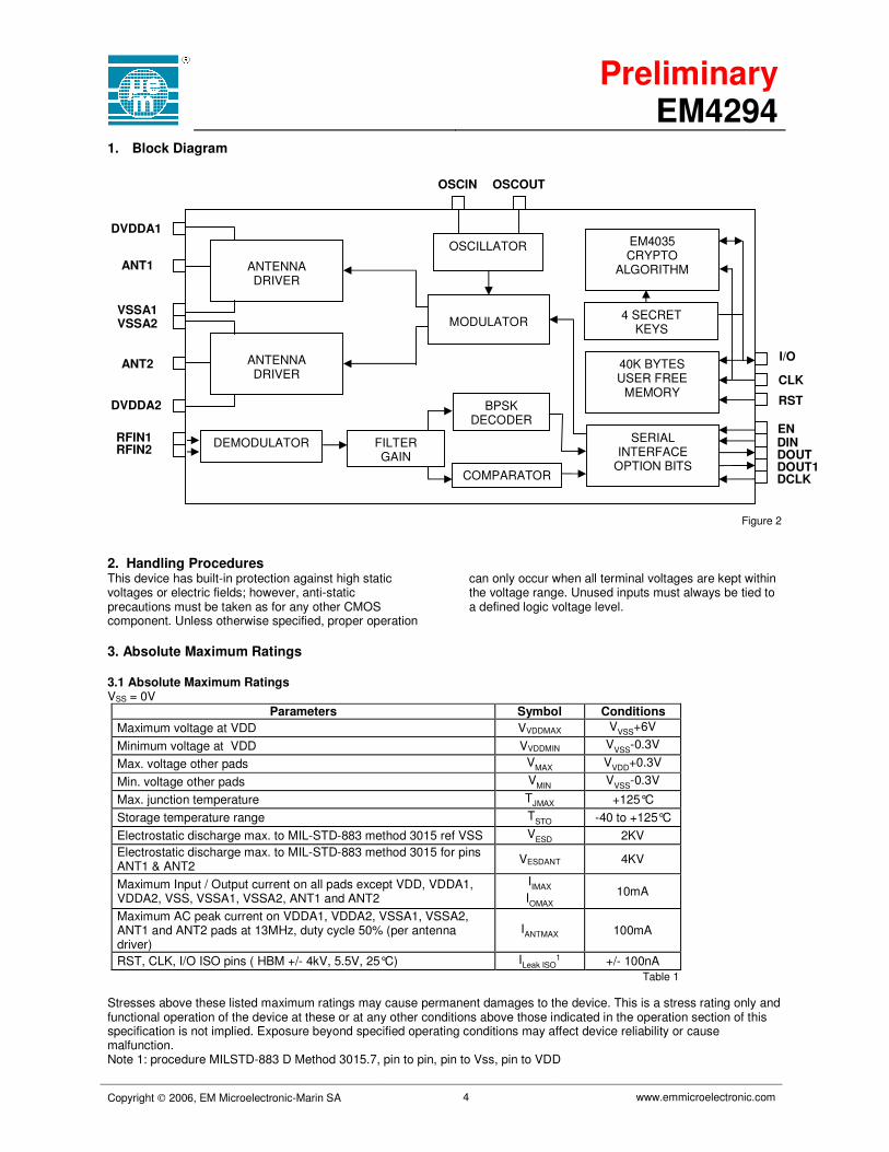
7.3 ISO14443 Type A:
Option bit Suggested value Configuration
1 1 Power up
2, 3, 4 1,0,0 OOK modulation
5 1 Short circuit enabled
6, 7 1,0 Two drivers in phase
8, 9 0,0 300kHz
10 0 1MHz
11, 12, 13 0,0,0 Nominal gain
14 0 RFIN1 selected
15 1 AGC activated
16, 17, 18, 19, 20, 21 0,0,0,0,0,0 Standard configuration
22 0 Sub-carrier mode
23 0 BPSK not used
24 0 Analogue output disable
25 0 Hold delay set to 5us
26 1 High gm
27 0 Internal quartz
28, 29, 30, 31 0,0,0,0 Normal IC mode
Tag sub-carrier: 848kHz Modulation Index: 100% Reception Bandwidth: 300kHz – 1MHz AGC: Nominal Gain Configuration word value (Hexa): (msb) 02 00 40 33 (lsb) 7.4 ISO14443 Type B:
Option bit Suggested value Configuration
1 1 Power up
2, 3, 4 0,0,0 10% ASK
5 1 Short circuit enabled
6, 7 1,0 Two drivers in phase
8, 9 0,0 300kHz
10 0 1MHz
11, 12, 13 0,0,0 Nominal gain
14 0 RFIN1 selected
15 1 AGC activated
16, 17, 18, 19, 20, 21 0,0,0,0,0,0 Standard configuration
22 0 Sub-carrier mode
23 0 BPSK selected
24 0 Analogue output disable
25 0 Hold delay set to 5us
26 1 High gm
27 0 Internal quartz
28, 29, 30, 31 0,0,0,0 Normal IC mode
Tag sub-carrier: 848kHz Modulation Index: 10% Reception bandwidth: 300kHz – 1MHz AGC: Nominal Gain Configuration word value (Hexa): (msb) 02 20 40 31 (lsb)

Preliminary EM4294
Copyright 2006, EM Microelectronic-Marin SA 15 www.emmicroelectronic.com
7.5 ISO14443 Type C, Sony Felica TM
:
Option bit Suggested value Configuration
1 1 Power up
2, 3, 4 0,0,1 13% ASK
5 1 Short circuit enabled
6, 7 1,0 Two drivers in phase
8, 9 0,0 300kHz
10 0 1MHz
11, 12, 13 0,0,0 Nominal gain
14 0 RFIN1 selected
15 1 AGC activated
16, 17, 18, 19, 20, 21 0,0,0,0,0,0 Standard configuration
22 0 Sub-carrier mode
23 0 BPSK not used
24 0 Analogue output disable
25 0 Hold delay set to 5us
26 1 High gm
27 0 Internal quartz
28, 29, 30, 31 0,0,0,0 Normal IC mode
Tag sub-carrier: 250kHz Modulation Index: 13% Reception bandwidth: 300kHz – 1MHz AGC: Nominal Gain Configuration word value (Hexa): (msb) 02 00 40 3D (lsb)
8. Serial Interface ISO7816-3 Description 8.1 Serial Interface ISO7816-3 definition The EM4294 crypto module provides data interface compliant with the ISO 7816-3 specification. This interface is defined to offer the maximum of assistance to software IO routines implementing the different variation of the protocol (Direct/Inverse convention, protocol T=0, T=1, high speed baud rates…). This interface is optimized for high speed supports such as speed enhancement modes in the scope of ISO7816-3 specification and proprietary mode to achieve up to 5 Mbit/s for fast download purpose of EEPROM memories. This interface is intended to work without the need of the CPU during character transmission and reception, therefore it is possible to achieve really low power performances by placing the EM4035 Crypto Modulein idle mode during communications. The EM4294 supports T=0 asynchronous half-duplex character transmission protocol, T=1 asynchronous half duplex block transmission and a proprietary protocol which can be used for fast loading of Code into the OTP by the card manufacturer.
Assignment Symbol EM4294 PINOUT
Reset signal RST RST
Clock signal CLK CLK
Ground GND VSS
Data input/output I/O I/O
8.2 Serial Interface ISO7816-3 timings The session starts with a reset sequence (cold or warm) then a character frame will be issued. A frame is a set of characters generated by the external microcontroller. Frame characteristics include: bit duration, character frame data and character wait times Those timing characteristics dedicated to ISO7816-3 interface involve both hardware and the software implementation; the following table shares requirements between hardware and software.
Item Hardware Software
Cold reset I/O line driver in reception mode timing
Time t1: answer to reset from RST rising edge
Warm reset I/O line driver in reception mode timing
Time t1': answer to reset from RST rising edge
Waiting and guard times
Minimum guard times in Tx at character level are HW performed.
Complementary guard time and waiting time between block and characters shall use Timers configured as ETU counter
Character frame
ISO7816 interface ISO7816 interface programming mode
Bit duration Baud rate generator Baud rate parameters 8.2.1 Cold reset The ISO reset circuit does not differentiate between a cold and a warm reset. If this is required the software must make some provision.

Preliminary EM4294
Copyright 2006, EM Microelectronic-Marin SA 16 www.emmicroelectronic.com
A minimum of 33 clocks cycles is required to get effective reset when RST line is released from ‘0’ to ‘1’. T0 + max 200 cycles: I/O should be in reception mode T1+ t1: ATR should begin between 400 and 45,000 clock cycles
V D D
R S T
C L K
I / O
T 0 T 1
t 1 A n s w e r t o R e s e t I n d e t e r m i n a t e
2 0 0 c y c l e s
Note: t1 is dependant of user software but a minimum value is imposed by Bootrom execution 8.2.2 Warm reset The ISO reset circuit does not differentiate between a cold and a warm reset. If this is required the software must make some provision. A minimum of 33 clocks cycles is required to get effective reset when RST line is released from ‘0’ to ‘1’. T0’ + max 200 cycles: I/O should be in reception mode T1’+ t1’: ATR should begin between 400 and 45,000 clock cycles
Note: t’1 is dependant of user software but a minimum value is imposed by Bootrom execution
8.2.3 ISO7816-3 Guard times This table provides the minimum guard times between characters guaranteed by the interface and a summary of timing for RI, TI, SCON.7(BUSY), ISOCON.3 events.
Mode PEME PARITY ERROR
RI TI ISOCON.3 Flag
SCON.7 set-reset
Minimum Guard Time
NO 10 - - 0-10 11 0
YES 10 - 10 0-10 11
NO 10 - - 0-10 12
Reception
1
YES never - - 0-12 (13) 1
NO - 10 - 0-10 11 0
YES - 10 - 0-10 11
NO - 11+1/8 - 0-11+1/8 12
Transmission
1
YES - 12 11+1/8 0-12 13
Note: If ISOCON.0=VOTE=0 then 11+1/8 becomes 11. Note: Extra guard time to fulfill different interface parameters should be performed using 8051 timers and ISO CLK. Note
1: The ICC is not expected to send a character at this point, actually ICC is still in reception mode waiting for valid
character.
V CC
R S T
C L K
T 0 ' T 1 '
t1 ' Ind et er mi nat e A nsw er t o R es et
200 cycl es
I/ O

Preliminary EM4294
Copyright 2006, EM Microelectronic-Marin SA 17 www.emmicroelectronic.com
8.2.4 Character level timings
Character frame
Data is passed over the I/O line in a character frame as described below. The convention used is specified in the initial character (TS) transmitted by the IC in the ATR (defining direct or inverse convention). Direct or inverse convention can be selected using ICOCON.1(CONV) bit. CONV=0 selects Direct Convention: MSB received first, Logic 0 =L, Logic 1=H CONV=1 selects Inverse Convention: LSB received first, Logic 0 =H, Logic 1=L Prior to transmission of a character, the I/O line shall be in state H. A character consists of 10 consecutive bits: 1 start bit in state L 8 bits, which comprise the data byte coded according to selected convention. 1 even parity checking bit The EM4294 crypto module interface detects the start bit by periodically sampling the I/O line. The sampling time shall be less than or equal to 0.2 ETU. The number of logic ones in a character shall be even. The 8 bits of data and the parity bit itself are included in this check, but not the start bit. The time origin is fixed as midway between the last observation of state H and the first observation of state L. The existence of a start bit shall be verified within 0.7 ETU. Subsequent bits shall be received at intervals of (n + 0.5 ± 0.2) ETU (n being the rank of the bit). The start bit is bit 1. Within a character, the time from the leading edge of the start bit to the trailing edge of the nth bit is (n ± 0.2) ETU.
H
L
Start Parity Start
8 data bits
Guardtime
Character Duration 10 ± 0.2 etu
I/O
Error detection signal
Under error free transmission, during the guard time both the EM4294 and the microcontroller shall be in reception mode (I/O line in state H). For T=0 only, if the EM4294 or the microcontroller as receiver detects a parity error in a character just received, it shall set I/O to state L to indicate the error to the sender. A parity detection is performed at each character reception.
If parity is not correct (starting from 10.5±0.2 ETU) and PEME=1, the receptor emits an error signal (set 0 on the I/O pin) during 1.5 ETU.
9. EM4035 Crypto Moduledescription EM4294 reader chip provides low cost and high security function for Secure Access Module based on EM4035 proprietary authentication algorithm. This application is implemented as mini OS including APDU command answering to ISO7816-3 communication protocol. The EM4035 tag Authentication module includes: Key management function to program keys after successful identification (password)
Mutual Authentication scheme Get Challenge / Get Response Note: Key reading capability is not offered for security reasons. Beside the main function of Authentication, extended command set provides added value functionality to the system such as: Random number generation Fetch Unique ID code (CSSN) Chip Supplier Serial Number 40KB of USER EEPROM memory (read and write function provided) Deep Idle : Power Down (restart with warm or cold reset according to ISO7816-3)

Preliminary EM4294
Copyright 2006, EM Microelectronic-Marin SA 18 www.emmicroelectronic.com
9.1 APDU Command Set
9.1.1 ATR ATR structure: 0x3B : direct convention 0x02 : T=0 protocol and (2 Historical bytes) 0x36 : Device ID EM4294 0x04 : SAM Eddy software version 0.4 No Protocol Parameter Selection management performed with this application in order to simplify application at Smart Card reader side, therefore no communication speed enhancement is available. Default baud rate = 372 CLK/ETU (9600 bauds at ISO CLK=3.57MHz). Note: APDU commands are following case as defined in ISO7816-3, including INS ACK by the card whenever necessary. 9.2 APDU Key Management 9.2.1 Enter Password for Key update CLA INS P1 P2 P3 DATA FIELD SW1 SW2
0x10 0x07 0x00 0x00 04 PSW
D 1
PSWD 2
PSWD 3
PSWD 4
0x90 0x00
After 4 failing tentative the device locks Key access update operation forever. Default password prior card init = 0xFF,0xFF,0xFF,0xFF Note: SW returned is always 0x90 0x00 to provide minimum information in case of eventual attack 9.2.2 Set New Password
CLA INS P1 P2 P3 DATA FIELD SW1 SW2
0x10 0x08 0x00 0x00 0x04
PSW
D 1
PSWD 2
PSWD 3
PSWD 4
0x90 0x00
One confirmation is necessary to change the password (see example below). 9.2.3 Key Update
CLA INS P1 P2 P3 DATA FIELD SW1 SW2
0x10 0x06 Key
# 0x00
0x0C
Key 1
Key 2
Key 3
-------
-------
-------
-----
Key 12
0x90 0x00
Note 1 : Command will be executed only after successful authentication based on password scheme Note 2 : SW returned is always 0x90 0x00 to provide minimum information in case of eventual attack Note 3 : Keys are stored into device EEPROM Note 4 : Key # range: 0 to 255
Preliminary EM4294
Copyright 2006, EM Microelectronic-Marin SA 19 www.emmicroelectronic.com
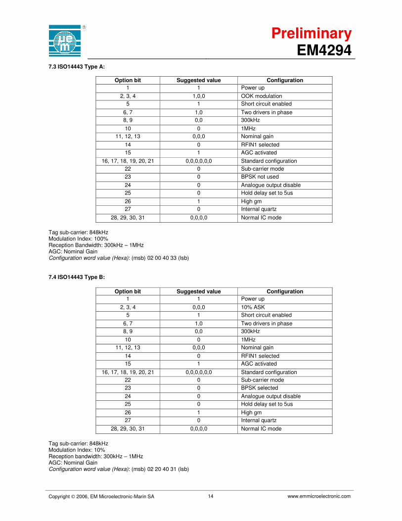
Example of Set Key Management password: INFO Resetting card ATR 3B 02 36 04 ; Default password for very first card INIT = 0xFF,0xFF,0xFF,0xFF; C-APDU 10 07 00 00 04 FF FF FF FF C-RPDU 90 00 ; Set New password phase 1, Example = 0x11, 0x22, 0x33, 0x44; C-APDU 10 08 00 00 04 11 22 33 44 C-RPDU 90 00 ; Set New password phase 2 (confirmation), C-APDU 10 08 01 01 04 11 22 33 44 C-RPDU 90 00 (RESET) ; Enter password to have access to key update function C-APDU 10 07 00 00 04 11 22 33 44 C-RPDU 90 00 Examples ok Key #7 write ; Write Key[7] = 0x12, 0xB1,0x1E, 0x0F, 0x18, 0x68, 0xAC, 0xF2, 0x27, 0x6B, 0x09, 0x87; C-APDU 10 06 07 00 0C 12 B1 1E 0F 18 68 AC F2 27 6B 09 87 C-RPDU 90 00 9.3 APDU Eddy Mutual Authentication Mutual authentication process is based on challenge/response process using EM proprietary algorithm.
The different steps are: 1) Reset EM4035 Crypto module 2) Send Key Selection command based on key number (0 to 255) 3) Send A1 : Challenge 4) Get f() response from EM4035 Crypto ModuleA2, 0x00, f(Key[sel], A1, A2) 5) Send g() to EM4035 Crypto module:
If (Authentication (g(),A1,A2,Key[Sel],f()) =1) Send (0x90, 0x00)
Else Send (0x90, 0xEE)
9.3.1 Select Authentication Key
CLA INS P1 P2 P3 SW1 SW2
0x10 0x01 Key
# 00 00
0x90 0x00
Note 1: case 0 APDU command no ACK INS performed Note 2: Key # range 0 to 255 9.3.2 Send A1 random number
CLA INS P1 P2 P3 DATA FIELD SW1 SW2
0x10 0x02 0x00 0x00 0x07 A1[0] A1[1] … A1[6]
0x90 0x00 9.3.3 Get A2 random number and f() function response
CLA INS P1 P2 P3 DATA FIELD SW1 SW2
0x10 0x03 0x00 0x00 0x0B
A2[0
] A2[1
] …
A2[6]
0x00 f[0] f[1] f[2] 0x90 0x00

Preliminary EM4294
Copyright 2006, EM Microelectronic-Marin SA 20 www.emmicroelectronic.com
9.3.4 Send g() function
CLA INS P1 P2 P3 DATA FIELD SW1 SW2
0x10 0x04 0x00 0x00 0x03 g[0] g[1] g[2]
0x90 AUTH
AUTH = 0x00 : successful mutual authentication AUTH = 0xEE : mutual authentication fail Note: the maximum of failing authentication is limited to 4 afterwards the device will never authenticate successfully. Example of Authentication sequence:
Let the initial value of key no. 7 contains: key[7][] =0x12, 0xB1, 0x1E, 0x0F, 0x18, 0x68, 0xAC, 0xF2, 0x27, 0x6B, 0x09, 0x87; and random value A12 equal A12[7] = 8E, 0x5D, 0x7D, 0x34, 0x24, 0x70, 0x23 Step 1(reset EM4294 card): EM4035 CRYPTO MODULE: 3B 02 36 04 Step 2 (select key): Key #7 uC : 10 01 07 00 00 ; No ACK INS with No data Case EM4035 CRYPTO MODULE : 90 00 Step 3 (send A1): uC : 10 02 00 00 07 EM4035 CRYPTO MODULE : 02 ; ACK INS with DataIn case uC : 8B 1D ED 24 24 37 BF ; A1 EM4035 CRYPTO MODULE :90 00 Step 4 (receive A2, dummy, f()): uC : 10 03 00 00 0B EM4035 CRYPTO MODULE Ack Ins : 03 ; ACK INS with DataOut case EM4035 CRYPTO MODULE DataOut : 8E 5D 7D 34 24 70 23 00 25 1A 8B ; A2, 0x00, f() EM4035 CRYPTO MODULESW : 90 00
Step 5 (send g()): uC : 10 04 00 00 03 ; EM4035 CRYPTO MODULE Ack Ins : 04 ; ACK INS with DataOut case EM4035 CRYPTO MODULE DataOut : 72 27 54 ; Send g() EM4035 CRYPTO MODULESW : 90 00 ; Authentication OK else 90 EE

Preliminary EM4294
Copyright 2006, EM Microelectronic-Marin SA 21 www.emmicroelectronic.com
9.4 Extended User Command Set
9.4.1 Get Chip Supplier Serial Number (CSSN)
CLA INS P1 P2 P3 DATA FIELD SW1 SW2 0x20 0x00 0x00 0x00 0x08
CSSN1
CSSN2
CSSN3
-------
-------
-------
-----
CSSN 8
0x90 0x00
Note: if P3!=8 this function will return 0x00 in data field
Note: CRC information not visible to User (system level information used to secure this data record) 9.4.2 Get Random number
CLA INS P1 P2 P3 DATA FIELD SW1 SW2
0x20 0x01 0x00 0x00 n
RNG
1 RNG
2 RNG
3 ------
- ------
- ------
- -----
RNG n
0x90 0x00
Note: if P3 > 0x10 this function will return 0x00 in data field 9.4.3 System Commands CLA INS P1 P2 P3 SW1 SW2
0x20 0x03 Sys Cmd
0x00 0x00
0x90 0x00
SysCmd : 0x01 : Go in Power Down State (to reduce power consumption) Note: To reduce further power Vcc could be switched off.

Preliminary EM4294
Copyright 2006, EM Microelectronic-Marin SA 22 www.emmicroelectronic.com
9.4.4 Read User Memory (EEPROM)
CLA INS P1 P2 P3 DATA FIELD SW1 SW2
0x20 0x10 Addr
L Addr
H n
Data
1 Data
2 Data
3 ------
- ------
- ------
- -----
Data n
0x90 0x00
Note: if P3 > 0x10 or if address specified is out of range this function will return 0x00 in data field 9.4.5 Write User Memory (EEPROM)
CLA INS P1 P2 P3 DATA FIELD SW1 SW2
0x20 0x20 Addr
L Addr
H n
Data 1
Data 2
Data 3
-------
-------
-------
-----
Data n
0x90 0x00
Note: if P3 > 0x10 or if address specified is out of range this function will get data bytes however it will not launch any memory update operation. Note: no data anti-tearing management performed in case of aborted update User available address range: 0x0000 -0xAE7F # 43KB
9.5 Implementation
9.5.1 Memory Mapping
Code Space view
Rom: 1KB
Data Space view
Ram: 768 Bytes
1000H
0400H
0000H 0000H
FFFFHFFFFH
56KB
GP NVM
1000H
0C00H
0300H
Application
Code
NVMCLR
F000H F000H
SysParameters (1p) Back upBuffer (7p)
SysParameters (1p) Back upBuffer (7p)
0C00H
3000H
Authentication
Keys
User’s
EEPROM # 43KB
Passwords
Ratification Number
Power Up counter
9.5.2 Security level The high security level relies on: EM proprietary algorithm and its secure implementation on EM4035 CRYPTO MODULE platform. FIPS140-2 Random number generation Key Management protected by password with maximum of 3 trials EM4035 Crypto algorithm 9.6 Power Consumption indications EM4035 CRYPTO MODULE device is placed in idle mode each time a new byte or new APDU command is expected. Current consumption in idle mode is below 170uA In running mode, it will sink less than 10mA . (Once PowerDown command has been sent, the power consumption will be reduced below 100 uA.

Preliminary EM4294
Copyright 2006, EM Microelectronic-Marin SA 23 www.emmicroelectronic.com
10 . Antenna connection configurations 10.1 Single Output Driver (100mW)
OSCOUT
Antenna
C12100nF
C822pF
DOUT
VCC
13.56MHz
L1
1uH
C2
120pF
ANT1
VDD
CRYPTO
C722pF
VCC
RFIN1INTERFACE
DVDDA1
C1
150pF
C11100nF
RFIN2
C410pF
INTERFACE
EN
SPI
C9100nF
RST
DVSS
DIN
AGD
OSCIN
VCC
C547pF
C3470pF
VSS
I/O
DCLK
DOUT1
C101uF
CLK
C610nF
Note: In the above example, only one demodulation input (RFIN1) is used. RFIN2 is connected to analogue ground though a 10nF capacitor. 10.2 Double parallel output driver (option bit 6, 200mW)
VSS
C4390pF
OSCIN
RFIN1
Coaxial Cable
C12100nF
DCLK
DIN
INTERFACE
VCC
DVDDA2
C15
1nF
VCC
C17
C6
CRYPTO
VCC
L1
180nH
C822pF
I/O
13.56MHz
VDD
L2
220nH
C101uF
C722pF
AGD
OSCOUT
C21.2nF
C14100nF
C1
1nF
CLK
C11100nF
ANT1
EM4294
DOUT
RFIN2
EN
C3390pF
DVSS
SPI
C131uF
C9100nF
C16
C52.2nF
ANT2 DOUT1
VCC
DVDDA1
Antenna
INTERFACE
RST
Note: In the above example, the remote antenna is connected to the EM4294 reader chip through a 50 Ohms transmission line (coaxial cable). A matching impedance network is inserted between the EM4294 output drivers (ANT1-ANT2) and the coaxial cable. This network adapts the EM4294 output impedance to an output impedance of 50 Ohms. Also, the impedance network associated with the 2 demodulation inputs (RFIN1-RFIN2) permit to have an AM (amplitude modulation) and PM (Phase modulation) demodulation.
Preliminary EM4294
Copyright 2006, EM Microelectronic-Marin SA 24 www.emmicroelectronic.com
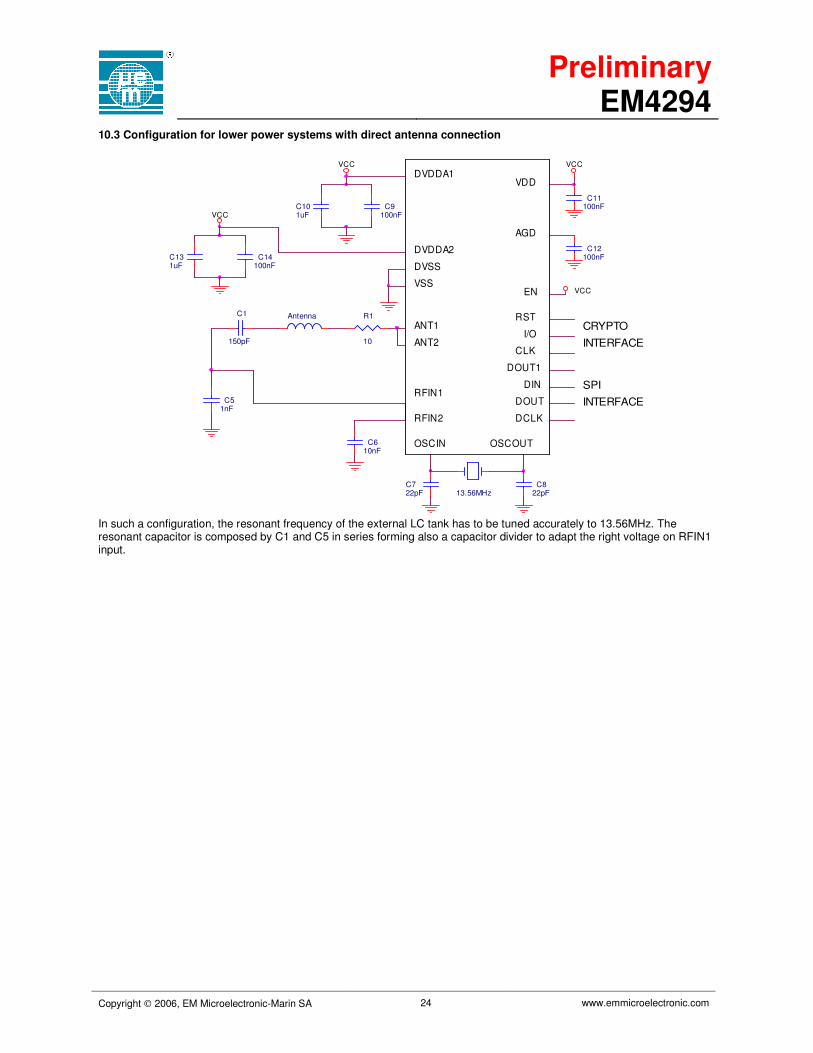
10.3 Configuration for lower power systems with direct antenna connection
RSTAntenna
CLK
C11100nF
AGD
VCC
C14100nF
SPI
DVDDA2
C722pF
C101uF
C12100nF
ANT2
C822pF
C1
150pF
C610nF
R1
10
VCC
DVDDA1
CRYPTO
13.56MHz
INTERFACE
VCC
DOUT
DCLK
OSCIN
DOUT1
RFIN2
EN
C9100nF
OSCOUT
INTERFACE
C131uF DVSS
VCC
VDD
C51nF
ANT1
VSS
RFIN1DIN
I/O
In such a configuration, the resonant frequency of the external LC tank has to be tuned accurately to 13.56MHz. The resonant capacitor is composed by C1 and C5 in series forming also a capacitor divider to adapt the right voltage on RFIN1 input.
Preliminary EM4294
Copyright 2006, EM Microelectronic-Marin SA 25 www.emmicroelectronic.com
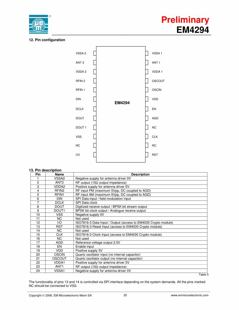
12. Pin configuration
13. Pin description
Pin Name Description
1 VSSA2 Negative supply for antenna driver 0V
2 ANT2 RF output (10Ω output impedance)
3 VDDA2 Positive supply for antenna driver 5V 4 RFIN2 RF input PM (maximum 5Vpp, DC coupled to AGD)
5 RFIN1 RF input AM (maximum 5Vpp, DC coupled to AGD)
6 DIN SPI Data input / field modulation input 7 DCLK SPI Data clock
8 DOUT Digitized receive output / BPSK bit stream output 9 DOUT1 BPSK bit clock output / Analogue receive output
10 VSS Negative supply 0V 11 NC Not used
12 I/O ISO7816-3 Data Input / Output (access to EM4035 Crypto module)
13 RST ISO7816-3 Reset Input (access to EM4035 Crypto module) 14 NC Not used
15 CLK ISO7816-3 Clock Input (access to EM4035 Crypto module) 16 NC Not used
17 AGD Reference voltage output 2.5V
18 EN Enable input
19 VDD Positive supply 5V
20 OSCIN Quartz oscillator input (no internal capacitor) 21 OSCOUT Quartz oscillator output (no internal capacitor)
22 VDDA1 Positive supply for antenna driver 5V 23 ANT1 RF output (10Ω output impedance)
24 VSSA1 Negative supply for antenna driver 0V Table 5
The functionality of pins 13 and 14 is controlled via SPI interface depending on the system demands. All the pins marked NC should be connected to VSS.
VSSA 2
ANT 2
VDDA 2
RFIN 2
RFIN 1
DIN
DCLK
DOUT
DOUT 1
VSS
NC
I/O
VSSA 1
ANT 1
VDDA 1
OSCOUT
OSCIN
VDD
EN
AGD
NC
CLK
NC
RST
EM4294

Preliminary EM4294
Copyright 2006, EM Microelectronic-Marin SA 26 www.emmicroelectronic.com
14. Package Information
15. Ordering Information
Part Number Package Delivery Form
EM4294SO24A SO24 Stick
16. Product Support Check our web site under Products/RF Identification section. Questions can be sent to [email protected].
EM Microelectronic-Marin SA (EM) makes no warranty for the use of its products, other than those expressly contained in the Company's standard warranty which is detailed in EM's General Terms of Sale located on the Company's web site. EM assumes no responsibility for any errors which may appear in this document, reserves the right to change devices or specifications detailed herein at any time without notice, and does not make any commitment to update the information contained herein. No licenses to patents or other intellectual property of EM are granted in connection with the sale of EM products, expressly or by implications. EM's products are not authorized for use as components in life support devices or systems.
© EM Microelectronic-Marin SA, 08/06 Rev. A