Embed Size (px)
Citation preview

Technical University of LodzDepartment of Microelectronics and Computer Science s
Electronic Technology Design and WorkshopElectronic Technology Design and Workshop IFE, B&T, V IFE, B&T, V semestersemester
Electronic Technology Design and Workshop
Presented and updated by
Przemek SekalskiDMCS room 2
2007

Technical University of LodzDepartment of Microelectronics and Computer Science s
Electronic Technology Design and WorkshopElectronic Technology Design and Workshop IFE, B&T, V IFE, B&T, V semestersemester
Electronic Technology Design and Workshop
Lecture 5
Microelectronics technology
Technical University of LodzDepartment of Microelectronics and Computer Science s
ElectronicElectronic TechnologyTechnology Design Design andand WorkshopWorkshop IFE, B&T, V IFE, B&T, V semestersemester 3
Acknowledgement
During preparation of this lecture many photos and descriptions was taken from various web pages.
To clarify the lecture I have not included all web addresses however I acknowledge the invaluable support

Technical University of LodzDepartment of Microelectronics and Computer Science s
ElectronicElectronic TechnologyTechnology Design Design andand WorkshopWorkshop IFE, B&T, V IFE, B&T, V semestersemester 4
CMOS Structure

Technical University of LodzDepartment of Microelectronics and Computer Science s
ElectronicElectronic TechnologyTechnology Design Design andand WorkshopWorkshop IFE, B&T, V IFE, B&T, V semestersemester 5
Silicon Integrated Circuits Technology
• Silicon wafer fabrication
• Silicon devices fabrication
• On-wafer testing
• Wafer-cutting
• Packaging
• Final testing

Technical University of LodzDepartment of Microelectronics and Computer Science s
ElectronicElectronic TechnologyTechnology Design Design andand WorkshopWorkshop IFE, B&T, V IFE, B&T, V semestersemester 6
Silicon wafer fabrication
• Monocrystalic silicon fabricating
• Cutting
• Mechanical and chemical polishing
Technical University of LodzDepartment of Microelectronics and Computer Science s
ElectronicElectronic TechnologyTechnology Design Design andand WorkshopWorkshop IFE, B&T, V IFE, B&T, V semestersemester 7
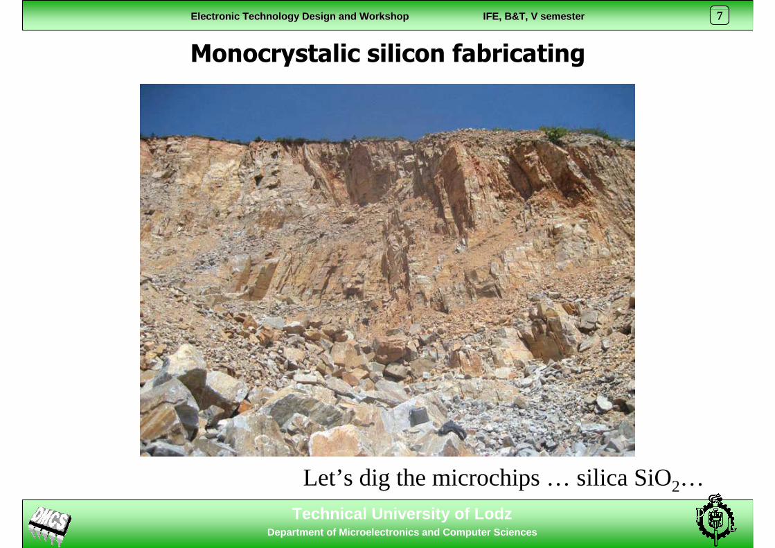
Monocrystalic silicon fabricating
Let’s dig the microchips … silica SiO2…

Technical University of LodzDepartment of Microelectronics and Computer Science s
ElectronicElectronic TechnologyTechnology Design Design andand WorkshopWorkshop IFE, B&T, V IFE, B&T, V semestersemester 8
Monocrystalic silicon fabricating
Pure silicon crystals are very rare (inclusions with gold and in volcanic exhalations).
Commonly silicon is found in the form of silicon dioxide SiO 2 (silica), and silicate.
Measured by mass, silicon makes up 26% of the Earth's crust.
It is, after oxygen, the second most abundant element on Earth.
Technical University of LodzDepartment of Microelectronics and Computer Science s
ElectronicElectronic TechnologyTechnology Design Design andand WorkshopWorkshop IFE, B&T, V IFE, B&T, V semestersemester 9
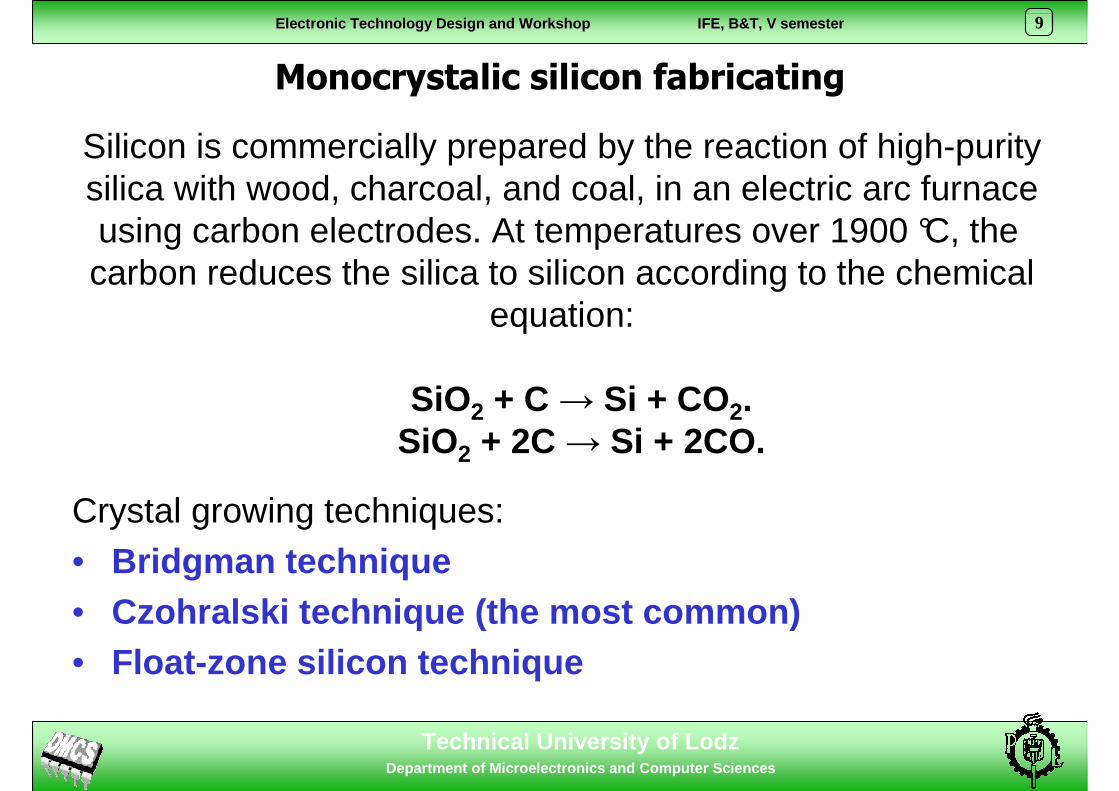
Monocrystalic silicon fabricating
Crystal growing techniques:• Bridgman technique• Czohralski technique (the most common)• Float-zone silicon technique
Silicon is commercially prepared by the reaction of high-purity silica with wood, charcoal, and coal, in an electric arc furnaceusing carbon electrodes. At temperatures over 1900 °C, the carbon reduces the silica to silicon according to the chemical
equation:
SiO2 + C → Si + CO2.SiO2 + 2C → Si + 2CO.

Technical University of LodzDepartment of Microelectronics and Computer Science s
ElectronicElectronic TechnologyTechnology Design Design andand WorkshopWorkshop IFE, B&T, V IFE, B&T, V semestersemester 10
Czohralski method
Silicon chunkswith silica
Molten silicon1600-1900 oC
Si melting point 1414 oC
Silicon ingot creation
Seed silicon monocrystalinsertion
Dopant impurity atoms such as
boron or phosphorus are added to
the molten intrinsic silicon to create
the n-type or p-type extrinsic silicon
Whole process is done in the inert atmosphere, such as argon

Technical University of LodzDepartment of Microelectronics and Computer Science s
ElectronicElectronic TechnologyTechnology Design Design andand WorkshopWorkshop IFE, B&T, V IFE, B&T, V semestersemester 11
Czohralski method
The process is named after
Polish scientist Jan
Czochralski, who
discovered the method in
1916 while investigating the
crystallization rates of metals
The ingots might be up to 1 to 2
metres long and the diameter is
around 200 mm and 300 mm.
The largest silicon ingots
produced today are 400 mm
in diameter.
Technical University of LodzDepartment of Microelectronics and Computer Science s
ElectronicElectronic TechnologyTechnology Design Design andand WorkshopWorkshop IFE, B&T, V IFE, B&T, V semestersemester 12
Monocrystalic silicon fabricating
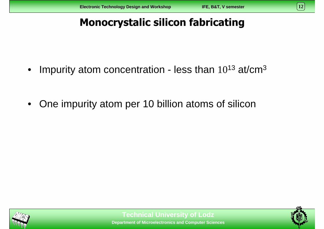
• Impurity atom concentration - less than 1013 at/cm3
• One impurity atom per 10 billion atoms of silicon

Technical University of LodzDepartment of Microelectronics and Computer Science s
ElectronicElectronic TechnologyTechnology Design Design andand WorkshopWorkshop IFE, B&T, V IFE, B&T, V semestersemester 13
Monocrystal cutting
Silicon Ingot
Diamond saw
Stainless steel Silicon wafer
The ingot is cut into the wafer using the diamond saw.(slices thickness around 0,5-1mm).
The wafer surface has many crystal net damages.Mechanical and chemical polishing is needed.
Technical University of LodzDepartment of Microelectronics and Computer Science s
ElectronicElectronic TechnologyTechnology Design Design andand WorkshopWorkshop IFE, B&T, V IFE, B&T, V semestersemester 14
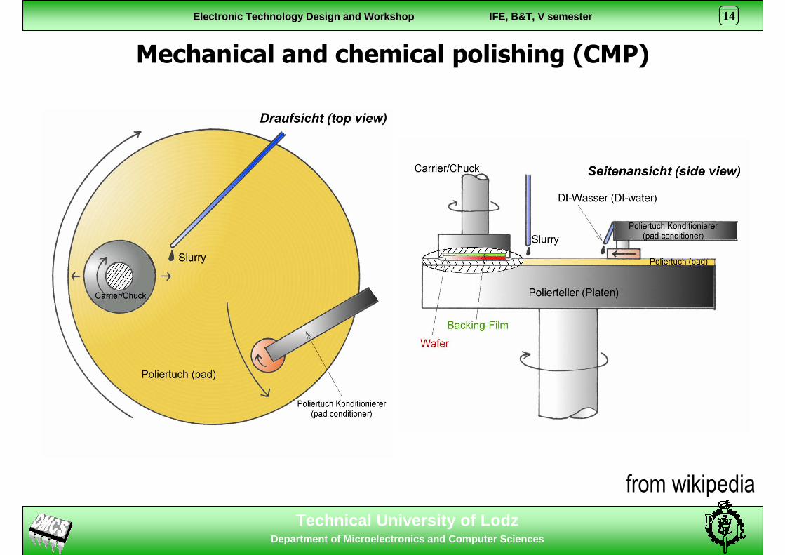
Mechanical and chemical polishing (CMP)
from wikipedia

Technical University of LodzDepartment of Microelectronics and Computer Science s
ElectronicElectronic TechnologyTechnology Design Design andand WorkshopWorkshop IFE, B&T, V IFE, B&T, V semestersemester 15
Crystal orientation markers
N-type
P-type
<100>
<100>
<111>
<111>
<110>

Technical University of LodzDepartment of Microelectronics and Computer Science s
ElectronicElectronic TechnologyTechnology Design Design andand WorkshopWorkshop IFE, B&T, V IFE, B&T, V semestersemester 16
Some crystallography
Silicon crystal seen along
the <110> direction
Silicon crystal seen along
the <100> direction.

Technical University of LodzDepartment of Microelectronics and Computer Science s
ElectronicElectronic TechnologyTechnology Design Design andand WorkshopWorkshop IFE, B&T, V IFE, B&T, V semestersemester 17
Till now we have …wafers

Technical University of LodzDepartment of Microelectronics and Computer Science s
ElectronicElectronic TechnologyTechnology Design Design andand WorkshopWorkshop IFE, B&T, V IFE, B&T, V semestersemester 18
Technology Process Stepsinitial oxide
first nitride deposition
NTUB mask
well etch (nitride)
NTUB implant
well oxidation
self aligned P-well implant
well drive-in
pad oxide
second nitride deposition
active area mask
active area etch (nitride)
N-field mask
N-field implant
field oxide
sacrificial oxide
Vt adjust implant
gate oxide
poly1 deposition
high-resistive implant
high-resistive mask
poly1 doping
capacitor oxide
poly2 deposition
poly2 doping
poly2 mask
poly2 etch
poly1 mask
poly1 etch
N-LDD mask
N-LDD implant
P-LDD implant
spacer formation
N+ implant mask
N+ implant
P+ implant mask
P+ implant
S/D anneal
BPSG deposition/reflow
contact mask
contact etch
plug implant mask
plug implant / anneal
barrier deposition
metal1 deposition
metal1 mask
metal1 etch
IMD / planarisation
via mask
via etch
metal2 deposition
metal2 mask
metal2 etch
passivation deposition
pad mask
pad etch
alloy
back side grinding

Technical University of LodzDepartment of Microelectronics and Computer Science s
ElectronicElectronic TechnologyTechnology Design Design andand WorkshopWorkshop IFE, B&T, V IFE, B&T, V semestersemester 19
Silicon devices and interconnection fabrication
• Changing characteristic of material or new layer applying (deposition)
• (Photo) lithography
• Etching
Technical University of LodzDepartment of Microelectronics and Computer Science s
ElectronicElectronic TechnologyTechnology Design Design andand WorkshopWorkshop IFE, B&T, V IFE, B&T, V semestersemester 20
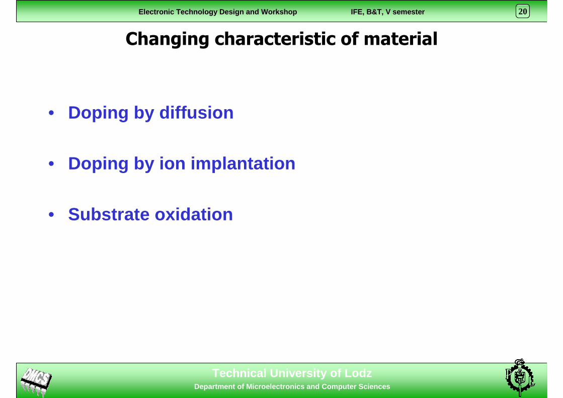
Changing characteristic of material
• Doping by diffusion
• Doping by ion implantation
• Substrate oxidation

Technical University of LodzDepartment of Microelectronics and Computer Science s
ElectronicElectronic TechnologyTechnology Design Design andand WorkshopWorkshop IFE, B&T, V IFE, B&T, V semestersemester 21
Diffusion
• Temperature 800 - 1200°C• Boron, phosphor or arsenic atoms tend to penetrate the
silicon• Impurity atoms introduced by implantation, deposition, or
epitaxy then diffuse during any high temperature steps in an IC process
Physical phenomenon where particles such as impurity atoms in a semiconductor tend to flow from high
concentration to low concentration
Technical University of LodzDepartment of Microelectronics and Computer Science s
ElectronicElectronic TechnologyTechnology Design Design andand WorkshopWorkshop IFE, B&T, V IFE, B&T, V semestersemester 22
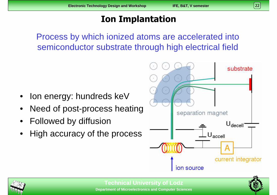
Ion Implantation
• Ion energy: hundreds keV• Need of post-process heating• Followed by diffusion• High accuracy of the process
Process by which ionized atoms are accelerated into semiconductor substrate through high electrical field

Technical University of LodzDepartment of Microelectronics and Computer Science s
ElectronicElectronic TechnologyTechnology Design Design andand WorkshopWorkshop IFE, B&T, V IFE, B&T, V semestersemester 23
Substrate Oxidation
utlenianie termiczne w parze wodnejtlenki polowe300 - 1000
utlenianie termiczne w parze wodnej
lub CVD
tlenki maskujące oraz
pasywujące powierzchnię200 - 500
utlenianie termiczne w suchym tlenietlenki "podkładowe" w technologii LOCOS
20 - 50
utlenianie termiczne w suchym tlenietlenki bramkowe
oraz kondensatorowe15 - 50
utlenianie termiczne w suchym tlenietlenki tunelowe2 - 6
Podstawowa metoda wytwarzaniaZastosowanie warstwyGrubość tlenku [nm]

Technical University of LodzDepartment of Microelectronics and Computer Science s
ElectronicElectronic TechnologyTechnology Design Design andand WorkshopWorkshop IFE, B&T, V IFE, B&T, V semestersemester 24
Process where a layer of silicon dioxide is thermally grown on a silicon wafer
At elevated temperature, a gas containing oxygen or a water vapor flows through a furnace and onto a silicon surface causing a chemical reaction
Substrate Oxidation

Technical University of LodzDepartment of Microelectronics and Computer Science s
ElectronicElectronic TechnologyTechnology Design Design andand WorkshopWorkshop IFE, B&T, V IFE, B&T, V semestersemester 25
• Temperature 950 - 1150°C• In the growth of the oxide, the thickness of the silicon
layer is consumed by 45%• Speed depends on temperature and pressure• Dry or wet:
222
22
22 HSiOOHSi
SiOOSi
+→+→+
Substrate Oxidation

Technical University of LodzDepartment of Microelectronics and Computer Science s
ElectronicElectronic TechnologyTechnology Design Design andand WorkshopWorkshop IFE, B&T, V IFE, B&T, V semestersemester 26
New layer deposition
Epitaxy (homo)The growth of a single crystal semiconductor film on a
single crystal substrate of the same semiconductor
Epitaxy (hetero)The growth of semiconductor layers on substrates of
different types

Technical University of LodzDepartment of Microelectronics and Computer Science s
ElectronicElectronic TechnologyTechnology Design Design andand WorkshopWorkshop IFE, B&T, V IFE, B&T, V semestersemester 27
• Chemical Vapour Deposition (CVD)– Low Pressure CVD (LPCVD)– Plasma Enhanced CVD (PECVD)– Ultrahigh vacuum CVD (UHVCVD)– And plenty others…
• Physical Vapour Deposition (PVD)– Evaporative deposition– Electron Beam Physical Vapor Deposition – Sputter deposition – Cathodic Arc Deposition – Pulsed laser deposition
New layer deposition

Technical University of LodzDepartment of Microelectronics and Computer Science s
ElectronicElectronic TechnologyTechnology Design Design andand WorkshopWorkshop IFE, B&T, V IFE, B&T, V semestersemester 28
• Polycrystalic silicon - epitaxy950 - 1250 °C
• Silicon nitride300 °C PECVD, 700 °C LPCVD
• Silicon dioxide450-600 °C
Chemical Vapour Deposition
HClSiHSiCl
HClSisilanSiHSiCl
42
42)(
24
44
+→++→+
24334 124)(3 HNSiNHsilanSiH +→+
2224 2)( HSiOOsilanSiH +→+

Technical University of LodzDepartment of Microelectronics and Computer Science s
ElectronicElectronic TechnologyTechnology Design Design andand WorkshopWorkshop IFE, B&T, V IFE, B&T, V semestersemester 29
Physical Vapour Deposition
• Thin film technology
• Evaporation or ion bombing (sputtering)
• Metalisation

Technical University of LodzDepartment of Microelectronics and Computer Science s
ElectronicElectronic TechnologyTechnology Design Design andand WorkshopWorkshop IFE, B&T, V IFE, B&T, V semestersemester 30
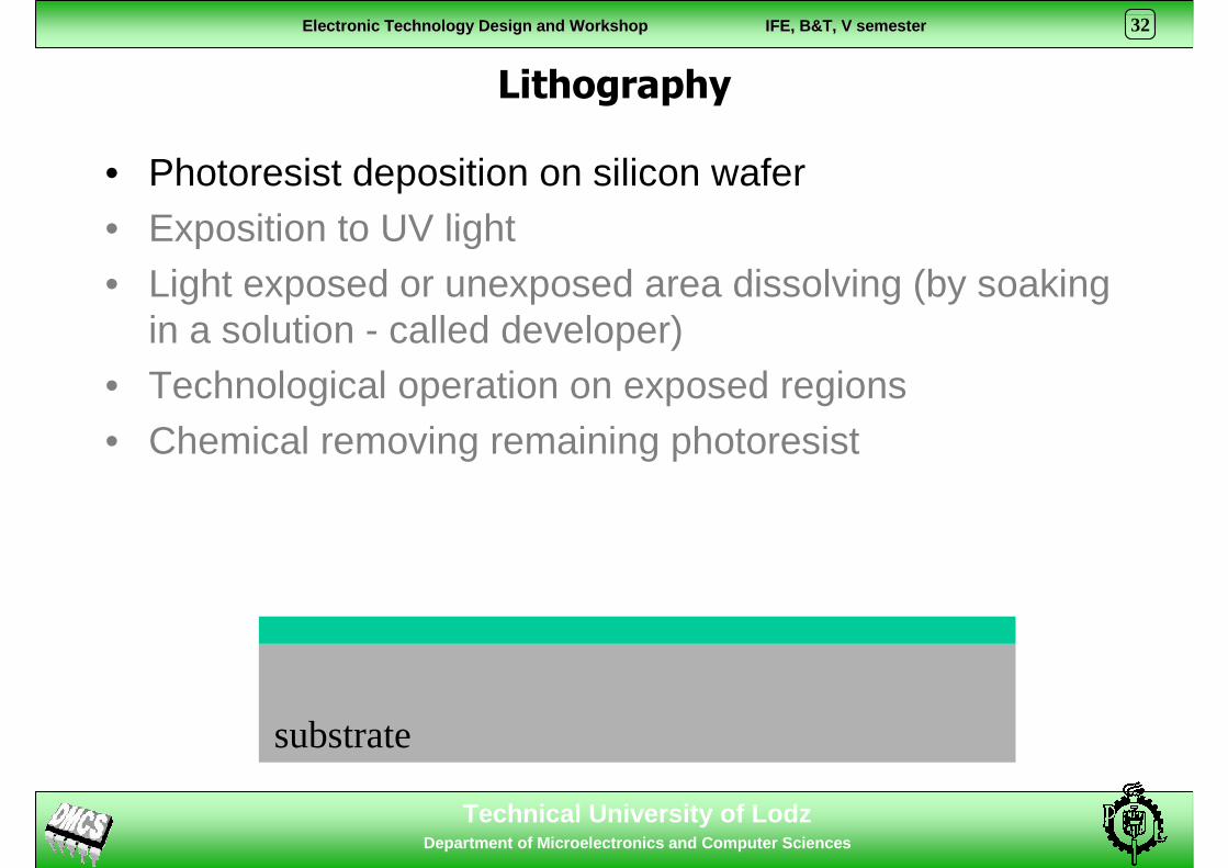
Lithography
• Photoresist deposition on silicon wafer• Exposition to UV light• Light exposed or unexposed area dissolving (by soaking
in a solution - called developer)• Technological operation on exposed regions• Chemical removing remaining photoresist

Technical University of LodzDepartment of Microelectronics and Computer Science s
ElectronicElectronic TechnologyTechnology Design Design andand WorkshopWorkshop IFE, B&T, V IFE, B&T, V semestersemester 31
Lithography
substrate
• Photoresist deposition on silicon wafer• Exposition to UV light• Light exposed or unexposed area dissolving (by soaking
in a solution - called developer)• Technological operation on exposed regions• Chemical removing remaining photoresist
substrate
Technical University of LodzDepartment of Microelectronics and Computer Science s
ElectronicElectronic TechnologyTechnology Design Design andand WorkshopWorkshop IFE, B&T, V IFE, B&T, V semestersemester 32
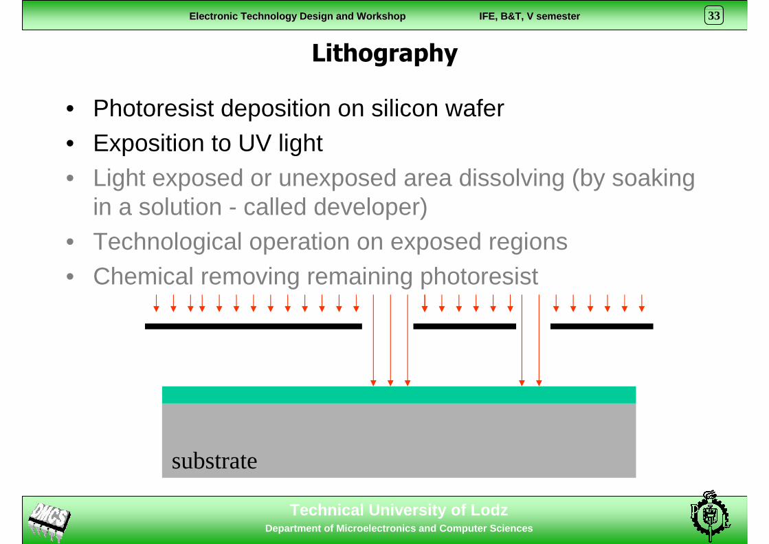
Lithography
• Photoresist deposition on silicon wafer• Exposition to UV light• Light exposed or unexposed area dissolving (by soaking
in a solution - called developer)• Technological operation on exposed regions• Chemical removing remaining photoresist
substrate
Technical University of LodzDepartment of Microelectronics and Computer Science s
ElectronicElectronic TechnologyTechnology Design Design andand WorkshopWorkshop IFE, B&T, V IFE, B&T, V semestersemester 33
Lithography
substrate
• Photoresist deposition on silicon wafer• Exposition to UV light• Light exposed or unexposed area dissolving (by soaking
in a solution - called developer)• Technological operation on exposed regions• Chemical removing remaining photoresist

Technical University of LodzDepartment of Microelectronics and Computer Science s
ElectronicElectronic TechnologyTechnology Design Design andand WorkshopWorkshop IFE, B&T, V IFE, B&T, V semestersemester 34
Lithography
substrate
• Photoresist deposition on silicon wafer• Exposition to UV light• Light exposed or unexposed area dissolving (by soaking
in a solution - called developer)• Technological operation on exposed regions• Chemical removing remaining photoresist
Mask

Technical University of LodzDepartment of Microelectronics and Computer Science s
ElectronicElectronic TechnologyTechnology Design Design andand WorkshopWorkshop IFE, B&T, V IFE, B&T, V semestersemester 35
Lithography
substrate
• Photoresist deposition on silicon wafer• Exposition to UV light• Light exposed or unexposed area dissolving (by soaking
in a solution - called developer)• Technological operation on exposed regions• Chemical removing remaining photoresist
Technical University of LodzDepartment of Microelectronics and Computer Science s
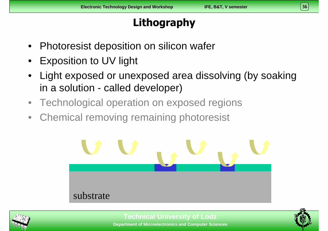
ElectronicElectronic TechnologyTechnology Design Design andand WorkshopWorkshop IFE, B&T, V IFE, B&T, V semestersemester 36
Lithography
substrate
• Photoresist deposition on silicon wafer• Exposition to UV light• Light exposed or unexposed area dissolving (by soaking
in a solution - called developer)• Technological operation on exposed regions• Chemical removing remaining photoresist

Technical University of LodzDepartment of Microelectronics and Computer Science s
ElectronicElectronic TechnologyTechnology Design Design andand WorkshopWorkshop IFE, B&T, V IFE, B&T, V semestersemester 37
Lithography
substrate
• Photoresist deposition on silicon wafer• Exposition to UV light• Light exposed or unexposed area dissolving (by soaking
in a solution - called developer)• Technological operation on exposed regions• Chemical removing remaining photoresist

Technical University of LodzDepartment of Microelectronics and Computer Science s
ElectronicElectronic TechnologyTechnology Design Design andand WorkshopWorkshop IFE, B&T, V IFE, B&T, V semestersemester 38
Lithography
substrate
• Photoresist deposition on silicon wafer• Exposition to UV light• Light exposed or unexposed area dissolving (by soaking
in a solution - called developer)• Technological operation on exposed regions• Chemical removing remaining photoresist
i.e. ion deposition

Technical University of LodzDepartment of Microelectronics and Computer Science s
ElectronicElectronic TechnologyTechnology Design Design andand WorkshopWorkshop IFE, B&T, V IFE, B&T, V semestersemester 39
Lithography
substrate
• Photoresist deposition on silicon wafer• Exposition to UV light• Light exposed or unexposed area dissolving (by soaking
in a solution - called developer)• Technological operation on exposed regions• Chemical removing remaining photoresist
i.e. ion deposition and heating (diffusion)

Technical University of LodzDepartment of Microelectronics and Computer Science s
ElectronicElectronic TechnologyTechnology Design Design andand WorkshopWorkshop IFE, B&T, V IFE, B&T, V semestersemester 40
Lithography
substrate
• Photoresist deposition on silicon wafer• Exposition to UV light• Light exposed or unexposed area dissolving (by soaking
in a solution - called developer)• Technological operation on exposed regions• Chemical removing remaining photoresist
i.e. ion deposition and heating (diffusion)

Technical University of LodzDepartment of Microelectronics and Computer Science s
ElectronicElectronic TechnologyTechnology Design Design andand WorkshopWorkshop IFE, B&T, V IFE, B&T, V semestersemester 41
Lithography
substrate
• Photoresist deposition on silicon wafer• Exposition to UV light• Light exposed or unexposed area dissolving (by soaking
in a solution - called developer)• Technological operation on exposed regions• Chemical removing remaining photoresist
i.e. ion deposition and heating (diffusion)

Technical University of LodzDepartment of Microelectronics and Computer Science s
ElectronicElectronic TechnologyTechnology Design Design andand WorkshopWorkshop IFE, B&T, V IFE, B&T, V semestersemester 42
Lithography
substrate
• Thin silicon dioxide deposition

Technical University of LodzDepartment of Microelectronics and Computer Science s
ElectronicElectronic TechnologyTechnology Design Design andand WorkshopWorkshop IFE, B&T, V IFE, B&T, V semestersemester 43
Lithography
substrate
• Photoresist deposition and exposition to UV

Technical University of LodzDepartment of Microelectronics and Computer Science s
ElectronicElectronic TechnologyTechnology Design Design andand WorkshopWorkshop IFE, B&T, V IFE, B&T, V semestersemester 44
Lithography
substrate
• Etching
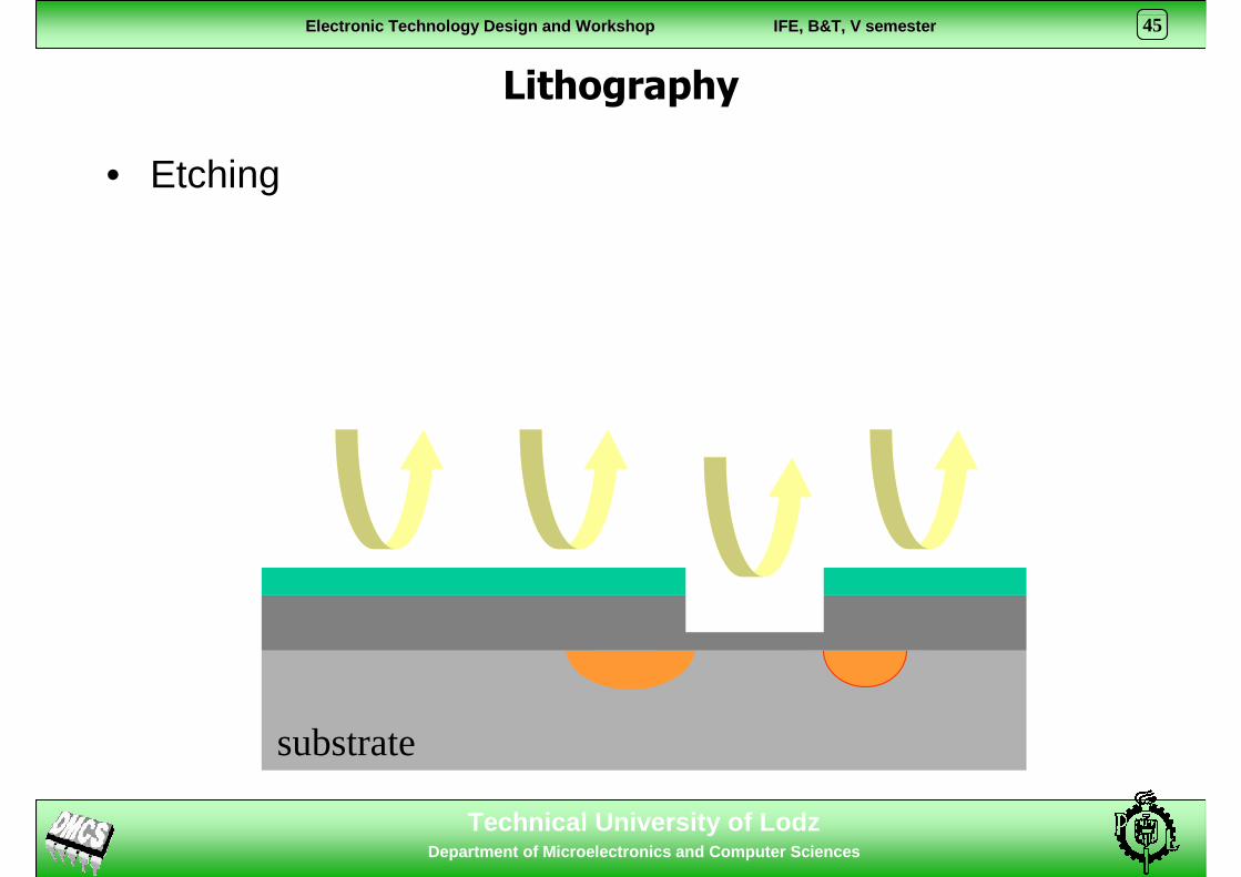
Technical University of LodzDepartment of Microelectronics and Computer Science s
ElectronicElectronic TechnologyTechnology Design Design andand WorkshopWorkshop IFE, B&T, V IFE, B&T, V semestersemester 45
Lithography
substrate
• Etching

Technical University of LodzDepartment of Microelectronics and Computer Science s
ElectronicElectronic TechnologyTechnology Design Design andand WorkshopWorkshop IFE, B&T, V IFE, B&T, V semestersemester 46
Lithography
substrate
• Polysilicon deposition

Technical University of LodzDepartment of Microelectronics and Computer Science s
ElectronicElectronic TechnologyTechnology Design Design andand WorkshopWorkshop IFE, B&T, V IFE, B&T, V semestersemester 47
Lithography
substrate
• Photoresist removal
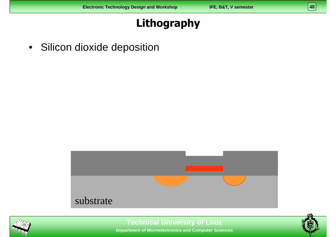
Technical University of LodzDepartment of Microelectronics and Computer Science s
ElectronicElectronic TechnologyTechnology Design Design andand WorkshopWorkshop IFE, B&T, V IFE, B&T, V semestersemester 48
Lithography
substrate
• Silicon dioxide deposition
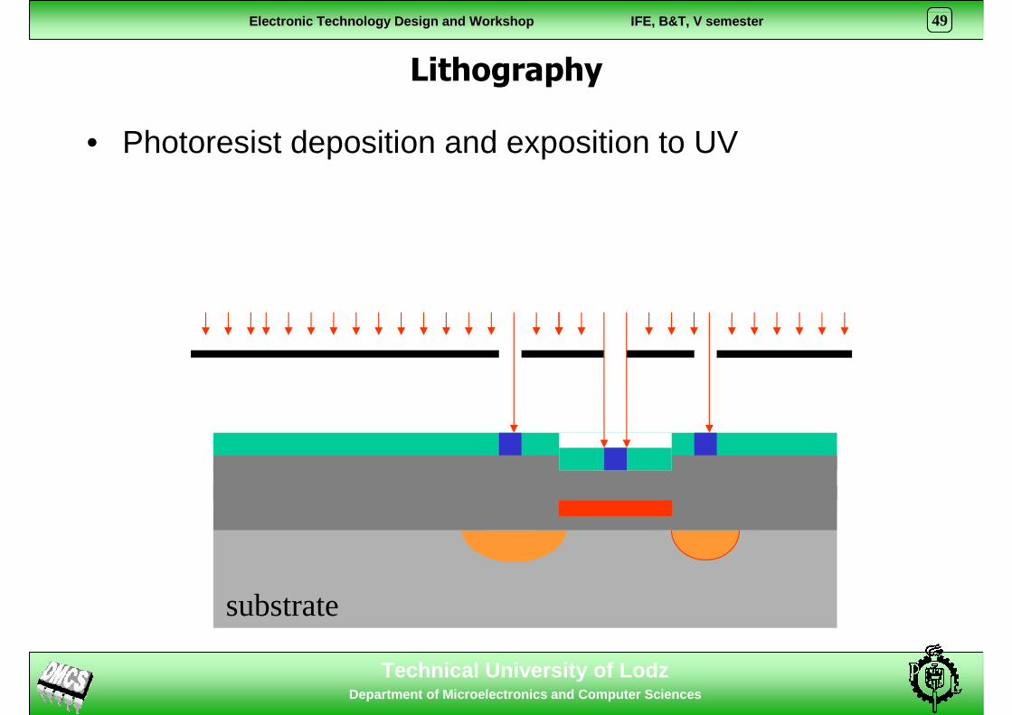
Technical University of LodzDepartment of Microelectronics and Computer Science s
ElectronicElectronic TechnologyTechnology Design Design andand WorkshopWorkshop IFE, B&T, V IFE, B&T, V semestersemester 49
Lithography
substrate
• Photoresist deposition and exposition to UV

Technical University of LodzDepartment of Microelectronics and Computer Science s
ElectronicElectronic TechnologyTechnology Design Design andand WorkshopWorkshop IFE, B&T, V IFE, B&T, V semestersemester 50
Lithography
substrate
• Etching

Technical University of LodzDepartment of Microelectronics and Computer Science s
ElectronicElectronic TechnologyTechnology Design Design andand WorkshopWorkshop IFE, B&T, V IFE, B&T, V semestersemester 51
Lithography
substrate
• Metalisation
Technical University of LodzDepartment of Microelectronics and Computer Science s
ElectronicElectronic TechnologyTechnology Design Design andand WorkshopWorkshop IFE, B&T, V IFE, B&T, V semestersemester 52
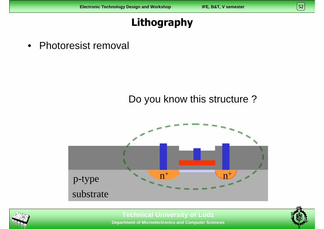
Lithography
substrate
• Photoresist removal
Do you know this structure ?
p-type n+ n+

Technical University of LodzDepartment of Microelectronics and Computer Science s
ElectronicElectronic TechnologyTechnology Design Design andand WorkshopWorkshop IFE, B&T, V IFE, B&T, V semestersemester 53
Exposing methods
• Whole-wafer projection lithography
• contact printing
• direct step-on-wafer (multiply wafer exposition)

Technical University of LodzDepartment of Microelectronics and Computer Science s
ElectronicElectronic TechnologyTechnology Design Design andand WorkshopWorkshop IFE, B&T, V IFE, B&T, V semestersemester 54
Lithography types
• Optical (mostly UV)• Roentgen• Electron• Ion
The wavelength determine the mask precision (diffraction phenomenon)
Technical University of LodzDepartment of Microelectronics and Computer Science s
ElectronicElectronic TechnologyTechnology Design Design andand WorkshopWorkshop IFE, B&T, V IFE, B&T, V semestersemester 55
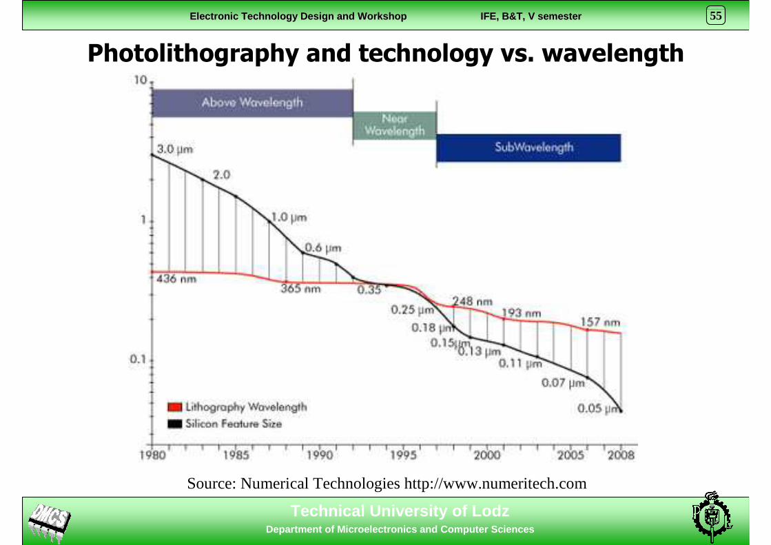
Source: Numerical Technologies http://www.numeritech.com
Photolithography and technology vs. wavelength

Technical University of LodzDepartment of Microelectronics and Computer Science s
ElectronicElectronic TechnologyTechnology Design Design andand WorkshopWorkshop IFE, B&T, V IFE, B&T, V semestersemester 56
Source: Numerical Technologies http://www.numeritech.com
Optical Proximity Correction

Technical University of LodzDepartment of Microelectronics and Computer Science s
ElectronicElectronic TechnologyTechnology Design Design andand WorkshopWorkshop IFE, B&T, V IFE, B&T, V semestersemester 57
Phase-Shifting Masks
Source: Numerical Technologies http://www.numeritech.com

Technical University of LodzDepartment of Microelectronics and Computer Science s
ElectronicElectronic TechnologyTechnology Design Design andand WorkshopWorkshop IFE, B&T, V IFE, B&T, V semestersemester 58
Photo-resist patterns printed by lithography must be transferred onto layers that comprise the integrated circuit
A common process is to selectively etch away the layer material no covered by resist.
The etching process can be used to etch contacts holes in an oxide layer or etch most polysilicon materials away to leave narrow islands for MOSFET gates
Etching

Technical University of LodzDepartment of Microelectronics and Computer Science s
ElectronicElectronic TechnologyTechnology Design Design andand WorkshopWorkshop IFE, B&T, V IFE, B&T, V semestersemester 59
• Wet and dry• Dry etching
– physical (i.e. sputtering: high accelerated ions bombard the etched material)
– chemical (etching compound)– mixed– photochemical
• Dry etching method advantages:– Selectivity - high resolution– High anisotropy
Etching

Technical University of LodzDepartment of Microelectronics and Computer Science s
ElectronicElectronic TechnologyTechnology Design Design andand WorkshopWorkshop IFE, B&T, V IFE, B&T, V semestersemester 60
Lithography, deposition, implantation, etching
And finally the wafer with many devices on board

Technical University of LodzDepartment of Microelectronics and Computer Science s
ElectronicElectronic TechnologyTechnology Design Design andand WorkshopWorkshop IFE, B&T, V IFE, B&T, V semestersemester 61
On-wafer testing

Technical University of LodzDepartment of Microelectronics and Computer Science s
ElectronicElectronic TechnologyTechnology Design Design andand WorkshopWorkshop IFE, B&T, V IFE, B&T, V semestersemester 62
Dicing
dies
Technical University of LodzDepartment of Microelectronics and Computer Science s
ElectronicElectronic TechnologyTechnology Design Design andand WorkshopWorkshop IFE, B&T, V IFE, B&T, V semestersemester 63
Dice packaging

Technical University of LodzDepartment of Microelectronics and Computer Science s
ElectronicElectronic TechnologyTechnology Design Design andand WorkshopWorkshop IFE, B&T, V IFE, B&T, V semestersemester 64
Packaging

Technical University of LodzDepartment of Microelectronics and Computer Science s
ElectronicElectronic TechnologyTechnology Design Design andand WorkshopWorkshop IFE, B&T, V IFE, B&T, V semestersemester 65
Technical University of LodzDepartment of Microelectronics and Computer Science s
ElectronicElectronic TechnologyTechnology Design Design andand WorkshopWorkshop IFE, B&T, V IFE, B&T, V semestersemester 66
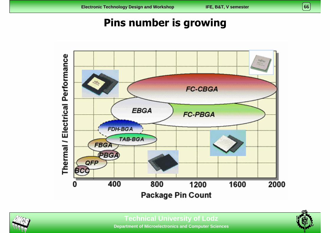
Pins number is growing

Technical University of LodzDepartment of Microelectronics and Computer Science s
ElectronicElectronic TechnologyTechnology Design Design andand WorkshopWorkshop IFE, B&T, V IFE, B&T, V semestersemester 67
Technical University of LodzDepartment of Microelectronics and Computer Science s
ElectronicElectronic TechnologyTechnology Design Design andand WorkshopWorkshop IFE, B&T, V IFE, B&T, V semestersemester 68
Next lectureMore complex devices : MUX, flip-flops
Thank you for your attention