Embed Size (px)
Citation preview
Electronic Systems
Lab Report
Andrew DiluciaA10938

Contents
Introduction…………………………………………………………………………………p2
Part 1
Inverting Op Amp……………………………………...…………………………………….p3
Inverting Buffer………………………………………...…………………………………….p7
Non-Inverting Amplifier………………………..……...…………………………………….p9
Non-Inverting Buffer…………………………………...……………………..…………….p14
Low Pass Filter………………………………………...……………………...…………….p15
High Pass Filter……………………...………………...……………………...…………….p18
Band Pass Filter………………………...……………...……………………...…………….p20
Butterworth Filter………………………...……….…...……………………...…………….p23
Chebyshev Filter……………………….....…………...……………………...…………….p27
Integration Amplifier…………………...……………...……………………...…………….p30
Differentiator Amplifier………………..……………...……………………...…………….p32
Balanced Line Driver………………………...…...…...……………………...…………….p34
Part 2
Blood Pressure Monitor…………………………..………………………………………...p40
Part 3
Simple AM Receiver……….….…………………………………………..………………..p43
Part 4
Switched Mode Power Supply (Flyback Converter)……..…………...…………………….p47
Part 5
PID Controller………………………………………………………...…………………….p49
Part 6
Music Circuit…………………………...……………...……………………...…………….p55
Part 7
Code Generation………………...……...……………...……………………...…………….p59
Conclusion………………………………………………………………………………….p64
References………………………………………………………………………………….p65
1

Introduction
Electronic systems can be found all around us in everyday life, like for example in a stereo system or a blood pressure monitor. They can be defined as the interconnection of parts or components that processes information that has been inputted from various devices such as sensors or computers to various types of outputs by electronic means.
For this report I was tasked with the investigation of various aspects of electronic systems mainly revolving around op amps. Throughout the semester I simulated and tested various systems to verify the outputs and recorded the results to analyse the data collected, to confirm the circuit was working as expected. These investigations involved building various electronic systems within Scilab/XCOS, which is a piece of simulation software to test the circuit. I also used Multisim to try simulate some models that I could not get working in Scilab.
The investigations contained seven parts and they are;
Various Op Amp Circuits
Blood Pressure Monitor
Simple AM Receiver
Switch Mode Power Supply
PID Controller
Music Circuit
Code Generation
This report was created to document the various stages of my investigations and were carried out by simulating the various systems in the lab on a PC or on my laptop.
2
Part 1
For this part of my investigations I was tasked with modelling variations of the op-amp circuit.
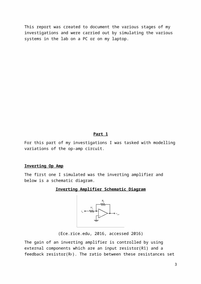
Inverting Op Amp
The first one I simulated was the inverting amplifier and below is a schematic diagram.
Inverting Amplifier Schematic Diagram
(Ece.rice.edu, 2016, accessed 2016)
The gain of an inverting amplifier is controlled by using external components which are an input resistor(R1) and a feedback resistor(RF). The ratio between these resistances set the gain. Also the point where the input and feedback resistors meet is known as a virtual earth and can be thought of as 0 Volts. The input is connected to the inverting input on the op-amp therefore the output would be inverted too. We can calculate the gain with the following formula;
(R F)(R1)
=−Gain(A)
As we can see from the formula the feedback resistor divided by the input resistor gives the gain but it is a negative number and this is because it is inverted. I built the model for the inverting amplifier in XCOS with a gain of 100 and can be seen below;
Inverting Amplifier XCOS Model (100 gain)
3

As we can see from the picture of the model on the previous page the input resistor was set to 1KΩ (highlighted in blue) and the feedback resistor was set to 100KΩ (highlighted in red). So when I use the formula from the previous page I could calculate what the expected output should be.
−(R F)(R1)
=Gain(A)
−1000001000
=−100
Gain=−100
To prove that the gain should be 100, I first altered the final integration time to 1.0E-6 and this is the overall run time for the simulation as seen below
XCOS Model Parameters
I then ran the simulation in XCOS and below are the scope results for a gain of 100.
Inverting Amplifier Scope Results (100 gain)
4

As we can see from the scope results on the previous page, when a 1V, 100KHz signal was injected into the circuit the output is 100 times greater than the input. This proved that the ratio between these two resistors controls the gain.
I then altered the feedback resistor to 50KΩ to alter the gain down from 100 to 50 and this can be seen below.
Inverting Amplifier XCOS Model (50 gain)
I then ran the simulation and below are the scope results.
Inverting Amplifier Scope Results (50 gain)
5

As we can see from the scope results on the previous page, when a 1V, 100KHz signal was injected into the circuit the output is now 50 times greater than the input. This proves that the ratio between these two resistors controls the gain.
Next I tried setting the resistance of both to the same value and this would give a gain of 1. This can be seen on the next page.
Inverting Amplifier XCOS Model (1 gain)
I then ran the simulation and below are the scope results.
Inverting Amplifier Scope Results (1 gain)
As we can see from the scope results when a 1V, 100KHz signal was injected into the circuit the output was the same as the input. This proved that the ratio between these two resistors once again controls the gain. Therefore, we can see the inverting amplifier uses negative feedback to accurately control the overall gain of the amplifier.
6

Inverting Buffer
Next I simulated an inverting buffer and this circuit is exactly the same as an inverting amplifier. The inverting buffer is a single input device which produces the state opposite the input. If the input is high, the output is low and vice versa. Below is a schematic diagram for an inverting buffer.
Inverting Buffer Schematic Diagram
(Stack Exchange Inc, 2016, accessed 2016)
As we can see from the above schematic the circuit is exactly the same as for an inverting amplifier except this time, the value of the feedback and input resistors would be identical therefore giving a gain of 1. I built the model for the inverting buffer in XCOS with an input of 1KHz and can be seen below;
Inverting Buffer XCOS Model (1KHz)
As we can see the frequency was set in rad/s and 6284 rad/s is equal to 1KHz. I then ran the simulation and the scope results can be seen on the next page.
7

Inverting Buffer Scope Results (1KHz)
Next I was tasked with raising the input to a frequency of 150KHz and adjust the scope clock accordingly. Below is a picture of that model.
Inverting Buffer XCOS Model (150KHz)
As we can see from the picture above, I altered the input frequency to 942477.795 rad/s which is equal to 150KHz and the scope clock was changed from 1e-5s to 1e-6s. Also both resistors were set to 10KΩ and I then ran the simulation. The scope results can be seen on the next page.
8

Inverting Buffer Scope Results (150KHz)
As we can see from the scope results that the clock was adjusted accordingly and after I had magnified the results I could see that the signals frequency had increased greatly.
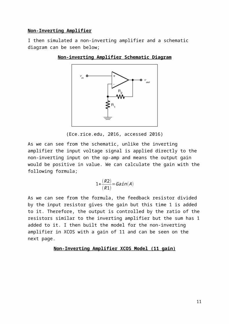
Non-Inverting Amplifier
I then simulated a non-inverting amplifier and a schematic diagram can be seen below;
Non-inverting Amplifier Schematic Diagram
(Ece.rice.edu, 2016, accessed 2016)
As we can see from the schematic, unlike the inverting amplifier the input voltage signal is applied directly to the non-inverting input on the op-amp and means the output gain would be positive in value. We can calculate the gain with the following formula;
1+(R 2)(R 1)
=Gain (A )
As we can see from the formula, the feedback resistor divided by the input resistor gives the gain but this time 1 is added to it. Therefore, the output is controlled by the ratio of the resistors similar to the inverting amplifier but the sum has 1 added to it. I then built the model for the non-inverting amplifier in XCOS with a gain of 11 and can be seen on the next page.
9

Non-Inverting Amplifier XCOS Model (11 gain)
As we can see the feedback resistor was set to 10KΩ and R1 set to 1KΩ, which should give an output signal 11 times greater than the input. So when we use the formula from the previous page we can calculate what the expected output should be.
1+(R 2)(R 1)
=Gain (A )
1+ 100001000
=11
Gain=11
I then ran the simulation and the scope results can be seen below.
Non-Inverting Amplifier Scope Results (11 gain)
As we can see from the scope results above, the output gain was 11 which proved that the circuit was working as a non-inverting amplifier.
10
Next I was tasked with varying the gain to 1, 2 and 20. Below is the model for a gain of 1.
Non-Inverting Amplifier XCOS Model (1 gain)
As we can see from the picture above R1 was set to 100KΩ and R2 was set to 1KΩ. Therefore, when using the formula from the previous page we can calculate what the output gain would be.
1+(R 2)(R 1)
=Gain (A )
1+ 1000100000
=1.01
Gain=1.01
As the ratio of the resistors can never be zero, 1.01 is the closest to 1 that I could simulate without increasing the value of resistance further. Next I ran the simulation and below are the scope results.
Non-Inverting Amplifier Scope Results (1 gain)
11

As we can see from the scope results on the previous page the output gain is around 1. Next I altered the values for the resistors to produce a gain of 2 and below is a picture of the XCOS model.
Non-Inverting Amplifier XCOS Model (2 gain)
As we can see from the picture above R2 and R1 was set to 1KΩ therefore when using the formula, we can calculate what the output gain would be.
1+(R 2)(R 1)
=Gain (A )
1+ 10001000
=2
Gain=2
Next I ran the simulation and below are the scope results.
Non-Inverting Amplifier Scope Results (2 gain)
12

As we can see from the scope results on the previous page the output gain is exactly 2. Next I altered the values for the resistors to produce a gain of 20 and below is a picture of the XCOS model.
Non-Inverting Amplifier XCOS Model (20 gain)
As we can see from the picture above R2 was set to 19KΩ and R1 was set to 1KΩ. Therefore, when using the formula from the previous page we can calculate what the output gain would be.
1+(R 2)(R 1)
=Gain (A )
1+ 190001000
=20
Gain=20
I then ran the simulation and below are the scope results.
Non-Inverting Amplifier Scope Results (20 gain)
13

As we can see from the scope results on the previous page the output gain is exactly 20.
Non-Inverting Buffer
Next I simulated a non-inverting amplifier and a schematic diagram can be seen below;
Non-Inverting Buffer Schematic Diagram
(Open Music Labs, 2016, accessed 2016)
The non-inverting buffer is a single input device which has a gain of 1, mirroring the input at the output. It has value for impedance matching and for isolation of the input and output. Therefore, a Buffer is an amplifier which has a gain of unity, a high input impedence and low output impedence. It can be used as a bridge between two circuits, where one circuit has a high output impedence and the other circuit has a low input impedence. The buffer would prevent the second circuit from interfering with the first circuit working correctly. We can calculate the gain with the following formula;
Gain ( A )=(Vout )(Vin)
=+1
I then built the model for the non-inverting buffer in XCOS and can be seen below.
Non-Inverting Buffer XCOS Model
14

As we can see in the picture on the previous page, the feedback loop is without a resistor therefore this creates direct feedback so the gain should be equal to 1. The buffer can replicate weak signals however it can drive enough current to be further amplified if needed. I then ran the simulation and below are the scope results.
Non-Inverting Buffer Scope Results
As we can see from the scope results that the output signal gain is equal to 1, as the output was the same as the input.
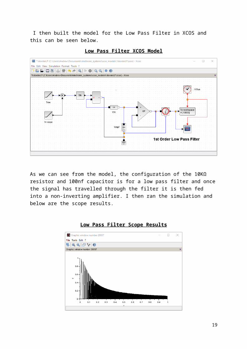
Low Pass Filter
Next I simulated a 1st Order Low Pass Filter and a schematic diagram can be seen below;
1st Order Low Pass Filter Schematic Diagram
15

(Electronicshub.org, 2015, accessed 2016)
A first-order low pass active filter consists simply of a passive RC filter stage providing a low frequency path to the input of a non-inverting buffer giving it a DC gain of one, Av = +1 or unity gain. The cut off frequency for a low pass filter can be calculated with the following formula;
12π RC
=Cut off frequency
I then built the model for the Low Pass Filter in XCOS and this can be seen below.
Low Pass Filter XCOS Model
As we can see from the model, the configuration of the 10KΩ resistor and 100nf capacitor is for a low pass filter and once the signal has travelled through the filter it is then fed into a non-inverting amplifier. I then ran the simulation and below are the scope results.
Low Pass Filter Scope Results
16

This information could be analysed further by using a program to process the matrix A in the workspace. I then executed the program FFTProg.sce in the Scilab console window. This program will print the matrix, plot it and show the Fast Fourier Transform (FFT). The FFT scope results can be seen on the next page.
Low Pass Filter FFT Scope Results(a)
Low Pass Filter FFT Scope Results(b)
17

From these FFT scope results, I could see the circuit was acting as a Low-pass filter allowing the lower frequencies to pass while beginning to block the signal at around 110KHz.
High Pass Filter
Next I simulated a 1st Order High Pass Filter and a schematic diagram can be seen below;
1st Order High Pass Filter Schematic Diagram
(Electronicshub.org, 2015, accessed 2016)
As we can see from the schematic diagram, a first-order high pass active filter consists simply of a passive CR filter stage providing a high frequency path to the input of a non-inverting buffer giving it a DC gain of one, Av = +1 or unity gain. The cut off frequency for a high pass filter can be calculated with the following formula;
18
12π RC
=Cut off frequency
I then built the model for a high pass filter in XCOS and this can be seen below.
High Pass Filter XCOS Model
As we can see from the model, the configuration of the 100nf capacitor and 10KΩ resistor is for a high pass filter and once the signal has travelled through the filter it is then fed into a non-inverting amplifier. I then ran the simulation and the scope results can be seen on the next page.
High Pass Filter Scope Results(a)
High Pass Filter Scope Results(b)
19

This information could be analysed further by using the FFT program to process the matrix A in the workspace. I then executed the program FFTProg.sce in the Scilab console window. This program then printed the matrix, plotted it and showed the FFT. The FFT scope results can be seen on the next page.
High Pass Filter FFT Scope Results(a)
High Pass Filter FFT Scope Results(b)
20

From these FFT scope results, I could see the circuit was acting as a high pass filter allowing the higher frequencies to pass while beginning to block the signal at lower frequencies.
Band Pass Filter
Next I simulated a 1st Order Band Pass Filter and a schematic diagram can be seen below;
1st Order Band Pass Filter Schematic Diagram
(Electronics Tutorials, 2016, accessed 2016)
As we can see from the schematic diagram, a first order band pass active filter consists simply of a passive CR high pass filter combined with a passive RC low pass filter. The cut off frequencies for low pass and high pass filters can be calculated with the following formula;
12π RC
=Cut off frequency
These 2 cut off frequencies are then combined to create a band pass where the cut off frequency for the high pass filter would be the start of the band pass and the cut off frequency for the low pass would be the end of the band pass. Therefore, only signals above or below these two cut off frequencies would be allowed to pass through the circuit. I then built the model for a band pass filter in XCOS and this can be seen on the next page.
Band Pass Filter XCOS Model
21

As we can see from the model, the configuration of the high pass filter and then the low pass filter. I then ran the simulation and the scope results can be seen on the below.
Band Pass Filter Scope Results(a)
Band Pass Filter Scope Results(b)
22

The information from the scope results could be analysed further by using the FFT program to process the matrix A in the workspace. I then executed the program FFTProg.sce in the Scilab console window. This program then printed the matrix, plotted it and showed the FFT. The FFT scope results can be seen below.
Band Pass Filter FFT Scope Results(a)
Band Pass Filter FFT Scope Results(b)
From these FFT scope results, I could see the circuit was acting as a band pass filter.
23

Next I was tasked with investigating Butterworth and Chebyshev filters.
Butterworth Filters
The Butterworth filter is a type of filter used in signal processing and it is designed so the passband has a frequency response that is as flat as possible. The response has no ripples in the response because the passband is designed to have a frequency response which is as flat as mathematically possible from 0Hz until the cut off frequency at -3Db with no ripples. Therefore, the Butterworth design ensures a flat response in the pass band and an adequate roll off. This reason makes the Butterworth filter, the ideal filter to use in audio circuits. The gain for the filter can be calculated with the following formula;
H ( jω )= 1
√1+E ²( ωωp
) ² ⁿ
I then built a second order low pass Butterworth filter in XCOS and this can be seen in the picture below.
2 nd Order Butterworth Low Pass Filter
As we can see from the model, the configuration of the 1KΩ resistors and 10nf capacitor is for a second order low pass filter and once the signal has travelled through the filter it is then fed into a non-inverting amplifier. I then ran the simulation and below are the scope results.
2 nd Order Butterworth Low Pass Filter Scope Results
24

The information from the scope results could be analysed further by using the FFT program to process the matrix A in the workspace. I then executed the program FFTProg.sce in the Scilab console window. This program then printed the matrix, plotted it and showed the FFT. The FFT scope results can be seen below.
2 nd Order Butterworth Low Pass Filter FFT Scope Results(a)
2 nd Order Butterworth Low Pass Filter FFT Scope Results(b)
25

As we can see from these results, the circuit is behaving like a low pass filter. However, the frequency response is similar to a Chebyshev response with a ripple and no matter what I tried I could not get the simulation to produce the response that was required. Therefore, I built the simulation in Multisim and this can be seen in the picture on the next page.
Butterworth Low Pass Filter Multisim Model
26

As we can see from the picture above I built the same 2nd order low pass circuit in Multisim I then ran the simulation and below is the a.c. sweep scope results.
Butterworth Low Pass Filter Multisim Scope Results
As we can see from these results in Multisim, the response looks more like a Butterworth response where the passband is a lot smoother. However, it still has a slight ripple near the cut off frequency and the roll off should be slightly steeper so it is still not reacting quite as expected.
Within Scilab or XCOS when you build and simulate circuits, code can be generated for the circuits. Also you can enter code within the Scilab console window to simulate various circuits and I will explain this further in Part 7. However, you can simulate the Butterworth filter frequency response by entering the following code;
//squared magnitude response of Butterworth filterh=buttmag(13,300,1:1000);mag=20*log(h)'/log(10);plot2d((1:1000)',mag,[2],"011"," ",[0,-180,1000,20])
After entering the above code and pressing return, the following response was achieved;
Butterworth Low Pass Filter Response Graph
27

As we can see from the graph above what the correct response for a Butterworth low pass filter should look like as there is a flat passband with no ripple and an adequate roll off.
Chebyshev Filters
Chebyshev filters are filters that have a steeper roll off and more of a passband or stopband ripple than Butterworth filters. They minimize the error between the idealised and the actual filter characteristic over a range of the filter but with ripples in the passband. There are two types of Chebyshev low pass filters. Type 1 has an all pole transfer function, where it has an equi-ripple passband and a monotonically decreasing stopband. A type 2 has both poles and zeros. Its band is monotonically decreasing and it has an equi-ripple stopband. By allowing some ripple in the passband or stopband magnitude response, a Chebyshev filter can achieve a steeper roll off than the same order Butterworth filter. This is the reason this type of filter is not used within audio circuits. The gain for both filters can be calculated with the following formulas;
Type 1
28

Gn ( ω)= 1
√1+E ²Tn² ( ωω0
)
Type 2
Gn ( ω,ω0 )= 1
√1+ 1
E ²Tn ²(ω 0ω
)
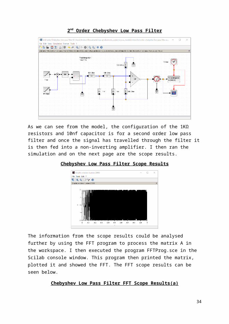
I then built a second order low pass Chebyshev filter in XCOS and this can be seen in the picture below.
2 nd Order Chebyshev Low Pass Filter
As we can see from the model, the configuration of the 1KΩ resistors and 10nf capacitor is for a second order low pass filter and once the signal has travelled through the filter it is then fed into a non-inverting amplifier. I then ran the simulation and on the next page are the scope results.
Chebyshev Low Pass Filter Scope Results
29

The information from the scope results could be analysed further by using the FFT program to process the matrix A in the workspace. I then executed the program FFTProg.sce in the Scilab console window. This program then printed the matrix, plotted it and showed the FFT. The FFT scope results can be seen below.
Chebyshev Low Pass Filter FFT Scope Results(a)
Chebyshev Low Pass Filter FFT Scope Results(b)
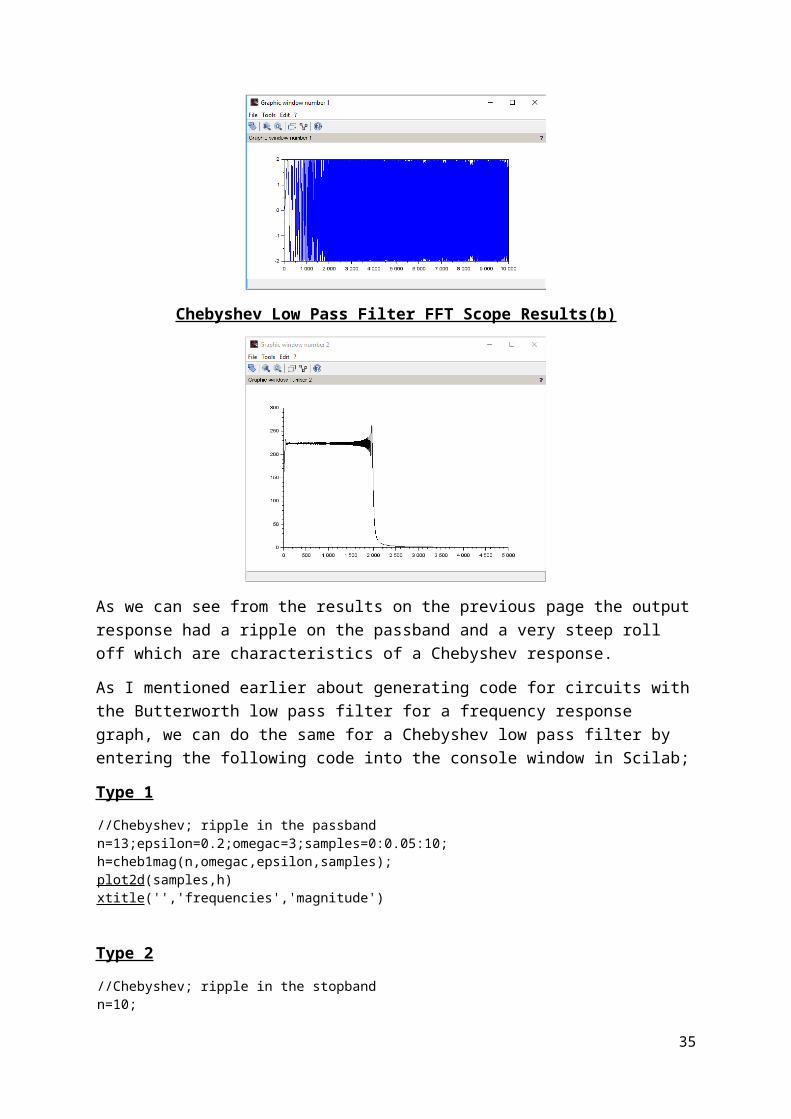
As we can see from the results on the previous page the output response had a ripple on the passband and a very steep roll off which are characteristics of a Chebyshev response.
As I mentioned earlier about generating code for circuits with the Butterworth low pass filter for a frequency response graph, we can do the same for a Chebyshev low pass filter by entering the following code into the console window in Scilab;
Type 1
//Chebyshev; ripple in the passbandn=13;epsilon=0.2;omegac=3;samples=0:0.05:10;h=cheb1mag(n,omegac,epsilon,samples);plot2d(samples,h)xtitle('','frequencies','magnitude')
Type 2
30

//Chebyshev; ripple in the stopbandn=10;omegar=6;A=1/0.2;Samples=0.0001:0.05:10;h2=cheb2mag(n,omegar,A,Samples);plot(Samples,log(h2)/log(10))xtitle("", "frequencies", "magnitude in dB");
//Plotting of frequency edgesminval=(-max(-log(h2)))/log(10);plot2d([omegar;omegar],[minval;0],[2],"000");
//Computation of the attenuation in dB at the stopband edgeattenuation=-log(A*A)/log(10);plot2d(Samples',attenuation*ones(Samples)',[5],"000")
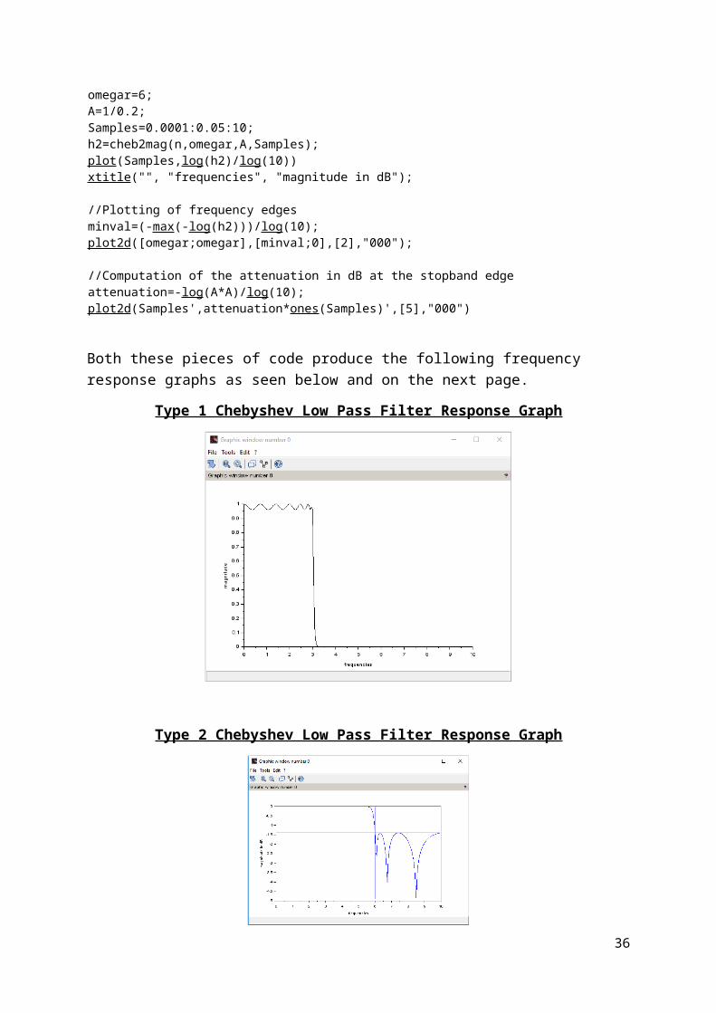
Both these pieces of code produce the following frequency response graphs as seen below and on the next page.
Type 1 Chebyshev Low Pass Filter Response Graph
Type 2 Chebyshev Low Pass Filter Response Graph
31

As we can see from the graph above and on the previous page what the correct responses for a Chebyshev low pass filter should look like. In type 1 there is a ripple present on the passband and in type 2 the ripple is after the passband.
Integrator
Next I investigated integrator and differentiator op amp circuits. An integrator is an op amp circuit that performs the mathematical operation of integration with respect to time, where we can cause the output to respond to changes in the input voltage over time as the op amp integrator produces an output voltage which is proportional to the integral of the input voltage. It integrates and inverts the input voltage Vin(t) over a time period t, t0, <t, <t1, producing an output voltage at time t = t1 of;
Vout ( t 1 )=Vout ( t 0 )− 1RC∫
t0
t1
Vin ( t ) dt
Vout=−1RC ∫
t0
t1
Vin ( t ) dt
Vout= −1jωRC
Vin
First I built the Integrator circuit in XCOS with a sinusoidal input and below is picture of that model.
Integrator Sine-wave XCOS Model
I then ran the simulation and below are the scope results.
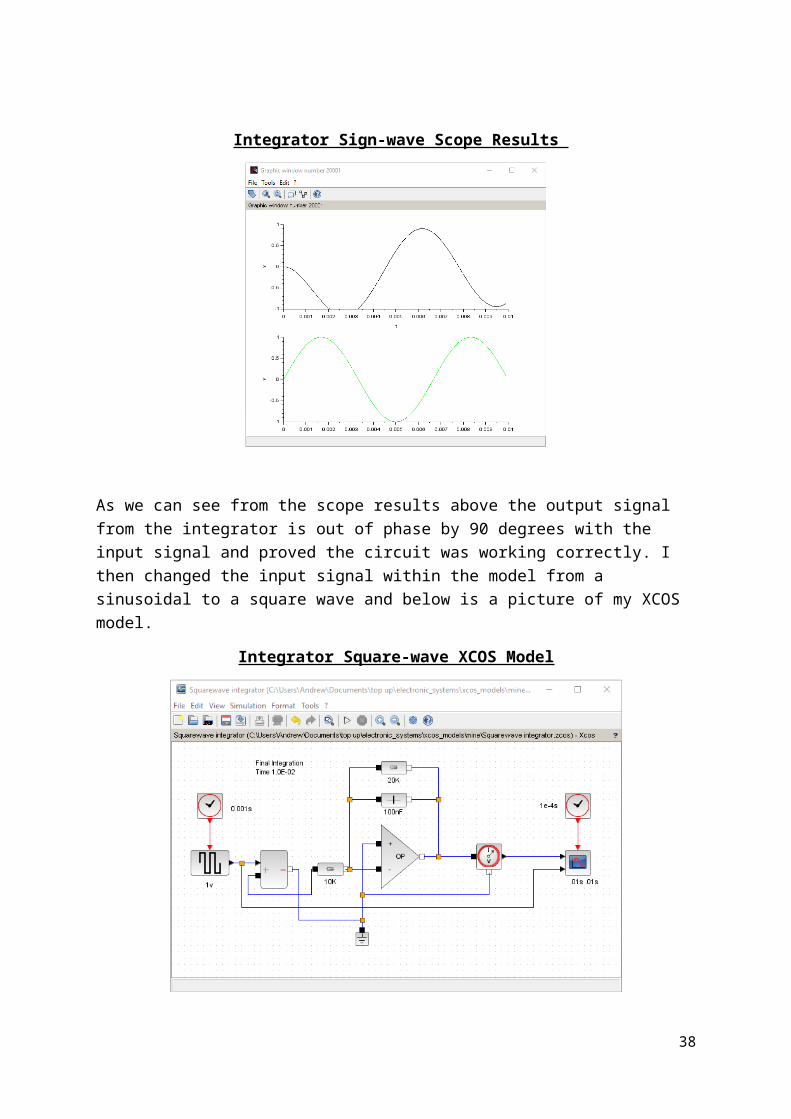
Integrator Sign-wave Scope Results
32

As we can see from the scope results above the output signal from the integrator is out of phase by 90 degrees with the input signal and proved the circuit was working correctly. I then changed the input signal within the model from a sinusoidal to a square wave and below is a picture of my XCOS model.
Integrator Square-wave XCOS Model
I then ran the simulation and the scope results can be seen on the next page.
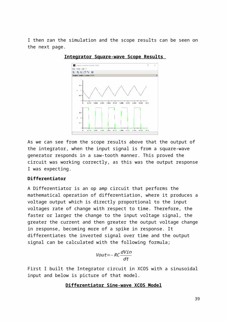
Integrator Square-wave Scope Results
33
As we can see from the scope results above that the output of the integrator, when the input signal is from a square-wave generator responds in a saw-tooth manner. This proved the circuit was working correctly, as this was the output response I was expecting.
Differentiator
A Differentiator is an op amp circuit that performs the mathematical operation of differentiation, where it produces a voltage output which is directly proportional to the input voltages rate of change with respect to time. Therefore, the faster or larger the change to the input voltage signal, the greater the current and then greater the output voltage change in response, becoming more of a spike in response. It differentiates the inverted signal over time and the output signal can be calculated with the following formula;
Vout=−RC dVindt
First I built the Integrator circuit in XCOS with a sinusoidal input and below is picture of that model.
Differentiator Sine-wave XCOS Model
I then ran the simulation and below are the scope results.
34
Differentiator Sine-wave Scope Results(a)
As we can see from the graph results above the output signal from the differentiator has changed from a sine wave to a cosine wave and the output is just a fraction of the input signal. I then changed the input signal within the model from a sinusoidal to a square wave and below is a picture of my XCOS model.
Differentiator Square-wave XCOS Model
I then ran the simulation and the scope results can be seen on the next page.
Differentiator Square-wave Scope Results
35
As we can see from the results above that when a square wave is inputted into a differentiator the output now has a spike on it and this is dependant, by the RC time constant. This proved the circuit was working correctly, as this was the output response I was expecting.
Differential Balanced Line Driver
A balanced line driver uses two wires for the signal, with the signal equal in amplitude in each wire and is opposite in phase. Only the out of phase signal is detected by the remote balanced receiver, and any in phase signal is rejected. Interference such as RF as well as other noise will be picked up equally by both wires in the cable and so will be in phase. It will therefore be rejected by the receiver. In this way, it is possible to have long interconnects, with a shield connected at one end only. By configuring the circuit like this it cuts the earth loop, and the balanced connection ensures that only the wanted signal is passed through to the amplifier. Therefore, a balanced line driver takes an unbalanced signal and converts it to a balanced signal. The balanced signal makes it easier to cancel out the noise, therefore leaving a clean signal. The main advantage of the balanced line format is it has good rejection of any external noise when fed to a differential amplifier.
The system usually uses twisted pair conductors to connect a transmitter with a receiver. A balanced line transmitter splits the signal and is usually fed into buffers, one to buffer the signal while the other is to buffer and invert the signal. This creates a balanced signal with the signal on both conductors where when the signal swings positive on one conductor it swings exactly the same amount negative on the other.
The balanced line receiver is a differential amplifier which amplifies the difference between the two input signals. By connecting one signal onto the inverting input and one signal to the non-inverting input the resultant output voltage will be proportional to the difference between the two input signals. The Vout of the differential amplifier can be calculated with the following formula;
Vout=R3R1
(V 2−V 1)
36

In a balanced system the noise would be induced into the centre conductors and the shields signal equally but the noise is cancelled out because the noise is on both of the signal lines and the signal used by the amplifier in the receiver is the difference between the two signal lines. If the noise has a magnitude of 1.5V, the differential amplifier sees 1.5V minus 1.5V equals 0V. Balanced lines work because the noise from surrounding environment is induced into both wires equally and by measuring the difference between the two wires at the receiving end, the original signal can be recovered while the noise is cancelled.
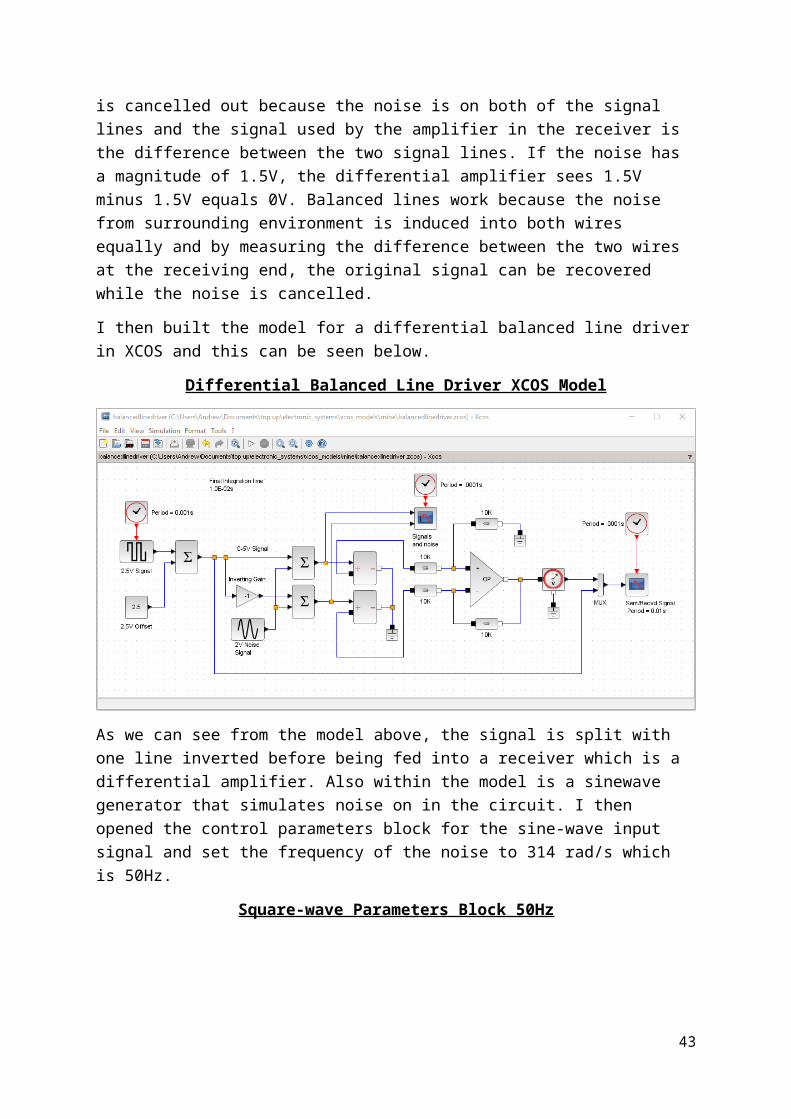
I then built the model for a differential balanced line driver in XCOS and this can be seen below.
Differential Balanced Line Driver XCOS Model
As we can see from the model above, the signal is split with one line inverted before being fed into a receiver which is a differential amplifier. Also within the model is a sinewave generator that simulates noise on in the circuit. I then opened the control parameters block for the sine-wave input signal and set the frequency of the noise to 314 rad/s which is 50Hz.
Square-wave Parameters Block 50Hz
I then ran the simulation and the scope results can be seen on the next page.
37
Differential Balanced Line Driver 2V 50Hz Noise Signal Scope Results
As we can see from the above results the two lines have the signal on them however they are in anti-phase and are beginning to show some effects of noise with the slight curve of the signal. The output signal that was achieved was smooth with no signs of noise and was amplified up from 5V to 10V. This proved the circuit was working correctly and below is a picture of those results.
Differential Balanced Line Driver Input & Output Signal Scope Results
I then opened the control parameters block for the sine-wave input signal and set the frequency of the noise to 15000 rad/s which is 2387Hz. This can be seen on the next page.
38
Square-wave Parameters Block 2387Hz
I then ran the simulation and the scope results can be seen below.
Differential Balanced Line Driver 2V 2387Hz Noise Signal Scope Results
As we can see from the above results, now that the frequency has been increased the two lines clearly have noise on them and equal amounts of noise is seen on both However, the output signal that was achieved was smooth with no signs of noise and was amplified up from 5V to 10V. This proved the circuit was working and below is a picture of those results.
Differential Balanced Line Driver 2V 2387Hz Input & Output Signal Scope Results
39

I then opened the control parameters block for the sine-wave input signal and set the frequency of the noise to 30000 rad/s which is 4775Hz. This can be seen below.
Square-wave Parameters Block 4775Hz
I then ran the simulation and the scope results can be seen below.
Differential Balanced Line Driver 2V 4775Hz Trace Scope B
As we can see from the above results, now the frequency of the noise has been increased even more, the signals are showing more distortion and equal amounts of noise on both. However, the output signal that was achieved was smooth with no signs of noise and was amplified up from 5V to 10V. This proved the circuit was working and on the next page is a picture of those results.
40

Differential Balanced Line Driver 2V 4775Hz Trace Scope A
RS-485
RS-485 allows multiple devices to communicate at half-duplex on a single pair of wires plus a signal ground wire at distances up to 1200 meters. The function of the signal ground wire is to tie the signal ground of each of the nodes to one common ground. With RS-485, both the length of the network and the number of nodes can easily be extended using a variety of repeater products on the market. On this network data is transmitted differentially on two wires twisted together and this is referred to as a twisted pair. The properties of differential signals provide high noise immunity and long distance capabilities. Only one device at a time can drive the line so when the drivers are not in use they must be put into a high-impedance mode. Some RS-485 hardware handles this automatically and in other cases the RS-485 device software must use a control line to handle the driver. RS-485 software handles addressing, turn-around delay, and possibly the drivers tri-state features of RS-485.
Throughout this part of my investigations I learned about various ways op amps can be configured to obtain a desired output response and was able to simulate all of the circuits successfully. Within XCOS, the Butterworth filter was tricky to tune so the output response was smooth and without ripples. However, I believe I built a model in Multisim that produces an output that is adequate.
41

Part 2
Blood Pressure Monitor
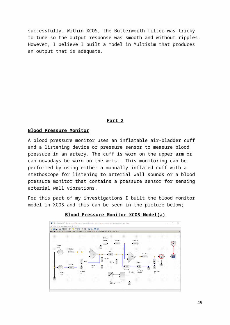
A blood pressure monitor uses an inflatable air-bladder cuff and a listening device or pressure sensor to measure blood pressure in an artery. The cuff is worn on the upper arm or can nowadays be worn on the wrist. This monitoring can be performed by using either a manually inflated cuff with a stethoscope for listening to arterial wall sounds or a blood pressure monitor that contains a pressure sensor for sensing arterial wall vibrations.
For this part of my investigations I built the blood monitor model in XCOS and this can be seen in the picture below;
Blood Pressure Monitor XCOS Model(a)
In the model as seen above there is a voltage source to simulate a heartbeat and another voltage source to simulate noise on the circuit. The two signals are then combined and after the microphone signal has been buffered, it is then passed through a low pass filter. Next is a ramp function that simulates the signal from the arm cuff. I then ran the simulation and the scope results can be seen below.
Blood Pressure Monitor Trace
42
These results simulate a response from a blood pressure monitor and the teeth in the output represent heart beats. The plot shows the rise in pressure from the arm cuff accompanied by the heart beats monitored by a microphone.
I then replaced the 15KΩ resistor that is connected to the heartbeat mains voltage supply with a variable resistor and this can be seen in the picture below;
Blood Pressure Monitor XCOS Model(b)
As we can see from the model above that I replaced the resistor with a variable resistor and set the resistance to 50KΩ. I then ran the simulation and below are the results.
Blood Pressure Monitor Variable Resistor 50KΩ Scope Results
As we can see from the above results that by increasing the resistance of the variable resistor, then this reduces the heart beat signals.
Next I increased the resistance to 100KΩ and then 200KΩ and the results can be seen on the next page.
43

Blood Pressure Monitor Variable Resistor 100KΩ Scope Results
Blood Pressure Monitor Variable Resistor 200KΩ Scope Results
As we can see from both sets of results, that when the resistance is increased this reduces the heartbeat signals. Also when I injected noise into the circuit and the higher the frequency that was inputted, then the simulation took longer to finish running.
Throughout this part of my investigations I learned about a blood pressure monitor and how by simulating the pressure in the arm cuff with resistance on the circuit causes the output to become smoother. Also the simulation produced the correct response which proved I had simulated it correctly.
44

Part 3
Simple AM Receiver
Amplitude modulation is used in a variety of applications. Although it is not as widely used as it was in previous years, it can still be found within broadcast transmissions or air band radio to name a couple.
Amplitude modulation (AM) is a method of injecting data onto an alternating current (AC) carrier signal. The highest frequency of the modulating data is normally less than 10 percent of the carrier frequency. The instantaneous amplitude (overall signal power) varies depending on the instantaneous amplitude of the modulating data. This moves the information signal to a new location which is above and below the carrier frequency. These components are called the USB Upper Sideband and LSB Lower Sideband and they are a mirror image of each other.
Below is an equation which shows how AM works;
Vc(t) = Ac(1 + Am sinωmt) sinωct
This can be simplified to the equation below;
Vc(t) = (1 + msinωmt) sinωct
Vc(t) is the term for the modulated carrier wave form and the part of the equation that is highlighted in red is the amplitude term with an average value of one and will increase +m or -m from that value. Also ωm is the modulated frequency and ωc is the carrier signal in rad/secs so the amplitude of the carrier wave is being modulated by the information wave.
For this part of my investigations I built a simple AM receiver model in XCOS and this can be seen in the picture below;
Simple AM Receiver XCOS Model
45

As we can see from the model on the previous page the simple AM receiver is made up of sub-systems. They are the information signal and carrier which produces the AM signal. Next is an envelope detector that is followed by a low pass filter. Then there are the bias resistors feeding the signal into a buffer and the last sub-system is an inverting amplifier.
The analogue information signal is supplied by a sinusoidal generator and this generates a tone at the angular frequency of the information signal which was set to 5KHz. This is then added to a constant of 1 and is multiplied by a carrier signal that was set to 100KHz.
This creates an AM signal that is fed into the envelope detector which is a diode and a low pass filter. This diode detects the signal by first rectifying the AM carrier so the AM signals value are no longer zero and because the received signals are weak, diodes with very low turn on voltages are used. Then the half wave rectified pulses are fed through a low pass filter and are therefore smoothed, so the carrier frequency is removed and the slowly changing envelope is obtained as an output.
The biasing in this circuit is similar to voltage divider biasing, however this circuit uses an op amp to buffer the bias voltage and this can help cut down on consumption of power within the circuit. This will give a more accurate gain as well as offset values because the impedance produced from the biasing and the op amp, that is fed into the rest of the circuit will be negligible compared to another method. It also can produce to numerous circuits, a bias voltage that is very stable and removes any cross coupling between the circuits signals.
Finally, the output from the buffer is fed into an inverting amplifier where the demodulated signal is amplified.
I then ran the simulation and the results can be seen below as well as the next couple of pages.
AM Receiver Information Signal Scope Results
46

AM Receiver Modulated Signal Scope Results
As we can see from the scope results above and on the previous page that when an amplitude modulated signal is created, the amplitude of the signal is varied in line with the variations in intensity of the sound wave. In this way the overall amplitude or envelope of the carrier is modulated to carry the audio signal.
From the results above we can clearly see 100% modulation on the carrier signal and the information signal can be seen to change in line with the carrier signal. When the information signal is maximum (1) the modulated signal is maximum (2V) and when it is minimum (-1) the modulated signal is minimum (0V).
The next two sets of scope results show the demodulated and final output signals, which can be seen below as well as the on the next page.
AM Receiver Demodulated Signal Scope Results
47

AM Receiver Output Signal Scope Results
The demodulated signal scope results show the half wave rectified signal has been attempted to be reconstructed by the filter. However, the output signal is not smooth but contains fluctuations within it and this is caused by the values of the resistor as well as the capacitor.
In the final graph the final output signal can be seen to have increased in output therefore it must have been amplified by the final inverting op amp within the circuit.
Throughout this part of my investigations I learned about the different subsystems within an AM receiver and how it works. Also the simulation produced the correct response which proved I had simulated it correctly.
48
Part 4
Switch Mode Power Supply
Flyback converters are used to convert AC to DC and DC to DC with galvanic isolation between the input and any outputs. It is derived from a buck-boost converter where the Inductor is split and acts like an isolation transformer. This means that the ratios of voltage are multiplied with the advantage of isolation. So because it is similar to a boost converter the principles of both converters are similar.
When the switch is activated, an input voltage would be connected to the primary side of the transformer. Due to this the current and magnetic flux in the primary side increase storing energy in the transformer. Now because of this, a negative voltage is induced into the secondary side of the transformer making the diode reverse biased (due to the winding polarities) and output load receives energy from the output capacitor. If the switch is then deactivated, the magnetic flux and current in the Primary side of the transformer will drop. Then the voltage on the Secondary side of the transformer is turned to positive and therefore forward biasing the diode and allowing current to flow. Any energy stored in the core of the transformer then recharges the capacitor which supplies the load.
So a Flyback converter is an isolated converter and will also need isolation of the control circuit. The control circuit is made up of the voltage and current mode control and both need a signal related to the output voltage.
For this part of my investigations I built a Flyback converter model in XCOS and this can be seen in the picture below
Flyback Converter XCOS Model
I set the input voltage to 240V, then ran the simulation and the scope results are on the next page.
49

Flyback Converter Scope Results
As we can see from the above results the output voltage is just below 100V compared to the 240V inputted into the circuit. Also the output current is spiking up to around 30A at every step of the switch, switching on.
One advantage of the Flyback converter circuit over the other switched mode power supplies is that many of them need a separate inductor for storage. Therefore, since the transformer in a Flyback converter is the storage inductor, there is no need for a separate one. This along with the fact that the rest of the Flyback converters circuitry is simple makes the Flyback converter a cost effective and extremely popular within industry. Another advantage is it has greater efficiency as the transistor or mosfet loses little power when switching. There are also other advantages such as they are smaller as well as lighter in weight and produce lower heat due to their higher efficiency.
I tried to apply feedback to the system to control the level of output, however I could not get the simulation to work and below is a picture of the model.
Flyback Converter feedback XCOS Model
Throughout this part of my investigations I learned about a Flyback converter and the advantages of isolated power supplies. I could not get the feedback model to work and will revisit this at a later date.
50

Part 5
PID Controller
A Proportional Integral Derivative (PID) controller is a control loop used throughout industrial control systems and is the most commonly used as a feedback controller. It calculates the value of error by comparing the output with the input. The calculation involves three separate constant parameters and they are known as a three term control. They are the proportional, the integral and the derivative values. These values can be interpreted in terms of time. Proportional (P) depends on the present error, integral (I) depends on the accumulation of past errors, derivative (D) is the prediction of future errors, based the rate of change of the current. The sum of these actions is applied to alter the process via a control element like say a valve of a heating element. The three terms can be calculated wit following formulas;
ProportionalOutput=¿ Kp e(t)
IntegrationOutput=Ki∫0
t
e ( t ) dt
DerivativeOutput=Kd ddt
e (t )
When adding these three formulas together you can calculate the output of the PID controller as seen below;
PIDControllerOutput=Kp e(t )+Ki∫0
t
e ( t )dt+Kd ddt
e (t)
I then built the model for a PID controller in XCOS and this model can be seen in the picture below.
PID Controller XCOS Model(a)
51

I then ran the simulation but it would not complete indicating an error in the circuit. Therefore, I built an alternative model and this can be seen below.
PID Controller XCOS Model(c)
As we can see in the model, the three sub-systems of a PID controller with a step input. I then ran the simulation and below are the results.
Proportional, Integral and Derivative Scope Results(a)
As we can see from the results above, they are the outputs of the individual sub-systems and the top results are for the proportional amplifier which shows an output of 1 when the step activates at 0.1 seconds. This is correct as the gain was set to 1. The middle results are for the integration amplifier and these results show an output of 10 when the step activates. The bottom results are for the derivative amplifier and these results show the output rising from 0 in a linear fashion after the step is activated at 0.1 seconds. All three results are added together to give the final PID output signal these results can be seen on the next page.
52

Final PID Output Signal Scope Results(a)
As we can see from the above results that the final output signal is the sum of all three signals from the earlier results. Here the output is around 11 and rising in a linear fashion over time. This is the 1 output from the proportional amplifier, 10 output from the integration amplifier and the linear characteristic rise in output from the derivative amplifier added together.
In the model I then changed the values for the proportional to 0.4, integral to 4 and derivative to 0.5 and this can be seen in the picture below.
PID Controller XCOS Model(c)
I then ran the simulation and on the next page are the results.
53

Proportional, Integral and Derivative Scope Results(b)
As we can see from the results on the previous page, the different signals from the sub-systems and below are the results of the final output from the PID controller.
Final PID Output Signal Scope Results(b)
The results above show us the sum of the three sub-systems which is around 5 and rising in a linear fashion.
I then built a model for a PID controller, however I used the individual op amp circuits that make up the three sub-systems. By connecting an inverting amplifier with an integrator amplifier and differentiator amplifier. This is then connected to a summer amplifier to add the three signals together and a picture of that model can be seen on the next page.
54

Analogue PID Controller XCOS Model
I then ran the simulation and below as well as on the next page are the results
Proportional Output Signal Scope Results
Integral Output Signal Scope Results
55

Derivative Output Signal Scope Results
As we can see from the results on the previous page the results for the proportional, integral as well as derivative outputs and below is the final PID results.
Final PID Output Signal Scope Results
The above results show the sum of the three sub-systems that are within the PID controllers output. As we can see it has a steep ramp when the step is activated at 0.1 seconds and is also showing signs of an overshoot with a peak before levelling out with an output of around a value of 4.
Throughout this part of my investigations I learned about the different subsystems within a PID controller with regards to the proportional, integration and differentiator amplifiers. I also learned how to calculate the output responses of each amplifier. Also the simulations produced the correct response which proved I had simulated it correctly.
56

Part 6
Music Circuit
For this part of my investigations I was tasked to research a music amplifier or fuzzbox and build a simulation model from the circuit diagram as seen below.
Music Circuit Diagram
(Whitbread 2016, accessed 2016)
From the circuit diagram we can see what a basic system looks like. In this system the signal is fed into non-inverting amplifier that is AC coupled with split resistors and below is a picture of its circuit diagram.
AC Coupled Non-Inverting Amplifier with Split Resistors
(Poole, 2016, accessed 2016)
An AC coupled amplifier has the bias voltage connected to the non-inverting input and the bias is simply the voltage we would expect to see at the output when no signal is applied. Within this configuration it is important that the values of the resistors and capacitors are applicable for the frequencies required. The gain, cut off frequency and output of this op amp can be calculated with the following formulas on the next page;
57

Vb= R4R3+R 4
Vs
Bias Resistance (R5)=R3 x R4R3+R 4
Gain=1+(R2R1
)
fc= 1(2 π)(R 5 xC 1)
Vo=GVi+Vb
The transistors in the music circuit operate such that one conducts for the positive half cycle and the other conducts for the negative half cycle, thus producing a full cycle of output signal. This high power output signal from the transistors is then used to drive a speaker or subwoofer of low impedance. Therefore, when a small input current is fed between the base and emitter, you get a much larger output current flowing between the emitter and the collector. So the weak signal is fed into the base and you use the output from the collector to drive a speaker. The biasing for the transistors is provided by the diodes as well as the 1KΩ resistors. This arrangement biases the transistors just above cut off and reduces the crossover distortion.
I then built the model in XCOS and below is a picture of that model.
Music Circuit XCOS Model
58

I then ran the simulation however the simulation did not produce the desired output and I received an error message which are shown below;
Scilab Error Message
Music Circuit Scope Results
Clearly there is a problem which I think is a timing problem within the simulation and whatever I try, the problem could not be rectified. Therefore, I built the same circuit within Multisim and below is a picture of that model.
Music Circuit Multisim Model
59

I then set the frequency to 6kHz which can be seen in the picture below;
Function Generator Parameters Block
Next I ran the simulation and below are the results I achieved.
Music Circuit Output Scope Results
60

As we can see from the above results the smaller trace is the input signal and the bigger one is the output signal. It is clear that the input signal has been amplified as it is now around twice as big as the input signal.
Throughout this part of my investigations I learned about the different sections within a music amplifier. I learned about an AC coupled non inverting amplifier with split resistors and how to calculate the output response. Even though I could not achieve an adequate response in XCOX, I believe I built a model in Multisim that produces an output that is adequate.
Part 7
Code Generation
As I mentioned earlier, C code can be generated by building and simulating models. Where the code for a specific function can be inputted into Scilab such as a filter, like for the response of the Butterworth filter at the end of part 1 and even the FFT program used in the filter investigations is generated from code. The FFT file can be opened in SciNotes and this can be seen below.
FFT Code
61

To generate code for a specific model I first needed to download some software call X2C which is an open source code generator for Scilab/XCOS and then I followed the installation instructions to pair X2C with Scilab. This loaded the X2C libraries into the Scilab console window and within the file explorer I loaded a demo model for an LED that was to be switched on and off with a square-wave input. The path of the location for the demo is in the picture below and a picture of the demo model is on the next page.
Scilab File Browser(a)
X2C Demo Model Generated in XCOS
62

I then double clicked on the start communicator box which opened the controller and then I double clicked on the other orange box which loads it into the controller. Next I clicked the create code tab on the controller and this created the files, X2C.c and X2C.h. This can be seen in the picture below;
Scilab File Browser(b)
Next I right clicked on both files, then opened both files in SciNote and the X2C.c files code can be seen on the next few pages.
X2C.c Code
63

X2C.c Code (continued)
64

X2C.c Code (continued)
65

As we can see from the previous couple of pages the code that has been generated and this along with the X2C.h file can be uploaded into software like MPLabX for example, where it can be uploaded into a microcontroller via a programmer or development board. With some changes to the code the model could be altered to react differently and this is handy when time is limited to build a new circuit.
Throughout this part of my investigations I learned about how C code can be generated from different models with XCOS and X2C. This extremely handy as you can simulate numerous models, then convert the model to code and upload the code to a microcontroller.
Conclusion
66

To conclude these investigations went well and I learned a lot. Electronic systems are all around us and an important part of the modern world. This report introduced me to ways, to control the output of circuits such as how the various ways an op amp can be configured to produce a desired response. I also learned that simulation software was excellent for the purpose of my investigations and I believe I was successful acquiring the correct output responses.
As mentioned, I learned about the various ways to control the output of op amps and the different configurations the op amps can be connected in. I simulated various filters, learned how to calculate the cut off frequencies and about how balanced line drivers remove noise from the system. I also covered a blood pressure monitor learning how it works and the effect of noise on the system.
With the AM receiver simulation, the outputs showed me the information signal being fed into the circuit and when combined with a carrier signal the output is a modulated signal. It is then demodulated and this signal is amplified ready to be received. I also learned about the various parts of the AM receiver circuit and what their operation was.
The Flyback converter simulation taught me about switched mode power supplies and the advantages that comes with the circuit. I also learned about PID controllers, with their individual sub-systems that combine to create the PID output that was expected and how it can be constructed using op amps with proportional, integration and differentiator amplifiers.
My investigations of the music circuit, was difficult as I could not get the simulation to run in XCOS, however I did manage to simulate the circuit in Multisim where I learned about an AC coupled inverting amplifier with split resistors and what the function of the transistors within the circuit was.
Finally, with regards to code generation I learned that with the assistance of X2C software, which is a code generator for Scilab/XCOS, I can build a model and then convert it into some C code. This code can then be opened in some software like MPLabX and then be uploaded into a microcontroller via a programmer or development board.
All together I have learned a lot this semester and although XCOS was tricky to use, I still simulated almost all circuits in XCOS. If I could not, I used Multisim to complete my investigations and it should hold me in good stead throughout what I hope to be a long career, because electronic systems are embedded throughout industry.
References
67

Ece.rice.edu. (2016) Experiment 5.2 Voltage Amplifiers. [Internet], Available from: <http://www.ece.rice.edu/~jdw/243_lab/exp5.2.html> [Accessed 28th April 2016].
Electronicshub.org. (2015) Active Low Pass Filter. [Internet], Available from: <http://www.electronicshub.org/active-low-pass-filter/> [Accessed 30th April 2016].
Electronics Tutorials. (2016) Passive Band Pass Filter. [Internet], Available from: <http://www.electronics-tutorials.ws/filter/filter_4.html> [Accessed 30th April 2016].
Open Music Labs. (2016) Op-Amps: Part ii. [Internet], Available from: <http://www.openmusiclabs.com/learning/analog/op-amps-part-ii/> [Accessed 28th April 2016].
Poole, I. (2016) Non-inverting amplifier circuit using an op-amp. [Internet], Available from; <http://www.radio-electronics.com/info/circuits/opamp_non_inverting/op_amp_non-inverting.php> [Accessed 28th April 2016].
Stack Exchange Inc. (2016) Inverting buffer with op-amps. [Internet], Available from: <http://electronics.stackexchange.com/questions/148356/inverting-buffer-with-op-amps> [Accessed 28th April 2016].
Whitbread, M, (2016) Electronic Systems: Module Handbook. [Internet], Available from: <Moodle> [Accessed 28th April 2016].
68