Embed Size (px)
Citation preview

Appl Phys A (2012) 107:1–11DOI 10.1007/s00339-012-6856-z
I N V I T E D PA P E R
Electronic structure and transport measurements of amorphoustransition-metal oxides: observation of Fermi glass behavior
I. Goldfarb · F. Miao · J. Joshua Yang · W. Yi ·J.P. Strachan · M.-X. Zhang · M.D. Pickett ·G. Medeiros-Ribeiro · R. Stanley Williams
Received: 26 February 2012 / Accepted: 26 February 2012 / Published online: 9 March 2012© Springer-Verlag 2012
Abstract We characterized the conduction mechanisms inthin sputtered films of three representative binary Me–O(Me = Ta, W, and Nb) systems as a function of oxy-gen content, by combining in situ chemical state and elec-tronic band structure studies from X-ray photoemissionwith temperature-dependent transport measurements. De-spite certain differences, these amorphous films all dis-played Fermi glass behavior following an oxidation-inducedtransition from metallic to hopping conduction, down toa sub-percolation threshold. The electron localization esti-mated from the band structure was in good agreement withthat from the transport measurements, and the two were usedto construct phase diagrams of conduction in the degree ofoxidation-conductivity coordinates, which should prove im-portant in the design of resistive switching and other elec-tronic devices.
1 Introduction
Transition metal oxides (TMO’s) have been long estab-lished as an important group of materials for a variety ofapplications, such as catalysis, gas sensing, and high-k di-electrics for gate capacitors in metal-oxide-semiconductor(MOS) technology. In particular, tungsten trioxide (WO3)is well known for its catalytic properties, gas sensitivity,
I. Goldfarb is on sabbatical leave from Faculty of Engineering,Tel Aviv University, Tel Aviv 69978, Israel.
I. Goldfarb (�) · F. Miao · J.J. Yang · W. Yi · J.P. Strachan ·M.-X. Zhang · M.D. Pickett · G. Medeiros-Ribeiro ·R.S. WilliamsHewlett-Packard Laboratories, 1501 Page Mill Road, Palo Alto,CA 94304, USAe-mail: [email protected]
electrochromism, suitability for solar cell technology, andhydrogen production [1–5] and oxides of Hf, Nb, and Tafor applications requiring high-k dielectrics and/or wide-gap semiconductors [6–8]. There has been a renewed in-terest in resistive switching for next generation non-volatilememory applications (e.g., resistance-change random ac-cess memory, RRAM) [9, 10] due to the recently identifiedmemristive behavior in numerous oxides, including those ofbinary TMO’s, such as Ti [11, 12], W[13], Ta [14], etc.,among which Ta-oxide has so far demonstrated superior per-formance in terms of switching speed, endurance, and en-ergy consumption [15, 16]. Thus the need to understand thephysics of electronic processes in TMO’s is timely, and mo-tivates numerous research efforts.
We investigated the evolution and transformations of con-duction mechanisms in transition-metal oxides during pro-gressive oxidation, by combining in situ core-level (CL)and valence band (VB) X-ray photoelectron spectroscopy(XPS) with ex situ temperature-dependent transport mea-surements, in order to see if there is a generic model of con-duction in TMO’s. For this purpose we chose three represen-tative Me–O systems; Ta–O, Nb–O, and W–O. The Ta–Osystem was chosen because it is one of the most promis-ing for memristive/resistive switching applications [15, 16]and it has a simple equilibrium phase diagram [17]. Thisdiagram contains only a single equilibrium oxide phase,tantalum-pentoxide (Ta2O5), and we believe this to be amajor reason for some of the excellent switching charac-teristics, such as very high endurance [15, 16]. The Ta–Osystem is representative of the class of TMO’s with the sim-plest binary diagrams, which also includes Hf–O, Ni–O, etc.Another class of TMO phase diagrams, including Nb–O,Mn–O, Fe–O, etc. [17] has intermediate phases with loweroxidation states (typically MeO and MeO2) than the ter-minal oxide. The Nb–O system was chosen to represent

2 I. Goldfarb et al.
this class because each of its phases exhibits a unique con-duction behavior: pure Nb is a superconductor, NbO ismetallic [18], NbO2 exhibits a metal-insulator transitionand a related negative differential resistance (NDR) [19–21], and Nb2O5 is a highly insulating dielectric. The lastclass of TMO’s, such as W–O, Ti–O, V–O, etc. [17] (rep-resented in this work by W–O) not only exhibits inter-mediate oxides of the MenOm stoichiometry, but the sub-stoichiometric “Magnéli phases”, as well, with compositiondefined by formulas of the type MenO2n−1 (e.g., Ti4O7)
or MenO3n−1 (e.g., W10O29), formed by the ordered ar-rangements of oxygen vacancies on crystallographic shearplanes [19].
Our findings demonstrate that all three TMO systems areFermi glasses over much of their composition ranges, inthe sense that they exhibit electron states at the Fermi levelthat are nevertheless localized due to oxidation-induceddisorder. Thus, their conduction is dominated by electronhopping between conduction centers until their concen-tration, upon increasing oxidation to the terminal oxide,falls below the critical threshold for percolation. Devia-tions from an idealized model were observed in Nb–O andW–O films, the two systems with more complex phase di-agrams, and attributed to the presence of stable mixed-valence oxidation states in those films, in contrast to Ta–Ofilms, underscoring the importance of systems with a sim-ple equilibrium phase diagram for reliable device perfor-mance.
2 Experimental
100–200 nm thick Ta–O, W–O, and Nb–O films were RF-sputtered in AJA International, Inc. magnetron sputteringsystem from elemental Ta, W, and Nb targets, respectively,onto commercially available 110 nm SiO2/p-Si(001) sub-strates, with 150 W at a dynamic pressure of 8 mTorr forTa (3 mTorr for W and Nb), Ar flow rate of 20 standardcubic centimeters per minute (sccm) for Ta (16 sccm forW and Nb) and O2 flow rates varying from 0 to 8 sccm.Prior to gas introduction, the chamber was evacuated to∼2 × 10⁻⁸ mbar. During the deposition the substrates wereheld at room temperature (RT) for W and Nb sputter-ing and ∼700 K (measured with optical pyrometer with±30 K accuracy) for Ta sputtering. Immediately after thedeposition films were in situ transferred into the analy-sis chamber of ESCA/Auger UHV apparatus by OmicronNanotechnology, GmbH (6 × 10⁻¹⁰ mbar base pressure)for X-ray Photoelectron (XPS) and Auger Electron (AES)spectroscopy. XPS analysis employed monochromated Alanode (1486.7 eV) and EIS-SPHERA hemispherical ana-lyzer. Absolute binding energy (BE) scale was calibratedby adjusting the spectrometer work function on Au 4f7/2
(BE = 83.98 eV) and Ag 3d5/2 (BE = 368.26 eV) spec-tral lines. The spectral resolution was determined by mea-suring full width at half maximum (FWHM) of the samelines to yield ∼0.6 eV at a 15 eV pass energy and ∼1.0 eVat 50 eV.
The spectra were normalized to eliminate inherent samp-le-to-sample intensity variations and some, particularly themore resistive ones, were also adjusted in BE to compen-sate for the charging-induced shifts, by fixing the O 1speak at 530.9 eV. After Shirley-type background subtrac-tion, the core-level (CL) 4f Ta and W (and 3d Nb) doubletswere deconvoluted using peak models based on a productof Gaussian and Lorentzian (GL) functions, as determinedby the best fit of the metallic and the terminal oxide dou-blets in the first and last samples in each series, respectively.(Combination of a tail modifier function with a GL peakshape was necessary to fit Nb–O samples to correct for theShirley asymmetry.) Additional parameters extracted fromthese metallic and fully oxidized CL fits were the 4f7/2–4f5/2 spin–orbit splitting of 1.90 eV for Ta and 2.15 forW, and 3d5/2–3d3/2 of 2.75 for Nb, 4f7/2/4f5/2 branchingratio of 1.15 for Ta and 1.33 for W, and 3d5/2/3d3/2 of1.45 for Nb, and FWHM peak broadening between 0.6 eV(metallic) and 1.6 eV (terminal oxide). Thus, after con-straining the above CL doublets of each oxidation statewithin the corresponding few tenths of an eV BE range re-ported in the literature, those three were imposed as addi-tional constraints on the peak fitting procedure. Using thisprocedure, the concentration of various oxidation states ineach sample was obtained with an estimated maximum er-ror of <5%. “d” (5d for Ta and W, 4d for Nb) and “2p”bands were deconvoluted from the valence band (VB) spec-tra to obtain relative abundance of the conducting centersand non-conducting component, respectively (extracted asintensity in terms of % area under each band out of the to-tal area under both of them), following a procedure simi-lar to the one used for CL spectra. Maximum error in thiscase was estimated to be slightly higher due to lack ofgood valence band peak models. Angle-resolved XPS on se-lected samples at two angles (45◦ and 77◦) did not showany appreciable variation of the CL and VB spectra withdepth.
Square shaped (5 mm × 5 mm) samples of the oxide lay-ers with contact pads (10 nm Ti covered by 30 nm Pt) atthe corners were used for the temperature-dependent con-ductivity measurements in a van der Pauw (vdP) configura-tion. Ohmic nature of the contacts was examined and con-firmed by current–voltage (I–V ) curves. The conductivitymeasurements with ∼0.2% error in the studied ranges wereperformed with an Agilent B1500A parameter analyzer. Thetemperature in a cryostat was ramped up and down between250 K and 300 K in 9 steps with equal interval for deter-mination of the temperature coefficient of resistance, and up

Electronic structure and transport measurements of amorphous transition-metal oxides 3
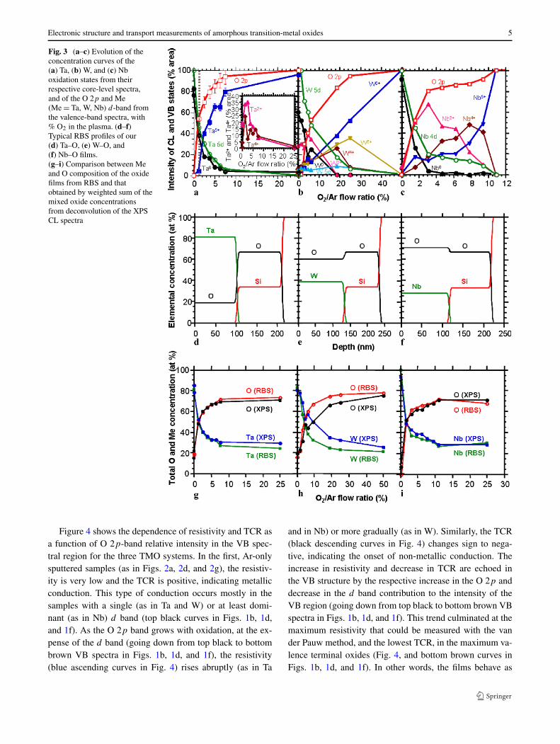
from 80 K to 300 K in 20 steps with equal reciprocal inter-val for the measurements of temperature dependent conduc-tivity. Sample thickness and average composition were ob-tained from Rutherford Backscattering Spectroscopy (RBS,by Evans Analytical Group), which showed a very uniformcomposition profiles throughout the entire films thickness(see Figs. 3d–3f). Good agreement was found between theaverage film composition from RBS and weighted sum of allthe components from deconvolution of the core-level XPSspectra (see Figs. 3g–3i). The layers appeared amorphous inX-ray diffraction (XRD).
3 Core-level (CL) and valence-band (VB) photoelectronspectra
Photoemission is the ideal tool for understanding the chem-ical states in a TMO. The metal element CL peaks in anXPS spectrum are shifted approximately one electron voltto higher binding energy (BE) for every unit increase in theoxidation state of the element, which is well resolved withmodern spectrometers. As examples, the pure metals (ox-idation state 0) display the lowest BE (top black spectra inFigs. 1a, 1c, and 1e) and the terminal highest oxidation statesappear at the highest BE (bottom brown spectra in Figs. 1a,1c, and 1e). All the intermediate valences (oxidation states)appear as features in between the limiting cases. Since theoxidation states for TMO’s (including those of Ta [22–27],W [2–5], and Nb [18, 25]) are known, they can be identi-fied and their concentration quantitatively deconvoluted by
fitting a CL spectral region with various peak models (seeexamples in Fig. 2 and Sect. 2 for details). The above de-scribed oxidation trend is apparent in all three systems, ascan be seen from the dependence of the Ta and W 4f andNb 3d CL photoemission spectra on O2/Ar flow ratio inthe sputtering plasma, shown in Figs. 1a, 1c, and 1e (upperpanel).
From the lower panel of Figs. 1b, 1d, and 1f (lowerpanel), which shows the VB spectra of the three systems,we see that oxidation state also has a profound effect onthe electronic band structure. The VB spectra of the metal-lic samples (top black spectra in Figs. 1b, 1d, and 1f) con-tain a single, relatively narrow, band with a finite densityof states (DOS) at the Fermi level (EF), N(EF), derivedprimarily from the d-orbitals of the transition-metals [28](hereafter “d band”), whereas the fully oxidized terminaloxide states (bottom brown spectra in Figs. 1b, 1d, and 1f)are characterized by a broad binding energy band (5 eV <
�BE < 7 eV) originating from O 2p orbitals (hereafter “2p
band”). The VB intensity, in terms of integrated area un-der the bands, shifts from the d band (100% in the Ar-onlysputtered samples) to the O 2p band, until the d band van-ishes completely in the fully oxidized samples. The O 2p
band, represented by its relative intensity compared to thetotal integrated area of both bands in the VB spectral re-gion, is a good indicator of the degree of oxidation. Simi-larly, the d-band intensity (100% VB intensity—% O 2p-band intensity), is a good indicator of the integrated elec-tron density near EF that participates in the hopping con-duction.
Fig. 1 (a, c, e) Evolution of theTa and W 4f and Nb 3dcore-level spectra, respectively,with % O2 in the plasma.(b, d, f) Respective evolution ofthe valence-band spectra. Thespectra were normalized andsome shifted in BE tocompensate for charging. Fromtop (black) to bottom (brown):sample # 1 (0.00% O2 in theplasma), 2 (Ta–O:1.25%,W–O:1.56%, Nb–O: 1.56% O2),3 (Ta–O: 2.50%, W–O: 3.12%,Nb–O: 3.12% O2), 4 (Ta–O:3.75%, W–O: 4.69%, Nb–O:4.69% O2), 5 (Ta–O: 5.00%,W–O:6.25%, Nb–O: 6.25% O2),6 (Ta–O: 6.25%, W–O: 8.75%,Nb–O: 7.81% O2), 7 (Ta–O:7.50%, W–O: 9.38%, Nb–O:9.38% O2), and 8 (Ta–O:25.00%, W–O: 25.00%, Nb–O:10.90% O2)

4 I. Goldfarb et al.
Fig. 2 Deconvoluted Ta andW 4f and Nb 3d core-levelspectra of the (a, d, g) mostmetallic samples (# 1), (b, e, h)the intermediate samples whereall four doublets were requiredto obtain a good fit, and (c, f, i)the most insulating samples(# 8) fitted almost exclusivelywith a single Ta5+, W+6, andNb+5 doublets, respectively
Figures 3a–3c show the dependence of the oxide filmcomposition on the O2/Ar flow ratio in the Ar–O2 mixedplasma, in terms of the oxidation states found in the threesystems. The quantitative concentration of each state, inatomic percent (at%), was obtained by peak fitting of therespective CL spectra, using peak fitting, as exemplifiedin Fig. 2. Figures 3a–3c also show the variation in rela-tive concentrations of the d and 2p bands, obtained usinga similar routine in the VB region (the sum of these twobands is defined to be 100%). XPS is a surface-sensitivetechnique, with a sampling depth of a few nanometers, andas such does not necessarily represent the composition inthe bulk of the sputtered films throughout their thickness.While the sampling depth can be made deeper using highertakeoff-angle XPS (and our high-angle spectra were no dif-ferent from those in Fig. 1), the sampling depth was stilllimited to no more than 5–10 nm. To avoid concentrationerrors caused by differential yields (common when usingsputter depth profiling), every sample also underwent in-dependent ex situ Rutherford Backscattering Spectroscopy(RBS) analysis, which showed very uniform elemental (Meand O) profiles down to the SiO2/Si substrate (see charac-teristic examples in Figs. 3d–3f). Thus, there is no a priorireason to assume that the composition profiles in terms ofmixed-valence oxidation states should be any different, i.e.,less homogeneous with depth. Furthermore, the RBS pro-files were used to estimate the precision of the quantitativeXPS analysis of the oxidation states. In every sample of eachMe–O system, the total Me and O composition was calcu-lated using the weighted sum of all the metal and oxygenatomic concentrations contained in the mixed oxide states,
and compared with those obtained from RBS. As shown inFigs. 3g–3i, the overlap between RBS and XPS concentra-tion curves was excellent (less than 5% difference), withthe exception of W–O (Fig. 3h), where the higher inaccu-racy of the fitting was most likely caused by the presenceof the 5p transition at BE ∼ 41–42 eV, close to the an-alyzed 4f region. The excellent agreement with RBS re-inforces the robustness and the validity of our XPS dataacquisition and analysis of the film compositions in termsof mixed-valence oxidation states, including the parameterschosen and the constraints imposed on the peak fitting rou-tine.
4 Photoemission and transport
The unoxidized samples represented by the top-black spec-tra in Fig. 1 conform to the classical definition of a metal(conductor), which exhibits partially filled bands with finiteN(EF) and is hence expected to have finite conductivity, σ ,at low temperatures (T → 0) [29]. In contrast, the fully ox-idized samples (i.e., bottom brown spectra in Fig. 1) repre-sent a non-metal (insulator or semiconductor) with all thebands filled and separated by energy gaps, and is hence ex-pected to exhibit zero conductivity as T → 0 [29]. The re-sults of our T -dependent transport measurements, for ex-ample the behavior of the temperature coefficient of resis-tance (TCR) detailed below, fully corroborate these obser-vations, and yield even more interesting findings for themixed-valence samples, characterized by the presence ofboth 2p and d bands.
Electronic structure and transport measurements of amorphous transition-metal oxides 5
Fig. 3 (a–c) Evolution of theconcentration curves of the(a) Ta, (b) W, and (c) Nboxidation states from theirrespective core-level spectra,and of the O 2p and Me(Me = Ta, W, Nb) d-band fromthe valence-band spectra, with% O2 in the plasma. (d–f)Typical RBS profiles of our(d) Ta–O, (e) W–O, and(f) Nb–O films.(g–i) Comparison between Meand O composition of the oxidefilms from RBS and thatobtained by weighted sum of themixed oxide concentrationsfrom deconvolution of the XPSCL spectra
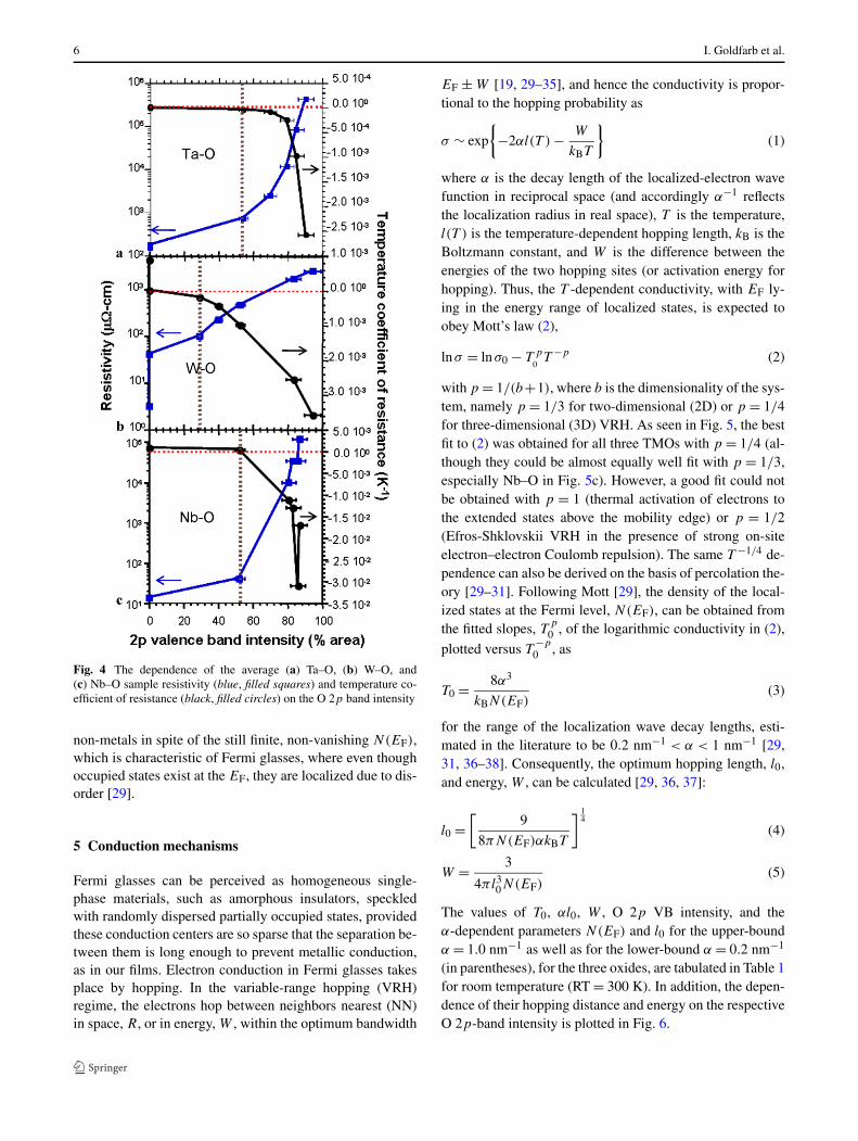
Figure 4 shows the dependence of resistivity and TCR asa function of O 2p-band relative intensity in the VB spec-tral region for the three TMO systems. In the first, Ar-onlysputtered samples (as in Figs. 2a, 2d, and 2g), the resistiv-ity is very low and the TCR is positive, indicating metallicconduction. This type of conduction occurs mostly in thesamples with a single (as in Ta and W) or at least domi-nant (as in Nb) d band (top black curves in Figs. 1b, 1d,and 1f). As the O 2p band grows with oxidation, at the ex-pense of the d band (going down from top black to bottombrown VB spectra in Figs. 1b, 1d, and 1f), the resistivity(blue ascending curves in Fig. 4) rises abruptly (as in Ta
and in Nb) or more gradually (as in W). Similarly, the TCR(black descending curves in Fig. 4) changes sign to nega-tive, indicating the onset of non-metallic conduction. Theincrease in resistivity and decrease in TCR are echoed inthe VB structure by the respective increase in the O 2p anddecrease in the d band contribution to the intensity of theVB region (going down from top black to bottom brown VBspectra in Figs. 1b, 1d, and 1f). This trend culminated at themaximum resistivity that could be measured with the vander Pauw method, and the lowest TCR, in the maximum va-lence terminal oxides (Fig. 4, and bottom brown curves inFigs. 1b, 1d, and 1f). In other words, the films behave as
6 I. Goldfarb et al.
Fig. 4 The dependence of the average (a) Ta–O, (b) W–O, and(c) Nb–O sample resistivity (blue, filled squares) and temperature co-efficient of resistance (black, filled circles) on the O 2p band intensity
non-metals in spite of the still finite, non-vanishing N(EF),which is characteristic of Fermi glasses, where even thoughoccupied states exist at the EF, they are localized due to dis-order [29].
5 Conduction mechanisms
Fermi glasses can be perceived as homogeneous single-phase materials, such as amorphous insulators, speckledwith randomly dispersed partially occupied states, providedthese conduction centers are so sparse that the separation be-tween them is long enough to prevent metallic conduction,as in our films. Electron conduction in Fermi glasses takesplace by hopping. In the variable-range hopping (VRH)regime, the electrons hop between neighbors nearest (NN)in space, R, or in energy, W , within the optimum bandwidth
EF ± W [19, 29–35], and hence the conductivity is propor-tional to the hopping probability as
σ ∼ exp
{−2αl(T ) − W
kBT
}(1)
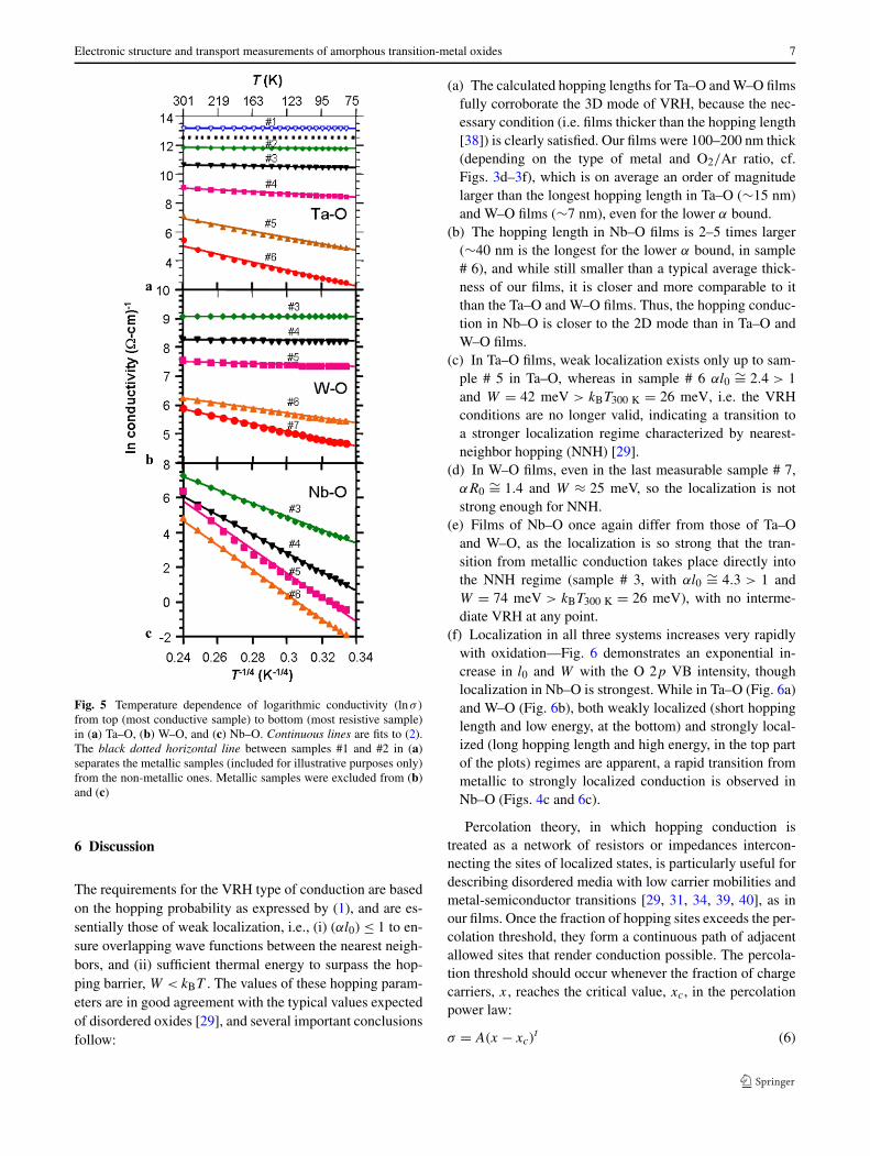
where α is the decay length of the localized-electron wavefunction in reciprocal space (and accordingly α−1 reflectsthe localization radius in real space), T is the temperature,l(T ) is the temperature-dependent hopping length, kB is theBoltzmann constant, and W is the difference between theenergies of the two hopping sites (or activation energy forhopping). Thus, the T -dependent conductivity, with EF ly-ing in the energy range of localized states, is expected toobey Mott’s law (2),
lnσ = lnσ0 − T p0
T −p (2)
with p = 1/(b+1), where b is the dimensionality of the sys-tem, namely p = 1/3 for two-dimensional (2D) or p = 1/4for three-dimensional (3D) VRH. As seen in Fig. 5, the bestfit to (2) was obtained for all three TMOs with p = 1/4 (al-though they could be almost equally well fit with p = 1/3,especially Nb–O in Fig. 5c). However, a good fit could notbe obtained with p = 1 (thermal activation of electrons tothe extended states above the mobility edge) or p = 1/2(Efros-Shklovskii VRH in the presence of strong on-siteelectron–electron Coulomb repulsion). The same T −1/4 de-pendence can also be derived on the basis of percolation the-ory [29–31]. Following Mott [29], the density of the local-ized states at the Fermi level, N(EF), can be obtained fromthe fitted slopes, T
p
0 , of the logarithmic conductivity in (2),
plotted versus T−p
0 , as
T0 = 8α3
kBN(EF)(3)
for the range of the localization wave decay lengths, esti-mated in the literature to be 0.2 nm−1 < α < 1 nm−1 [29,31, 36–38]. Consequently, the optimum hopping length, l0,and energy, W , can be calculated [29, 36, 37]:
l0 =[
9
8πN(EF)αkBT
] 14
(4)
W = 3
4πl30N(EF)
(5)
The values of T0, αl0, W , O 2p VB intensity, and theα-dependent parameters N(EF) and l0 for the upper-boundα = 1.0 nm−1 as well as for the lower-bound α = 0.2 nm−1
(in parentheses), for the three oxides, are tabulated in Table 1for room temperature (RT = 300 K). In addition, the depen-dence of their hopping distance and energy on the respectiveO 2p-band intensity is plotted in Fig. 6.
Electronic structure and transport measurements of amorphous transition-metal oxides 7
Fig. 5 Temperature dependence of logarithmic conductivity (lnσ)
from top (most conductive sample) to bottom (most resistive sample)in (a) Ta–O, (b) W–O, and (c) Nb–O. Continuous lines are fits to (2).The black dotted horizontal line between samples #1 and #2 in (a)separates the metallic samples (included for illustrative purposes only)from the non-metallic ones. Metallic samples were excluded from (b)and (c)
6 Discussion
The requirements for the VRH type of conduction are basedon the hopping probability as expressed by (1), and are es-sentially those of weak localization, i.e., (i) (αl0) ≤ 1 to en-sure overlapping wave functions between the nearest neigh-bors, and (ii) sufficient thermal energy to surpass the hop-ping barrier, W < kBT . The values of these hopping param-eters are in good agreement with the typical values expectedof disordered oxides [29], and several important conclusionsfollow:
(a) The calculated hopping lengths for Ta–O and W–O filmsfully corroborate the 3D mode of VRH, because the nec-essary condition (i.e. films thicker than the hopping length[38]) is clearly satisfied. Our films were 100–200 nm thick(depending on the type of metal and O2/Ar ratio, cf.Figs. 3d–3f), which is on average an order of magnitudelarger than the longest hopping length in Ta–O (∼15 nm)and W–O films (∼7 nm), even for the lower α bound.
(b) The hopping length in Nb–O films is 2–5 times larger(∼40 nm is the longest for the lower α bound, in sample# 6), and while still smaller than a typical average thick-ness of our films, it is closer and more comparable to itthan the Ta–O and W–O films. Thus, the hopping conduc-tion in Nb–O is closer to the 2D mode than in Ta–O andW–O films.
(c) In Ta–O films, weak localization exists only up to sam-ple # 5 in Ta–O, whereas in sample # 6 αl0 ∼= 2.4 > 1and W = 42 meV > kBT300 K = 26 meV, i.e. the VRHconditions are no longer valid, indicating a transition toa stronger localization regime characterized by nearest-neighbor hopping (NNH) [29].
(d) In W–O films, even in the last measurable sample # 7,αR0 ∼= 1.4 and W ≈ 25 meV, so the localization is notstrong enough for NNH.
(e) Films of Nb–O once again differ from those of Ta–Oand W–O, as the localization is so strong that the tran-sition from metallic conduction takes place directly intothe NNH regime (sample # 3, with αl0 ∼= 4.3 > 1 andW = 74 meV > kBT300 K = 26 meV), with no interme-diate VRH at any point.
(f) Localization in all three systems increases very rapidlywith oxidation—Fig. 6 demonstrates an exponential in-crease in l0 and W with the O 2p VB intensity, thoughlocalization in Nb–O is strongest. While in Ta–O (Fig. 6a)and W–O (Fig. 6b), both weakly localized (short hoppinglength and low energy, at the bottom) and strongly local-ized (long hopping length and high energy, in the top partof the plots) regimes are apparent, a rapid transition frommetallic to strongly localized conduction is observed inNb–O (Figs. 4c and 6c).
Percolation theory, in which hopping conduction istreated as a network of resistors or impedances intercon-necting the sites of localized states, is particularly useful fordescribing disordered media with low carrier mobilities andmetal-semiconductor transitions [29, 31, 34, 39, 40], as inour films. Once the fraction of hopping sites exceeds the per-colation threshold, they form a continuous path of adjacentallowed sites that render conduction possible. The percola-tion threshold should occur whenever the fraction of chargecarriers, x, reaches the critical value, xc, in the percolationpower law:
σ = A(x − xc)t (6)

8 I. Goldfarb et al.
Table 1 RT hoppingparameters extracted from theslope of the temperaturedependent conductivity curvesfor the vdP-measurablenon-metallic samples, calculatedwith α = 1.0 nm−1 (0.2 nm−1)
Sample #(Ta–O)
T0 (K) N(EF) (eV−1 cm−3) l0 (nm) αl0 W (meV) 2p (% area)
2 3.34e−01 2.78e+26 (2.22e+24) 0.08 (0.42) 0.08 1.45 54.16
3 1.83e+01 5.08e+24 (4.07e+22) 0.23 (1.14) 0.23 3.95 69.75
4 1.89e+03 4.90e+22 (3.92e+20) 0.73 (3.64) 0.73 12.62 79.45
5 2.33e+05 3.99e+20 (3.19e+18) 2.42 (12.12) 2.42 42.02 84.94
6 6.00e+05 1.55e+20 (1.24e+18) 3.07 (15.36) 3.07 53.24 90.44
7 94.12
8 100.00
Sample #(W–O)
T0 (K) N(EF) (eV−1 cm−3) l0 (nm) αl0 W (meV) 2p (% area)
3 0.16e−01 5.77e+27 (4.61e+25) 0.03 (0.20) 0.03 0.68 29.07
4 6.98e−01 1.33e+26 (1.06e+24) 0.10 (0.51) 0.10 1.74 40.04
5 2.46e+01 3.77e+24 (3.01e+22) 0.25 (1.23) 0.25 4.24 52.55
6 5.60e+03 1.66e+22 (1.33e+20) 0.96 (4.78) 0.96 16.47 83.38
7 2.85e+04 3.26e+21 (2.61e+19) 1.44 (7.18) 1.44 24.74 94.47
8 100.00
Sample #(Nb–O)
T0 (K) N(EF) (eV−1 cm−3) l0 (nm) αl0 W (meV) 2p (% area)
3 2.26e+06 4.11e+19 (3.29e+17) 4.28 (21.40) 4.28 74.17 80.27
4 9.10+06 1.02e+19 (8.16e+16) 6.06 (30.31) 6.06 105.08 83.21
5 2.30e+07 4.03e+18 (3.22e+16) 7.65 (38.23) 7.65 132.53 85.86
6 2.62e+07 3.55e+18 (2.84e+16) 7.89 (39.46) 7.89 136.81 86.87
7 91.45
8 100.00
In the classical models, be it “site percolation” or “bond per-colation” (correlated or otherwise), the NN sites are consid-ered connected, and hence the conductance between sitesdoes not depend on hopping distance or site energy, but israther binary; “1” for the NN sites or “0” for any moredistant neighbors [40]. In this case, regardless of whethersites or bonds are randomly removed from the percolatingmedium, the exponent of the power law is 1.5 < t < 1.6 for3D, and 1.0 < t < 1.3 for 2D, whereas the critical fractionfor 3D site percolation is xc = 0.15 (0.45 for 2D) and for 3Dbond percolation xc = 0.25 (and 0.50 for 2D) [40]. Thesenumbers may vary for modified models in which energy bar-riers for tunneling and hopping, resulting in non-binary con-ductance, are considered [41–43].
This classical description fits well the conductivity trendsof our Ta–O films, as follows from our combined photoe-mission and transport measurements. We assume that the d-band intensity from XPS is proportional to the integrateddensity of occupied states in the VB within W of EF. Inother words, we use the d-band intensity (% area of VBspectra) to represent x in the percolation power law (6), andin Figs. 7a–7c we examine how the conductivity scales with
it. (The actual W within the d band is likely to be narrower,because the latter may include contributions from d-orbitalsof the non-conducting intermediate oxidation states and thefinite resolution of our energy analyzer at RT, however wehave no way of separating those contributions.) The solidblue lines show the best fits of the conductivity data (fromour ex situ T -dependent transport measurements) to the per-colation equation above. The fit for Ta–O (Fig. 7a) yields acritical carrier concentration of about 15%, with the expo-nent of the power law t = 1.5, i.e., in excellent agreementwith the threshold and exponent expected from 3D site per-colation theory [40]. This makes perfect sense, consideringthat in the NNH regime localization is so strong that theprobability of hopping (1) to sites other than the nearest inspace is practically negligible. In other words, the observedconductance is essentially binary, as in the classical perco-lation limit. In Nb–O films (Fig. 7c), the threshold is 17%,very close to Ta–O and to that expected from 3D site per-colation theory. On the other hand, the exponent of ∼1.1 ismore consistent with 2D percolation. This apparently mixed3D–2D percolation mode, mirrors the 3D–2D crossover be-havior already seen in Nb–O in relation to its long hopping

Electronic structure and transport measurements of amorphous transition-metal oxides 9
Fig. 6 (a) Exponential dependence of optimum hopping length(red, open triangles) and energy (blue, open inverted triangles)on the 2p band intensity, fitted with 2.21 × 10⁻³e0.10515x and3.83 × 10−3e0.10515x , respectively (r = 0.9656). (b) and (c) describethe same dependence for W–O and Nb–O samples, respectively. Errorbars reflect experimental uncertainty in the concentration determina-tion. The vertical black dotted line indicates the transition from metal-lic to VRH conduction. Note that in (c) Nb–O does not show the VRHregime at all
lengths and the resulting T -dependence of conductivity be-tween T −1/4 and T −1/3 (see Fig. 5c and the related dis-cussion). Moreover, in the strictest sense, Mott’s law is ex-pected in the VRH regime, whereas NNH is the only hop-ping mechanism found in Nb–O films.
The fit of the W–O conductivity in Fig. 7b is too steep toencompass all the data points, and hence overestimates thepercolation threshold, which should have occurred betweensamples # 7 and # 8, i.e., ∼5%–6% marked by the green linein Fig. 7 and in Table 1. The failure of the simple percolationpower law to predict the conductivity in W–O films is under-standable since the localization conditions are too weak forNNH, and VRH is incompatible with binary conduction.
Fig. 7 (a, b, c) Average conductivity plotted versus the d-band in-tensity for Ta–O, W–O, and Nb–O, respectively. Continuous bluecurve is the best fit using σ = A(I 5d − I 5d
c )m, metal–VRH transi-tion is marked by a vertical blue line, VRH–NNH by vertical redline, and NNH-Percolation threshold by vertical green line. (a) Ta–O:I 5dc = 15.24% ± 4.13%, m = 1.5, (b) W–O: I 5d
c = 34.72% ± 2.16%,m = 1.6, and (c) Nb–O: I 5d
c = 17.02% ± 1.44%, m = 1.1. Note thatthis classical percolation equation does not predict the threshold cor-rectly (red line) for W–O in (b)
The reasons for the differences among the three Me–Osystems originate from their intrinsically different physicalproperties and thermodynamic characteristics. In the Ta–Osystem, TaO and TaO2 phases are only metastable, andtherefore Ta2+ and Ta4+ states disappear very quickly withoxidation (see Fig. 3a), in favor of the only stable Ta5+ va-lence state (Ta2O5 phase). As a result, relations between thecomposition (manifested via CL spectra), the electron bandstructure (manifested via VB spectra), and the actual trans-port properties are relatively simple. For example, Fig. 3aclearly shows that in the absence of the mixed-valence inter-

10 I. Goldfarb et al.
mediates, the VB d band (open circles, green line) is linkeddirectly and primarily to Ta0 states (filled circles, black line),and in the same way the major contributors to the VB 2p
band (open squares, red line) are Ta5+ states (filled squares,blue line). Ta–O is the only one out of the three Me–O sys-tems that clearly exhibits all the distinct regions of varyinglocalization strength, from metallic, through VRH, and thenvia NNH to the percolation threshold. This is not the casewith the other two metal oxides, where intermediate oxi-dation states persist at high concentrations even to the lateoxidation stages (Figs. 3b, 3c).
7 Conclusions
Using X-ray photoelectron spectroscopy and temperature-dependent conductivity measurements, we have studied con-duction mechanisms in reactively sputtered Ta–O, W–O, andNb–O films with varying concentrations of oxygen. Basedon these results we propose a generalized model of conduc-tion in transition-metal oxides, which is presented schemat-ically in Fig. 8. In the metallic state, characterized by a sin-gle Me0 4f or 3d core-level doublet and a single d bandat the Fermi level, the overlap of the electron wave func-tions is sufficient for metallic conduction (Fig. 8a). Oxida-tion causes depletion of the d-band charge carriers in fa-
Fig. 8 Schematic drawing depicting the sequence of the evolvingatomic structure and conduction mechanisms (top panel), and corre-sponding photoemission core-level (middle panel) and valence-band(bottom panel) structure, in amorphous transition-metal oxides incourse of oxidation. The red circles are the localization radii. (a) Un-oxidized metallic state, (b) weakly localized variable range hop-ping regime, (c) more strongly localized nearest-neighbor hopping,(d) strong localization regime on the verge of percolation breakdown,and (e) final highly insulating sub-percolation threshold state
vor of the O 2p valence band, and hence the carrier con-centration decreases until the overlap between wave func-tions is small (i.e., localization is high) enough to inducea transition from metallic to hopping conduction, until, ul-timately, even percolation breaks down. The first (metal–insulator) transition is detected in temperature-dependenttransport measurements by the TCR sign change and in-crease in resistivity (Fig. 4), and, since it is caused by theformation of the first oxides, it can be as easily detectedin XPS by the appearance of the corresponding doublets ofthe mixed-valence oxidation states shifted to higher bind-ing energies in the core-level spectra, and formation of theO 2p valence band (Fig. 8b). Intensity is gradually pumpedfrom the d band into O 2p band with continuous oxidation(Fig. 8c), up to a point where the hopping sites are so sparseand distant from one another that the separation exceedsthe localization radius, and only percolating conduction cantake place (Fig. 8d). Throughout this increasing oxidationprocess, the transport is distinctly non-metallic in spite ofthe finite density of states at the Fermi level (see Fig. 1).These states are Anderson-localized, and the only way con-duction can take place is by electron hopping between them.Our results therefore identify these transition-metal oxidesas Fermi glasses. Ultimately, the separation and localizationincrease so much that the fraction of hopping sites falls be-low the threshold for percolation and the resulting resistivitybecomes too high to measure with a conventional van derPauw method. In photoemission, this transition coincideswith the disappearance of all lower oxidation state core-levelpeaks except the terminal ones at the highest binding energy,and the complete disappearance of the d band at the Fermilevel, with only the O 2p valence band remaining.
The integrated intensity of the d band in the vicinity ofthe Fermi level and of the broad O 2p band were used hereto deduce the relative proportion of the conductive centersin our insulating amorphous films. These integrated intensi-ties can be used as a “critical parameter” for scaling in vari-ous conduction regimes, instead of the normally used carrierdensities, as they effectively represent the integrated densityof states. For example, the degree of localization can be di-rectly assessed from the integrated intensity of the O 2p VB,since both the hopping distance and energy depend expo-nentially on it. The integrated d-band intensity was used asthe critical parameter in the percolation power law and cor-rectly predicted the 3D percolation exponent and thresholdfor Ta–O, and 2D–3D crossover behavior for Nb–O. The re-sults for W–O were less conclusive. In general, both W–Oand Nb–O, with their heterogeneous compositions contain-ing mixed-valence states, showed more complex behaviorthan Ta–O, for which the metastable intermediate oxideswere quick to disappear in favor of the only stable one.
The composition-induced conductivity changes observedhere may provide insight into the material changes within

Electronic structure and transport measurements of amorphous transition-metal oxides 11
oxide-based memristors, for which electrical biasing leadsto oxygen concentration changes in the as-grown “virgin”film within certain conducting channels of the device [44].An electrical bias can dynamically alter the concentration ofoxygen in these channels by moving charged ions (oxygenanions or positive oxygen vacancies), thereby reversibly ex-ploring some portion of the conduction diagram mapped outin Fig. 7, and schematically represented in Fig. 8. For Ta–O,there are four clearly distinct regimes of conduction, metal-lic, three-dimensional weakly localized variable-range andstrongly localized nearest-neighbor hopping, and very highresistivity percolation sub-threshold, which can be attainedby controlling the composition. The more heterogeneouscomposition of metal oxides with more complex phase di-agrams, containing multiple intermediate phases (and henceoxidation states), are likely to have more complicated hop-ping and percolation pathways and barriers, which may bedetrimental to device performance.
Finally, the experimental approach to analyzing the con-duction in amorphous oxide films presented here, based oncombined electronic structure from XPS and transport mea-surements, is both general and rigorous, since it is applica-ble to any compound material system and does not dependon the state of crystallinity of the film.
Acknowledgements This research was supported in part by theSyNAPSE program of the Defense Advanced Research ProjectsAgency under contract HR0011-09-3-0001. The views, opinions,and/or findings contained in this article are those of the authors andshould not be interpreted as representing the official views or poli-cies, either expressed or implied, of the Defense Advanced ResearchProjects Agency or the Department of Defense. The authors gratefullyacknowledge technical assistance of D.A.A. Ohlberg.
References
1. D.W. Bullett, J. Phys. C: Solid State Phys. 16, 2197 (1983)2. K. Mašek, P. Blumentrit, J. Beran, T. Skála, I. Píš, J. Libra, V. Ma-
tolín, Surf. Interface Anal. 42, 540 (2010)3. A. Romanyuk, P. Oelhafren, Sol. Energy Mater. Sol. Cells 84,
1945 (2006)4. L. Weinhardt, M. Blum, M. Bär, C. Heske, B. Cole, B. Marsen,
E.L. Miller, J. Phys. Chem. C 112, 3078 (2008)5. S. Santucci, L. Lozzi, E. Maccallini, M. Passacantando, L. Otta-
viano, J. Vac. Sci. Technol. A 19, 1467 (2001)6. S.-J. Kim, B.J. Cho, M.B. Yu, M.-F. Li, Y.-Z. Xiong, C. Zhu,
A. Chin, D.-L. Kwong, IEEE Electron Device Lett. 26, 625 (2005)7. E. Atanassova, Microelectron. Reliab. 39, 1185 (1999)8. J. Robertson, Eur. Phys. J. Appl. Phys. 28, 265 (2004)9. R. Waser, M. Aono, Nat. Mater. 6, 833 (2007)
10. A. Sawa, Mater. Today 11, 28 (2008)11. D.B. Strukov, G.S. Snider, D.R. Stewart, R.S. Williams, Nature
453, 80 (2008)12. J.J. Yang, M.D. Pickett, X. Li, D.A.A. Ohlberg, D.R. Stewart,
R.S. Williams, Nat. Nanotechnol. 3, 429 (2008)
13. D.S. Shang, L. Shi, J.R. Sun, B.G. Shen, F. Zhuge, R.W. Li,Y.G. Zhao, Appl. Phys. Lett. 96, 072103 (2010)
14. J.P. Strachan, G. Medeiros-Ribeiro, J.J. Yang, M.X. Zhang,F. Miao, I. Goldfarb, V. Holt, M. Rose, R.S. Williams, Appl. Phys.Lett. 98, 242114 (2011)
15. J.J. Yang, M.X. Zhang, J.P. Strachan, F. Miao, M.D. Pickett,R.D. Kelley, G. Medeiros-Ribeiro, R.S. Williams, Appl. Phys.Lett. 97, 232102 (2010)
16. M.-J. Lee, C.B. Lee, D. Lee, S.R. Lee, M. Chang, J.H. Hur,Y.-B. Kim, C.-J. Kim, D.H. Seo, S. Seo, U.-I. Chung, I.-K. Yoo,K. Kim, Nat. Mater. 10, 625 (2011)
17. E.g., see www.springermaterials.com18. M. Grundner, J. Halbritter, J. Appl. Phys. 51, 397 (1979)19. J.M. Honig, L.L. Van Zandt, Annu. Rev. Mater. Sci. 5, 225 (1975)20. S.H. Shin, T. Halpern, P.M. Raccah, J. Appl. Phys. 48, 3150
(1977)21. B. Lalevic, M. Shoga, Thin Solid Films 75, 199 (1981)22. S. Lecuyer, A. Quemerais, G. Jezequel, Surf. Interface Anal. 18,
257 (1992)23. Y. Imai, A. Watanabe, M. Mukaida, K. Osato, T. Tsunoda,
T. Kameyama, K. Fukuda, Thin Solid Films 261, 76 (1995)24. O. Kerrec, D. Devillieres, H. Groult, P. Marcus, Mater. Sci. Eng.
B 55, 134 (1998)25. N.V. Alov, J. Anal. Chem. 60, 431 (2005)26. M. Khanuja, H. Sharma, B.R. Mehta, S.M. Shivaprasad, J. Elec-
tron Spectrosc. Relat. Phenom. 169, 41 (2009)27. V.R.R. Medicherla, S. Majumder, D. Paramanik, S. Varma, J. Elec-
tron Spectrosc. Relat. Phenom. 180, 1 (2010)28. P. Prieto, L. Galan, J.M. Sanz, Appl. Surf. Sci. 70–71, 186 (1993)29. N.F. Mott, E.A. Davies, Electronic Processes in Non-crystalline
Materials (Clarendon, Oxford, 1979)30. H. von Löhneysen, Adv. Solid State Phys. 40, 143 (2000)31. M. Pollak, J. Non-Cryst. Solids 11, 1 (1972)32. M. Imada, A. Fujimori, Y. Tokura, Rev. Mod. Phys. 70, 1039
(1998)33. T. Serin, A. Yildiz, N. Serin, N. Yildirim, F. Özyurt, M. Kasap, J.
Electron. Mater. 39, 1152 (2010)34. L.A. Tracy, E.H. Hwang, K. Eng, G.A. Ten Eyck, E.P. Nordberg,
K. Childs, M.S. Carroll, M.P. Lilly, S. Das Sarma, Phys. Rev. B79, 235307 (2009)
35. T. Ichinohe, S. Masaki, K. Uchida, S. Nozaki, H. Morisaki, ThinSolid Films 466, 27 (2004)
36. R. Shabna, P.M. Sarun, S. Vinu, U. Syamaprasad, J. AlloysCompd. 481, 797 (2009)
37. Z.H. Khan, M.M. Malik, M. Zulfequar, M. Husain, J. Phys., Con-dens. Matter 7, 8979 (1995)
38. K.G. Lisunov, B. Raquet, H. Rakoto, J.M. Broto, E. Arushanov,X.Z. Xu, H. El Alami, C. Deville Cavellin, J. Appl. Phys. 94, 5912(2003)
39. K.M. Itoh, E.E. Haller, J.W. Beeman, W.L. Hansen, J. Emes,L.A. Reichertz, E. Kreysa, T. Shutt, A. Cummings, W. Stockwell,B. Sadoulet, J. Muto, J.W. Farmer, V.I. Ozhogin, Phys. Rev. Lett.77, 4058 (1996)
40. S. Kirkpatrick, Rev. Mod. Phys. 45, 574 (1973)41. L.J. Huijbregts, H.B. Brom, J.C.M. Brokken-Zijp, W.E. Kleinjan,
M.A.J. Michels, Phys. Rev. B 77, 075322 (2008)42. B. Sixou, J.P. Travers, C. Barthet, M. Guglielmi, Phys. Rev. B 56,
4604 (1997)43. D. Toker, D. Azulay, N. Shimoni, I. Balberg, O. Millo, Phys. Rev.
B 68, 041403(R) (2003)44. F. Miao, W. Yi, I. Goldfarb, J. Joshua Yang, M.-X. Zhang,
M.D. Pickett, J.P. Strachan, G. Medeiros-Ribeiro, R. StanleyWilliams, ACS Nano (2012, in press). doi:10.1021/nn2044577