Embed Size (px)
Citation preview

Electronic and Magnetic Structure of Transition Metals
doped GaN
Seung-Cheol Lee, Kwang-Ryeol Lee, Kyu-Hwan LeeFuture Technology Research Division, KIST, Korea

Spintronics and Spin FETSpintronics and Spin FET
D. Awschalom et al, Scientific American (2002)
Spin Field Effect Transistor
• Semiconductor based device
•Conceptually, spin FET is similar to conventional FET.
•Charges of FET are controlled by induced bias voltage, while spins of electrons are controlled in spin FET.
•To do so, spin injection is the first step to realize spin FET.
•Find an effective material that can inject spin into the gate.
Control of Spin and Charge of Electrons Simultaneously

Diluted Magnetic SemiconductorsDiluted Magnetic Semiconductors Diluted Magnetic Semoconductor (DMS)
- A ferromagnetic material that can be made by doping of impurities, especially transition metal elements, into a semiconductor host.
- Conducting spin polarized carriers of DMS are used for spin manipulation.
- Compatible with current semiconductor industry.
Spin Field Effect Transistor

Success and Failure of Ga1-xMnxAsSuccess and Failure of Ga1-xMnxAs
• Mn substitutes Ga in zincblende structure– Structure is compatible
with GaAs 2DEG
• Tc is correlated with carrier density
• Ferromagnetic semiconductor with ordering temperature ~ 160 K
• Finding a new DMS material having high Tc
Ku et al., APL 82 2302 (2003)
Mn

Motivation: DMSs beyond Ga1-xMnxAsMotivation: DMSs beyond Ga1-xMnxAs
T. Dietl, Semicond. Sci. Technol. 17 (2002) 377
What will happen if other transition elements are used as dopants?

Requirements for Successful DMSRequirements for Successful DMS
TMTM
Local Moments and Splitting Valence Bands Simultaneously

Transition Element(V, Cr, Mn, Fe, Co,
Ni and Cu)
1st NN Nitrogen 4th Nitrogen
2nd NN Nitrogen 3rd NN Nitrogen
Which TM is Feasible in GaN Host?Which TM is Feasible in GaN Host?
5th Nitrogen
Design Rule: Finding a TM that induces spin polarization of valence band
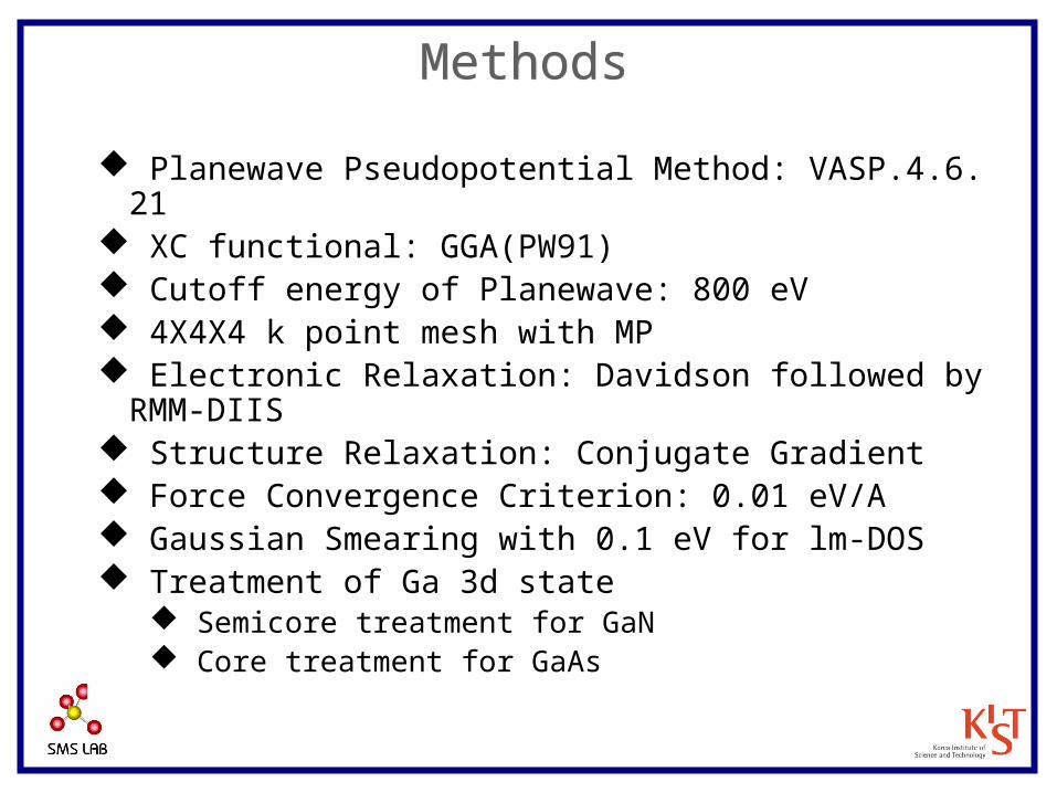
Planewave Pseudopotential Method: VASP.4.6.21 XC functional: GGA(PW91) Cutoff energy of Planewave: 800 eV 4X4X4 k point mesh with MP Electronic Relaxation: Davidson followed by RMM-DIIS Structure Relaxation: Conjugate Gradient Force Convergence Criterion: 0.01 eV/A Gaussian Smearing with 0.1 eV for lm-DOS Treatment of Ga 3d state
Semicore treatment for GaN Core treatment for GaAs
MethodsMethods

As stateTotal DOS and Mn d state*10
Example: Electronic Structure of GaMnAsExample: Electronic Structure of GaMnAs
Localized Moment due to MnDelocalized Carrier
due to p-d Exchange Interaction

More-than Half filled
Total and Local Magnetic MomentsTotal and Local Magnetic MomentsLess-Than Half filled

Spin Density of TM doped GaN Spin Density of TM doped GaN
Less-Than Half filled
More-than Half filled
GaN:Cr GaN:Mn
GaN:Co GaN:Cu

More-than Half filled
Total and Local Magnetic MomentsTotal and Local Magnetic MomentsLess-Than Half filled

GaFeN: Magnetic Insulator GaCoN: Half Metal
GaNiN: Magnetic Insulator GaCuN: Half Metal
Partial DOSs having More-Than Half Filled StatesPartial DOSs having More-Than Half Filled States

Up Spin Down SpinUp SpinUp Spin
t2g
eg
Filled Electron Unfilled Electron
Up Spin Down SpinUp SpinUp Spin
GaN:Mn(7)-half metal GaN:Co(9)-half metal
Up Spin Down SpinUp SpinUp Spin
GaN:Ni(10)-insulator
Up Spin Down SpinUp SpinUp Spin
GaN:Cu(11)-half metal
Electron Occupation in GaNElectron Occupation in GaNNo
Splitting of Valence p-
band
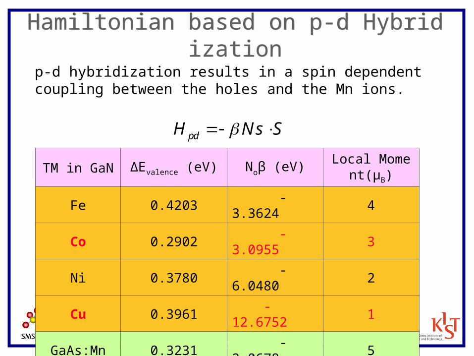
Hamiltonian based on p-d HybridizationHamiltonian based on p-d Hybridizationp-d hybridization results in a spin dependent coupling between the holes and the Mn ions.
pdH Ns S
TM in GaN ΔEvalence (eV) Noβ (eV)Local
Moment(μB)
Fe 0.4203 -3.3624 4
Co 0.2902 -3.0955 3
Ni 0.3780 -6.0480 2
Cu 0.3961 -12.6752 1
GaAs:Mn 0.3231 -2.0678 5
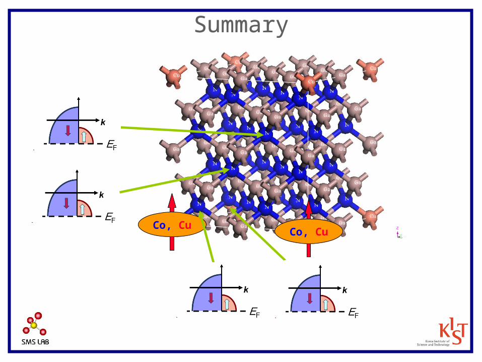
SummarySummary
Co, CuCo, Cu


![Smoothly Varying Affine Stitching [CVPR 2011] Ph.D. Student, Chang-Ryeol Lee February 10, 2013](https://img.dokumen.tips/doc/110x75/5697bfb81a28abf838c9f0a8/smoothly-varying-affine-stitching-cvpr-2011-phd-student-chang-ryeol-lee.jpg)


![100+ Times Faster Weighted Median Filter [cvpr ‘14] Presenter: Chang-Ryeol Lee](https://img.dokumen.tips/doc/110x75/56649d705503460f94a52b92/100-times-faster-weighted-median-filter-cvpr-14-presenter-chang-ryeol.jpg)


