Embed Size (px)
Citation preview

Electron Energy Loss Spectroscopy
R. K. Zheng School of Physics, the University of Sydney, Sydney, NSW 2006, Australia
Keywords: Electron Energy Loss Spectroscopy; Transmission Electron Microscopy
1. Introduction
When a specimen is exposed to a nearly monochromatic electron beam, due to the Coulomb interaction with the atoms (both electrons and nuclei) in the specimen, some of the electrons in the beam will undergo inelastic scattering, lose certain energy and have their trajectories slightly and randomly deflected.1-3 The energy loss of each electron and therefore the energy loss spectrum of all the electrons in the incident beam will then be measured through an electron spectrometer. The measured spectrum is electron energy loss spectrum, and the technique is electron energy loss spectroscopy (EELS).4-6 Since energy is conserved in the beam-specimen system, the lost energy of beam electrons must be transferred to the atoms of the specimen and radiated out in form of electromagnetic wave. Therefore, the characteristic spectrum of the material can be deduced from EELS.7 EELS was originally proposed and demonstrated by Hillier and Baker in 1944,8 but was not widely used until it got more widespread in research in the 1990s owing to advances in microscope instrumentation and spectroscopy technology.4-6 The technique has obtained spatial resolutions down to ~0.1 nm by employing modern aberration-corrected probe forming, while the energy resolution can be 100 meV (milli-electron Volts) or better with a monochromatic electron source and careful deconvolution.9, 10 This has enabled detailed measurements of the electronic structures and materials properties of single columns of atoms, and in a few cases, of single atoms. EELS can be classified into transmission EELS and reflection EELS (REELS) by the geometry. In REELS,11 a specimen is bombarded with a focused low energy (<30 keV) electron beam and the energy loss spectrum of the reflected electrons is measured. REELS spectrum contains features corresponding to discrete energy losses of the reflected electrons due to excitation of vibrational and plasmon states and provides information on the type and geometric structure of atoms and molecules at the surface of the specimen. If much lower energy (0.1–1 keV) electron beams are adopted for REELS, the energy dispersion of the beam can be reduced to meV via a monochromator and similar energy resolution could be achieved.12 This technique is therefore referred to as high-resolution EELS (HREELS) and used to study the vibrational motion of atoms and molecules on and near the specimen surface.5, 11 Probably the most commonly used is transmission EELS,4-6 in which most of incident electrons pass through the specimen and energy loss is measured. Transmission EELS is usually equipped with a transmission electron microscope (TEM) or scanning transmission electron microscope (STEM), in which kinetic energy of incident electrons is typically 100 to 300 keV (kilo-electron Volts). Thus, the analytical capabilities of EELS are combined with the high spatial resolution probe of TEM.13 There are also dedicated transmission EELS systems designed for the purpose of extreme high energy at the expense of spatial resolution.10, 14, 15 This review will be devoted to transmission EELS, and hereafter, the term of EELS will be dedicated to transmission EELS. This review is organized as follows: following this Introduction, Section 2 briefs the physics of EELS; Section 3 is devoted to the instrumentation and experimental aspects of EELS; Section 4 covers the processing of EELS spectrum; Section 5 focuses on the quantification of EELS spectrum; Section 6 discusses the imaging techniques of EELS; Section 7 gives an example of the applications of EELS to spintronic materials; Finally, EELS is compared with relative techniques and concluded.
2. Physics of Electron Energy Loss Spectroscopy
2.1 Electronic Structure of Atoms and Solids
EELS originates from the interactions between incident beam and atoms (especially electrons) in the specimen,1-3 and therefore carries the characteristics of the materials in the specimen. It is valuable to recall the electronic structure of atoms and solids first. In classical physics, electrons were thought to orbit around atomic nuclei, much like the planets around the sun. In quantum mechanics, atomic orbitals are described by wave functions over space, indexed by n (principle quantum number), l (orbital angular quantum number), m (magnetic quantum number), and s (spin quantum number). Shells and subshells are defined by principle and angular quantum number, respectively. The shell names K, L, M, N… denote n=1, 2, 3, 4…, respectively. The subshell names (s, p, d, f, g, h ...) are derived from the quality of their spectroscopic
Microscopy and imaging science: practical approaches to applied research and education (A. Méndez-Vilas, Ed.)
545
___________________________________________________________________________________________

lines: sharp, principal, diffuse and fundamental, the rest being named in alphabetical order.16 Figure 1 shows the orbitals in the shells and subshells of an atom. Shown on the right is the orbital name in form of nXj, where n is the principle quantum number, X is the subshell names (s, p, d, f, g, h ...), and j is total angular quantum number. Shown on the bottom is the corresponding edge names used in spectroscopy.17
Figure 1. Electron configuration in atoms. States of electrons and edges in spectrum are given in the right and bottom. After Ahn & Krivanek.17 The electrons of a single free-standing atom occupy atomic orbitals in form of discrete energy levels. If several atoms are brought together to form a molecule, their atomic orbitals will split like in a coupled oscillation, as shown in Figure 2. This produces a number of molecular orbitals proportional to the number of atoms. When a large number of atoms are brought together to form a solid, the number of orbitals becomes so large, and the difference in energy between them becomes so small as not to be indistinct. As a result, discrete energy levels in atoms become energy bands in solids,18 as shown in Figure 2. However, some intervals of energy contain no orbitals, no matter how many atoms are aggregated, which is called band gap. Above the band gap is the conduction band; below it is called valence band. Electron energy levels in a solid is described by band structure, which determines many physical properties, in particular its electronic and optical properties, of a material.18
Figure 2. Energy levels split when atoms are brought together and finally form energy band structure in solids.
Microscopy and imaging science: practical approaches to applied research and education (A. Méndez-Vilas, Ed.)
546
___________________________________________________________________________________________
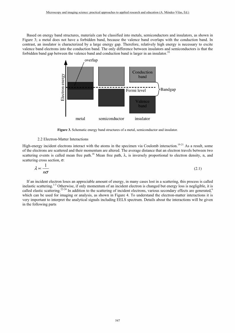
Based on energy band structures, materials can be classified into metals, semiconductors and insulators, as shown in Figure 3; a metal does not have a forbidden band, because the valence band overlaps with the conduction band. In contrast, an insulator is characterized by a large energy gap. Therefore, relatively high energy is necessary to excite valence band electrons into the conduction band. The only difference between insulators and semiconductors is that the forbidden band gap between the valence band and conduction band is larger in an insulator.18
Figure 3. Schematic energy band structures of a metal, semiconductor and insulator.
2.2 Electron-Matter Interactions
High-energy incident electrons interact with the atoms in the specimen via Coulomb interaction.19-21 As a result, some of the electrons are scattered and their momentum are altered. The average distance that an electron travels between two scattering events is called mean free path.18 Mean free path, λ, is inversely proportional to electron density, n, and scattering cross section, σ:
1
nλ
σ∝ (2.1)
If an incident electron loses an appreciable amount of energy, in many cases lost in a scattering, this process is called inelastic scattering.1-3 Otherwise, if only momentum of an incident electron is changed but energy loss is negligible, it is called elastic scattering.22-24 In addition to the scattering of incident electrons, various secondary effects are generated,6 which can be used for imaging or analysis, as shown in Figure 4. To understand the electron-matter interactions it is very important to interpret the analytical signals including EELS spectrum. Details about the interactions will be given in the following parts
Microscopy and imaging science: practical approaches to applied research and education (A. Méndez-Vilas, Ed.)
547
___________________________________________________________________________________________

Figure 4. Electron-specimen interactions and secondary effects in a TEM.
2.3 Elastic Scattering
In the case of elastic scattering, the electrons interact with the Coulomb potential of atomic nuclei, which deviates the trajectory of incident electrons without any appreciable energy loss.25 In fact, a small energy loss occurs since the nuclei are moved by the impact. However, because of the disparity in mass of the scattered electron and the constituent atom, the loss is too small to affect the coherency of the beam. Elastic scattering is the main component of the scattering process in the case of high-energy incident electrons such as in TEM. As shown in Figure 5, although some incident electrons undergo Rutherford high-angle scattering, even backscattering, most of them are only scattered by a small-angle (<100 mrad),5 because nuclei are tiny compared to atoms and their potential decreases quickly due to inverse-square law and the screen of electrons. Small-angle elastic scattering are usually coherent so that elastically scattered electrons form diffraction.
Figure 5. Elastic scattering of incident electron by the Coulomb potential of atomic cores.
Microscopy and imaging science: practical approaches to applied research and education (A. Méndez-Vilas, Ed.)
548
___________________________________________________________________________________________
2.4 Inelastic Scattering
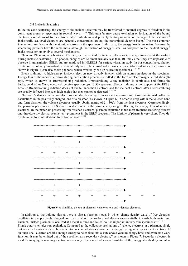
In the inelastic scattering, the energy of the incident electron may be transferred to internal degrees of freedom in the constituent atoms or specimen in several ways.1-3, 23 This transfer may cause excitation or ionization of the bound electrons, excitations of free electrons, lattice vibrations and possibly heating or radiation damage of the specimen.6 Inelastically scattered electrons are generally concentrated around the transmitted electron beam.6 The most common interactions are those with the atomic electrons in the specimen. In this case, the energy loss is important, because the interacting particles have the same mass, although the fraction of energy is small as compared to the incident energy.7 Inelastic scattering involves several mechanisms. Phonons: Phonons, or vibrations of lattice, can be excited by incident electrons inside specimens or at the surface during inelastic scattering. The phonon energies are so small (usually less than 100 meV) that they are impossible to observe in transmission EELS, but are employed in HREELS for surface vibration study. In our context here, phonon excitation is not very important because it only has to be considered at low energies. Absorbed incident electrons, as shown in Figure 4, can also excite phonons, which eventually end up as heat in specimens.6, 26, 27 Bremsstrahlung: A high-energy incident electron may directly interact with an atomic nucleus in the specimen. Energy loss of the incident electron during deceleration process is emitted in the form of electromagnetic radiation (X-ray), which is known as Bremsstrahlung radiation. Bremsstrahlung X-ray radiation is continuous and forms the background of an X-ray energy dispersive spectroscopy (EDS) spectrum. Bremsstrahlung is not important for EELS, because Bremsstrahlung radiation does not excite inner-shell electrons and the incident electrons after Bremsstrahlung are usually deflected into such high angles that they cannot be detected.6, 28, 29 Plasmon: Valence/conduction electrons can absorb energy from incident electrons and form longitudinal collective oscillations in the positively charged ions or a plasmon, as shown in Figure 6. In order to keep within the valence band and form plasmon, the valence electrons usually obtain energy of 5 - 30eV from incident electrons. Correspondingly, the plasmon peak in an EELS spectrum distributes in the same energy range reflecting the energy loss of incident electrons. In the materials possessing free valence electrons, plasmon excitation is the most frequent scattering process and therefore the plasma peak is very prominent in the EELS spectrum. The lifetime of plasma is very short. They de-excite in the form of interband transition or heat.5, 30-32
Figure 6. A simplified picture of plasmon: + denotes ions and - denotes electrons. In addition to the volume plasma there is also a plasmon mode, in which charge density wave of free electrons oscillates in the positively charged ion matrix along the surface and decays exponentially towards both metal and vacuum. Surface plasmon is localized at a metal surface and called, so it is important in very thin specimens.5, 33, 34 Single outer-shell electron excitation: Compared to the collective oscillations of valence electrons in a plasmon, single outer-shell electrons can also be excited to unoccupied states above Fermi energy by high-energy incident electrons. If an outer-shell electron absorbs enough energy to be excited into a state above vacuum energy level and overcome work function, it may be emitted out of the specimen as a secondary electron,35 as shown in Figure 7. Secondary electron is used for imaging in scanning electron microscopy. In a semiconductor or insulator, if the energy absorbed by an outer-
Microscopy and imaging science: practical approaches to applied research and education (A. Méndez-Vilas, Ed.)
549
___________________________________________________________________________________________

shell electron is larger than the energy gap and not enough to escape, the electron may transit to the conduction band. This process is known as interband transition,36, 37 as shown in Figure 7. In a metal without energy gap, the situation is different. Electron-hole pairs38 can be created with small energy by lifting an electron from an energy level below the Fermi energy to a level above. In the de-excitation process of excited outer-shell electrons, the energy may be released in the form of cathodoluminescence or heat.39, 40 Single inner-shell electron excitation: Single inner-shell electrons can also be excited into unoccupied states via the interaction with incident electrons, although their ground energies are usually hundreds or thousands of eV lower than Fermi energy. In order to excite a single electron, the incident electron must transfer energy equal to or larger than the binding energy of an electron in the specimen, and therefore carries the characteristic of the binding energy.41, 42 The low energy vacancy left by an excited inner-shell electron will be re-occupied quickly by another electron at a higher energy state. In this de-excitation process, the excess energy will be released as electromagnetic wave (X-ray in this case) that is used in X-ray EDS,43, 44 or the excess energy will be absorbed by a third electron that may be emitted as an Auger electron,45 as shown in Figure 7.
Figure 7. Schematic energy band structure of a material (NiO) showing inner shell (K, L), valence band and conduction band, Fermi energy (EF), and vacuum energy (Evac). Primary processes including inner shell and outer shell excitations are shown in the left. Secondary effects including Auger electrons emission and photons radiation are shown in the right. After Egerton5 and Kundmann.46
2.5 Single, Plural, and Multiple Scattering
Electron scattering can also being categorised as single, plural, and multiple scattering according to the times of electrons being scattered (inelastically or elastically).5 If an incident high-energy electron is scattered only one time, it undergoes a single scatter. If the specimen is thin compared to the mean free path, most of the scattering is single scattering. If the inelastic mean free path for outer-shell excitation can be comparable to the specimen thickness, the EELS spectrum may contain an appreciable contribution from electrons which have been scattered more than once. This is known as plural scattering, in which lower loss scattering results in the pre-edge background and produces a mixed core-loss signal.47 As a result, the plural-scattering component changes the shape of the spectrum and may obscure characteristic peaks or edges. It can be removed by deconvolution, to yield a single-scattering distribution which is independent of the specimen thickness.48 If the thickness of a specimen is much larger than mean free path, incident electrons undergo multiple scattering.49, 50 In this case, individual peaks disappear in the EELS spectrum and is difficult to interpret.5 Provided electron scatterings are individual events, the probability to observe n-folder scattering follows Poisson distribution.5
1
!n m
nP m en
−= (2.2)
Microscopy and imaging science: practical approaches to applied research and education (A. Méndez-Vilas, Ed.)
550
___________________________________________________________________________________________

where m is the mean number of scattering times. In EELS, m is determined by inelastic mean free path λi and specimen thickness:
i
tm
λ= (2.3)
which is also referred as scattering parameters.5
2.6 Formulation of Scattering
The precise description of the scattering process needs to be done in the framework of quantum mechanics. Figure 8
shows the wave vector diagram of inelastic scattering.22-24 An incident electron with a wave vector of ik
(energy
( )22i i eE k m= ) inelastically scattered by atoms in the specimen, loses momentum of ( )i jq k k= −
(energy
( )2 2 2 2i j eE k k mΔ = − ) and is deflected by an angle of θ. In this inelastic scattering process, the atomic electron
in the specimen is excited from initial state |i′ > to final state |f ′ > (the prime symbol added to distinguish the
constituent atomic electron from the incident beam electron). The transition rate, or probability of transition per unit time, from the initial state |i′ > to the final state |f ′ > is described by Fermi’s Golden Rule.51 The probability, or the
differential cross section, of the incident electron undergoing this scattering is given by Bethe theory:52-54
( )2
2
2 40
4| exp |i f f
i
d kf iq r i
d a q k
σ γ′ ′ ′ ′= < ⋅ >Ω
(2.4)
where 2 sind dπ θ θΩ = is the differential of solid angle, 2 21 1- v cγ = is the relativistic factor,
20 0a 0.053 nmeh e mε= = is the Bohr radius. The term in the bra-ket is the transition-matrix ( ),M q E
.
( ) ( ), , | exp |i fM q E f iq r i′ ′ ′ ′=< ⋅ > (2.5)
The square of the magnitude of the transition-matrix is known as inelastic form factor or dynamical structure factor.5 The generalized oscillator strength (GOS) is defined as:
( ) ( )2,, ,4 2
0
, ,i ji f i f
Ef q E M q E
Ra q′ ′
′ ′ ′ ′= (2.6)
where ,i jE ′ ′ is the excitation energy or the energy loss of the incident electron, and 4 2 208 13.6 eVeR m e hε= = is
the Rydberg energy. In most typical cases, the final sate is not a single eigenstate, but a continuum of states, such as the conduction band. The above equation needs to be differentiated upon the excitation energy E.5
( )2 2
2
,4 j
i
k df q Ed R
d dE Eq k dE
σ γ=Ω
(2.7)
In EELS, the energy loss is very small compared to the high energy of incident electrons E (Ei or Ej), and scattering
angle is very small too. In this case, jk can taken to be equal to ik , and
( )2 2 2 2i Eq k θ θ= + (2.8)
where θ is the characteristic angle of the scattering.
20
E
E
m vθ
γ= (2.9)
The double differential cross section can then be written as
Microscopy and imaging science: practical approaches to applied research and education (A. Méndez-Vilas, Ed.)
551
___________________________________________________________________________________________

( )2 220
2 2 2
,8 1
e E
df q Ea Rd
d dE Em v dE
σθ θ
=Ω +
(2.10)
At small scattering angles, the angular dependence is from the Lorenzian factor 2 21 Eθ θ+ .5 The exponential term
( )exp iq r⋅ can be expanded as series:
( )exp 1 ...iq r iq r⋅ = + ⋅ + (2.11)
Because the eigenstates |i′< and |f ′ > are orthogonal to each other, the first term turns out to be 0 in the transition-
matrix. In cases of small scattering angle and small energy loss, the higher power term can be neglected and only the iq r⋅
term needs to be considered. Consequently, the double differential cross section is simplified as:
( ) 2,, 4
0
, | |i ji j
Ef q E f r i
Ra′ ′
′ ′ ′ ′= < > (2.12)
Dipolar selection rule, which limits the transition to 1lΔ = ± and 1,0 ±=Δj , is applicable in this case, just as in
X-ray absorption spectroscopy.6
Figure 8. Wave vector diagram of inelastic scattering, where ki and kf are the wave vector of the beam electron before and after
scattering, q= ki-kj is the change of wave vector or q is momentum transferred to the specimen.
An alternative approach to derive the scattering cross section is to use the wave vector and frequency dependent
dielectric constant of a material, ( ),qε ω .7, 55 It is well known that, in the Maxwell's equations, all the materials-
related properties are included in the dielectric constant and magnetic permeability. In non-magnetic materials the latter can be ignored. The differential cross section for inelastic scattering is expressed approximately as:
( )2
2 2 20
1 1 1Im
,e E
d
d dE a m v N q E
σπ ε θ θ
−≈ Ω + (2.13)
where N is the atom density of the specific element in the material, ( )Im 1 ,q Eε − is the imaginary part of the
dielectric constant, which is known as the energy–loss function and completely describes the response of the materials to the inelastic scattering.5
ki
kf
θ
q
Microscopy and imaging science: practical approaches to applied research and education (A. Méndez-Vilas, Ed.)
552
___________________________________________________________________________________________

3. Instrumentation and Experimental Aspects
3.1 Instrumentation
Transmission EELS is usually installed on a TEM or scanning transmission electron microscope (STEM).5, 13 A TEM is composed of the illumination system (above specimen), imaging system (below specimen), and recording system, as shown in Figure 9. The illumination system includes the electron gun that emits electrons, accelerator that gives electrons kinetic energy, and condenser lens that tune electrons to a desirable electron beam. The imaging system includes objective, intermediate, and projector lens that generate images or diffraction patterns. The recording devices are films or CCD camera.56 Figure 9 shows schematic diagrams of a TEM working in imaging and diffraction modes respectively. In imaging mode, electron beams are focused by condenser lens onto the specimen; electrons passing through the specimen are focused by the objective lens to form an image called the first intermediate image; this first intermediate image forms a virtual object for the next lens, the intermediate lens, which produces a magnified image of it called the second intermediate image; in turn, this second intermediate image becomes the virtual object for the projector lens; the projector lens forms the greatly-magnified final image on the viewing screen of the microscope. In imaging mode, electrons that emerge from the same point in the specimen are brought together again at the same point in the final image. At the back focal plane of the objective lens, electrons that have left the specimen at different points, but at the same angle, are brought together and form a diffraction pattern. The diffraction pattern that is formed at the back focal plane of the objective lens becomes the virtual object for the lens behind. Finally, a magnified diffraction pattern is projected on the viewing screen of the TEM by weakening the intermediate lens to place the microscope in diffraction mode.24, 56, 57
Figure 9. Electron ray diagrams of TEM in imaging and diffraction modes respectively. Solid arrows and broken lines indicate images and diffraction planes respectively. The resolution δ of a TEM depends on the electron wavelength (acceleration voltage) and the quality of the
objective lens SC :24, 56
Microscopy and imaging science: practical approaches to applied research and education (A. Méndez-Vilas, Ed.)
553
___________________________________________________________________________________________

3 4 1 4SCδ λ= (3.1)
So there are two choices to improve the resolution: either to use the low λ (highest acceleration voltage), or a
low SC . For a medium-voltage TEM (200-300 kV), the lowest commercially available values of SC are ~ 0.5 mm.
TEM has been heavily used in both physical science and the biological sciences.24, 56 Figure 10 shows a JEOL JEM 3000F TEM with a GIF (Gatan Imaging Filter).
Figure 10. A JEOL 3000F TEM with a GIF A TEM can be a modified STEM by introducing scanning coils and suitable detectors.24, 56 There are also dedicated STEM such as VG HB601UX STEM with Gatan Enfina EELS spectrometer shown in Figure 11. In a STEM, electrons emitted from the gun form into a fine beam down to sub-nanometer58 and are focused on a specimen by the objective lens. The scanning coil rasters the fine beam across the thin specimen and passing electrons form an image of the specimen. The images are produced a spot at a time, as in the scanning electron microscope, rather than all at one time as in the TEM. Atom-sized electron beams could be created in an electron microscope equipped with a high brightness field emission electron gun. Using beam energies of 100-300 KeV, the structure and chemistry at sub-nanometer can be examined with various associate techniques: bright field imaging using small angle elastic scattering; high angle annular dark field (HAADF) using large angle elastic scattering; EELS using small angle inelastic scattering; and EDS using characteristic X-ray production etc. The practical STEM was first built by Albert Crewe in the late 1960’s at the University of Chicago.59 Figure 11 shows the schematic electron ray diagram in a VG HB601UX STEM with Gatan Enfina EELS spectrometer. Magnified diagram of an electron beam before and after interacting with a specimen is shown in Figure 12.
Microscopy and imaging science: practical approaches to applied research and education (A. Méndez-Vilas, Ed.)
554
___________________________________________________________________________________________

Figure 11. A VG HB601UX STEM with Gatan Enfina EELS spectrometer. A schematic electron ray diagram is also shown. 15 Courtesy of M. Bosman
Figure 12. Electron ray diagrams of STEM for EELS measurements.
α
β
Specimen
Objective Aperture
Collector Aperture
EELS Entrance Aperture
Microscopy and imaging science: practical approaches to applied research and education (A. Méndez-Vilas, Ed.)
555
___________________________________________________________________________________________

Figure 13. Schematic diagram of a post-column spectrometer. After Mike Kundmann.46 In EELS, an electron spectrometer is used to disperse the energy distribution in the electrons. There are two types of electron spectrometers: in-column Ω filter and post-column spectrometer.5 The latter is more popular and will be considered here. As shown in Figure 13, with lifting the viewing screen, the electrons from the TEM or STEM enter the EELS spectrometer through the entrance aperture situated just below the viewing screen. The conjugate plane of the energy-dispersive plane in the spectrometer is the back focal plane of the projective lens. In other words, the virtual object of the spectrometer lens is the diffraction (in imaging mode) image (in diffraction mode) at the back focal plane of the projective lens. In the EELS spectrometer, electrons are deflected through 90 ° by a magnetic prism and dispersed onto a detector in accordance with their energies.57 The energy dispersion of EELS spectrometer is about 2 μm/eV for 100 kV electrons.5 The energy resolution, which is defined as the full width at half maximum (FWHM) of zero loss peak (ZLP), depends on both TEM/STEM and EELS spectrometer. VG HB601UX STEM with cold emission gun and Gatan Enfina EELS spectrometer can provide an energy resolution of 0.25 eV.15
3.2 Experimental Parameters
The technique of EELS is characterized by its energy resolution and spatial resolution. Energy resolution of 0.1 eV has been achieved on a transmission electron microscope equipped with a monochromator and a high-resolution imaging filter.60 FEI Titan 80-300 TEM with a monochromator and an aberration corrector yields atomic-scale imaging with resolution below 0.6 Angstrom. On the other side, a 300 kV VG Microscope HB603U STEM equipped with a Nion aberration corrector reach spatial resolution down to 0.6 Angstrom. The new record of 0.5 Angstrom is achieved by using transmission electron aberration-corrected microscope.61 In order to obtain high quality EELS spectra, the experimental parameters must be optimized. The energy resolution depends on the electron source, lens in TEM/STEM and EELS spectrometer, the electron detector in the EELS spectrometer, and environmental factors. The energy dispersion of EELS spectrometer and detector sensitivity have effects on the energy resolution. Environmental electromagnetic effect should also be minimized. The electron source probably is the most important single factor affecting energy resolution.62, 63 Electron sources always have an energy spread due to the fermion nature of electrons and electrons emission process. In thermionic sources, the energy spread is determined by Maxwell-Boltzmann statistics at the temperature of the cathode and is typically in the order of 0.5 eV, often increased by electron-electron interactions. The energy spread of Schottky emitters, now used widely in advanced microscopes, is 0.4 to 0.8 eV, depending on the extraction field and thus on the brightness of the source. Cold field emission guns have the narrowest energy spread, which can be as narrow as 0.18 eV at low extraction fields. But to achieve reasonable brightness and signal/noise ratio (SNR), a higher extraction field is
High Loss Zero Loss
Microscopy and imaging science: practical approaches to applied research and education (A. Méndez-Vilas, Ed.)
556
___________________________________________________________________________________________
needed and the energy spread becomes around 0.3 eV.6 The energy spread could be significantly reduced by introducing monochromators, but at the expense of lower brightness and SNR. Post-column electron spectrometers are used in most transmission EELS systems. After being emitted from a specimen, electrons must also pass through the imaging lenses in a TEM before entering an EELS spectrometer. At high energy loss, chromatic aberration effects could be very severe.64 First, at the object plane of the spectrometer lens, which usually corresponds to the projector-lens crossover, chromatic and spherical aberrations blur the diffraction (in imaging mode) or image (in diffraction mode). Consequently the image or diffraction at spectrometer image plane is also blurred and therefore the energy resolution is degraded. Secondly, at the TEM screen or the EELS entrance aperture just below, aberrations broaden the image or diffraction pattern. If the broadness is large enough, some of the electrons (most probably the energy lost electrons) are blocked by the EELS entrance aperture. This effect will vary at different ionization edges, so it may lead to an error in the measurement of scattering cross sections and quantifications of EELS spectrum.5 One important experimental parameter is the collection angle, β, which limit the scattering angle of electrons to be analysed, as indicated in Figure 12. In STEM, the collection angle is usually defined by collector aperture or EELS entrance aperture, and camera length in case of no collector aperture. The convergence angle of the incident beam α (usually 2-10 mrad),65 as shown in Figure 12, is defined by objective lens in STEM. The collection angle should be at least two times that of the convenience angle, in order to fulfil Poisson distribution of scattering angles, because a Poisson distribution is assumed in scattering formulism.5 In TEM, the collection angle limitation is a little complicated and dependent on the working modes. In imaging mode, TEM and EELS lens are coupled via the diffraction at the back focal plane of projector lens, which is also the front focal plane of EELS lens at the same time. In this case, the objective aperture controls the collection angle, while the analysed area of a specimen is selected by the EELS entrance aperture, as show in Figure 9. In diffraction mode, the image at the back focal plane of projector lens is the virtual object to image. The collection angle is controlled by the EELS entrance aperture and the camera lens, while the analysed area is limited by selected area aperture or incident beam.6 Because different electron scattering processes have different scattering angle, the collection angle is an important experimental parameter influencing SNR, signal/background ratio (SBR) quantification, and sensitivity of the EELS data.65 Spatial resolution of EELS in a TEM depends on the working modes. In imaging mode, an analysed area is selected by and spatial resolution is determined by EELS entrance aperture.5 However, at large energy losses the chromatic aberration of the objective lens introduces contributions from object regions outside of the selected area. The offset is typically100 nm.13 The imaging mode is suitable for recording EELS spectra with large collection angle and high energy resolution, but the spatial resolution is only moderate. In diffraction mode the analysed area is selected, and therefore the spatial resolution is determined by the beam diameter. The effects of chromatic aberration are not so severe as in imaging mode. A modern TEM with field emission gun is already able to focus beam diameter down to sub-nanometer, so diffraction mode is suitable for the highest spatial resolution EELS. In a STEM, electron beam size as low as 0.2 nm is used. Because there are no post-specimen lenses in most dedicated STEMs, the aberrations of post-specimen lenses are well excluded. Therefore, dedicated STEMs such as VG microscopes have the privilege of both energy and spatial resolutions.
3.3 Specimen Aspects
Sufficiently thin specimens are critical to avoid excessive multiple scattering in EELS measurements, so therefore the projected thickness of a specimen should be less than one mean free path, λ, in inelastic scattering. Mean free path depends on the kinetic energy of incident electrons and the materials of the specimen. For 100 kV electrons, it is about 120 nm for carbon, 110 nm for silicon, 75 nm for copper and 55 nm for gold.5 Although multiple scattering can be deconvoluted in single scattering, adverse effects are also introduced. The optimal specimen thickness for maximum SNR is determined by the inelastic and elastic mean free paths, λi and λe:
2e i
i e
tλ λλ λ
=+
(3.2)
In many cases, inelastic and elastic mean free paths are not every different, the optimal thickness is about one third of the mean free path.55 Contaminations could be very serious during EELS experiments.66 Contaminations are usually hydrocarbon that may be migrated and deposited on the analysed area. This does not only bring unwanted signals and backgrounds, but also rapidly increases the thickness of a specimen. Specimens must be kept free from hydrocarbon at every stage of preparation and storage. Specimens may be pre-cleaned with plasma or other methods before are loaded into TEM/STEM. During experiments, the use of cold finger or specimen stage could trap contaminations. If hydrocarbon contaminations take place, a large dose of electron beam could be spread on the whole specimen to re-deposit the hydrocarbon on a large area and form a much thinner uniform film.6 In addition to hydrocarbon contaminations, oxidization could also be a serious problem given the EELS specimen is very thin. For example, a monolayer of oxygen
Microscopy and imaging science: practical approaches to applied research and education (A. Méndez-Vilas, Ed.)
557
___________________________________________________________________________________________

on a 20 nm thick sample may constitute 10% to 20% of the sample volume and of course many materials of interest oxidize rapidly in air. For this reason STEM instruments are often provided with an ultra-high vacuum chamber, in which specimens may be prepared and transferred quickly into microscopes. The radiation damage to the specimen induced by the electron beam could be severe, since high-dose and high-energy electrons are directed on a tiny area. Generally, metals are highly resistant to beam damage due to the nature of metallic bond. Inorganic insulators are more sensitive than metals and organic materials, and ionic crystals are very sensitive to beam damage. Knock-on damage is most severe for light elements and hydrogen is easily driven out of many samples.57
3.4 Detector Backgrounds
The electrons passing through electron spectrometer are finally detected by charge couple diode (CCD) camera. The electron-hole pairs in CCD induced by thermal excitation always cause noise readout, even without illumination. This is called dark noise. Since CCD dark current is dependant upon temperature, CCD must reach its set target temperature before acquiring the dark reference image. The dark count is best measured without an electron beam immediately prior to or after data acquisition using the same acquisition parameters as the data.15 Another artefact from the detector is the difference of individual CCD in responding to a uniform illumination over the whole CCD array, because some CCDs generate more electron-hole pair than others. This is called gain variation.67 These gain variations from one channel to another give rise to both high frequency and low frequency artefacts in a spectrum. There are a number of different approaches to correcting these channel-to-channel gain variations. The simplest approach is to remove the specimen from field of view and evenly spread the illumination across the whole CCD array by a broad undispersed beam, and the resultant gain-normalization spectrum is divided into the spectra as a gain reference.65 The gain variation can then be removed by subtracting the gain reference from a spectrum. It is important to prepare a new gain reference image after the CCD has reached the equilibrium temperature (normally about 1-2 hours). The gain reference image should be checked daily.68
4. Processing of Electron Energy Loss Spectra
4.1 Components of an Electron Energy Loss Spectrum
After losing energy via a range of inelastic scattering with atoms in the specimen, incident electrons with different energies are dispersed through an electron spectrometer, just as light is dispersed by a prism, and form an electron energy loss spectrum, as shown in Figure 14. A typical EELS spectrum is shown below. It consists of three parts:6, 7
Figure 14. Relationships between EELS spectrum of the incident electrons and excitations of inner-shell and outer-shell electrons in the specimen. After Mike Kundmann.46
ZLP
Plasmon
L3 L2
Microscopy and imaging science: practical approaches to applied research and education (A. Méndez-Vilas, Ed.)
558
___________________________________________________________________________________________

(ZLP) at 0 eV, as shown in Figure 14, consists of the incident electrons that have lost no energy or small losses owing to phonon scattering on their way passing through the specimen, i.e. they have only interacted elastically or do not interact with the specimen at all. Width of the zero-loss peak reflects energy spread of the electron source and is usually used to align EELS spectrometers. Although ZLP does not possess useful information about electronic energy structure of the material in a specimen, the relative height of ZLP reflects the thickness of the specimen.69 Low-loss region (<75 eV), as shown in Figure 14, reflects the outer-shell electron excitations, such as plasmon oscillations and interband transitions. Since the plasmon generation is the most frequent inelastic interaction for the materials with weakly bound, quasi-free electrons, the intensity in this region is relatively high. Intensity and number of plasmon peaks increases with specimen thickness. Interband transitions occurring in insulators and semiconductors also lie in this region.6 High-loss region (>75 eV), as shown in Figure 14, reflects the inner-shell electron excitations or core losses. Compared to the outer-shell electron excitations, the inner-shell ionization is a much less probable process; as a result, intensity of the core loss peaks are much lower. A minimum energy equal to binding energy of the inner-shell electron is needed for the ionization of the electron. At this energy the scattering cross-section reaches its maximum. Higher energy can also ionize the electron, but the scattering cross-section decreases with increasing the energy. Therefore, intensity of the absorption edge decreases with increasing energy loss and core losses features edges.4 In the high-loss region, the amount of inelastically scattered electrons drastically decreases with increasing energy loss, thus small peaks are superimposed on a strongly decreasing background. There are also considerable amounts of detailed fine structure around core-loss edges: Energy Loss Near Edge Structure (ELNES) and Extended Energy Loss Fine Structure (EXELFS). ELNES in shape of peaks appears at 30-40 eV above the threshold of the core-loss edge, while EXELFS features oscillations in intensity following ELNES.6 High-loss fine structures, which cannot be observed in atoms, arise from the electronic band structure of solids.70
4.2 Removal of Background
All energy loss edges lie on a background composed of the tails of preceding edges including plasmon peak and any ionisation edges with lower threshold energies, as well as the Bremsstrahlung X-ray. This relatively large background is one of the major disadvantages of EELS, making weak edges difficult to see and analyse. A small collection angle β will increase SBR, at the expense of SNR. In the high-loss region there is an approximately linear dependence between the logarithm of the intensity and the logarithm of the energy loss. This log-log relationship means that the background can therefore be fitted using a power law function.71 In general, the power-law background model is the most robust and gives the most reasonable fit for typical EELS edge data. However, if an edge is in the low-loss region below about 100 eV, or if another edge precedes it closely, then the simple power-law model will likely fail. In this case, a polynomial or log polynomial model function will give better results.72, 73
Figure 15. An example of background removal by power law fitting using DigitalMicrograph. The light grey and dark grey filled curves are measured and background removed spectra, respectively. The pre-edge fitting region and fitted curve are also shown.
Microscopy and imaging science: practical approaches to applied research and education (A. Méndez-Vilas, Ed.)
559
___________________________________________________________________________________________

Another method is to use difference spectra. In this method, two spectra, offset in energy by a few eV, are taken. The background can be removed using a first-difference approach (which is equivalent to differentiating the spectra) by subtracting one from the other. This is the only way to remove the background if the specimen thickness changes over the area of analysis. The difference spectra method can also suppress spectral artefacts, particularly the channel-to-channel gain variation.
4.3 Extraction of Zero-Loss Peak
Zero-loss peak is usually very strong in intensity. It also has a tail extending to low-loss region and even further due to the spread of the electron source and phonon scattering. Zero-loss peak must be extracted in order to observe and interpret a low-loss spectrum. Zero-loss peak can be measured by moving the specimen of the field of view in the same conditions as in data spectrum measurement. The data spectrum is subtracted by the measured zero-loss peak and zero-loss peak extracted spectrum is thus obtained. If the separate zero-loss peak is not or is not able to be recorded, zero-loss peak can be fit with several models.74 Reflected tail model is fast, robust and well suited to the majority of cases, and therefore is recommended for general use. Because the tail of the zero-loss peak can contain a substantial number of counts related to the loss part of the spectrum, it is important to take them into account when performing the zero-loss peak extraction. In reflected tail model, this is achieved by assuming the zero-loss tails are relatively symmetric and uses a reflection of the left-side tail to model the tail on the energy-loss side. Figure 16 shows a low-loss spectrum before and after zero-loss peak removal with reflected tail model. The low-loss features are clearly resolved after zero-loss peak extraction.68
Figure 16. A low-loss spectrum before (shown in light grey fill) and after (shown in dark grey fill) zero-loss peak (shown in line) extraction using DigitalMicrograph. Fitted log tail model simply fits and extrapolates zero-loss peak with a logarithmic. Since the model is relatively simple, and the fitting range may be user specified, it is both robust and versatile. A few more models are available including Gaussian- Lorenzian and Maxwell-Boltmann fit.
4.4 Removal of Plural Scattering
If the thickness of the specimen is comparable with mean free path, the probability of plural scattering process increases. More than one core-loss excitation by one incident electron is rare, but a core-loss excitation plus low-loss excitation indeed occur. Lower loss scattering results in the pre-edge background and produces a mixed core-loss signal. As a result, the plural-scattering component changes the shape of the spectrum and may obscure characteristic peaks or edges. Plural scattering leads to a redistribution of counts within the spectrum according to the probability distribution represented by the shape of the low-loss part of the spectrum. Provided scattering is independent events,
Microscopy and imaging science: practical approaches to applied research and education (A. Méndez-Vilas, Ed.)
560
___________________________________________________________________________________________
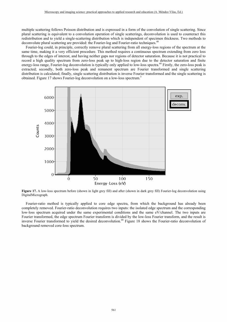
multiple scattering follows Poisson distribution and is expressed in a form of the convolution of single scattering. Since plural scattering is equivalent to a convolution operation of single scatterings, deconvolution is used to counteract this redistribution and to yield a single-scattering distribution which is independent of specimen thickness. Two methods to deconvolute plural scattering are provided: the Fourier-log and Fourier-ratio techniques.48 Fourier-log could, in principle, correctly remove plural scattering from all energy-loss regions of the spectrum at the same time, making it a very efficient procedure. This method requires a continuous spectrum extending from zero loss through to the edges of interest, and having neither gaps nor regions of detector saturation. Because it is not practical to record a high quality spectrum from zero-loss peak up to high-loss region due to the detector saturation and finite energy-loss range, Fourier-log deconvolution is typically only applied to low-loss spectra.68 Firstly, the zero-loss peak is extracted; secondly, both zero-loss peak and remanent spectrum are Fourier transformed and single scattering distribution is calculated; finally, single scattering distribution is inverse Fourier transformed and the single scattering is obtained. Figure 17 shows Fourier-log deconvolution on a low-loss spectrum.5
Figure 17. A low-loss spectrum before (shown in light grey fill) and after (shown in dark grey fill) Fourier-log deconvolution using DigitalMicrograph. Fourier-ratio method is typically applied to core edge spectra, from which the background has already been completely removed. Fourier-ratio deconvolution requires two inputs: the isolated edge spectrum and the corresponding low-loss spectrum acquired under the same experimental conditions and the same eV/channel. The two inputs are Fourier transformed, the edge spectrum Fourier transform is divided by the low-loss Fourier transform, and the result is inverse Fourier transformed to yield the desired deconvolution.68 Figure 18 shows the Fourier-ratio deconvolution of background removed core-loss spectrum.
Microscopy and imaging science: practical approaches to applied research and education (A. Méndez-Vilas, Ed.)
561
___________________________________________________________________________________________

Figure 18. The Fourier-ratio deconvolution (in light grey fill in front) of background removed core-loss spectrum (in dark grey fill) shown in Figure 15 using DigitalMicrograph. Only after artefacts correction, background removal and deconvolution of plural scattering, quantitative analysis can be carried out.
5. Quantification of Electron Energy Loss Spectra
EELS is able to provide information on the elemental composition, crystal structure, and electronic structure. In this section the applications of EELS spectrum will be covered, as shown in the table below. EELS imaging techniques will be covered in the next section. Table 1. Summary of analytical applications of EELS. after Brydson6 and Egerton.5
Spectral region Applications Low-loss or full spectrum Specimen thickness Low-loss: Plasmon peak position Valence electron density; Phase identification Low-loss: Plasmon peak shift Alloy composition Low-loss: Surface plasmon Surface/interface state Low-loss: Interband transition Band gap Low-loss: Fine structure Joint density of states (JDOS) Core-loss: Edge intensities Elemental analysis Core-loss: Orientation dependence Atom site location Core-loss: Chemical shift of edges Oxidization state, valency Core-loss: L or M white line ratio Magnetic moment, valency Core-loss: ELNES Unoccupied projected density of states (PDOS) Core-loss: ELNES Element-specific local coordination, valency Core-loss: EXELFS Elemental specific radial distribution
5.1 Specimen Thickness
As the specimen thickness increases, the probability of inelastic scattering increases, and these events follow a Poisson distribution. In an EELS spectrum, Poisson distribution Pn means the ratio of the energy integrated intensity In of n-folder scattering to the total integrated intensity It:
5
Microscopy and imaging science: practical approaches to applied research and education (A. Méndez-Vilas, Ed.)
562
___________________________________________________________________________________________

1
!i
n t
nn
t i
I tP e
I nλ
λ−
= =
(5.1)
For example, n=0 means zero-loss peak.
0
ln t
i
It
Iλ= (5.2)
Eq.(5.2) gives a measure of the local thickness in a specimen.75-77 The accuracy of the thickness determination is influenced by a number of experimental parameters: zero-loss peak must not be saturated; zero-loss peak must be modelled accurately for effective separation from the loss part of the spectrum; the probed specimen area must be of uniform thickness; the low-loss spectrum should be acquired up to a suitable energy (generally 200eV), at which the extrapolated power law used to correct for truncation of the spectrum may be assumed to be valid; and the collection angle must be large enough (generally 5-10 mrad) so that the plural scattering obeys Poisson statistics.68 For example, from the zero-loss peak and the remanent loss spectrum shown in Figure 16, the thickness of the specimen is around 0.5λ or 40 nm.
5.2 Plasmon Peak
Plasmon peak, which usually dominates the low-loss region, is the resonant oscillation of valence electrons in response to interaction with incident beam. The volume plasmon energy Ep in the free-electron model is expressed as:31
2
0p
e
neE
m ε=
(5.3)
where n is the valence electron density, ε0 is the permittivity in vacuum. The plasmon excitation is coupled to the interband transitions in insulators and semiconductors. The two processes are not independent, so the intensity is not the simple sum of the individuals, and the plasmon peak position are also shifted. Since all the electrons have a binding energy equal to and larger than the band gap Eg, the plasmon peak is approximately given by:5
2 2 2,p i p gE E E= + (5.4)
Because valence electrons are nearly free, the free electron model works very well in most cases. Knowing the effective mass, the valence electron density can be deduced from the above equations. Otherwise, given the valence electron density, the above equation provides a way to calculate effective mass.78, 79 The shift of the plasmon peak indicates the changes in electronic structure, especially the valence electron density and its effective mass. It is known that some materials, such as aluminium and magnesium, produce sharp plasmon peaks. These materials in a specimen can be identified by the sharp plasmon peak.5, 80 The width of the plasmon peak is usually a few eV and reflects the lifetime of plasmon. On the other hand, plasmon energy depends on the moment transfer q
, which is known as plasmon dispersion:5
( )2
2p p
e
E q E qm
α= + (5.5)
where α is the dispersion coefficient. This relation reveals the asymmetric shape of plasmon peak with an extended tail on the high-energy side, especially for large collection angle β, which means that the electrons of large q
are collected
in the EELS. There is a cut-off momentum transfer beyond which single electron excitation occurs and collective plasmon disappears.70
5.3 Surface Plasmon Peak
Surface plasmon is apparent in thin films, nanowires, and nanoparticles, which have a large aspect ratio and therefore have enhanced surface effect. In the free electron model, the energy of surface plasmon is related to volume plasmon by:
Microscopy and imaging science: practical approaches to applied research and education (A. Méndez-Vilas, Ed.)
563
___________________________________________________________________________________________

2s pE E= (5.6)
It shows that the surface plasmon peak is lower than volume plasmon in an EELS spectrum.5 Because nanomaterials have a large aspect ratio, surface plasmon are usually observed and provides a previous method to access the electronic structure, especially valence electron density at sub-nanometer scale.81-83 In the examples shown in Figure 19, surface plasmon peaks of EELS were used to image localized optical excitations with sufficient resolution to reveal the dramatic spatial variation over one single nanoparticle. So far no experimental technique is competent for this type of work.84
Figure 19. STEM–EELS measurements on an equilateral Ag nanoprism with 78-nm-long sides. Left: HAADF–STEM image of the particle, showing the regular geometry. Right: A series of 32 successive low-loss EELS spectra acquired along an axis (A to B) of the nanoprism.84 Copyright Nature Publishing Group. Reproduced with permission.
5.4 Interband Transition Peaks
In addition to the plasmon peaks, interband transitions may also appear in the low-loss region as peaks superimposed on the plasmon peaks. Interband transition is single electron excitation from valence band to unoccupied conduction band, where either the initial state or final state is single discrete.85, 86 Therefore, the cross section expressions given in
Section 0 need to be convoluted by the density of states in valence band ( )v Eρ and density of unoccupied states in
conduction band ( )c Eρ .
( ) ( ) ( )2
, v v
dq E E E E dE dEd
d dE
σσ ρ ρ′ ′ ′= + ΩΩ (5.7)
which reflects the so-called joint density of states (JDOS) – a convolution of valence and conduction band DOS.6 In order to facilitate interband transition, a constituent atomic electron must absorb the energy at least equal to the band gap. This provides a way to measure the band gap, which is associated with the initial rise in intensity in low-loss EELS spectrum. Figure 20 shows the magnified low-loss part of Figure 16 or Figure 17. It is clear to see the onset of intensity at 3.6 eV, which is consistent with the reported value of band gap.87
Microscopy and imaging science: practical approaches to applied research and education (A. Méndez-Vilas, Ed.)
564
___________________________________________________________________________________________
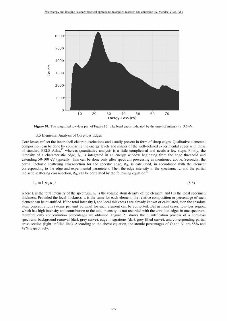
Figure 20. The magnified low-loss part of Figure 16. The band gap is indicated by the onset of intensity at 3.6 eV.
5.5 Elemental Analysis of Core-loss Edges
Core losses reflect the inner-shell electron excitations and usually present in form of sharp edges. Qualitative elemental composition can be done by comparing the energy levels and shapes of the well-defined experimental edges with those of standard EELS Atlas,17 whereas quantitative analysis is a little complicated and needs a few steps. Firstly, the intensity of a characteristic edge, IX, is integrated in an energy window beginning from the edge threshold and extending 50-100 eV typically. This can be done only after spectrum processing as mentioned above. Secondly, the partial inelastic scattering cross-section for the specific edge, σX, is calculated, in accordance with the element corresponding to the edge and experimental parameters. Then the edge intensity in the spectrum, IX, and the partial inelastic scattering cross-section, σX, can be correlated by the following equation:6
X t XI I Xn tσ= (5.8)
where It is the total intensity of the spectrum, nX is the volume atom density of the element, and t is the local specimen thickness. Provided the local thickness, t, is the same for each element, the relative composition or percentage of each element can be quantified. If the total intensity It and local thickness t are already known or calculated, then the absolute atom concentrations (atoms per unit volume) for each element can be computed. But in most cases, low-loss region, which has high intensity and contribution to the total intensity, is not recorded with the core-loss edges in one spectrum, therefore only concentration percentages are obtained. Figure 21 shows the quantification process of a core-loss spectrum: background removal (dark grey curve), edge integrations (dark grey filled curve), and corresponding partial cross section (light unfilled line). According to the above equation, the atomic percentages of O and Ni are 58% and 42% respectively.
Microscopy and imaging science: practical approaches to applied research and education (A. Méndez-Vilas, Ed.)
565
___________________________________________________________________________________________

Figure 21. Quantification of a core-loss spectrum using DigitalMicrograph. The measured spectrum and core-loss edges are shown in light-grey filled and dark-grey filled curves, respectively. The cross sections and background are shown in light grey and dark grey lines.
5.6 Energy Loss Near Edge Structure
ELNES reflects the influence of the atoms surrounding the excited atom and requires bank structure explanation. Provided the excitation of one inner shell electron has no effect on the other atomic electrons, according to Fermi’s Golden Rule, the transition rate, or scattering cross section in EELS σ, is proportional to the square of transition matrix
( )2M E and density of final states ( )N E :5
( ) ( )2dM E N E
dE
σ ∝ (5.9)
( )M E governs the overlap between initial state |i′ > to final state |f ′ > , and therefore determines the basic
position and shape of the edges. ( )N E represents the local, unoccupied, density of states available for the transition
happening, and leads to the ELNES. If dipolar approximation applies, the non-zero ( )M E is limited to 1lΔ = ± . In
this case, ( )N E only represents the angular moment-projected density of states (PDOS). Therefore, ELNES directly
reflects local, unoccupied PDOS, as shown in Figure 22.
Microscopy and imaging science: practical approaches to applied research and education (A. Méndez-Vilas, Ed.)
566
___________________________________________________________________________________________

Figure 22. Schematic diagram showing the relationship between ELNES and PDOS.
The unoccupied PDOS and the initial inner-shell state could be modified by the ambient bonds and atoms due to the changes in chemistry, valency, and/or crystal structure. Therefore, ELNES provides an approach for the qualitative or quantitative analysis on the chemistry, valency, and crystal structure. Firstly, if the surrounding atoms of an atom are changed with different element(s), consequently the binding energy between them will be modified and the related edges will be shifted, which is known as chemical shift.88 The shift in effect is similar to those observed in other spectroscopy, such as X-ray photoemission spectroscopy.6 An excellent example was shown by Aushterlonie et al in blind experiments on a range of amorphous materials in which silicon is bonded to various ligands (B, C, N, O and P).89 The different ligands are accurate and rapidly identified according to the two ELNES features of the Si-L edge spectra examined: the overall shape and the energy position. It was found that the shift of the first Si L-edge is proportional to the electronegativity of the surrounding ligands, as shown in Figure 23.
0.0 0.2 0.4 0.6 0.8 1.0 1.2 1.4 1.6
0
1
2
3
4
5
6
7
8
O
N
C
Ene
rgy
Shi
ft (e
V)
Electronegtivity (eV)
BP
Figure 23. The electronegativity dependence of the energy shift (relative to a-Si) of the first peak in the Si-L edge spectra. After
Aushterlonie.89
E
N(E)
Filled StateEmpty State
Microscopy and imaging science: practical approaches to applied research and education (A. Méndez-Vilas, Ed.)
567
___________________________________________________________________________________________

Secondly, the valency of an atom can also change the initial core-level state and final state, and therefore the position and shape of ELNES. In L2,3 edges of 3d and 4d transition metals and M4,5 edges of rare earth elements, the effect is very clear due to the strong interaction between core hole and excited electron. Because the final states lie in the narrow d or f bands, the L2,3 edges and M4,5 edges display very sharp intensity known as white lines.6 The white lines are well separated due to the spin-orbital splitting of, for example, 2p orbitals in 3d transition metals. L2 edge comes from the lower energy level and therefore appears at higher energy side in an EELS spectrum. Garvie et al has shown that valence-specific multiplet structures can be used as valence fingerprints, as shown in Figure 24.90 The following were investigated: Mn L2,3 from a range of manganese oxides, including manganosite (MnO: Mn2+), ganophyllite ((K,Ca,Na)2(Fe,Mn)8(Si,Al)12O29(OH)7⋅nH2O: Mn2+), bixbyite ((Mn,Fe)2O3: two distinct Mn3+ sites), norrishite (KLiMn4Si8O24: single Mn3+ site), asbolan (Mn(O,OH)2(Co,Ni)x(OH)2x⋅nH,O: Mn4+), and ramsdellite (MnO2: Mn4+). In general, the edges exhibit a chemical shift toward higher energy losses with the increase of valency. At the same time, the ratio of the intensity of L2 and L3 edges also shows the clear dependence on the valency of the excited atom. Although the energy level splitting of the spin-orbital coupling in the initial core states is responsible for the separation of the L2 and L3 edges, their intensity ratio actually reflects the final unoccupied density of states of different spins according to Pauli Exclusion Principle. Therefore, the occupancy of the final states (3d bands of transition metals, or 4f bands of rare earth elements) can be deduced. This can not only provide information on valency but also on the atomic magnetic moment.5, 6
Figure 24. Mn L2,3 edges from a range of Mn compounds showing the effect of different valency on the shape and position of the L2,3.
90 Copyright Mineralogical Society of America. Reproduced with permission. Thirdly, even if the valency of an excited atom or the chemistry of surrounding atoms is kept unchanged, the electronic structure, or the bond, can be affected by the change in crystal structure. In general, only the atoms in the first coordination shell have significant effect on the excitation of the centre atom. Thus ELNES provides a means to qualitatively determine the nearest neighbour coordination, known as coordination fingerprints.91, 92 For example, Figure 25 shows the carbon K-edges of diamond, graphite, and the fullerene C60. The edge of graphite consists of an
Microscopy and imaging science: practical approaches to applied research and education (A. Méndez-Vilas, Ed.)
568
___________________________________________________________________________________________

initial sharp peak at ~285 eV and a second broad peak at ~290 eV. These features may be attributed to transitions from 1s to the unoccupied π* and σ* molecular orbitals.90 C60 has the similar carbon K-edge shapes to graphite but with differences due to its molecular nature. Diamond has a different edge shape from them, with only one peak maximum at ~293 eV. The differences between the carbon K edges in graphite and diamond may be explained by the sp2 bonding in graphite and sp3 bonding in diamond. The sp2 bonding results in a peak at 285 eV due to transitions to the π* orbitals, and a second peak at 290 eV due to transitions to σ* orbitals. Because sp3 bonding of diamond is, in fact, tetrahedrally directed hybrid orbitals, the only peak of diamond is identified as arising from transitions to σ* molecular orbitals.90
Figure 25. Carbon K edges of graphite, diamond and C60.93 Courtesy of Kurata.
5.7 Extended Energy Loss Fine Structure
Although the intensity of ELNES decreases with increasing energy loss in an EELS spectrum, the oscillation of the intensity is still observable over hundreds of eV if no other edges follow.94, 95 The extended oscillation of the intensity in fine structure is known as extended energy loss fine structure (EXELFS) – analogue to the extended X-ray absorption fine structure (EXAFS). EXAFS originates from the interaction between the excited electron and its long-range neighbouring atoms. The excited electron is ejected with energy ε and behaves as a wave with a wave vector
2 ek m ε= . This outgoing spherical wave is reflected from neighbouring atoms, as shown in Figure 26. The
outgoing wave and the reflected waves interact and form interference, which can be constructive or destructive. Consequently the final state and transition rate of the excited electron is also influenced. Therefore, the oscillation of intensity, i.e. EXELFS, could be observed in an EELS spectrum in many cases. The oscillating component is very sensitive to the numbers of atoms Nj in the neighbouring shell j. Nj is called radial distribution function (RDF), which can be deduced from Fourier analysis of EXELFS. A large energy range of typically a few hundred eV is needed to obtain adequate EXELFS data, which seriously limits its application.
Microscopy and imaging science: practical approaches to applied research and education (A. Méndez-Vilas, Ed.)
569
___________________________________________________________________________________________
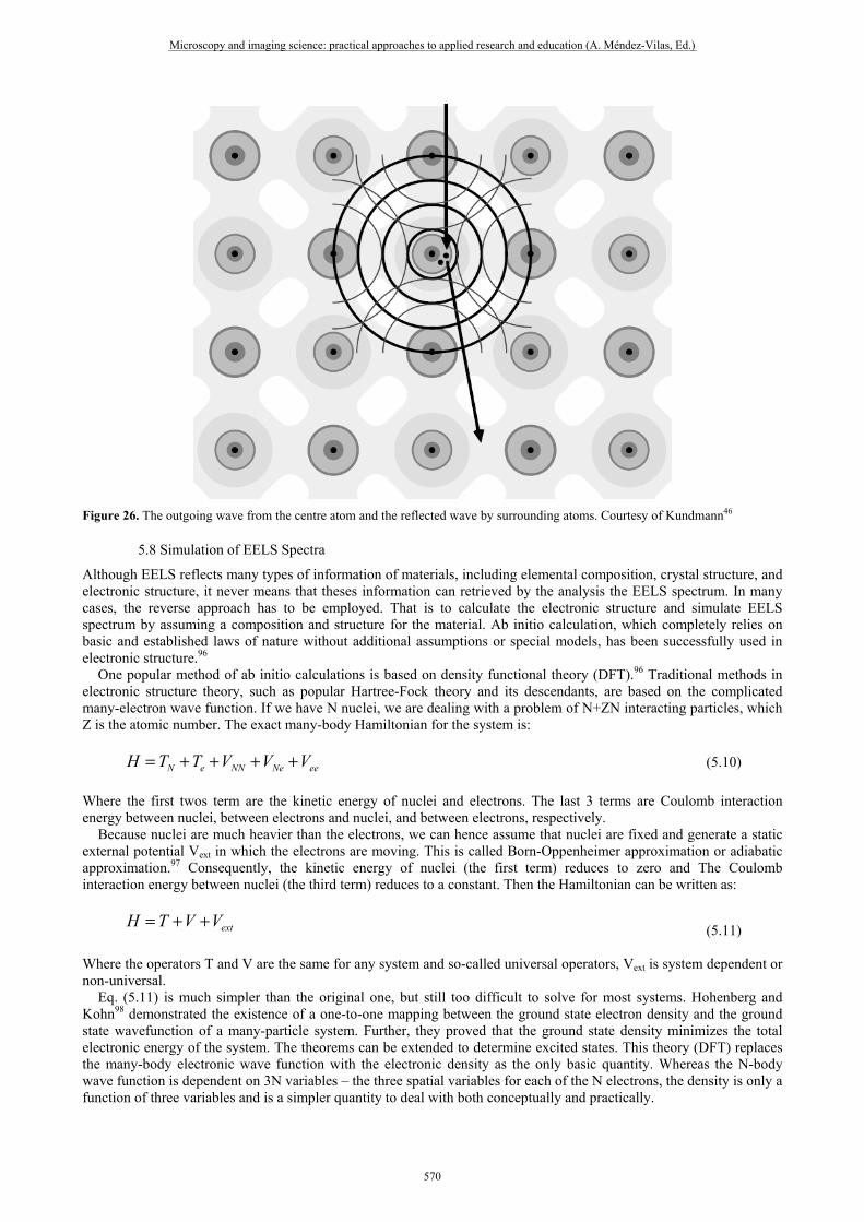
Figure 26. The outgoing wave from the centre atom and the reflected wave by surrounding atoms. Courtesy of Kundmann46
5.8 Simulation of EELS Spectra
Although EELS reflects many types of information of materials, including elemental composition, crystal structure, and electronic structure, it never means that theses information can retrieved by the analysis the EELS spectrum. In many cases, the reverse approach has to be employed. That is to calculate the electronic structure and simulate EELS spectrum by assuming a composition and structure for the material. Ab initio calculation, which completely relies on basic and established laws of nature without additional assumptions or special models, has been successfully used in electronic structure.96 One popular method of ab initio calculations is based on density functional theory (DFT).96 Traditional methods in electronic structure theory, such as popular Hartree-Fock theory and its descendants, are based on the complicated many-electron wave function. If we have N nuclei, we are dealing with a problem of N+ZN interacting particles, which Z is the atomic number. The exact many-body Hamiltonian for the system is:
N e NN Ne eeH T T V V V= + + + + (5.10)
Where the first twos term are the kinetic energy of nuclei and electrons. The last 3 terms are Coulomb interaction energy between nuclei, between electrons and nuclei, and between electrons, respectively. Because nuclei are much heavier than the electrons, we can hence assume that nuclei are fixed and generate a static external potential Vext in which the electrons are moving. This is called Born-Oppenheimer approximation or adiabatic approximation.97 Consequently, the kinetic energy of nuclei (the first term) reduces to zero and The Coulomb interaction energy between nuclei (the third term) reduces to a constant. Then the Hamiltonian can be written as:
extH T V V= + + (5.11)
Where the operators T and V are the same for any system and so-called universal operators, Vext is system dependent or non-universal. Eq. (5.11) is much simpler than the original one, but still too difficult to solve for most systems. Hohenberg and Kohn98 demonstrated the existence of a one-to-one mapping between the ground state electron density and the ground state wavefunction of a many-particle system. Further, they proved that the ground state density minimizes the total electronic energy of the system. The theorems can be extended to determine excited states. This theory (DFT) replaces the many-body electronic wave function with the electronic density as the only basic quantity. Whereas the N-body wave function is dependent on 3N variables – the three spatial variables for each of the N electrons, the density is only a function of three variables and is a simpler quantity to deal with both conceptually and practically.
Microscopy and imaging science: practical approaches to applied research and education (A. Méndez-Vilas, Ed.)
570
___________________________________________________________________________________________
The most common implementation of DFT is through the Kohn-Sham method.99, 100 In the framework of Kohn-Sham, the intractable many-body problem of interacting electrons in a static external potential is reduced to a tractable problem of non-interacting electrons moving in an effective potential. The effective potential includes the external potential Vext and the effects of the Coulomb interactions between the electrons, including the exchange Vx and correlation interactions Vc.
0 ( )KS H x cH T V V V= + + + (5.12)
Where T0 is the functional for the kinetic energy of a non-interacting electron gas, VH stands for the Hartree contribution
of interaction between electrons.101 The single-particle wave functions ( )i rφ cab be obtained by minimizing the
energy of the Kohn-Sham equation:
KS i i iH ψ ε ψ= (5.13)
Then the exact ground-state density ( )rρ of an N-electron system is
( ) ( ) ( )1
*N
i ii
r r rρ ψ ψ=
= (5.14)
Now the task is to solve the Kohn-Sham equation. Because ( )rρ is determined by Kohn-Sham equation, where
both the Hartree operator VH and the exchange-correlation operator Vxc depend on the density ( )rρ . This means we
are dealing with a self-consistency problem. In ab initio calculation, a guessed ( )i rρ is input first. Then the Kohn-
Sham Hamiltonian is constructed from ( )i rρ . After solving Kohn-Sham equation, a new electron density ( )1i rρ +
is
calculated from wave function. If the ( )1i rρ +
is equal to the initially guessed ( )i rρ , then ( )i rρ
is self consistent
and is output. Otherwise the new ( )1i rρ +
is input again for the i+1 cycle. The flow chart of ab initio calculation based
on DFT is shown in Figure 27.
Microscopy and imaging science: practical approaches to applied research and education (A. Méndez-Vilas, Ed.)
571
___________________________________________________________________________________________
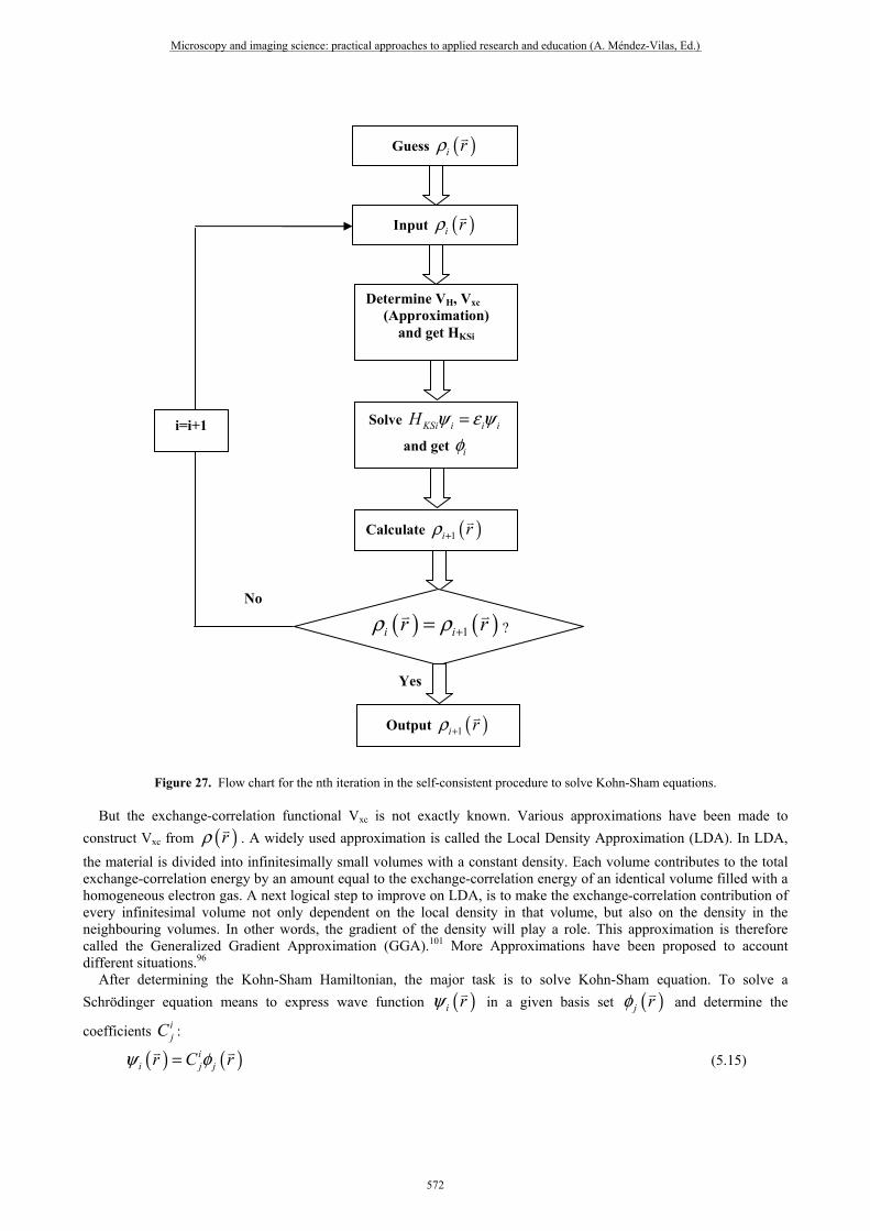
Figure 27. Flow chart for the nth iteration in the self-consistent procedure to solve Kohn-Sham equations. But the exchange-correlation functional Vxc is not exactly known. Various approximations have been made to
construct Vxc from ( )rρ . A widely used approximation is called the Local Density Approximation (LDA). In LDA,
the material is divided into infinitesimally small volumes with a constant density. Each volume contributes to the total exchange-correlation energy by an amount equal to the exchange-correlation energy of an identical volume filled with a homogeneous electron gas. A next logical step to improve on LDA, is to make the exchange-correlation contribution of every infinitesimal volume not only dependent on the local density in that volume, but also on the density in the neighbouring volumes. In other words, the gradient of the density will play a role. This approximation is therefore called the Generalized Gradient Approximation (GGA).101 More Approximations have been proposed to account different situations.96 After determining the Kohn-Sham Hamiltonian, the major task is to solve Kohn-Sham equation. To solve a
Schrödinger equation means to express wave function ( )i rψ in a given basis set ( )j rφ
and determine the
coefficients ijC :
( ) ( )ii j jr C rψ φ=
(5.15)
Input ( )i rρ
Guess ( )i rρ
Determine VH, Vxc (Approximation)
and get HKSi
Solve KSi i i iH ψ ε ψ=
and get iφ
Calculate ( )1i rρ +
( ) ( )1i ir rρ ρ += ?
Output ( )1i rρ +
Yes
No
i=i+1
Microscopy and imaging science: practical approaches to applied research and education (A. Méndez-Vilas, Ed.)
572
___________________________________________________________________________________________

If the functions of the basis set are very similar to ( )i rψ , only a few of them is enough to accurately describe the
wave function. Otherwise the number of basis functions needed is much higher than what is affordable. The art of ab initio calculation is to find a good basis set. As well known, free electrons are described by plane waves (PWs).18 A periodic Hamiltonian can also be expressed exactly in this basis set of plane waves (PWs), known as Bloch waves. However, PW is no longer a good basis set near the nucleus. Space is therefore divided in two regions: A spherical region around each atom a sphere is often called muffin tin region (RMT); the remaining space outside the spheres is called the interstitial region. While in the interstitial region a basis set can be constructed with PWs, in RMT local orbitals are more effective for constructing the basis set. In this way, a basis set is constructed with augmented plane waves (APWs). APW method is of no practical use any more today due to its inefficiency. Its descendants, such as Linearized Augmented Plane Wave (LAPW) and LAPW+lo (local orbitals), are widely used. WIEN2k and its ascendants WIEN97 is a full-potential LAPW-code for crystalline solids.102 WIEN2k includes a program for ELNES simulation. The TELNES.2 program calculates the double differential scattering cross section (DDSCS) on a grid of energy loss values and scattering impulse vectors.103 This double differential cross section is integrated to yield a (single) differential cross section. The carbon K-edges from experiments and calculations by WIEN97 are shown in Figure 28. Another method is based on multiple-scattering theory (MST).104 MST can be used to calculate the electronic structure of an arbitrary assembly of atoms. Its application to periodic solids, known as the Korringa- Kohn-Rostoker (KKR) method, has been widely used to study the electronic structure of solids.105 MST has been used to interpret x-ray absorption near edge structure (XANES),106, 107 and recently been used to EELS.106, 108 This technique is based on the interference between the outgoing electron wave of the excited electron, and the elastically backscattered wave by the surrounding atoms in the solid. Figure 28 shows the carbon K-edges from experiments and calculations by WIEN97 (based on DFT), FEFF8 and ICXANES (both based on MST).109
Figure 28. Comparison of carbon K-edge spectra of TiC: (a) experimental, (b) FLAPW, (c) FEFF8, and (d) ICXANES.109 Copyright American Physical Society. Reproduced with permission.
Microscopy and imaging science: practical approaches to applied research and education (A. Méndez-Vilas, Ed.)
573
___________________________________________________________________________________________

6. EELS Imaging
In addition to the EELS spectrum, electron energy loss also adds a new dimension to the imaging. Many new imaging techniques and applications appear by combining the high spatial resolution imaging and diffraction capabilities of TEM/STEM and the versatile analytical capabilities of EELS. The EELS related imaging can be classified into energy filtered transmission electron microscopy (EFTEM) and spectrum imaging (SI) with STEM.
6.1 Energy Filtered Transmission Electron Microscopy
An energy loss filter with energy selection slit on the TEM allows selecting a very narrow window of energies in the EELS spectrum. The electrons with specific energy loss are then used for imaging the diffraction. This technique is known as energy filtered transmission electron microscopy (EFTEM),110-112 sometimes called electron spectroscopic imaging (ESI);113 EFTEM essentially utilizes the rich information provided by EELS in imaging and diffraction manner.114 Figure 29 illustrates the working principles of EFTEM. EFTEM works much like the conventional TEM except that the electrons with specific energy loss E are used to form images or diffraction. As a result, in addition to the spatial coordinates x and y, the energy loss E stands out as a third dimension.
Figure 29. A schematic diagram showing the working principle of EFTEM. Energy loss E works as an additional dimension to the spatial dimensions (x, y). It is instructive to compare EFTEM and bright-field (BF) / dark-field (DF) imaging.115 In EFTEM, the electrons with specific energy loss are selected with the energy selection slit to form images or diffraction. In BF/DF imaging, the electrons with specific scattering (mostly elastic) angle are selected with objective aperture to form images. As pointed out by Gerald Kothleitner,115 the two techniques have analogies in many aspects, as shown in Table 2.
Microscopy and imaging science: practical approaches to applied research and education (A. Méndez-Vilas, Ed.)
574
___________________________________________________________________________________________
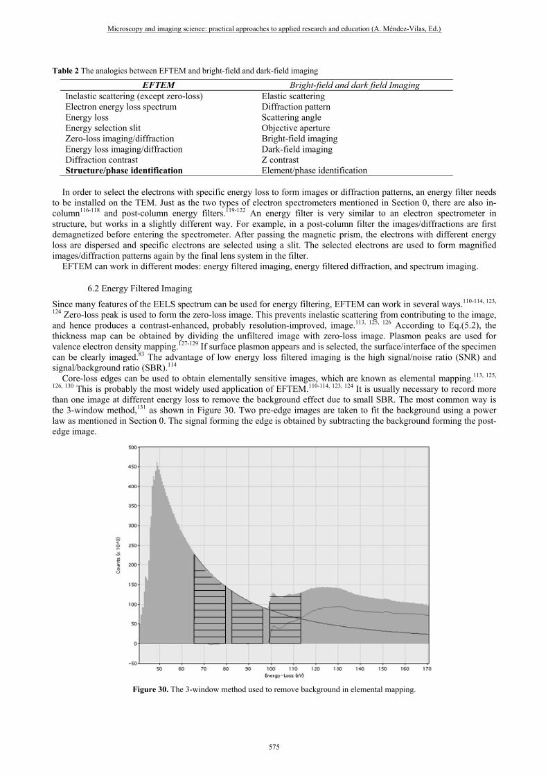
Table 2 The analogies between EFTEM and bright-field and dark-field imaging
EFTEM Bright-field and dark field Imaging Inelastic scattering (except zero-loss) Elastic scattering Electron energy loss spectrum Diffraction pattern Energy loss Scattering angle Energy selection slit Objective aperture Zero-loss imaging/diffraction Bright-field imaging Energy loss imaging/diffraction Dark-field imaging Diffraction contrast Z contrast Structure/phase identification Element/phase identification
In order to select the electrons with specific energy loss to form images or diffraction patterns, an energy filter needs to be installed on the TEM. Just as the two types of electron spectrometers mentioned in Section 0, there are also in-column116-118 and post-column energy filters.119-122 An energy filter is very similar to an electron spectrometer in structure, but works in a slightly different way. For example, in a post-column filter the images/diffractions are first demagnetized before entering the spectrometer. After passing the magnetic prism, the electrons with different energy loss are dispersed and specific electrons are selected using a slit. The selected electrons are used to form magnified images/diffraction patterns again by the final lens system in the filter. EFTEM can work in different modes: energy filtered imaging, energy filtered diffraction, and spectrum imaging.
6.2 Energy Filtered Imaging
Since many features of the EELS spectrum can be used for energy filtering, EFTEM can work in several ways.110-114, 123,
124 Zero-loss peak is used to form the zero-loss image. This prevents inelastic scattering from contributing to the image, and hence produces a contrast-enhanced, probably resolution-improved, image.113, 125, 126 According to Eq.(5.2), the thickness map can be obtained by dividing the unfiltered image with zero-loss image. Plasmon peaks are used for valence electron density mapping.127-129 If surface plasmon appears and is selected, the surface/interface of the specimen can be clearly imaged.83 The advantage of low energy loss filtered imaging is the high signal/noise ratio (SNR) and signal/background ratio (SBR).114 Core-loss edges can be used to obtain elementally sensitive images, which are known as elemental mapping.113, 125,
126, 130 This is probably the most widely used application of EFTEM.110-114, 123, 124 It is usually necessary to record more than one image at different energy loss to remove the background effect due to small SBR. The most common way is the 3-window method,131 as shown in Figure 30. Two pre-edge images are taken to fit the background using a power law as mentioned in Section 0. The signal forming the edge is obtained by subtracting the background forming the post-edge image.
Figure 30. The 3-window method used to remove background in elemental mapping.
Microscopy and imaging science: practical approaches to applied research and education (A. Méndez-Vilas, Ed.)
575
___________________________________________________________________________________________
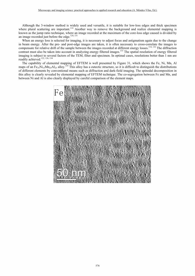
Although the 3-window method is widely used and versatile, it is suitable for low-loss edges and thick specimen where plural scattering are important.114 Another way to remove the background and realize elemental mapping is known as the jump ratio technique, where an image recorded at the maximum of the core-loss edge caused is divided by an image recorded just before the edge.124, 131 When an energy loss is selected for imaging, it is necessary to adjust focus and astigmatism again due to the change in beam energy. After the pre- and post-edge images are taken, it is often necessary to cross-correlate the images to compensate for relative drift of the sample between the images recorded at different energy losses.114, 132 The diffraction contrast must also be taken into account in analyzing energy filtered images.133 The spatial resolution of energy filtered imaging is subject to several factors of the TEM, filter and specimen. In optimal cases, resolutions better than 1 nm are readily achieved.122, 126, 134 The capability of elemental mapping of EFTEM is well presented by Figure 31, which shows the Fe, Ni, Mn, Al maps of an Fe35Ni15Mn25Al25 alloy.135 This alloy has a eutectic structure, so it is difficult to distinguish the distributions of different elements by conventional means such as diffraction and dark-field imaging. The spinodal decomposition in this alloy is clearly revealed by elemental mapping of EFTEM technique. The co-segregation between Fe and Mn, and between Ni and Al is also clearly displayed by careful comparison of the element maps.
50 nm50 nm
Fe
Microscopy and imaging science: practical approaches to applied research and education (A. Méndez-Vilas, Ed.)
576
___________________________________________________________________________________________

50 nm50 nm
N i
50 nm50 nm
M n
Microscopy and imaging science: practical approaches to applied research and education (A. Méndez-Vilas, Ed.)
577
___________________________________________________________________________________________
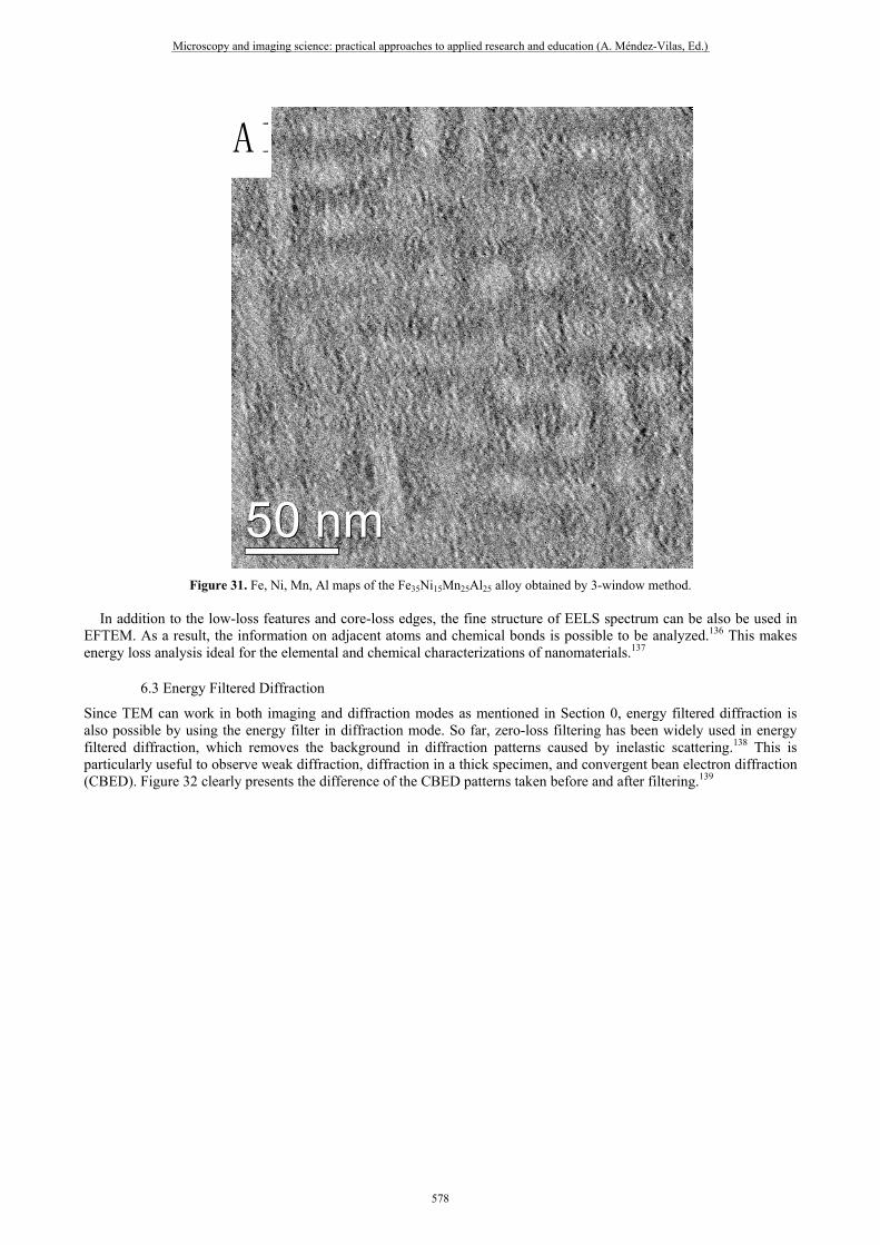
50 nm50 nm
Al
Figure 31. Fe, Ni, Mn, Al maps of the Fe35Ni15Mn25Al25 alloy obtained by 3-window method. In addition to the low-loss features and core-loss edges, the fine structure of EELS spectrum can be also be used in EFTEM. As a result, the information on adjacent atoms and chemical bonds is possible to be analyzed.136 This makes energy loss analysis ideal for the elemental and chemical characterizations of nanomaterials.137
6.3 Energy Filtered Diffraction
Since TEM can work in both imaging and diffraction modes as mentioned in Section 0, energy filtered diffraction is also possible by using the energy filter in diffraction mode. So far, zero-loss filtering has been widely used in energy filtered diffraction, which removes the background in diffraction patterns caused by inelastic scattering.138 This is particularly useful to observe weak diffraction, diffraction in a thick specimen, and convergent bean electron diffraction (CBED). Figure 32 clearly presents the difference of the CBED patterns taken before and after filtering.139
Microscopy and imaging science: practical approaches to applied research and education (A. Méndez-Vilas, Ed.)
578
___________________________________________________________________________________________
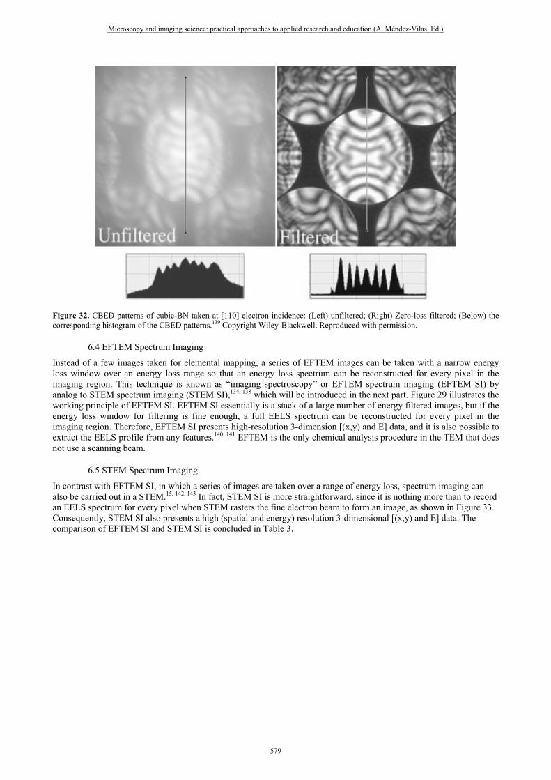
Figure 32. CBED patterns of cubic-BN taken at [110] electron incidence: (Left) unfiltered; (Right) Zero-loss filtered; (Below) the corresponding histogram of the CBED patterns.139 Copyright Wiley-Blackwell. Reproduced with permission.
6.4 EFTEM Spectrum Imaging
Instead of a few images taken for elemental mapping, a series of EFTEM images can be taken with a narrow energy loss window over an energy loss range so that an energy loss spectrum can be reconstructed for every pixel in the imaging region. This technique is known as “imaging spectroscopy” or EFTEM spectrum imaging (EFTEM SI) by analog to STEM spectrum imaging (STEM SI),134, 138 which will be introduced in the next part. Figure 29 illustrates the working principle of EFTEM SI. EFTEM SI essentially is a stack of a large number of energy filtered images, but if the energy loss window for filtering is fine enough, a full EELS spectrum can be reconstructed for every pixel in the imaging region. Therefore, EFTEM SI presents high-resolution 3-dimension [(x,y) and E] data, and it is also possible to extract the EELS profile from any features.140, 141 EFTEM is the only chemical analysis procedure in the TEM that does not use a scanning beam.
6.5 STEM Spectrum Imaging
In contrast with EFTEM SI, in which a series of images are taken over a range of energy loss, spectrum imaging can also be carried out in a STEM.15, 142, 143 In fact, STEM SI is more straightforward, since it is nothing more than to record an EELS spectrum for every pixel when STEM rasters the fine electron beam to form an image, as shown in Figure 33. Consequently, STEM SI also presents a high (spatial and energy) resolution 3-dimensional [(x,y) and E] data. The comparison of EFTEM SI and STEM SI is concluded in Table 3.
Microscopy and imaging science: practical approaches to applied research and education (A. Méndez-Vilas, Ed.)
579
___________________________________________________________________________________________

Figure 33. A schematic diagram showing the working principle of STEM SI. Every pixel at (x,y) contains a full EELS spectrum. Table 3 The comparison of EFTEM SI and STEM SI. After John A. Hunt.144
EFTEM SI STEM SI In a TEM In a STEM An energy filtered image every time An EELS spectrum every time A stack of energy filtered images A stack of EELS spectra High quality spectra Low quality spectra Slow for elemental mapping Fast for elemental mapping High energy resolution - determined by EELS Low energy resolution – determined by energy
selection slit Spatial resolution determined by beam size (better than 1 nm for field emission gun)
Spatial resolution similar to energy filtered imaging (better than 1 nm for field emission gun)
7. Applications to Diluted Magnetic Semiconductors
7.1 Introduction
Doping is a well known and effective method for engineering the electrical, optical, magnetic, and other physical properties of host semiconductors. Incorporation of a few percent of 3d transition-metal ions (e.g., Mn2+, Cr2+, and Co2+) can make non-magnetic semiconductors magnetic. This type of material is called diluted magnetic semiconductors (DMSs). DMSs are of particular interest due to the potential use in next-generation electronics – spintronics, which exploits both spin and charge degree of freedom of electrons.145-148 In fact, many DMSs have been found to be ferromagnetic at and above room temperature. However, it is largely of enormous challenge to fully understand the underlying microscopic origin of the observed magnetism. 149, 150 EELS allows the probe of electronic structures of DMSs and the spatial distributions of transition metals in the host semiconductors.151 Thus, it may give insightful information on the debated problems such as origins of ferromagnetism in DMSs. The high-resolution EELS studies of DMSs are expected to be growing. Here, an example of the EELS applications to the DMSs is demonstrated.152
Microscopy and imaging science: practical approaches to applied research and education (A. Méndez-Vilas, Ed.)
580
___________________________________________________________________________________________

7.2 Experimental
Zn1-xCoxO (0<x<0.1) DMS samples were synthesized by a mild solvothermal technique, whose detailed experimental procedure was described elsewhere.152 The EELS spectra were obtained using a GIF on a FEI Tecnai 20 FEG TEM operated at 200 kV. The energy resolution is about 1.1 eV. The EELS spectra were acquired using a point probe with a spot size of ca. 10 nm, which determines the spatial resolution of the chemical information obtained.
7.3 Results and Discussion
Our analytical TEM studies using EELS reveal that the solvothermal method is indeed highly effective at producing nanocrystalline materials. A typical TEM image of the Zn1-xCoxO (x = 0.098) sample is displayed in Figure 34 (a), in which one can see both nanoparticles and nanorods. The contrast observed at the particle surfaces does not arise from a core-sheath configuration, but instead is due to an abrupt thickness change in the surface regions. The Co-L EELS spectra taken at different locations on a nanorod are illustrated in Figure 35(b), along with the standard CoO spectra from the Gatan database [shown at the bottom of Figure 35 (b)]. The spectra obtained on standard CoO and the standard Co3O4 commercial chemicals are shown in Figure 35(c) for the comparison with that of the Zn1-xCoxO nanocrystals. The Co-L2 and L3 edge corresponds to electron excitation from the 2p1/2 and 2p3/2 level to the empty states in the 3d band. Because the 3d band is very narrow, the L2,3 edges display sharp white lines. It is clearly visible that Co3O4 displays different L2,3 edge ratios from CoO and doped nanocrystals. Thus, the local environment of Co in the ZnO lattice resembles that of CoO. The shape of L2,3 peaks and their area ratios at different locations (after appropriate removal of the background and plural scattering) correlate well with that of standard CoO rather than Co3O4.
152 This further suggests that the valence state of Co be unambiguously divalent in the host ZnO. It can be also concluded that the distribution of the Co dopant in the host lattice is largely homogeneous.
50 nm
(a)
770 780 790 800 810 820
Background-subtracted Plural-scattering-corrected
Nor
mal
ized
inte
nsity
(a.u
.)
Energy loss (eV)
(b) Co-L3
Co-L2 7
6
5
4
3
2
1
Standard CoO
Microscopy and imaging science: practical approaches to applied research and education (A. Méndez-Vilas, Ed.)
581
___________________________________________________________________________________________

760 770 780 790 800 810 820 830 840
Co-L2
Standard Co3O4 Standard CoO (Zn,Co)O
Inte
nsity
(a.u
.)
Energy loss (eV)
Co-L3(c)
Figure 34. (a) The TEM image of the Zn1-xCoxO (x = 0.098).152 (b) Background-subtracted and plural-scattering-corrected Co-L2,3 edges at different locations of a nanorod shown in (a). The spectra have been acquired at positions marked on the nanorod by numbers.152 (c) The comparison of Co-L2,3 edges acquired from the standard Co3O4, the standard CoO, and Co-doped ZnO nanocrystals after the correction of plural scattering. Copyright Wiley-VCH Verlag GmbH & Co. KGaA. Reproduced with permission. EELS spectra may detect any change resulting from the band structure change due to the hybridization effect or defect mediating, but such a change must be too small (in the order of 0.1 eV) to be identified in the current EELS energy resolution. Moreover, it is difficult to see difference in the EELS spectra for samples with different Co dopant concentration. For example, the Co-L edge for x = 0.020 sample cannot be detected, and the fine structure of Co-L edge is vague for x = 0.056 sample, as shown in Figure 35. There is no such fine structure in EELS for Zn due to the close d hell electronic configuration (the 3d state is full of electrons). Also, such a configuration causes the diamagnetism of the host ZnO.
600 800 1000 1200 1400
O-K
Inte
nsity
(a.u
.)
Energy loss (eV)
Co-L2,3 Zn-L2,3
780 840 900 960 1020 1080
Inte
nsity
(a.u
.)
Zn-L2,3
Energy loss (eV)
Co-L2,3
Figure 35 The EELS spectrum of the Zn1-xCoxO (x = 0.056). Inset shows the background subtracted EELS spectrum at Co-L2,3 and Zn-L2,3 edges. However, the white lines of Co-L2,3 edge are too weak to be analysed quantitatively. Figure 36 shows the typical EFTEM elemental mapping of two adjacent nanoparticles for the Zn1-xCoxO (x = 0.056) [see Figure 36 (a)], providing direct evidence of successful impurity doping into the host.153 Elemental mapping indicates a relatively homogeneous distribution of Zn, O and Co in the matrix nanoparticles, except in the thin surface layers. The smaller region of Co mapping in Figure 36 (d) is qualitatively ascribed to the smaller Co concentration in the thin surface layers. Such an inhomogeneity of dopant is a generic phenomenon in DMSs and may compromise the target physical properties of the doped nanocrystals.152, 153 Although chemical inhomogeneity as a whole is observed, the significant changes in the structures from the corresponding fast Fourier transform patterns are not observed. Dopants located in the surface sites may differ quite considerably from those in the cores in their geometries, electronic structures, redox potentials, and physical properties.
Microscopy and imaging science: practical approaches to applied research and education (A. Méndez-Vilas, Ed.)
582
___________________________________________________________________________________________
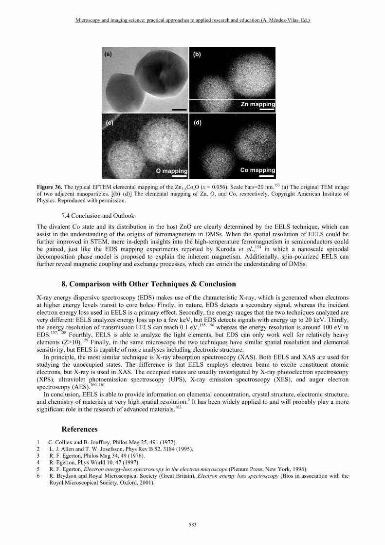
(a)
Zn mapping
(b)
O mapping
(c)
Co mapping
(d)
Figure 36. The typical EFTEM elemental mapping of the Zn1-xCoxO (x = 0.056). Scale bars=20 nm.153 (a) The original TEM image of two adjacent nanoparticles. [(b)–(d)] The elemental mapping of Zn, O, and Co, respectively. Copyright American Institute of Physics. Reproduced with permission.
7.4 Conclusion and Outlook
The divalent Co state and its distribution in the host ZnO are clearly determined by the EELS technique, which can assist in the understanding of the origins of ferromagnetism in DMSs. When the spatial resolution of EELS could be further improved in STEM, more in-depth insights into the high-temperature ferromagnetism in semiconductors could be gained, just like the EDS mapping experiments reported by Kuroda et al.,154 in which a nanoscale spinodal decomposition phase model is proposed to explain the inherent magnetism. Additionally, spin-polarized EELS can further reveal magnetic coupling and exchange processes, which can enrich the understanding of DMSs.
8. Comparison with Other Techniques & Conclusion
X-ray energy dispersive spectroscopy (EDS) makes use of the characteristic X-ray, which is generated when electrons at higher energy levels transit to core holes. Firstly, in nature, EDS detects a secondary signal, whereas the incident electron energy loss used in EELS is a primary effect. Secondly, the energy ranges that the two techniques analyzed are very different: EELS analyzes energy loss up to a few keV, but EDS detects signals with energy up to 20 keV. Thirdly, the energy resolution of transmission EELS can reach 0.1 eV,155, 156 whereas the energy resolution is around 100 eV in EDS.157, 158 Fourthly, EELS is able to analyze the light elements, but EDS can only work well for relatively heavy elements (Z>10).159 Finally, in the same microscope the two techniques have similar spatial resolution and elemental sensitivity, but EELS is capable of more analyses including electronic structure. In principle, the most similar technique is X-ray absorption spectroscopy (XAS). Both EELS and XAS are used for studying the unoccupied states. The difference is that EELS employs electron beam to excite constituent atomic electrons, but X-ray is used in XAS. The occupied states are usually investigated by X-ray photoelectron spectroscopy (XPS), ultraviolet photoemission spectroscopy (UPS), X-ray emission spectroscopy (XES), and auger electron spectroscopy (AES).160, 161 In conclusion, EELS is able to provide information on elemental concentration, crystal structure, electronic structure, and chemistry of materials at very high spatial resolution.5 It has been widely applied to and will probably play a more significant role in the research of advanced materials.162
References 1 C. Colliex and B. Jouffrey, Philos Mag 25, 491 (1972). 2 L. J. Allen and T. W. Josefsson, Phys Rev B 52, 3184 (1995). 3 R. F. Egerton, Philos Mag 34, 49 (1976). 4 R. Egerton, Phys World 10, 47 (1997). 5 R. F. Egerton, Electron energy-loss spectroscopy in the electron microscope (Plenum Press, New York, 1996). 6 R. Brydson and Royal Microscopical Society (Great Britain), Electron energy loss spectroscopy (Bios in association with the
Royal Microscopical Society, Oxford, 2001).
Microscopy and imaging science: practical approaches to applied research and education (A. Méndez-Vilas, Ed.)
583
___________________________________________________________________________________________

7 B. Fultz, in Transmission Electron Energy Loss Spectrometry in Materials Science and The EELS Atlas (Second Edition), edited by C. C. Ahn, 2005), p. 1.
8 J. Hillier and R. F. Baker, J Appl Phys 15, 663 (1944). 9 P. E. Batson, Nature 366, 727 (1993). 10 P. E. Batson, Ultramicroscopy 78, 33 (1999). 11 Z. L. Wang and J. M. Cowley, Surf Sci 193, 501 (1988). 12 H. Ibach, Electron energy loss spectrometers : the technology of high performance (Springer-Verlag, Berlin ; New York, 1991). 13 R. F. Egerton, in Transmission Electron Energy Loss Spectrometry in Materials Science and The EELS Atlas (Second Edition),
edited by C. C. Ahn, 2005), p. 21. 14 N. D. Browning, D. J. Wallis, P. D. Nellist, and S. J. Pennycook, Micron 28, 333 (1997). 15 M. Bosman, Thesis (Ph D ), Electron Microscope Unit, Faculty of Science, University of Sydney, 2007., 2006. 16 O. Oldenberg and W. G. Holladay, Introduction to atomic and nuclear physics (McGraw-Hill, New York,, 1967). 17 C. C. Ahn and O. L. Krivanek, EELS Atlas (Gatan Inc., Warrendale, 1983). 18 C. Kittel, Introduction to solid state physics (Wiley, Hoboken, NJ, 2005). 19 P. Nozieres and D. Pines, Phys Rev 1, 1254 (1959). 20 P. A. Thiry, M. Liehr, J. J. Pireaux, and R. Caudano, Phys Scripta 35, 368 (1987). 21 L. Reimer, Transmission electron microscopy : physics of image formation and microanalysis (Springer-Verlag, Berlin ; New
York, 1989). 22 Z. L. Wang, Elastic and inelastic scattering in electron diffraction and imaging (Plenum Press, New York, 1995). 23 M. De Crescenzi and M. N. Piancastelli, Electron scattering and related spectroscopies (World Scientific, Singapore, 1996). 24 B. Fultz and J. M. Howe, Transmission electron microscopy and diffractometry of materials (Springer, Berlin ; New York,
2002). 25 I. D. Williams, B. Srigengan, J. B. Greenwood, W. R. Newell, A. Platzer, and L. OHagan, Phys Scripta T73, 119 (1997). 26 P. Dumas and Y. J. Chabal, Chem Phys Lett 181, 537 (1991). 27 A. Rizzi, H. Moritz, and H. Luth, J Vac Sci Technol A 9, 912 (1991). 28 V. N. Baier and V. M. Katkov, Phys Rev D 5905 (1999). 29 J. C. Fuggle and J. E. Inglesfield, Top Appl Phys 69, 1 (1992). 30 R. E. Camley and D. L. Mills, Phys Rev B 29, 1695 (1984). 31 R. Matz and H. Luth, Phys Rev Lett 46, 500 (1981). 32 P. M. T. M. Vanattekum and J. M. Trooster, Phys Rev B 20, 2335 (1979). 33 Z. J. Ding, H. M. Li, Q. R. Pu, Z. M. Zhang, and R. Shimizu, Phys Rev B 66 (2002). 34 A. Yelon, K. N. Piyakis, and E. Sacher, Surf Sci 569, 47 (2004). 35 F. J. Pijper and P. Kruit, Phys Rev B 44, 9192 (1991). 36 A. J. Bourdillon and C. L. Cha, Phil Mag Lett 74, 113 (1996). 37 P. Schattschneider and P. Pongratz, Scanning Microscopy, 27 (1990). 38 M. Knupfer, E. Zojer, G. Leising, and J. Fink, Synthetic Met 119, 499 (2001). 39 K. Leifer, S. Mautino, H. Weman, A. Rudra, E. Pelucchi, F. Bobard, A. Wyser, and E. Kapon, Inst Phys Conf Ser, 131 (2003). 40 M. Ghamnia, C. Jardin, L. Martinez, M. Bouslama, and P. Durupt, Vacuum 48, 129 (1997). 41 J. L. Robins and J. B. Swan, P Phys Soc Lond 76, 857 (1960). 42 J. L. Robins, P Phys Soc Lond 78, 1177 (1961). 43 P. Stadelmann, K. Leifer, and C. Verdon, Ultramicroscopy 58, 35 (1995). 44 M. Watanabe, D. B. Williams, and Y. Tomokiyo, Micron 34, 173 (2003). 45 G. Gergely, Surf Interface Anal 3, 201 (1981). 46 M. Kundmann, in Gatan EELS School, Pleasanton, California, USA, 2004). 47 D. S. Su, H. F. Wang, and E. Zeitler, Ultramicroscopy 59, 181 (1995). 48 R. F. Egerton and Z. L. Wang, Ultramicroscopy 32, 137 (1990). 49 H. O. Moltaji, J. P. Buban, and N. D. Browning, J Synchrotron Radiat 6, 326 (1999). 50 B. G. Frederick, B. B. Frederick, and N. V. Richardson, Surf Sci 368, 82 (1996). 51 P. A. M. Dirac, Proceedings of the Royal Society of London Series a-Containing Papers of a Mathematical and Physical
Character 114, 243 (1927). 52 H. A. Bethe, Intermediate quantum mechanics (W.A. Benjamin, New York, 1968). 53 M. Inokuti, Y. Itikawa, and J. E. Turner, Rev Mod Phys 50, 23 (1978). 54 M. Inokuti, Rev Mod Phys 43, 297 (1971). 55 R. Leapman, in Transmission Electron Energy Loss Spectrometry in Materials Science and The EELS Atlas (Second Edition),
edited by C. C. Ahn, 2005), p. 49. 56 D. B. Williams and C. B. Carter, Transmission electron microscopy : a textbook for materials science (Plenum Press, New
York, 1996). 57 B. G. Williams, Prog Solid State Ch 17, 87 (1987). 58 N. D. Browning, M. F. Chisholm, and S. J. Pennycook, Nature 366, 143 (1993). 59 A. V. Crewe, M. Isaacson, and D. Johnson, Rev Sci Instrum 40, 241 (1969). 60 C. Mitterbauer, G. Kothleitner, W. Grogger, H. Zandbergen, B. Freitag, P. Tiemeijer, and F. Hofer, Ultramicroscopy 96, 469
(2003). 61 H. Johnston, in Phys World (Institute of Physics, 2007). 62 A. Gloter, A. Douiri, M. Tence, and C. Colliex, Ultramicroscopy 96, 385 (2003). 63 T. Walther and H. Stegmann, Microsc Microanal 12, 498 (2006). 64 Y. Y. Yang and R. F. Egerton, Microsc Res Techniq 21, 361 (1992). 65 V. J. Keast, A. J. Scott, R. Brydson, D. B. Williams, and J. Bruley, J Microsc-Oxford 203, 135 (2001).
Microscopy and imaging science: practical approaches to applied research and education (A. Méndez-Vilas, Ed.)
584
___________________________________________________________________________________________

66 S. Schamm and G. Zanchi, Ultramicroscopy 88, 211 (2001). 67 J. L. Feng, R. Ho, Z. Shao, and A. P. Somlyo, Ultramicroscopy 76, 221 (1999). 68 Gatan_Inc., DigitalMicrograph EELS Analysis User's Guide, Pleasanton, CA 94588, USA, 2003). 69 U. Bangert, A. J. Harvey, and R. Keyse, Ultramicroscopy 68, 173 (1997). 70 P. Rez, in Transmission Electron Energy Loss Spectrometry in Materials Science and The EELS Atlas (Second Edition), edited
by C. C. Ahn, 2005), p. 97. 71 R. Brydson, Mater Sci Tech Ser 16, 1187 (2000). 72 M. Unser, J. R. Ellis, T. Pun, and M. Eden, J Microsc-Oxford 145, 245 (1987). 73 M. P. Seah, I. S. Gilmore, and S. J. Spencer, Surf Sci 461, 1 (2000). 74 G. Brockt and H. Lakner, Micron 31, 435 (2000). 75 M. R. Mccartney and M. Gajdardziskajosifovska, Ultramicroscopy 53, 283 (1994). 76 R. F. Egerton and S. C. Cheng, Ultramicroscopy 21, 231 (1987). 77 T. Malis, S. C. Cheng, and R. F. Egerton, J Electron Micr Tech 8, 193 (1988). 78 A. LiBassi, A. C. Ferrari, V. Stolojan, B. K. Tanner, J. Robertson, and L. M. Brown, Diam Relat Mater 9, 771 (2000). 79 M. H. Gass, A. J. Papworth, T. B. Joyce, T. J. Bullough, and P. R. Chalker, Appl Phys Lett 84, 1453 (2004). 80 D. B. Williams and J. W. Edington, 108, 113 (1976). 81 X. J. Zhang, G. Xue, A. Agarwal, R. Tsu, M. A. Hasan, J. E. Greene, and A. Rockett, J Vac Sci Technol A 11, 2553 (1993). 82 L. A. Bursill, P. A. Stadelmann, J. L. Peng, and S. Prawer, Phys Rev B 49, 2882 (1994). 83 M. Mitome, Y. Bando, D. Golberg, K. Kurashima, Y. Okura, T. Kaneyama, M. Naruse, and Y. Honda, Microsc Res Techniq
63, 140 (2004). 84 J. Nelayah, et al., Nat Phys 3, 348 (2007). 85 V. J. Keast, J Electron Spectrosc 143, 97 (2005). 86 S. Loughin, R. H. French, L. K. DeNoyer, W. Y. Ching, and Y. N. Xu, J Phys D Appl Phys 29, 1740 (1996). 87 L. W. W. E. M. J. M. N. M. J. L. M. H. F. D. Auret, physica status solidi (c) 1, 674 (2004). 88 R. Brydson, H. Sauer, and W. Engel, in Transmission electron energy loss spectrometry in materials science, edited by M. M.
Disko, C. C. Ahn and B. Fultz (TMS, Warrendale, 1992), p. 131. 89 G. J. Auchterlonie, D. R. Mckenzie, and D. J. H. Cockayne, Ultramicroscopy 31, 217 (1989). 90 L. A. J. Garvie, A. J. Craven, and R. Brydson, Am Mineral 79, 411 (1994). 91 F. Hofer and P. Golob, Ultramicroscopy 21, 379 (1987). 92 R. Brydson, H. Sauer, W. Engel, and E. Zeitler, Microsc Microanal M 2, 159 (1991). 93 http://eels.kuicr.kyoto-u.ac.jp/images/carbon.gif 94 T. Sikora, G. Hug, M. Jaouen, and J. J. Rehr, Phys Rev B 62, 1723 (2000). 95 M. Sarikaya, M. Qian, and E. A. Stern, Micron 27, 449 (1996). 96 R. M. Martin, Electronic structure : basic theory and practical methods (Cambridge University Press, Cambridge, UK ; New
York, 2004). 97 M. Born and R. Oppenheimer, Ann Phys-Leipzig 84, 0457 (1927). 98 P. Hohenberg and W. Kohn, Phys Rev B 136, B864 (1964). 99 W. Kohn and L. J. Sham, Phys Rev 140, A1133 (1965). 100 P. Hohenberg and W. Kohn, Phys Rev 136, B864 (1964). 101 S. Cottenier, (Instituut voor Kern- en Stralingsfysica, K.U.Leuven, Belgium, 2002). 102 P. Blaha, K. Schwarz, G. K. H. Madsen, D. Kvasnicka, and J. Luitz, (Institut fur Physikalische und Theoretische Chemie,
Getreidemarkt 9/156, Wien, Austria, 2007). 103 K. Jorissen, J. Luitz, and C. Hebert, A program for the calculation of energyloss near edge structure: the new and improved
telnes.2 code (2005). 104 P. Sheng, Scattering and localization of classical waves in random media (World Scientific, Singapore ; Teaneck, NJ, 1990). 105 X. G. Zhang and W. H. Butler, Phys Rev B 46, 7433 (1992). 106 Z. Y. Wu, G. Ouvrard, P. Gressier, and C. R. Natoli, Phys Rev B 55, 10382 (1997). 107 P. Rez, J. M. MacLaren, and D. K. Saldin, Phys Rev B 57, 2621 (1998). 108 M. Wibbelt, H. Kohl, and P. Kohler-Redlich, Phys Rev B 59, 11739 (1999). 109 A. J. Scott, R. Brydson, M. MacKenzie, and A. J. Craven, Phys Rev B 63, 245105 (2001). 110 L. Reimer, Adv Electron El Phys 81, 43 (1991). 111 L. Reimer, I. Fromm, P. Hirsch, U. Plate, and R. Rennekamp, Ultramicroscopy 46, 335 (1992). 112 L. Reimer, I. Fromm, and R. Rennekamp, Ultramicroscopy 24, 339 (1988). 113 F. Hofer, P. Warbichler, and W. Grogger, Ultramicroscopy 59, 15 (1995). 114 F. Hofer and W. Peter, in Transmission Electron Energy Loss Spectrometry in Materials Science and The EELS Atlas (Second
Edition), edited by C. C. Ahn, 2005), p. 159. 115 G. Kothleitner, in EELS Imaging and Analysis Training School, Pleasanton, California, USA, 2004). 116 K. Tsuno, T. Kaneyama, T. Honda, K. Tsuda, M. Terauchi, and M. Tanaka, J Electron Microsc 46, 357 (1997). 117 W. Probst, G. Benner, J. Bihr, and E. Weimer, Adv Mater 5, 297 (1993). 118 Y. Tanishiro, K. Okamoto, M. Takeguchi, H. Minoda, T. Suzuki, and K. Yagi, J Electron Microsc 48, 837 (1999). 119 R. Grimm, D. Typke, and W. Baumeister, J Microsc-Oxford 190, 339 (1998). 120 D. Heinemann and W. Mader, Ultramicroscopy 74, 113 (1998). 121 C. Quintana, S. Marco, and J. L. Carrascosa, J Trace Microprobe T 15, 175 (1997). 122 O. L. Krivanek, A. J. Gubbens, N. Dellby, and C. E. Meyer, Microsc Microanal M 3, 187 (1992). 123 F. Hofer, W. Grogger, G. Kothleitner, and P. Warbichler, Ultramicroscopy 67, 83 (1997). 124 F. Hofer, W. Grogger, P. Warbichler, and I. Papst, Mikrochim Acta 132, 273 (2000). 125 L. Reimer, I. Fromm, C. Hulk, and R. Rennekamp, Microsc Microanal M 3, 141 (1992).
Microscopy and imaging science: practical approaches to applied research and education (A. Méndez-Vilas, Ed.)
585
___________________________________________________________________________________________
126 A. J. Gubbens and O. L. Krivanek, Ultramicroscopy 51, 146 (1993). 127 U. Golla and A. Putnis, Phys Chem Miner 28, 119 (2001). 128 H. R. Daniels, R. Brydson, A. Brown, and B. Rand, Ultramicroscopy 96, 547 (2003). 129 Z. L. Wang, Micron 27, 265 (1996). 130 C. Jeanguillaume, P. Trebbia, and C. Colliex, Ultramicroscopy 3, 237 (1978). 131 F. Hofer, P. Warbichler, W. Grogger, and O. Lang, Micron 26, 377 (1995). 132 B. Schaffer, W. Grogger, and G. Kothleitner, Ultramicroscopy 102, 27 (2004). 133 K. T. Moore, J. M. Howe, and D. C. Elbert, Ultramicroscopy 80, 203 (1999). 134 J. L. Lavergne, J. M. Martin, and M. Belin, Microsc Microanal M 3, 517 (1992). 135 D. S. R. K. Zheng, Satoko Kuwano, James A. Hanna, Markus K. Wittmann, John Loudis, Ian Baker, Zongwen Liu, Ross
Marceau, Simon P. Ringer, (2005). 136 D. A. Muller, Y. Tzou, R. Raj, and J. Silcox, Nature 366, 725 (1993). 137 J. Mayer and J. M. Plitzko, J Microsc-Oxford 183, 2 (1996). 138 L. Reimer, in Transmission Electron Energy Loss Spectrometry in Materials Science and The EELS Atlas (Second Edition),
edited by C. C. Ahn, 2005), p. 127. 139 M. Tanada, K. Tsuda, M. Terauchi, K. Tsuno, T. Kaneyama, T. Honda, and M. Ishida, J Microsc-Oxford 194, 219 (1999). 140 J. Mayer, U. Eigenthaler, J. M. Plitzko, and F. Dettenwanger, Micron 28, 361 (1997). 141 K. Kimoto, S. Isakozawa, T. Aoyama, and Y. Matsui, J Electron Microsc 50, 523 (2001). 142 J. A. Hunt and D. B. Williams, Ultramicroscopy 38, 47 (1991). 143 C. Colliex, M. Tence, E. Lefevre, C. Mory, H. Gu, D. Bouchet, and C. Jeanguillaume, Mikrochim Acta 114, 71 (1994). 144 J. A. Hunt, in Gatan EELS School, Pleasanton, California, USA, 2004). 145 S. A. Wolf, D. D. Awschalom, R. A. Buhrman, J. M. Daughton, S. von Molnar, M. L. Roukes, A. Y. Chtchelkanova, and D. M.
Treger, Science 294, 1488 (2001). 146 I. Zutic, J. Fabian, and S. Das Sarma, Rev Mod Phys 76, 323 (2004). 147 H. Ohno, Science 281, 951 (1998). 148 J. K. Furdyna, J Appl Phys 64, R29 (1988). 149 S. A. Chambers, T. C. Droubay, C. M. Wang, K. M. Rosso, S. M. Heald, D. A. SchwartZ, K. R. Kittilstved, and D. R. Gamelin,
Mater Today 9, 28 (2006). 150 S. A. Chambers, Surf Sci Rep 61, 345 (2006). 151 S. Ramachandran, A. Tiwari, and J. Narayan, Appl Phys Lett 84, 5255 (2004). 152 X. F. Wang, J. B. Xu, B. Zhang, H. G. Yu, J. Wang, X. X. Zhang, J. G. Yu, and Q. Li, Adv Mater 18, 2476 (2006). 153 X. F. Wang, J. B. Xu, N. Ke, J. G. Yu, J. Wang, Q. Li, H. C. Ong, and R. Zhang, Appl Phys Lett 88 (2006). 154 S. Kuroda, N. Nishizawa, K. Takita, M. Mitome, Y. Bando, K. Osuch, and T. Dietl, Nat Mater 6, 440 (2007). 155 S. Lazar, G. A. Botton, M. Y. Wu, F. D. Tichelaar, and H. W. Zandbergen, Ultramicroscopy 96, 535 (2003). 156 M. Terauchi, R. Kuzuo, F. Satoh, M. Tanaka, K. Tsuno, and J. Ohyama, Microsc Microanal M 2, 351 (1991). 157 D. E. Newbury, Microsc Microanal 12, 527 (2006). 158 A. Niculae, et al., Microsc Microanal 13, 1430 (2007). 159 R. D. Leapman and J. A. Hunt, Microsc Microanal M 2, 231 (1991). 160 J. C. Vickerman, Surface analysis : the principal techniques (John Wiley, Chichester [England] ; New York, 1997). 161 D. J. O'Connor, B. A. Sexton, and R. S. C. Smart, Surface analysis methods in materials science (Springer-Verlag, Berlin ; New
York, 1992). 162 C. C. Ahn, Transmission electron energy loss spectrometry in materials science and the EELS atlas (Wiley, Weinheim ;
[Chichester], 2004).
Microscopy and imaging science: practical approaches to applied research and education (A. Méndez-Vilas, Ed.)
586
___________________________________________________________________________________________