Embed Size (px)
Citation preview


Electromagnetic Compatibility for Device Designand System Integration

Karl-Heinz Gonschorek · Ralf Vick
ElectromagneticCompatibility for DeviceDesign and SystemIntegration
123

ISBN 978-3-642-03289-9 e-ISBN 978-3-642-03290-5DOI 10.1007/978-3-642-03290-5Springer Heidelberg Dordrecht London New York
Library of Congress Control Number: 2009934598
c© Springer-Verlag Berlin Heidelberg 2009This work is subject to copyright. All rights are reserved, whether the whole or part of the material isconcerned, specifically the rights of translation, reprinting, reuse of illustrations, recitation, broadcasting,reproduction on microfilm or in any other way, and storage in data banks. Duplication of this publicationor parts thereof is permitted only under the provisions of the German Copyright Law of September 9,1965, in its current version, and permission for use must always be obtained from Springer. Violationsare liable to prosecution under the German Copyright Law.The use of general descriptive names, registered names, trademarks, etc. in this publication does notimply, even in the absence of a specific statement, that such names are exempt from the relevant protectivelaws and regulations and therefore free for general use.
Cover design: eStudio Calamar S.L.
Printed on acid-free paper
Springer is part of Springer Science+Business Media (www.springer.com)
Prof. Dr.-Ing. Karl-Heinz GonschorekEMV-Beratung - EMC-ConsultantGostritzer Straße 10601217 [email protected]
Prof. Dr.-Ing. Ralf VickLehrstuhl fur ElektromagnetischeVertraglichkeitOtto-von-Guericke-UniversitatMagdeburgInstitut fur Grundlagen derElektrotechnik undElektromagnetische VertraglichkeitPostfach 412039016 [email protected]

Contents
1 Motivation and Overview ................................................................1 1.1 Availability of programs, mentioned in the book....................6 1.2 Availability of the figures, given in the book..........................6
2 Thinking in Voltages, Currents, Fields and Impedances ..............7
3 Electric Fields..................................................................................19 3.1 Effects of electric fields and their calculation .......................22
4 Magnetic Fields ...............................................................................29 4.1 Effects of magnetic fields......................................................29 4.2 Calculation of magnetic field strength of single and
multicore cables ....................................................................31 4.3 Magnetic fields of Geofol transformers ................................34 4.4 Magnetic stray fields of arbitrary arrangements of thin
wires ......................................................................................35 4.4.1 Magnetic field of a four conductor arrangement..........35 4.4.2 Magnetic fields of twisted cables.................................37 4.4.3 Example calculation with the program STRAYF ........39 4.4.4 Peculiarities of magnetic fields of twisted cables ........41
5 Electromagnetic Fields ...................................................................45 5.1 Characterization of Electromagnetic Waves .........................45 5.2 Effects of electromagnetic fields...........................................50 5.3 The elementary dipoles .........................................................54
5.3.1 Distance conversion .....................................................61 5.3.2 Field impedances .........................................................65
5.4 Effective height, effective antenna area, radiation resistance ...............................................................................68
5.5 Estimating the field strength of aperture antennas ................75 5.5.1 Power density and electric field strength in the far
field region ...................................................................76

5.5.2 Power density and electric field strength in the near field region ........................................................... 77
5.5.3 Description of the program APERTUR ....................... 79 5.5.4 Program SAFEDIST .................................................... 79
6 The Interference Model ................................................................. 83 6.1 Galvanic coupling ................................................................. 90
6.1.1 Measures against a galvanic coupling interference...... 92 6.2 Capacitive coupling............................................................... 93
6.2.1 Measures to lower the capacitive coupling .................. 95 6.3 Inductive coupling................................................................. 97
6.3.1 Magnetic decoupling.................................................. 100 6.3.2 Definition of an effective mutual inductance for a
multicore cable........................................................... 101 6.3.3 Measures to reduce the inductive coupling................ 104
6.4 Electromagnetic coupling.................................................... 106 6.4.1 Measures to reduce the electromagnetic coupling ..... 107 6.4.2 The λ/2-coupling model ............................................. 108 6.4.3 Some remarks regarding the estimation of the
electromagnetic coupling ........................................... 111
7 Intrasystem Measures .................................................................. 121 7.1 Some remarks regarding grounding, shielding, cabling,
and filtering ......................................................................... 123 7.1.1 Grounding .................................................................. 123 7.1.2 Shielding .................................................................... 124 7.1.3 Cabling....................................................................... 126 7.1.4 Filtering...................................................................... 129
7.2 Shielding against electric fields - shield of bars.................. 138 7.3 Shielding against magnetic fields........................................ 141
7.3.1 Shielding against static magnetic and very low frequency magnetic fields .......................................... 141
7.3.2 Shielding against medium frequency magnetic fields........................................................................... 149
7.3.3 Two parallel plates shielding against alternating magnetic fields ........................................................... 149
7.3.4 Hollow sphere shielding against magnetic fields....... 150 7.3.5 Hollow cylinder within a lateral magnetic field......... 151 7.3.6 Hollow cylinder within a longitudinal magnetic
field ............................................................................ 151 7.4 Shielding theory according to Schelkunoff – short and
concise................................................................................. 153
VI Contents

Contents VII
7.4.1 Source code of the program SHIELD ........................157 7.5 Leakages, openings, cavity resonances ...............................157
7.5.1 Leakages, signal penetrations ....................................159 7.5.2 Low frequency resonances, cavity resonances...........167
7.6 Cable coupling and cable transfer impedance.....................171 7.6.1 Cable coupling ...........................................................171 7.6.2 Coupling into untwisted and twisted two
conductor cables.........................................................173 7.6.3 Coupling into and between shielded cables ...............175 7.6.4 Cable shield connection at the device input...............200
8 Atmospheric Noise, Electromagnetic Environment and Limit Values ..................................................................................205 8.1 Atmospheric noise sources, electromagnetic
environment.........................................................................206 8.2 Conversion of limit values ..................................................218
8.2.1 Distance conversion ...................................................218 8.2.2 Conversion E H and H E ..................................220
9 EMC Engineering and Analysis ..................................................225 9.1 Development phases of a complex system..........................227
9.1.1 Conceptual phase .......................................................227 9.1.2 Definition phase .........................................................228 9.1.3 Construction and building phase................................230
9.2 EMC- Test planning ............................................................232 9.3 Execution of analysis ..........................................................242
10 Numerical Techniques for Field Calculation .............................247 10.1 Selecting the appropriate technique ....................................249 10.2 Plausibility check ................................................................256 10.3 Application examples of analysis........................................265
10.3.1 Investigation of resonances on a passenger car..........266 10.3.2 Influence of a dielectric material on the radiation
of a printed circuit board............................................267 10.3.3 Radiation of a mobile phone ......................................268 10.3.4 Electromagnetic field on a frigate ..............................269
10.4 Guidelines for using numerical methods.............................271 10.5 Application: Antenna coupling ...........................................275
10.5.1 General remarks to the N-port theory ........................275 10.5.2 Two port parameter....................................................276 10.5.3 Calculation of antenna coupling ................................278 10.5.4 Source code of the program MATCH........................283

VIII Contents
11 Model for Immunity Testing ....................................................... 285 11.1 Standardised immunity test methods................................... 286 11.2 Statistical approach to model the immunity ........................ 288
11.2.1 Malfunction probability ............................................. 289 11.3 Fault frequency function ..................................................... 292
11.3.1 Interpretation of the results of immunity tests ........... 295 11.4 Time variant immunity........................................................ 296
11.4.1 Modelling................................................................... 297 11.4.2 Immunity of microcontroller based equipment.......... 303
A1 Electric Fields of Rod Arrangements.......................................... 307 A1.1 Potential coefficients and partial capacitances.................... 308 A1.2 Horizontal conductors above ground .................................. 309
A1.2.1 Source code of the program HCOND........................ 315 A1.3 Vertical conductors above ground....................................... 315
A1.3.1 Source code of the program VROD........................... 320
A2 Magnetic Stray Fields................................................................... 321 A2.1 Stray field low installation of cables ................................... 321
A2.1.1 The single core cable (case (a) of chapter 4.2)........... 321 A2.1.2 Cable with one forward and one return conductor
(case (b) of chapter 4.2) ............................................. 322 A2.1.3 Use of two forward- and two return conductors
(case (c1) of chapter 4.2) ........................................... 323 A2.1.4 Installation of the forward and return conductors
above a common ground plane (case (c2) of chapter 4.2) ................................................................ 324
A2.1.5 Use of four forward and four return conductors (case (d) of chapter 4.2) ............................................. 325
A2.2 Computer program for predicting magnetic stray fields ..... 327 A2.2.1 Field of a finitely long wire ....................................... 327 A2.2.2 Field of a single layered coil ...................................... 329 A2.2.3 Considering phase relations ....................................... 333 A2.2.4 Source code of the program STRAYF....................... 335
A3 Self and Mutual Inductances ....................................................... 337 A3.1 Mutual inductance between a finitely long conductor on
the y-axis and a trapezoidal area in the xy-plane ................ 337 A3.2 Decomposition of an area in the xy-plane bounded by
straight lines ........................................................................ 340 A3.3 Treatment of arbitrary conductor loops in space................. 341
Contents IX
A3.4 Mutual inductance between 2 circular loops with lateral displacement........................................................................343
A3.5 Source code of the program MUTUAL ..............................345
A4 Elementary Dipoles ......................................................................347 A4.1 Hertzian dipole ....................................................................347
A4.1.1 Prediction of the field strength components for the general case ..........................................................347
A4.1.2 Solution for time harmonic excitation .......................349 A4.2 Current loop (loop antenna) ................................................353 A4.3 Comparison of the wave impedances..................................360
A5 The Polarization Ellipsis ..............................................................361 A5.1 Two dimensional case (Ez=0)..............................................362 A5.2 Three dimensional case – solution in the time domain .......364
A5.2.1 Some consideration regarding the plane of the polarization ellipse .....................................................367
A5.3 Three dimensional case – solution in the frequency range....................................................................................375
A6 Skin Effect and Shielding Theory of Schelkunoff......................377 A6.1 Skin effect of a conducting half space.................................377
A6.1.1 Strong skin effect within a cylindrical conductor ......379 A6.1.2 Weak skin effect within a cylindrical conductor........380
A6.2 Shielding theory according to Schelkunoff .........................380 A6.2.1 Introduction................................................................380 A6.2.2 Necessary equations...................................................381 A6.2.3 Shielding mechanism .................................................382 A6.2.4 Shielding efficiency ...................................................384 A6.2.5 Simple application of Schelkunoff’s theory...............384 A6.2.6 Procedure for a graphical determination of the
shielding efficiency ....................................................386 A6.2.7 Error estimations........................................................390 A6.2.8 Summary ....................................................................392
A7 Example of an EMC-Design Guide for Systems ........................393 A7.1 Grounding ...........................................................................393 A7.2 System filtering ...................................................................395 A7.3 Shielding .............................................................................395 A7.4 Cabling ................................................................................396

A8 25 EMC-Rules for the PCB-Layout and the Device Construction.................................................................................. 401
A9 Easy-to-use Procedure for Predicting the Cable Transfer Impedance ..................................................................................... 409 A9.1 Predicting the voltage ratio with help of an oscilloscope.... 413 A9.2 Predicting the voltage ratio by a network analyzer ............. 415
A10 Capacitances and Inductances of Common Interest ................. 421
A11 Reports of Electromagnetic Incompatibilities............................ 429
A12 Solutions to the Exercises............................................................. 435
A13 Physical Constants and Conversion Relations........................... 455 A13.1 Physical Units and Constants .............................................. 455 A13.2 Conversion table for pressure.............................................. 456 A13.3 Conversion table for energy ................................................ 457 A13.4 Conversion relations for electric and magnetic
quantities ............................................................................. 457 A13.5 Conversion of logarithmic quantities .................................. 458 A13.6 Abbreviations ...................................................................... 459
A14 Bibliography.................................................................................. 461
Index .............................................................................................. 467
X Contents
1 Motivation and Overview
After working for more than 30 years in the field of EMC; having pub-lished numerous papers on the subject of interference, counter measures and numerical field calculation; the idea emerged to collate all experi-ences, successful analysis techniques and solutions into one comprehen-sive book. This was done in 2003/04 and the book was published in 2005 in the German language. Discussions with colleagues and with the pub-lisher revealed that an English version of the book is desirable. Moreover, the discussions suggested, as expected, some areas for improvement. The two main areas of criticism were firstly, the inclusion of extensive program lists and secondly, the chapter regarding filtering.
Regarding the program lists, it was the original wish of the authors to have them printed. These have now been removed but remain available on the web-pages of the authors and in there place more application examples of the programs have been included. Only very small program lists have been left in.
It has been recognized that the chapter concerning filtering is more a concise theoretical treatment of Butterworth filters than a chapter describ-ing the necessary EMC-features. Therefore, this chapter has been ex-tended, showing more elements from the EMC-point of view and giving suggestions for an EMC-justified installation.
Considering the aforementioned arguments, this English version of the German EMC-book ‘EMV für Geräteentwickler und Systemintegratoren’ is not a simple translation, hopefully it is a further development. Neverthe-less more than 90% consists of translated German text.
Which young scientist has not experienced, that he published a paper or gave a presentation at a symposium, all the time being proud of his work. Then afterwards, seeking praise or criticism, learns that feedback is the ex-ception rather than the rule? But nevertheless, the next paper, the next in-vestigation or the next presentation is still prepared with great care and en-thusiasm.
So the idea to write this book rose from the idea to summarize the re-sults of the different publications and presentations; to compile and to show, as far as possible, the inner relations and dependences of the experi-
K.-H. Gonschorek, R. Vick, Electromagnetic Compatibility for Device Design and System Integration, DOI 10.1007/978-3-642-03290-5_1, © Springer-Verlag Berlin Heidelberg 2009

2 1 Motivation and Overview
ences gained in EMC-analysis, EMC-system planning, and defining coun-termeasures to overcome interference.
Shortly after starting it became clear that the degree of experience of a single human being is always limited. Therefore, in order to produce a comprehensive publication of EMC, a lot of problem solutions have to be taken from other papers and books and revised to fit into the foreseen con-cept. Moreover, the expert assessment of others has to be considered. For that reason at this point we must thank the experts of WATRI, Perth (Western Australian Telecommunication Research Institute), especially Dr. Schlagenhaufer, as well as Prof. Singer from the Hamburg University of Technology, who have generously contributed pictures, ideas and solu-tions without requesting acknowledgement or their source.
Starting with the idea to make the author’s own experiences the main topic of the book, it became immediately clear that the offered solutions have to be revised in order to make them accessible to engineers who are attempting to solve similar problems or who are searching for explanations to apparently unexplainable phenomena.
It is intended that this book is not an addition to the vast array of gener-ally excellent introductions to EMC. Rather it is envisaged that this book will give help and hints to the experienced engineer in the development and construction of electric and electronic products and systems. More-over it will provide help in planning new projects, help in solving actual interference cases, support in analysing apparent incompatibilities, but predominantly to find a way to assess the problem.
With this in mind, this book is intended to be an ‘EMC-assistant’ for engineers, in which strategies, ways and methods, diagrams, rules of thumb, background theory and computer tools are brought together, which are helpful in solving problems of electromagnetic incompatibilities.
Solving an interference problem by a means other than trial and error requires a deeper understanding of the physical background of the prob-lem. Therefore, this book tries, in annex chapters, to deliver the physical basis together with the necessary mathematics in order to provide a com-promise between completeness, necessity and precision. Reading the book you will find a lot of material familiar from your study of electromagnetic technique. An attentive observer will identify that the elementary dipoles play a special role in the physical picture presented by the authors. It may also be evident that the experiences of the authors are given predominantly at the system level, while for EMC-problems at the device and circuit board level valuable experience from other experts has been taken into ac-count.
1 Motivation and Overview 3
It is normally expected that EMC-books deliver solutions and if possible tailor-made solutions to specific problems the reader may have. This de-mand cannot be fulfilled by any book because the variety of incompatibili-ties is as vast as the electromagnetic technique and its applications. In con-trast an EMC-textbook is able to fulfil two requirements; firstly it may state and explain a certain number of basic measures, which are the basis for an interference free construction of a device or a system, regarding both susceptibility and emission. As an example we refer to grounding (measures to provide low potential differences also for high frequencies) where approximately 98% of all interference cases are related to bad or non problem-matched grounding. Secondly an EMC-textbook may ex-plain the physical interrelations and background in order to teach an under-standing of electromagnetic coupling phenomena. For instance, the way each voltage is associated with an electric field strength, each current with a magnetic one. For EMC, more than for other physical disciplines the say-ing is valid: “A known enemy is not a real enemy!” Converting this prov-erb to EMC, it could be said with great conviction: “If the source for the interference is known, better the reason for incompatibility has been de-tected, then the suppression and elimination of the interference is not the real big problem!”
Some available EMC-books suggest that knowing and using only a handful of equations and rules is sufficient for handling interference ques-tions, such installing an electromagnetic shield to eliminate radiation prob-lems or using a filter for conducted problems. Books which are easy to read and bring about the feeling of being an EMC-expert are generally of little value. They only serve as a first step to provide problem awareness and solutions, or better a solution methodology, may not be possible.
This EMC-textbook starts with the phenomenon: Currents, voltages and fields with their impedances are the electromagnetic quantities which carry wanted signals; these phenomenon as secondary effects may produce elec-tromagnetic incompatibilities. Whether a wanted signal of one circuit be-comes an interference signal for a second circuit is always a question of the power needed in both circuits for transporting the information.
For that reason after the second chapter, which is at the same time also an introduction into the EMC-thinking, the different field types will be highlighted. The usual classification of the electromagnetic technique into electric fields (chapter 3), magnetic fields (chapter 4) and electromagnetic fields is very suitable for treating the EMC. The propagation, the ability to produce (unwanted) signals, as well as the measures against interference depend strongly on the field type and its characteristics. Chapter 6 dis-cusses the interference model, in which the field couplings will be ex-
4 1 Motivation and Overview
plored. Countermeasures, measures to lower the coupling will be described in chapter 7 (intrasystem measures).
A chapter about the actual situation in standardisation has been omitted consciously. However, standards and legal requirements are mentioned at their respective places as far as is necessary for explanation. Dramatic ac-cidents and damage caused by electromagnetic incompatibilities are often used in justifying the necessity of EMC-measures. It is no exaggeration, that 90 % of all EMC-work is associated with the fulfilment of legal re-quirements in terms of emission limits. The aim of chapter 8 is to intro-duce the philosophy of defining limit values. Starting with the natural noise sources, taking the requirements of licensed radio services into ac-count, the limit values for radiated emissions are discussed in more detail. In this area however, it seems only natural, that great differences exist be-tween civilian and military considerations.
In chapter 9 the sequence of steps is stated, which, especially for plan-ning the EMC of complex systems with antennas, has proven to be reason-able and economical. Converting this system planning methodology into a methodology to handle the development of new devices should prove a trivial task.
A special chapter (chapter 10) is dedicated to the simulation software for numerical analysis of electromagnetic fields and couplings. In this chapter the available programs with their mathematical background are briefly presented. This chapter is not meant to be an introduction to nu-merical field calculation in general; it is intended to provide help for the beginner in using modern simulation software and choosing the correct simulation method for analysis of their specific problem. The main focus of the chapter lays in the application. The chapter aims to show that the available programs are powerful tools, if they are used in the correct way. Hints are given for the economical implementation.
In order that the reader may become familiar with numerical field analy-sis some sample arrangements with reference solutions are given. These sample arrangements are chosen to have a certain practical relevance. A potential user of the described software can request the names and sources of commercial software packages from the authors. The user should take time to become familiar with the software by varying the parameters, but more than this, based on the given examples, he should gain confidence into the program he is going to use. A very powerful demo-version of the program package CONCEPT is kindly made available by Prof. Singer and Dr. Brüns. It can be downloaded from the web-site of the authors.
The discussion and significance of susceptibility tests and the expertise of one of the authors lead to the integration of a special chapter (chap-ter 11) handling such questions. The discussed items and related equations,
1 Motivation and Overview 5
based on the probability theory make it possible to state confidence inter-vals for the immunity of modern electronic circuits and devices against pulse shaped interference signals. In addition, the phenomenon of the time dependent susceptibilities is discussed.
Extensive derivations and diagrams are shifted into annex chapters. The annex furthermore contains an EMC-design guide for systems, which could be the basis for a project specific guideline of the reader.
Naturally a book is a self-presentation of the author(s) as given here. On the other hand this book should help to better analyse or solve one or an-other interference case whether artificial or real. In this case the goal of the book is achieved.
Starting with this English version of the book Prof. Vick is also stated as one of the main authors, hence he takes over the full responsibility for the contents, too.
Dresden, spring 2009 Karl H. Gonschorek Ralf Vick Remarks: In this text book the numbers are written as far as possible in
American notation; this means a decimal point is used instead of the usual German comma. Keep in mind in certain places it may not have been possible to change. Furthermore the frequency, the impedance, and also the electric quantities abbreviations are of-ten used in the German manner, for instance 1 GHz instead of 1 Gc.
Acknowledgement: A special thank has to be given to Mr. Mark Panitz from the University of Nottingham, Great Britain, who did a great job in polishing the English of this text.
6 1 Motivation and Overview
1.1 Availability of programs, mentioned in the book
From the outset of German version of the book, it was planned to add a CD with the software mentioned within the text. This has been disregarded for a number of reasons, not at least for the short shelf life and the different operation systems of computers.
The program CONCEPT is, as stated earlier, made available as a very powerful demo-version by Prof. Singer und Dr. Brüns from the Hamburg University of Technology.
The other programs, which were produced by one of the authors during his professional life, are written in POWER-BASIC and in no way opti-mized. The information within the single chapters should be sufficiently comprehensive that an experienced user of modern computer resources should be able to create a respective program fully to his requirements and taste. In most cases he will quickly produce adequate results with demon-strative graphics via MATHEMATICA or a comparable program. It is also recognised that a hands-on engineer may wish to use a finished and reli-able program, without the need to learn programming or the use of math-ematic packages. In order to satisfy this demand the programs mentioned are available at the web-sites of the authors. Three options are offered:
1. source codes in POWER-BASIC, except for CONCEPT, or 2. executable elements of the programs, running under ‘WINDOWS’,
downloadable from the home page “http://www.ovgu.de/vick/emcbook.html“,
3. it is also possible to obtain source codes and the executables com-plete on a CD. In this case expenses of 12.-- Euro has to be paid in advance.
1.2 Availability of the figures, given in the book
Due to printing limitations all figures (diagrams, sketches, and pictures) in the book are reproduced in black and white. Should the reader desire col-our versions of diagrams and pictures these are available from the authors.
Thanks to the permission of the Springer publisher all figures of the book may be downloaded in TIF-format from the internet address “http://www.ovgu.de/vick/emcbook.html“. It is therefore possible for the reader of the book to obtain figures ready for education purposes or other-wise. The authors request that this book is cited as the source of the figure.

2 Thinking in Voltages, Currents, Fields and Impedances
In order to achieve the EMC of a device or system, several measures must be taken. These measures start by thinking about the layout of the circuit and the design of the printed circuit board. They comprise the support of the inner arrangement of components and the wiring of equipment and ex-tend up to the formulation of guidelines for the construction of the system. The measures include the application of grounding, filtering and shielding guidelines as well as the implementation of problem-matched wiring and cabling. Furthermore, they may comprise the planning of device placement and installation within a system. This variety of isolated and sometimes seemingly unrelated single measures can be brought together if one re-members some basic knowledge of electromagnetics:
• Electric charges produce electric fields. Electric fields on the other hand produce forces on other charges and these forces cause an un-bound charge to move.
• Moving electric charges (currents) produce a magnetic field. Mag-netic fields on the other hand produce forces on other moving elec-tric charges (currents). Time varying fields, which are produced by time varying currents, produce forces on electric charges at rest. This effect is called induction, producing an induction voltage.
• Temporal and spatial variations of electric and magnetic fields are related to each other. Time varying fields propagate as electromag-netic waves.
These properties of electric charges have to be accepted as given. In or-der to eliminate some common interference there are, in general, only the following possibilities:
• Currents must be suppressed (providing the currents are not needed as signal currents).
• Currents must be damped in such way, that the effects on other sys-tems are negligible.
K.-H. Gonschorek, R. Vick, Electromagnetic Compatibility for Device Design and System Integration, DOI 10.1007/978-3-642-03290-5_2, © Springer-Verlag Berlin Heidelberg 2009
8 2 Thinking in Voltages, Currents, Fields and Impedances
• Additional currents have to be driven, producing fields which com-pensate the initial fields.
The last point has a special meaning within the set of EMC-measures because shielding efficiency, the influence of ground planes, as well as the effectiveness of cabling with low stray fields can be related back to this principle.
Voltage: The starting point of every electromagnetic consideration is the elementary charge. It has a measured value of e = -1.609·10-19 C. A single elementary charge is so small (radius of an electron = 3.4 10-21 m) that an accumulation of charges, let’s say 106 elementary charges, can still be con-sidered as a point charge Q. The mass of the elementary charge, or electron is 9.14·10-31 kg.
Between two point charges there exists a force given by the vector:
rer
QQF2
21
4πε= (2.1)
If the charges have alternate polarities the force between them is attrac-tive. On the other hand, the force between charges of equal polarity is re-pulsive. If one charge, for instance Q2, is defined as a test charge and the force given by Eq. (2.1) is divided by the magnitude of the test charge, a new quantity is derived, termed the electric field strength:
rer
QQFE
21
2 4πε== (2.2)
Electric field strength: The electric field strength is the force per unit charge on a stationary charge. If electric field strength is present forces act upon charges, which can lead to their displacement.
Separating two charges (unequal polarity) over a certain distance re-quires a force to be applied over that distance. In other words, a defined amount of energy is required. Upon releasing the charges, they will move to collide and the energy will be gained back again. Therefore, a displace-ment of a charge in the direction of the electric field vector leads to gain in energy. By relating the energy gain to the test charge one can obtain the potential. A potential difference (movement from position 1 to position 2) between two points in space is called voltage. Hence, the voltage is a measure of the working potential of a given field. This means with relation to the ElectroMagnetic Compatibility:
If a voltage source is connected between 2 electrodes, charges on these electrodes and also on uninvolved metallic structures are displaced until
2 Thinking in Voltages, Currents, Fields and Impedances 9
on each electrode and on each metallic part an equal potential is obtained (equipotential). This statement equates to asserting that ‘The tangential electric field strength on a metallic surface is equal to zero!’.
If the voltage varies (for this consideration we assume a sinusoidal variation) from positive to negative the charges have also to follow this change in polarity. On all electrodes and metallic structures in which a movement of charges occurs it is prescribed that a current is flowing. If the voltage alteration is very fast it is possible that the charges are not able to follow this variation (transition from static considerations for a slowly al-ternating field to a high frequency field variation).
In the area of EMC a limit for the transition from static or stationary considerations to high frequency behaviour has been defined:
l = λ/10 (structure extension = 1/10 of the wave length). (2.3)
If the structure to be investigated is smaller than 1/10 of the smallest wavelength to be considered (wavelength of the highest frequency in ques-tion) it is satisfactory to use static or stationary approaches and considera-tions. We take here a main board of a computer with dimensions 30 cm by 20 cm as an example, if we assume a clock frequency of 400 MHz then high frequency investigations have to be carried out.
Current: Each movement of a charge is called an electric current. If in one second 6.3 1018 electrons (charge carriers) are flowing through a wire (the cross section of the wire), then it is defined that the current will be 1 A. The single charge carriers take their polarity with them to attract or to push away other charge carriers. Additionally, there appears a second force effect acting on moving charges:
),( BxvqF = (2.4)
q = charge, which moves with the velocity v, B = magnetic flux density, for instance produced by another cur-
rent. The electric current in the first approach produces a magnetic field
strength, which can easily be converted for non-magnetic materials to a magnetic flux density using the B = μH – relation.
Furthermore, for simple arrangements the magnetic field strength may be calculated by the Ampére’s Law:
IsdH =∫ ⋅ . (2.5)
Here the critical feature is the fact that every current produces a mag-netic field, which in turn leads to a force on other moving charges. Only

10 2 Thinking in Voltages, Currents, Fields and Impedances
full metal screens with a completely symmetrical construction do not have an electric or magnetic field in the surrounding space.
In order to transfer electric energy or information from one place to an-other by electromagnetic means, electric voltages or currents are required. Therefore, it would seem impossible (except in special cases like the fully symmetrical fully shielded coaxial cable) to avoid electric and magnetic fields. For that reason, the task of EMC can not be to eliminate the re-quired currents or voltages, but to provide defined places and paths for them so that the effects on other circuits can be kept sufficiently low.
For completeness at this point it should be mentioned that there are also convection currents that exist, which are detached from metallic conduc-tors. These are not normally a concern for the subject of EMC. Further-more, current loops may also be closed via displacement currents, where a displacement current is always produced when a time varying electric field occurs in a dielectric material.
Impedance: If the voltage of a circuit or a loop is divided by the produced current the input impedance at that point is obtained. The impedance con-sists of a real and an imaginary part. The real part describes the losses in the circuit; the imaginary part is a measure of the fields related to the volt-age and current in the circuit or loop. The imaginary part may be capaci-tive and becomes smaller with increasing frequency; or inductive and be-comes larger with increasing frequency.
The current will always use the path of lowest resistance. If we also consider complex impedances we can extend this theorem: The current al-ways uses the path of lowest impedance.
This simple theorem has a very special meaning in the area of EMC. If interference occurs and the interference source is known then the coupling path, or the route of the current, has to be found. Remembering that the current is using the path of lowest impedance reduces the task to finding this transfer route. In this analysis it has to be considered that, not only do discrete elements have to be taken into account, but that current loops can also close via electric or magnetic stray fields. Furthermore, these stray fields have effective impedances which have to be included in the analysis.
The following first example may serve as a demonstration of the behav-iour of the current: 10 cm above a conducting plane (with losses) a cylin-drical conductor (made from copper) of a total length of 1.2 m and a radius of 1 mm is installed. The conductor is arranged in such a way that it is bent at its half length by an angle of 90 degrees. It is required to calculate the surface current and equivalently the return current within the plane. The arrangement is given in Fig. 2.1. The driving voltage is located at the left end of the wire between the wire and ground plane, the generator has a
2 Thinking in Voltages, Currents, Fields and Impedances 11
source impedance of 50 Ω. The right end of the wire is directly connected to the conducting plane.
Fig. 2.2 shows the surface current on the plane for the following fre-quencies: 1 kHz, 10 kHz, 100 kHz, and 1 MHz. It is very demonstrative to see that for a frequency of 1 kHz the direct path from the short circuited right end to the feeding point is taken. At this frequency this path has the lowest impedance. At 10 kHz it can be seen that the current is drawn slightly to the conductor and at 100 kHz the current is nearly completely following the path of the wire. It can be presumed, taking the self induc-tance into account, that every other path has a higher impedance.
Fig. 2.1 Arrangement of a bent conductor above a conducting plane
Fig. 2.2 Currents in the plane for a) 1 kHz, b) 10 kHz, c) 100 kHz, d) 1 MHz
-0,5,
-0,5,
0,0
-0,05,
-0,05,
0,1
-0,05,
0,55,
0,1
0,55,
-0,05,
0,1
1,0,
-0,5,
0,0
1,0,
1,0,
0,0
-0,5,
1,0,
0,0
a) b)
c) d)

12 2 Thinking in Voltages, Currents, Fields and Impedances
1 mm 1 mm
d =
3.7
mm
240
0.001
I
I
I
U
0
R
M
0= 1 V
d = 0.2 m
l l
l
, ,
=
1 m
3.74 mm
2r = 2r =
2r =
ZL
ZL
ZL
MS
MS
MS
ZLR
ground loop
Fig. 2.3 Two conductor arrangement, in which the return conductor is connected
to ground forming a ground loop
With the second example, which can also be treated analytically, it is in-tended to clearly show the effect of field concentration. The arrangement (Fig. 2.3) consists of a 240 Ω two conductor arrangement, in which the re-turn wire is connected directly to ground at both ends, effectively forming a ground loop. The relative arrangement parameters have been chosen in such a way that the ground loop resistance is only 1/10 of the return wire resistance. By feeding the arrangement with a DC-voltage it is found that 91 % of the total current is flowing via the ground; only 9 % of the total current is to be found in the dedicated return conductor.
From the data stated above and a conductivity of κ = 57 106 S/m the fol-lowing network parameters can be calculated:
Resistance of the return wire:
mΩ3.222 =⋅
=R
RR
rlR
κπ (2.6)
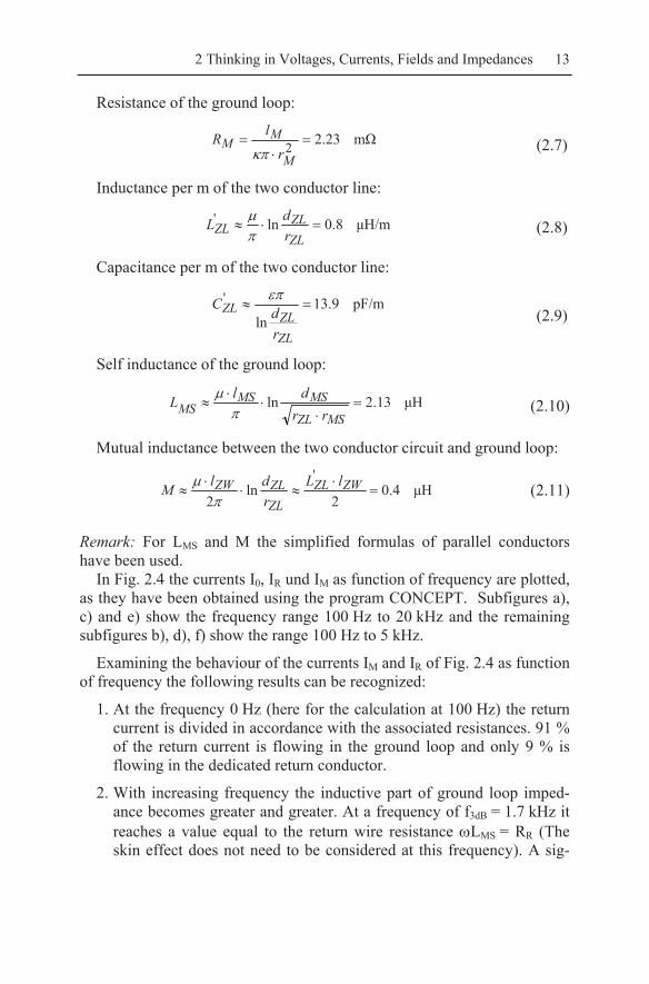
2 Thinking in Voltages, Currents, Fields and Impedances 13
Resistance of the ground loop:
mΩ23.22 =⋅
=M
MM
rlR
κπ (2.7)
Inductance per m of the two conductor line:
μH/m8.0ln' =⋅≈ZLZL
ZL rdL
πμ (2.8)
Capacitance per m of the two conductor line:
pF/m9.13ln
' =≈
ZLZL
ZL
rdC επ
(2.9)
Self inductance of the ground loop:
μH13.2ln =⋅
⋅⋅
≈MSZL
MSMSMS rr
dlLπ
μ (2.10)
Mutual inductance between the two conductor circuit and ground loop:
μH4.02
ln2
'=
⋅≈⋅
⋅≈ ZWZL
ZLZLZW lL
rdlM
πμ (2.11)
Remark: For LMS and M the simplified formulas of parallel conductors have been used.
In Fig. 2.4 the currents I0, IR und IM as function of frequency are plotted, as they have been obtained using the program CONCEPT. Subfigures a), c) and e) show the frequency range 100 Hz to 20 kHz and the remaining subfigures b), d), f) show the range 100 Hz to 5 kHz.
Examining the behaviour of the currents IM and IR of Fig. 2.4 as function of frequency the following results can be recognized:
1. At the frequency 0 Hz (here for the calculation at 100 Hz) the return current is divided in accordance with the associated resistances. 91 % of the return current is flowing in the ground loop and only 9 % is flowing in the dedicated return conductor.
2. With increasing frequency the inductive part of ground loop imped-ance becomes greater and greater. At a frequency of f3dB = 1.7 kHz it reaches a value equal to the return wire resistance ωLMS = RR (The skin effect does not need to be considered at this frequency). A sig-

14 2 Thinking in Voltages, Currents, Fields and Impedances
nificant proportion of the return current is now flowing via the dedi-cated return conductor.
3. With further increasing frequency the inductive reactance of the ground loop becomes higher and higher. The result is that the total re-turn current is now flowing via the dedicated return conductor. How-ever, due to the mutual inductance M between the two conductor cir-cuit and the ground loop, a current in the ground loop will occur. The effect of this is that the measurable return current will be reduced to
⎟⎟⎠
⎞⎜⎜⎝
⎛−⋅≈
MSR L
MII 10 . (2.12)
In the ground loop a current of MS
MS LMII ⋅≈ 0 is flowing.
Taking I0 = 1 V/240 Ω = 4.2 mA and M/LMS = 0.19 results in a measur-able current in the dedicated return wire of IR = 3.4 mA; this result is in very good agreement with the simulation results. In the ground loop a cur-rent of 0.8 mA (for this particular arrangement) is still flowing; it is this current which is the main contributor to the radiation.
It is proposed that a reduction in the ground loop current is required. To do this the mutual inductance M between the two conductor arrangement and the ground loop has to be reduced; in the ideal case it should reduced to zero. This can be achieved by twisting the two conductor line or by us-ing a coaxial cable for the information channel. With respect to the self in-ductance of the ground loop the degree of freedom is very limited. To in-crease the self inductance of the ground loop would mean making the loop size greater, a solution which is contradictory to the requirement of mini-mizing the loop to limit coupling and radiation.

2 Thinking in Voltages, Currents, Fields and Impedances 15
Fig. 2.4 Behaviour of the currents within the two conductor arrangement,
a) and b) forward current I0, c) and d) return current IR, e) and f) ground loop current IM, b), d), f) currents with a zoomed frequency range
Exercises
Exercise 2.1: What is the force (in Newton) that is occurring between the two plates of a capacitor where the plate separation distance is d = 1 mm, the capacitance is C = 1 nF and the capacitor is loaded to a voltage of U = 1000 V?
Exercise 2.2:
a) The shielding of a room against electric fields is realized by the use of wire grids in the ceiling and floor. Between both grids there exists a conducting connection. The diagonal measurement of the grid planes
16 2 Thinking in Voltages, Currents, Fields and Impedances
in the ceiling and floor is D = 10 m, the distance between ceiling and floor is measured to d = 3 m. Up to what frequency is it acceptable to use static field considerations to approximate the shielding effi-ciency?
b) The main board of modern personal computers have dimensions of 30 cm × 20 cm. Up to what frequency might it be acceptable to accu-rately calculate the internal couplings and unwanted interactions on the board by static and stationary field assumptions?
Exercise 2.3: A very long metal plate of a width of b = 10 cm is guiding a current of I = 10 A. How big is the magnetic field strength at a distance of d = 1 cm:
a) away from the edge of the plate,
b) above the middle of the metal plate?
Exercise 2.4: An electron is moving with a speed of vx = 60 000 km/s through a magnetic field of Hz = 2 A/m. How large is the deflection d, per-pendicular to the electron’s initial trajectory, after moving a distance of s = 30 cm?
Exercise 2.5: At a frequency of f = 50 Hz a twisted three conductor cable is producing, at a distance of rM = 10 cm from the cable axis, a magnetic flux density, which can be described by Bϕ = B0 cos (2 π x/SL); where SL = turn width = 0.8 m, B0 = 10 µT. The magnetic flux density is directed perpendicularly into an interference area. The interference area has a radial extension (with respect of the cable axis) of d = 1 cm (starting at r = 9.5 cm) and an axial extension of Δx, starting at x = 0.
a) After what length Δx of the area does the coupling (open circuit volt-age) reach its maximum?
b) How large is the maximum open circuit voltage?
c) After what length Δx of the area does the coupling reach its mini-mum?
Remark: The radial dependence of the field is neglected!
d) The area in which the induction may take place is surrounded by a closed copper wire of a thickness of 2R = 0.4 mm. How large is the current flowing in the influenced wire loop?
e) At what frequency is the resistance of the wire loop equal to the in-ductive reactance (RW = ωL)?

2 Thinking in Voltages, Currents, Fields and Impedances 17
Remark: The self inductance of the influenced loop may be calculated using the relations of a two conductor arrangement.

3 Electric Fields
Electromagnetic fields are described mathematically by the four Max-well’s equations. Expressed in integral form they are:
Ampère’s circuital law
,L Vs A A
H ds J dA D dA I It
∂∂
⋅ = ⋅ + ⋅ = +∫ ∫ ∫ (3.1)
Gauss’ law
,A V
D dA dV Qρ⋅ = ⋅ =∫ ∫ (3.2)
Faraday’s law of induction
∂⋅ = − ⋅ = −
∂∫ ∫s A
E ds B dAt t
∂ φ∂
, (3.3)
0A
B dA⋅ =∫ , (3.4)
H = magnetic field strength, J = current density, D = displacement current density,
LI = conductor current, VI = displacement current,
ρ = charge density, Q = electric charge, E = electric field strength, B = magnetic flux density, φ = magnetic flux,
sd = infinitesimally small element of the contour of area A , Eqs. (3.1) and (3.3).
K.-H. Gonschorek, R. Vick, Electromagnetic Compatibility for Device Design and System Integration, DOI 10.1007/978-3-642-03290-5_3, © Springer-Verlag Berlin Heidelberg 2009
20 3 Electric Fields
These 4 Maxwell’s equations in their integral form can be explained in the following way:
Eq. (3.1): The closed loop integral of the magnetic field strength is equal to the current enclosed by that loop, which is given by the sum of the conductor and the displacement current through the area enclosed by the loop.
Eq. (3.2): The integral of the displacement current density over a closed area is equal to the electric charge enclosed by this area.
Eq. (3.3): The closed loop integral of the electric field strength is equal to the negative time derivative of the magnetic flux flowing through the area enclosed by the loop.
Eq. (3.4): The integral of the magnetic flux density over a closed area is always zero. (i.e. magnetic charges or magnetic monopoles do not exist)
Eq. (3.3), the induction law, is more commonly known in the following form:
tui ∂
φ∂−= , (3.5)
iu = induced voltage.
When assessing electromagnetic incompatibilities it should be noted that the induction voltage given by Eq. (3.5) is only a valid simplification of Eq. (3.3) for the case in which the loop enclosing an area is open at a sig-nal point. At this position in the loop all collected parts of the product
sdE ⋅ are measurable. If the loop has two openings then the external cir-cuitry determines the voltages appearing at the openings. If the loop is closed (short circuited) it must form an induction current which, neglecting the resistance of the loop, produces a magnetic flux equal to the initial flux.
It seems important at this point to mention the fact that Maxwell’s equa-tions, which are the theoretical basis of the electromagnetics, do not ex-plicitly use voltages and potentials.
It has turned out to be very meaningful to divide the electromagnetic fields into:
3 Electric Fields 21
a) Static fields (no time dependence, no current), Maxwell’s equations reduce to
0=⋅∫ sdH , 0=⋅∫ sdE , ∫ ⋅=⋅∫ dVAdDA
ρ and .0=⋅∫ AdBA
(3.6)
Applications: high voltage technology, the effect of voltages and charges, prediction of capacitances, shielding of static electric and mag-netic fields
b) Stationary fields (no time dependence, but currents),
∑=⋅∫=⋅∫ IAdJsdHA
(3.7)
(Ampère’s law in the simplest form), other expressions are the same as in a).
Applications: Prediction of magnetic fields, calculation of self and mu-tual inductances
c) Quasi stationary fields (time dependence with the B -field, cur-rents),
tAdB
tsdE
A ∂∂φ
∂∂
−=∫ ⋅−=⋅∫ (3.8)
(induction law), other expressions are the same as in b).
Applications: Theory of the skin effect, eddy current attenuation
d) High frequency fields (complete set of Maxwell’s equations)
Applications: Electromagnetic wave radiation, electromagnetic cou-pling, antenna theory, shielding theory
Electric fields in the sense of EMC are fields produced by stationary electric charges. If the charges are moving with a low enough speed that the magnetic effects can still be neglected or only a few charged particles are moving (due to circuits with high impedance), then the fields of these charges are still, in the sense of EMC, to be understood and treated as elec-tric fields. In the frequency domain, the boundary between static (station-ary) and non-static is taken at a system extension of l = λ/10; where l is the largest dimension of the arrangement under investigation and λ the wavelength. Electromagnetic incompatibilities at 16 2/3 Hz, 50 Hz or 400 Hz occur either as a result of electric incompatibilities (capacitive in-terferences) or magnetic incompatibilities (inductive interferences, direct or indirect effects of magnetic fields).

22 3 Electric Fields
3.1 Effects of electric fields and their calculation
In chapter 2 it was explained that all electromagnetic phenomena originate from electric charges. Between electric charges force effects occur. Charges with the same polarity repel each other and charges with different polarity attract. This observation leads to the electric field strength E and the electric displacement density D. The electric field strength (as a vector) at a point in space describes the force acting on a charge. An electric field strength of 1 V/m, for instance, applies a force of 1 N on a charge of 1 C. The direction of the vector determines the direction of the force effect. An unbound charge will move as long as the force effect will become zero or a mechanical boundary condition does not allow any further displacement. No electric field strength is possible inside a perfect conductor nor tangen-tially on its surface. Therefore, the condition Etan = 0 (Etan = tangential component) must be fulfilled. This description has been noticeably re-peated here because this association is very helpful in assessing the effects of electric fields. On the body of a car, which is parked under a high volt-age line, 50 Hz currents occur due solely to the electric field. This is due to the restriction that at each point of the surface, at every moment in time, the tangential component of the electric field is zero.
Considering the unchangeable law
2tan1tan EE = (3.9)
where
0tan =E (3.10)
on an ideal conducting metallic surface, many couplings and electric phenomena become apparent.
A lot of practical problems involving the treatment of electric fields do not require predicting the potential distribution (or the distribution of the electric field) when the charge distribution is given. In most cases the in-verse problem has to be solved, where it is necessary to find the charge distribution which leads to a given potential distribution. Subsequently, from this charge distribution the complete field may be predicted. In this manner the problem of predicting the field from given charges is implicitly not a simple task as evaluation of the involved integrals can be difficult. For more details regarding this see annex chapter A1 - solving the problem of finitely long line charges.

3.1 Effects of electric fields and their calculation 23
The inverse problem, predicting the charge distribution when a set of potentials is given, is substantially more difficult and analytical solutions are only given for a limited number of problems. For that reason most real-world problems are only successfully treatable by numerical methods. An often favourable possibility involves applying the charge simulation method. The intrinsic capabilities of this method are scarcely needed for solving problems of electromagnetic compatibility as the method has been proven as very valuable if we restrict ourselves to infinitely and also finitely long line charges. In annex chapter A1.2 a procedure is described for predicting the potential, and also the field strength distribution, within an arrangement of infinitely long horizontal line charges. Then, in annex A1.3 a procedure is described for finitely long vertical rods above a com-mon ground plane. Two simple programs are available (HCOND, VROD) for predicting the fields in arrangements of parallel wires, as described previously. They are also well suited to estimations of the magnitude of the occurring errors. For some simple but obvious examples the application is shown below.
Example 3.1: Next to a residential house, at a distance of 50 m and a height of 10 m, a conductor is installed having a voltage of 10 kV relative to ground. In the house a bedroom is going to be shielded by an arrange-ment of parallel wires.
Fig. 3.1 Shielding of electric fields by an arrangement of parallel wires
To simplify the situation it is assumed that the shielding efficiency for the middle of the room can be approximated by modelling the shielding as an arrangement of very long parallel wires, all having a potential of 0 V. The complete arrangement is shown in Fig. 3.1. To calculate the shielding efficiency the field in the middle of the room (x = 52.5 m, z = 1.25 m) is

24 3 Electric Fields
compared with the value at the same point on the other side of the high voltage line (x = -52.5 m, z = 1.25 m).
Using the program HCOND yields the following result: Ez (52.5 m; 0; 1.25 m) = -0.25 V/m, Ez (-52.5 m; 0; 1.25 m) = -9.2 V/m.
Using the two values obtained above a shielding efficiency of 31.3 dB can be calculated. Taking the arrangement of Fig. 3.1 and using Eq. (7.31) of chapter 7, which is valid for wire meshes (in this case meaning for two parallel arrangements intersecting by 90°), a shielding efficiency of 35 dB is obtained.
Example 3.2: The influence of an additional ground trace on a printed cir-cuit board is to be investigated. The flat tracks are replaced by cylindrical wires. The cross-section of the cylindrical wires is chosen in such a way that they present the same surface as the flat tracks they replaced. For this calculation we assume an effective permittivity of εr = 2.5. Investigated is the capacitive crosstalk between two signal carrying tracks; initially with-out an additional ground track and then with a decoupling ground track lo-cated centrally between the two signal lines.
The starting arrangement is shown in detail in Fig. 3.2a).
Fig. 3.2 Printed circuit board with two parallel signal wires; the thickness of the
signal tracks t = 35 µm and the thickness of the board (of dielectric) h = 1.8 mm, a) starting situation, b) analysed arrangement, c) arrange-ment with the decoupling ground track
The left hand conducting path is excited by a generator with an internal impedance of Ri = 150 Ω and an open circuit voltage of 1 V; the path is terminated by a load impedance of RL = 100 kΩ. The influenced signal track (the second signal line) has, at both ends, an impedance of 200 Ω to ground. An equivalent circuit (mechanical and electrical combination) is shown in Fig. 3.3.

3.1 Effects of electric fields and their calculation 25
U0
R
R
RR
i
C
C
C
L1
L21
L22
10
12
20
Fig. 3.3 Arrangement for studying the coupling between two conductor paths
From the perimeter of the signal tracks the cross sectional area and the radius, r = 0.17 mm, of the replacing cylinders can be calculated. The dis-tance between both conductors is chosen to be 1 mm. The modified ar-rangement is as shown in Fig. 3.2b).
Fig. 3.4 Equivalent circuit for the capacitive coupling between two signal tracks
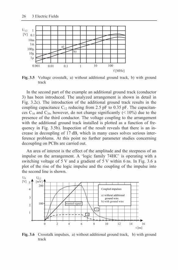
Using the program HCOND for the reconstructed arrangement the fol-lowing stray capacitances can be determined: CL10 = CL20 = 1.27 pF, CL12 = 1.0 pF, which are valid for εr = 1. Recalculating for a relative per-mittivity of εr = 2.5 yields the following quantities: C10 = C20 = 3.2 pF, C12 = 2.5 pF. Together with the chosen source and load impedances and the predicted capacitances it is now possible to construct a complete equivalent circuit for the set up. (See Fig. 3.4). The voltage coupled into the influenced circuit can be calculated using a network simulation pro-gram. The resulting voltage is plotted in Fig. 3.5 where curve a) shows the voltage of interest across RL22 = 200 Ω.
26 3 Electric Fields
Fig. 3.5 Voltage crosstalk, a) without additional ground track, b) with ground
track
In the second part of the example an additional ground track (conductor 3) has been introduced. The analyzed arrangement is shown in detail in Fig. 3.2c). The introduction of the additional ground track results in the coupling capacitance C12 reducing from 2.5 pF to 0.35 pF. The capacitan-ces C10 and C20, however, do not change significantly (< 10%) due to the presence of the third conductor. The voltage coupling to the arrangement with the additional ground track installed is plotted as a function of fre-quency in Fig. 3.5b). Inspection of the result reveals that there is an in-crease in decoupling of 17 dB, which in many cases solves serious inter-ference problems. At this point no further parameter studies concerning decoupling on PCBs are carried out.
An area of interest is the effect of the amplitude and the steepness of an impulse on the arrangement. A ‘logic family 74HC’ is operating with a switching voltage of 5 V and a gradient of 5 V within 6 ns. In Fig. 3.6 a plot of the rise of the logic impulse and the coupling of the impulse into the second line is shown.
Fig. 3.6 Crosstalk impulses, a) without additional ground track, b) with ground
track
3.1 Effects of electric fields and their calculation 27
The increased decoupling observed previously in the frequency range can also be observed in the amplitudes of the impulses. The maximum am-plitudes of the coupled impulses are reduced from 204 mV to 29 mV by the installation of the additional ground trace. Through these results it is entirely conceivable that, by this measure, the internal EMC of the printed circuit board is essentially raised.
In the literature (taken from seminar papers, the original publication could not be recovered until now) for the capacitances between two con-ductor paths on a PCB as shown in Fig. 3.2a) the following equations are stated:
[ ] ( ) pF
th
thh
wmlCC rr
⎪⎪
⎭
⎪⎪
⎬
⎫
⎪⎪
⎩
⎪⎪
⎨
⎧
⎟⎟⎠
⎞⎜⎜⎝
⎛−+
−⋅⋅≈=
142ln
1569
2
22010
εε , (3.11)
[ ] pFdwmlC rrL ⋅⎟
⎠
⎞⎜⎝
⎛ ++⋅⋅≈
214.612
εε , (3.12)
εrL = relative permittivity for the space above the signal tracks, εr = relative permittivity of the PCB material between tracks
and ground.
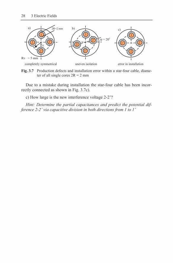
Exercise
Exercise 3.1: Two signal circuits are installed in a star-four arrangement (See Fig. 3.7). As a result of an uneven isolation, two conductors are slightly shifted by an angle of ϕ = 20° out of the symmetry plane. What is the capacitive interference that occurs within circuit 2-2’ if in the circuit 1-1’ a signal voltage of 100 V is used,
a) for the case of complete symmetry (ϕ = 0°)?
b) for the case of an uneven isolation (ϕ = 20°)?
28 3 Electric Fields
Fig. 3.7 Production defects and installation error within a star-four cable, diame-
ter of all single cores 2R = 2 mm
Due to a mistake during installation the star-four cable has been incor-rectly connected as shown in Fig. 3.7c).
c) How large is the new interference voltage 2-2’?
Hint: Determine the partial capacitances and predict the potential dif-ference 2-2’ via capacitive division in both directions from 1 to 1’

4 Magnetic Fields
It has been mentioned in previous chapters that every current produces a magnetic field around itself. In the field of EMC such a magnetic field is termed a magnetic stray field. In order to take the most appropriate meas-ure against the effects of such stray fields the field properties must be known, predicted or at the very least approximated. Considering an ar-rangement, which contains no material of high permeability, it is possible to generate such an approximation with the required level of accuracy needed for EMC countermeasures by means of suitable stray field com-puter programs or the application of simple equations. If field values are desired near to highly permeable materials measured data needs to be used. In particular cases it can be necessary to produce results with sophisticated programs based on the finite element method. In subchapter 4.1 the effects of magnetic fields are recapped, then in subchapters 4.2 to 4.4 formulas for approximating the fields are presented and finally the application of a stray field computer program is described.
4.1 Effects of magnetic fields
The effects of low frequency magnetic fields may be differentiated into:
a) direct effects: for instance, the unwanted deflection of an electron beam according to the force
( )x ,F q v B= ⋅ (4.1)
b) indirect effects: induction of currents and voltages according to the induction law
.dtdui
φ−= (4.2)
K.-H. Gonschorek, R. Vick, Electromagnetic Compatibility for Device Design and System Integration, DOI 10.1007/978-3-642-03290-5_4, © Springer-Verlag Berlin Heidelberg 2009

30 4 Magnetic Fields
Contrary to the effects a), which are proportional to the magnitude of the magnetic field, effects b) are additionally proportional to the time de-rivative.
The whole spectrum of interferences of computer components caused by low frequency magnetic fields, as well as a discussion of possible counter measures, are summarized in paper [GON88].
At this point only a selection of values are mentioned that cause inter-ference to computer components:
• visible movements of picture points on a monitor screen due to changing magnetic fields (16 2/3 Hz or 50 Hz): 2 A/m
• change of colour on monitors (CRT’s): 20 A/m • interferences during writing to or reading from magnetic storage
media: 500 A/m • unwanted voltage inductions in electrical circuits caused by 50 Hz-
fields 2000 A/m • information changes on magnetic storage media: > 5000 A/m
In this context it is interesting to recognise that it is possible to predict high magnetic stray fields of trolley wires and of other electric appliances by use of a computer or television monitor. They permit prediction with respect to the direction and to the magnitude; with accuracy up to a factor of 2. Knowing the magnitude and also the direction provides the possibil-ity of deducing the source of the field.
1. Magnitude Visible, very slight, difficult to see movements: 1 to 2 A/m Unwanted deflections of d = 1 mm: 10 to 20 A/m
2. Direction According to Eq. (4.1) the force on moving charged particles is propor-tional to the amount of charge, the charge velocity, and the magnitude of the magnetic flux density. The force acts perpendicular to the velocity and also perpendicular to the direction of the magnetic field lines. Recalling that the charge particles in a cathode tube are shot from the cathode at the end of the tube onto the picture screen, 3 possible cases (see Fig. 4.1) can be observed in a rough simplification. Interestingly, a field running parallel to the tube axis produces a spiral-shaped interference curve. This can be explained if one considers the velocity component perpendicular to the axis necessary to produce the picture at the borders and corners of the screen.

4.2 Calculation of magnetic field strength of single and multicore cables 31
B
BB
B B
BF
F
v
v v? ?
Fig. 4.1 Impact of low frequency magnetic fields on monitors
4.2 Calculation of magnetic field strength of single and multicore cables
a) One of the most important formulas of EMC reads
rIH⋅⋅
=πϕ 2
. (4.3)
Through this formula the magnetic field strength produced by a single wire (infinitely long), carrying a current I, is defined. The field strength points in the ϕ-direction and is therefore perpendicularly oriented with respect to the radius vector from the current to the field point. In addi-tion, it is also perpendicular to the axis of the wire. The field orientation can be visualised as the orientation of a right winding screw.
b) Consider an arrangement where the forward and return conductor of an electrical circuit are arranged parallel to each other and their cores are separated a distance d. Then, the field at distance r, where r is consid-erably larger than the core separation, can be approximated by
22 rdIH⋅⋅⋅
≈πϕ (4.4)
with a sufficient degree of precision. The field is decreasing quadrati-cally with increasing distance from the conductors.
c) Arranging the forward and the return conductors in a low stray field where each has 2 cores and ordering the cores in the following se-quence: forward - return - return - forward, a formula of the following form

32 4 Magnetic Fields
3
2
22
rdIH⋅⋅⋅⋅
≈πϕ (4.5)
can be derived. The field decreases cubically with the field point dis-tance. A 1/r3-dependence is also obtained if the cores are arranged in a bundle; with the first layer: forward – return and the second layer: return – forward. If a two-conductor system (one forward and one return core) is arranged above a common ground plane with high conductivity, a 1/r3-dependence is also observed due to the mirror principle.
d) To get a 1/r4-dependence 8 cores have to be used (4 forward and 4 re-turn cores) and if a 1/r5-dependence is necessary 16 cores are needed. Within Fig. 4.2 all respective cases are summarised. A more detailed look at the compensation effects can be found in annex A2.1.
Exercises
Exercise 4.1: A power cable is intended to be installed as a 4 core cable in a low stray field arrangement (Fig. 4.2c). The current within the cable (to-tal current in one direction) amounts to 2000 A.
a) How large is the stray field 2 m away from the cable if the core sepa-ration distance (busbar width) is d = 4 cm?
b) Due to a defective mounting a phase sequence + - +- has been used. How large is the new magnetic stray field at 2 m distance?
Exercise 4.2: In the vicinity of a patient having an ECG (electrocardio-gram) a maximum magnetic stray field of 0.4 µTpkpk at 50 Hz is allowed, according to the German VDE 0107 standard. A supply cable, installed at a distance of 0.8 m, carries a maximum current of 40 A.
What is the maximum possible core separation distance permitted for the power cable if the limit value of VDE 0107 has to be met?

4.2 Calculation of magnetic field strength of single and multicore cables 33
a)
c )1
c )2
d)
b)
r
H
d
II
d
I/4 I/4I/4 I/4I/4 I/4I/4 I/4
I/2 I/2I/2 I/2
d
I/2 I/2I/2 I/2
d
I I
22 rdIH⋅⋅⋅
≈πϕ
3
2
22/4
rdIH
⋅⋅⋅⋅
≈πϕ
3
2
22/4
rdIH
⋅⋅⋅⋅
≈πϕ
4
3
24/21r
dIH⋅⋅⋅⋅
≈πϕ
4
5I dH
2 rϕ⋅∼⋅ π ⋅
rIH⋅⋅
=πϕ 2
Fig. 4.2 Low stray field arrangements of cables

34 4 Magnetic Fields
4.3 Magnetic fields of Geofol1 transformers
A major source of concern are the magnetic fields generated by medium voltage transformers, which are reducing the medium voltage of 10/6 kV to the supply voltage of 400/230 V. Within the planning phase the project engineer should at least be able to make an estimation of the future stray field. The electric power supply of multi-storey buildings, in particular, constitutes a significant difficulty and concern today. The medium voltage transformers are, in many cases, installed in the basement of the house. Prior to the existence of TV and computers their fields did not cause any harm to the residents. With ever increasing use of electron beam monitors more and more interference and complaints have been recorded.
In order to estimate the magnetic fields from transformers, specifically Geofol transformers (dry transformers), a formula has been empirically developed from numerous measurements by the Siemens company. The formula has proven to be of great value and is given as:
2
5.0max ][5.0
630][
%6[%]
⎟⎟⎠
⎞⎜⎜⎝
⎛⋅⋅⋅=
mrm
kVAkVAPu
HH nennkurz (4.6)
H0.5 = amplitude of the magnetic field strength at 0.5 m distance from the surface of the transformer,
ukurz = impedance voltage specified in %, Pnenn = rated power in kVA, r = distance from the surface of the transformer in m.
If there is no measured value of H0.5 available, a first order approxima-tion of 100 A/m should be chosen.
A transformer, for instance, having a rated power Pnenn of 200 kVA and an impedance voltage ukurz of 6 % is producing a magnetic field strength Hmax = 2 A/m at a distance r of 2.5 m. This value then has to be compared with the susceptibility values, as specified in chapter 4.1.
When using this equation, it has to be considered that in many cases the busbars bearing the current are producing a higher field. Therefore, in or-der to evaluate the whole situation it is necessary to consider both the field of the transformer and the fields of the busbars (chapter 4.4). In many cases a solution of the interference problem is still reached by installing the busbars closer together (compensation) or installing them on the floor instead of the ceiling or vice versa.
1 Geofol = Siemens trade mark, cast resin dry type transformers

4.4 Magnetic stray fields of arbitrary arrangements of thin wires 35
Exercise
Exercise 4.3: a) What is the magnetic field strength produced by a Geofol trans-
former, having the following parameters: ukurz = 4 %, Pnenn = 100 kVA, at a distance of r = 3 m?
b) Attempt to provide an explanation as to why the field is not depend-ent on the load condition of the transformer in a first order approxi-mation?
4.4 Magnetic stray fields of arbitrary arrangements of thin wires
A finitely long straight wire, running along the y-axis from y = 0 and reaching up to y = a, bearing a current I, is producing a magnetic field strength in the xy-plane which can be calculated by the following equation (Please see annex chapter A2.2 and more specifically A2.6):
.))(
(4 2222 ze
yxxy
ayxxayIH
+−
−+
−=
π (4.7)
The underlined (complex) quantities point to the fact that the phase of the current is transformed into the phase of the field. Through use of this equation and some coordinate transformations, realised by a computer program, it is possible to predict magnetic fields of nearly any arbitrarily orientated and arranged thin wires. In annex A2.2.4 some arrangements are investigated with the help of the program STRAYF, which is available on the web site of the authors. Displayed is the magnetic flux density B, which is easily scaled to obtain the magnetic field strength H (B = μH). It is possible to calculate the magnetic flux densities of single electrodes, trains of straight wires (polygons), windings and twisted cables. Further-more, it is possible to also calculate the magnetic flux density of an arbi-trary combination of all of these elements.
4.4.1 Magnetic field of a four conductor arrangement
In order to demonstrate once again the importance of the phase sequence, two four conductor arrangements are investigated. In the following exam-ple the arrangements are investigated using the program described in an-
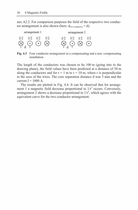
36 4 Magnetic Fields
nex A2.2. For comparison purposes the field of the respective two conduc-tor arrangement is also shown (here: dtwo conductor = d).
d
I/2 I/2I/2 I/2
d
I/2 I/2I/2 I/2
arrangement 1 arrangement 2
Fig. 4.3 Four conductor arrangement in a compensating and a non -compensating
installation
The length of the conductors was chosen to be 100 m (going into to the drawing plane), the field values have been predicted at a distance of 50 m along the conductors and for r = 1 m to r = 10 m, where r is perpendicular to the axes of the wires. The core separation distance d was 5 mm and the current I = 1000 A.
The results are plotted in Fig. 4.4. It can be observed that for arrange-ment 1 a magnetic field decrease proportional to 1/r3 occurs. Conversely, arrangement 2 shows a decrease proportional to 1/r2, which agrees with the equivalent curve for the two conductor arrangement.

4.4 Magnetic stray fields of arbitrary arrangements of thin wires 37
B[µT]
10-1
10-2
10-3
10-4
10-5
1
r[m]104 72 5 83 6 91
Arrangement 2 and two-wires arrangement
Arrangement 1
Fig. 4.4 Magnetic fields of different four conductor arrangements
4.4.2 Magnetic fields of twisted cables
In order to reduce the coupling into a (two conductor) cable, or equally the coupling out of a (two conductor) cable, twisting of the cores has turned out to be a proven measure. The forward and return cores are twisted around each other in such a way that an arrangement consisting of two long, stretched, interwoven windings is created. For a twisted cable a so-called core radius is defined. This is the radial distance from the geometri-cal centre of the twisted cable to the axis of the single cores. The core ra-dius is determined primarily by the insulation of the single cores and their stiffness. To a first order approximation the core radius is given by the thickness of the insulation combined with the radius of the single core. Furthermore, a turn width or turn length (SL) is defined where this is the length of cable over which a complete turn of a core around the imaginary cable axis (3600) takes place. Communication cables typically have a turn length of about 0.1 to 0.2 m, power cables of about 0.8 to 1.2 m.

38 4 Magnetic Fields
The calculation of the magnetic fields of twisted cables is best per-formed by an appropriate computer program. With the already mentioned program STRAYF, for which the source code is available on the home page of the authors and which is described in detail in annex A2.2, the magnetic stray fields of twisted cables are predictable. The necessary equa-tions and relations for writing such a program are given in annex chapter A2. Using the basic approach whereby a helix of a core is represented by a polygon reduces the problem to a geometrical evaluation.
Extensive investigations with respect to magnetic stray fields of twisted cables as well as the coupling of these fields into twisted and untwisted two-wire cables are described in [GON85].
Remark: Calculations with respect to twisted cables can only show trends, because
a) the start angle of twisting is more or less arbitrary, b) the twisted cable must have junctions to circuits or other cables, and c) twisting is not non-ambiguous.
Twisted cables are produced in practice by a so-called pendular stroke. Pendular stroke means mechanically twisting a set of originally parallel wires using a device that grips the bundle of parallel wires and turns them through a predetermined number of turns. Afterwards, the cable is passed through the device by a fixed length and the turning procedure starts again with a reverse turning direction.
In order to show graphically the influence of twisting, the magnetic fields of four two conductor cables are compared in Fig. 4.5. The current is equal to I = 1 A in all cases. The core radius was chosen to be R = 1.5 mm in all four cases. The results have been taken for turn width lengths of 10 cm, 30 cm, 90 cm and infinity (untwisted).
Presented are the magnitudes of the magnetic flux density on a field line perpendicular to the cable axes for a radial distance of r = 0.01 m to r = 1 m.

4.4 Magnetic stray fields of arbitrary arrangements of thin wires 39
Fig. 4.5 Magnetic fields for twisted cables with a core radius of 1.5 mm and a
current of 1 A; fields are calculated on defined field lines perpendicular to the cable axes. Results are shown for: a) turn width SL = 0.1 m, b) turn width SL = 0.3 m, c) turn width SL = 0.9 m, d) untwisted two conductor wire
4.4.3 Example calculation with the program STRAYF
The purpose of the following example (magnetic field of a twisted cable) is to demonstrate the use of the program discussed in annex chapter A2.2 and aid the reader in performing their own calculations. The following subchapter describes some further investigations into the behaviour of twisted cables.
The parameters of the cable under investigation are: total length: 2 m turn width (SL): 25 cm 3 cores, core distance (double core radius): 4 mm currents: I1 = 10 A, 0°, I2 = 10 A, 120°, I3 = 10 A, 240°A
Two cases are investigated:
a) magnetic field on the axis of the twisted cable: results in Table 4.1,
b) magnetic field at 1 cm radial distance from the cable axis: results in Table 4.2.

40 4 Magnetic Fields
Table 4.1 Magnetic field on the axis of a twisted cable Field line 1 -------------
XA BXR BXI BYR BYI BZR BZI BB(μT) 0.75 -6.5E-07 -1.1E-06 -1.5E+02 +3.9E-06 +9.7E-06 -1.5E+02 +1.5E+02 0.78 -5.7E-08 -4.2E-07 -1.2E+02 +9.7E+01 -9.7E+01 -1.2E+02 +1.5E+02 0.81 -2.1E-06 -5.9E-07 -2.6E+01 +1.5E+02 -1.5E+02 -2.6E+01 +1.5E+02 0.83 +1.0E-06 -1.2E-06 +7.4E+01 +1.3E+02 -1.3E+02 +7.4E+01 +1.5E+02 0.86 +2.1E-07 -2.5E-06 +1.4E+02 +5.2E+01 -5.2E+01 +1.4E+02 +1.5E+02 0.89 -2.2E-06 -1.3E-06 +1.4E+02 -5.2E+01 +5.2E+01 +1.4E+02 +1.5E+02
0.92 +9.2E-07 -1.8E-06 +7.4E+01 -1.3E+02 +1.3E+02 +7.4E+01 +1.5E+02 0.94 +1.4E-06 -1.8E-06 -2.6E+01 -1.5E+02 +1.5E+02 -2.6E+01 +1.5E+02 0.97 -3.2E-07 -9.7E-07 -1.2E+02 -9.7E+01 +9.7E+01 -1.2E+02 +1.5E+02 1.00 +1.2E-06 -7.2E-07 -1.5E+02 +1.2E-04 -1.2E-04 -1.5E+02 +1.5E+02 1.03 +1.3E-06 +2.5E-07 -1.2E+02 +9.7E+01 -9.7E+01 -1.2E+02 +1.5E+02
1.06 +1.3E-06 +3.0E-07 -2.6E+01 +1.5E+02 -1.5E+02 -2.6E+01 +1.5E+02 1.08 +2.6E-06 +2.7E-06 +7.4E+01 +1.3E+02 -1.3E+02 +7.4E+01 +1.5E+02 1.11 +1.7E-06 +9.0E-07 +1.4E+02 +5.2E+01 -5.2E+01 +1.4E+02 +1.5E+02 1.14 +9.8E-08 +1.7E-06 +1.4E+02 -5.2E+01 +5.2E+01 +1.4E+02 +1.5E+02 1.17 +3.1E-06 +2.3E-08 +7.4E+01 -1.3E+02 +1.3E+02 +7.4E+01 +1.5E+02 1.19 +1.4E-06 +2.1E-06 -2.6E+01 -1.5E+02 +1.5E+02 -2.6E+01 +1.5E+02 1.22 +8.8E-07 +1.6E-06 -1.2E+02 -9.7E+01 +9.7E+01 -1.2E+02 +1.5E+02 1.25 +3.2E-06 +1.6E-06 -1.5E+02 +2.4E-04 -2.3E-04 -1.5E+02 +1.5E+02
Table 4.2 Magnetic field of a twisted cable on a field line parallel to the cable axis at 1 cm distance from the cable axis
Field line 2 ------------- XA BXR BXI BYR BYI BZR BZI BB(μT) 0.75 +2.7E-01 -1.4E+00 -6.3E+00 +1.3E+00 -1.1E+00 +5.6E+00 +7.2E+00 0.78 -8.8E-01 -7.8E-01 -5.9E+00 +4.1E+00 +3.4E+00 +3.2E+00 +7.3E+00 0.81 -1.7E+00 -1.7E-01 -1.5E+00 +5.0E+00 +6.6E+00 +6.1E-01 +7.0E+00 0.83 -1.3E+00 +4.7E-01 +4.2E+00 +4.8E+00 +5.4E+00 -1.9E+00 +7.2E+00 0.86 -2.4E-01 +1.2E+00 +6.5E+00 +3.0E+00 +1.1E+00 -4.5E+00 +7.3E+00 0.89 +6.9E-01 +1.5E+00 +5.1E+00 -1.2E+00 -2.8E+00 -6.1E+00 +7.0E+00 0.92 +1.1E+00 +9.3E-01 +2.0E+00 -6.1E+00 -4.3E+00 -3.8E+00 +7.2E+00 0.94 +1.1E+00 -3.7E-01 -6.4E-01 -7.2E+00 -4.4E+00 +1.3E+00 +7.3E+00 0.97 +9.8E-01 -1.4E+00 -3.6E+00 -3.8E+00 -3.8E+00 +5.4E+00 +7.0E+00 1.00 +2.7E-01 -1.4E+00 -6.3E+00 +1.3E+00 -1.1E+00 +5.6E+00 +7.2E+00 1.03 -8.8E-01 -7.8E-01 -5.9E+00 +4.1E+00 +3.4E+00 +3.2E+00 +7.3E+00 1.06 -1.7E+00 -1.7E-01 -1.5E+00 +5.0E+00 +6.6E+00 +6.1E-01 +7.0E+00 1.08 -1.3E+00 +4.7E-01 +4.2E+00 +4.8E+00 +5.4E+00 -1.9E+00 +7.2E+00 1.11 -2.4E-01 +1.2E+00 +6.5E+00 +3.0E+00 +1.1E+00 -4.5E+00 +7.3E+00 1.14 +6.9E-01 +1.5E+00 +5.1E+00 -1.2E+00 -2.8E+00 -6.1E+00 +7.0E+00 1.17 +1.1E+00 +9.3E-01 +2.0E+00 -6.1E+00 -4.3E+00 -3.8E+00 +7.2E+00 1.19 +1.1E+00 -3.7E-01 -6.4E-01 -7.2E+00 -4.4E+00 +1.3E+00 +7.3E+00 1.22 +9.8E-01 -1.4E+00 -3.6E+00 -3.8E+00 -3.8E+00 +5.4E+00 +7.0E+00 1.25 +2.7E-01 -1.4E+00 -6.3E+00 +1.3E+00 -1.1E+00 +5.6E+00 +7.2E+00

4.4 Magnetic stray fields of arbitrary arrangements of thin wires 41
4.4.4 Peculiarities of magnetic fields of twisted cables
Looking at the magnetic stray fields of twisted cables, some peculiarities can be observed:
1. The magnetic field on the axis of a three phase power cable, which is symmetrically driven, is circularly polarized.
2. Due to compensation effects combined with the twisting of the cable the field magnitude near to the cable decreases significantly. The field decrease is by a much greater degree than that of the untwisted cable. For distances further away from the cable (starting at distances compa-rable to the turn length) the behaviour converges towards that of an un-twisted cable.
3. Examining a four conductor cable, carrying symmetrical three-phase currents, additional zeros in the field can be observed, which are also obtained by measurement. The distance between zeros in the axial di-rection corresponds again with the turn length. In Fig. 4.6 the magnetic field of a NYM 4 x 4 - cable above an observation plane is shown.
For more extensive investigations with twisted cables the reference to [GON85] is made.
Fig. 4.6 Magnetic flux density of the power cable NYM 4x4, which is carrying a
symmetrical three phase current of 1 A, the cable is running on the x-axis from x = 0 m to x = 6 m, the diagram starts at r = 0.1 m in radial di-rection

42 4 Magnetic Fields
Exercises
Exercise 4.4: Using the program STRAYF the results of two calculations are to be compared in this example.
1. Calculation: Calculate the field of a twisted cable consisting of two cores using the pro-gram SFELD. The cable has a core radius of 5 mm and a turn length of SL = 40 cm and is carrying a current of 1 A. The total length of the cable l = 2 m.
x
10 cm 20 cm I
I
Fig. 4.7 Rebuilding a twisted cable by rectangular cells with changing face direc-
tion
2. Calculation: The twisted cable has been transformed into a flat construction (as shown in Fig. 4.7). Predict the field of the new flat construction of the cable.
a) The results of both calculations should be plotted in one diagram for a field line of 1 m in length (starting at x = 0) at a distance of 10 cm parallel to the cable axis.
b) How large is the difference D (in dB) between the maximum values of both calculations?
Exercise 4.5: A conductor of finite length on the y-axis (from y1 = 0 to y2 = 2 m) is carrying a current of I = 10 A.
a) Calculate the magnetic field strength at (0.5 m; 1 m; 0) using the Ampère's circuital law (Eq. (4.3)).
b) Calculate the magnetic field strength at (0.5 m; 1 m; 0) using Eq. (4.7).
c) Explain why the results of a) and b) differ from each other. What is the boundary condition that has to be fulfilled in both equations?
d) Up to what distance do the results deviate from each other by less than 1 %?
Exercise 4.6: A lightning strike (maximum strike current I = 100 kA, gra-dient dI/dt = 100 kA/ 8 µs) discharges into the lightning rod of a protection
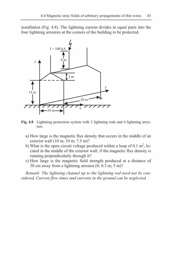
4.4 Magnetic stray fields of arbitrary arrangements of thin wires 43
installation (Fig. 4.8). The lightning current divides in equal parts into the four lightning arrestors at the corners of the building to be protected.
z
y
x10 m
15 m
3 m
20 m
I = 100 kA
6 m
Fig. 4.8 Lightning protection system with 3 lightning rods and 4 lightning arres-
tors
a) How large is the magnetic flux density that occurs in the middle of an exterior wall (10 m; 10 m; 7.5 m)?
b) What is the open circuit voltage produced within a loop of 0.1 m2, lo-cated in the middle of the exterior wall, if the magnetic flux density is running perpendicularly through it?
c) How large is the magnetic field strength produced at a distance of 30 cm away from a lightning arrestor (0; 0.3 m; 5 m)?
Remark: The lightning channel up to the lightning rod need not be con-sidered. Current flow times and currents in the ground can be neglected.

5 Electromagnetic Fields
Electromagnetic fields in the sense of EMC are fields, where the field components electric field strength E and magnetic field strength H cannot be considered independently from each other, but instead have to be treated as mutually dependent fields forming an electromagnetic wave as a result of one field source or one field excitation. Additionally, when con-sidering electromagnetic fields the natural retarding effects (runtime ef-fects), which are described in the frequency domain by phase differences, have to be considered. In vacuum, electromagnetic fields propagate at the speed of light, which is to a good approximation c0 = 3 108 m/s. In dielec-tric material the propagation speed is reduced by the square root of the relative dielectric constant:
.0
r
cvε
= (5.1)
Considering a transmission within a communication line (cable) as an electromagnetic wave it becomes clear that the wave does not propagate with the speed of light, but with a considerably lower velocity. For stan-dard laboratory cable εr = 2.25 is reasonable. Therefore, the propagation velocity is reduced to v = 2/3⋅c0. Hence, in one nanosecond an electromag-netic wave propagates a distance of only 20 cm within a standard labora-tory cable. Reduction of the transmission speed also means that the wave-length within the cable is reduced.
5.1 Characterization of Electromagnetic Waves
An electromagnetic wave has both a temporal and spatial dependence. In Fig. 5.1 wave amplitude is displayed as function of time for the same wave at two different positions.
K.-H. Gonschorek, R. Vick, Electromagnetic Compatibility for Device Design and System Integration, DOI 10.1007/978-3-642-03290-5_5, © Springer-Verlag Berlin Heidelberg 2009
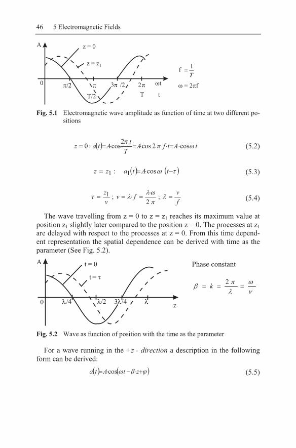
46 5 Electromagnetic Fields
Fig. 5.1 Electromagnetic wave amplitude as function of time at two different po-
sitions
( ) tAtfAT
tAtaz ωππ cos2cos2cos:0 ⋅=⋅⋅=⋅== (5.2)
( ) ( )τω −⋅== tAtazz cos: 11 (5.3)
fvfv
vz
=⋅
=⋅== λπωλλτ ;
2;1 (5.4)
The wave travelling from z = 0 to z = z1 reaches its maximum value at position z1 slightly later compared to the position z = 0. The processes at z1 are delayed with respect to the processes at z = 0. From this time depend-ent representation the spatial dependence can be derived with time as the parameter (See Fig. 5.2).
Fig. 5.2 Wave as function of position with the time as the parameter
For a wave running in the +z - direction a description in the following form can be derived:
( ) ( )ϕβω +⋅−⋅= ztAta cos (5.5)
Phase constant
νω
λπβ ===
2k
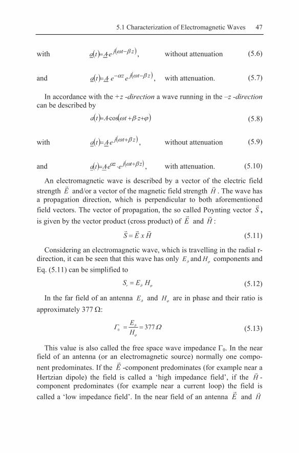
5.1 Characterization of Electromagnetic Waves 47
with ( ) ( )ztjeAta βω −⋅= , without attenuation (5.6)
and ( ) ( )ztjz eeAta βωα −−⋅= , with attenuation. (5.7)
In accordance with the +z -direction a wave running in the –z -direction can be described by
( ) ( )ϕβω +⋅+⋅= ztAta cos (5.8)
with ( ) ( )ztjeAta βω +⋅= , without attenuation (5.9)
and ( ) ( )ztjz eeAta βωα +⋅⋅= , with attenuation. (5.10)
An electromagnetic wave is described by a vector of the electric field strength E and/or a vector of the magnetic field strength H . The wave has a propagation direction, which is perpendicular to both aforementioned field vectors. The vector of propagation, the so called Poynting vector S , is given by the vector product (cross product) of E and H :
HxES = (5.11)
Considering an electromagnetic wave, which is travelling in the radial r-direction, it can be seen that this wave has only ϑE and ϕH components and Eq. (5.11) can be simplified to
ϕϑ HESr = (5.12)
In the far field of an antenna ϑE and ϕH are in phase and their ratio is approximately 377 Ω:
ΩΓϕ
ϑ 3770 ==HE (5.13)
This value is also called the free space wave impedance Γ0. In the near field of an antenna (or an electromagnetic source) normally one compo-nent predominates. If the E -component predominates (for example near a Hertzian dipole) the field is called a ‘high impedance field’, if the H -component predominates (for example near a current loop) the field is called a ‘low impedance field’. In the near field of an antenna E and H

48 5 Electromagnetic Fields
are normally not in phase, resulting in a complex value of the wave imped-ance. These relations are described in more detail in connection with the elementary radiators, which are treated in chapter 5.2.
Electromagnetic waves are differentiated with respect to the common conducting plane into:
a) horizontally polarized waves (Fig. 5.3), The E-vector lies in the reflection plane.
b) vertically polarized waves (Fig. 5.4), The H-vector lies in the reflection plane.
c) elliptically polarized waves (See annex chapter A5). The E-vector consists of 2 or 3 orthogonal components with different phases.
In Fig. 5.3 an electromagnetic wave (horizontally polarized) is shown, which is impinging on a metallic wall at an angle α and which is totally re-flected. The reflection pattern of a standing wave is also shown.
h h
SE
E
H
H
E
S
E
E
E
R
R
R
=
c0
2f
x
h =min
2 cos
E RE = E + E = 0
2 EE
Fig. 5.3 Reflection of a plane wave from a metallic wall (wave with horizontal
polarization)
When measuring electromagnetic fields (with a horizontal polarization) above a reflecting plane it must be considered that such a reflection pattern occurs. The first maximum in the electric field strength can be detected at
αλ
cos4max ⋅=h . (5.14)
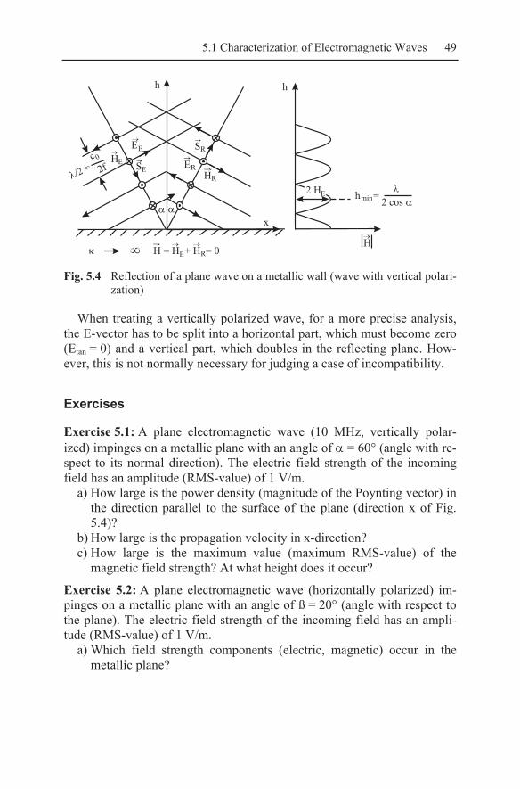
5.1 Characterization of Electromagnetic Waves 49
h h
SH
E
H
S
E
E
E
R
R
=
c0
2f
x
h =min
2 cos
ER
E RH = H + H = 0
2 HE
H
Fig. 5.4 Reflection of a plane wave on a metallic wall (wave with vertical polari-
zation)
When treating a vertically polarized wave, for a more precise analysis, the E-vector has to be split into a horizontal part, which must become zero (Etan = 0) and a vertical part, which doubles in the reflecting plane. How-ever, this is not normally necessary for judging a case of incompatibility.
Exercises
Exercise 5.1: A plane electromagnetic wave (10 MHz, vertically polar-ized) impinges on a metallic plane with an angle of α = 60° (angle with re-spect to its normal direction). The electric field strength of the incoming field has an amplitude (RMS-value) of 1 V/m.
a) How large is the power density (magnitude of the Poynting vector) in the direction parallel to the surface of the plane (direction x of Fig. 5.4)?
b) How large is the propagation velocity in x-direction? c) How large is the maximum value (maximum RMS-value) of the
magnetic field strength? At what height does it occur?
Exercise 5.2: A plane electromagnetic wave (horizontally polarized) im-pinges on a metallic plane with an angle of ß = 20° (angle with respect to the plane). The electric field strength of the incoming field has an ampli-tude (RMS-value) of 1 V/m.
a) Which field strength components (electric, magnetic) occur in the metallic plane?

50 5 Electromagnetic Fields
b) Divide the incoming power density into a component parallel and a component perpendicular to the plane. How large are these compo-nents?
c) What happens to these components within the plane?
5.2 Effects of electromagnetic fields
If an electromagnetic wave is impinging on a metallic, perfectly conduct-ing structure a reflected electromagnetic field is formed. On the surface of the perfectly conducting structure the tangential component of the electric field must become zero, otherwise a very large surface current would flow. Therefore, for the prediction or calculation of high frequency electromag-netic fields generally the boundary condition Etan = 0 is used.
The electromagnetic wave in the far field of an antenna (far away) can normally be considered as a plane electromagnetic wave; E and H are perpendicularly orientated to each other and also perpendicular to S and hence also perpendicular to the propagation direction. If E and H are in phase, their ratio is Γ0 = 377 Ω. Therefore, an electromagnetic wave with S = 2.65 mW/m2 has an electric field strength of
mVSE /10 =⋅= Γ (5.15)
and a magnetic field strength of
./65.2/3771
00mmAmA
SEH ==
Γ=
Γ= (5.16)
If this electromagnetic wave impinges on a metallic wall, it is com-pletely reflected. The reflected electric field strength (to be precise: the horizontal component) ER can be calculated using the E-field reflection co-efficient
0
0
ΓΓΓΓ
+−
=m
mEr (5.17)
with
EER ErE ⋅= . (5.18)

5.2 Effects of electromagnetic fields 51
EE describes the incoming electric field strength and Γm the wave im-pedance of the metallic wall, which is given by
( ) ( )d
jjm κκωμΓ 112
1 ⋅+=⋅+= (5.19)
(ω = 2πf = circular frequency, µ = permeability, κ = conductivity, d = skin depth). For copper at a frequency of 10 kHz, for instance, a very small value of Γm = (1+j) 26.3 µΩ is calculated.
For very small values of Γm Eq. (5.17) can be simplified to
,210Γ
ΓmEr +−≈ (5.20)
yielding a reflection coefficient of:
.22100 ΓκΓκ d
jd
rE ++−≈ (5.21)
The amplitude of the reflected electric field strength is given by EER ErE ⋅= . Taking EE = 1 V/m, copper, and 10 kHz gives
=RE 0.99999986 V/m. This result shows that the assumption of total re-flection of an electromagnetic wave from a metallic surface is valid. Nev-ertheless, for predicting the shielding efficiency of metallic walls this small portion penetrating into the metal is of vital importance. (See chapter 7.4).
It must be remembered: 1.) If an electromagnetic wave impinges on a metallic wall it is almost
completely reflected. 2.) The tangential electrical field strength on a metallic surface is al-
most zero.
In order to obtain a tangential field strength equal to zero, a current in the surface must flow which produces a compensating field that together with the impinging field results in a total field strength of zero.
Considering an electrical installation above an infinitely wide metallic plane, the boundary condition Etan = 0 can be fulfilled by imagining a vir-tual, mirrored arrangement under the plane (mirroring principle).
In Fig. 5.5 a loop and its mirror image is shown. The chosen coordinate system corresponds to the common convention. It can be seen that the cur-rent in +z-direction produce mirror currents also in +z-direction, whereas currents in x- and y-direction reverse their direction.

52 5 Electromagnetic Fields
x
z
y
u
u
u
0
0
0
Z
Z
Z
L
L
L
I
I
I’
I
I
I’
I I
I’
1
2
2
2
3
3
3 1
1
Fig. 5.5 Loop on a conducting ground plane with its mirror image
When analysing arrangements above a common conducting plane using analogous mirror images, it has to be considered that the physical fields only exist in a half-space and are only radiating into a half-space, there-fore:
The capacitance of a rod on a conducting ground plane is double that of a rod in free space with twice its length and a feeding point at the rod cen-tre.
The inductance of a loop on a conducting plane has half the value of the equivalent loop in free space.
A λ/2-dipole in free space has double the radiation resistance (73.2 Ω) compared to a λ/4-monopole above a ground plane (36.6 Ω).
The basic approach of the mirror principle (virtual mirror arrangement under the ground plane) also allows us to calculate
a) the normal component of the electric field on the plane, b) and therefore, the charge distribution within the plane, c) the tangential component of the magnetic field on the plane, d) and therefore, the surface current within the plane.
This idea, that an impinging field is producing a compensating field by itself is very helpful in understanding electromagnetic fields and cou-plings. We consider a rod antenna, which is located within an electromag-netic field with its axis parallel to the direction of the electric field strength. It becomes obvious that a current is flowing on the rod (current distribution), which is compensating the impinging field strength so that it is zero at every position on the surface at all times. If the rod is cut at its midpoint, perpendicular to its axis and a receiver is connected across the slot the effect of the compensation current can be measured, which results in a reception voltage.
5.2 Effects of electromagnetic fields 53
Generally an electromagnetic field has the following effects: 1.) It produces electric currents on metallic structures. 2.) The product of these currents is detectable as a reception voltage. 3.) The electromagnetic field is a carrier of power and energy. 4.) The electric component of an electromagnetic field leads to a
power dissipation density of P/m3 = E2/κ within a lossy dielectric material.
The reciprocity theorem of the electromagnetic technique allows the ar-gument to be reversed:
1. If a high frequency current is flowing on the surface of a metallic body an electromagnetic field is radiated from the surface of the structure.
2. If a metallic structure is excited by a high frequency voltage oscilla-tion then high frequency currents will be produced.
The reciprocity theorem has the important implications: 1. The input impedance of an antenna (or of an arbitrary arrangement)
is the same both for the radiating and for the receiving cases. 2. The antenna diagram is the same both for the radiating and for the
receiving cases.
Electromagnetic fields can be determined analytically from Maxwell’s equations only for very simple arrangements (Hertzian dipole, small cur-rent loop, λ/2-dipole, λ/4-monopole). For that reason problems of practical interest must be solved by approximations or by use of representative com-puter programs for field analysis. In some cases only a measurement on the real system or on a mock-up can bring satisfactory results.
Exercise
Exercise 5.3: A very long conductor (radius R = 1 mm) is installed at a height of h = 10 cm (z-direction) above a conductive plane. The conductor has a voltage of U0 = 10 V compared with the plane and is leading a cur-rent of I = 1 A (running into the picture plane, y-direction).
a) How does the surface charge distribution σ = f(x) look in the plane under the conductor?
b) How does the surface current distribution JF = f(x) look in the plane under the conductor?
c) What are the maximum values of the surface charge and the surface current directly under the conductor?
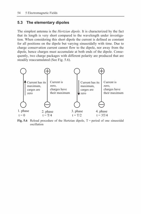
54 5 Electromagnetic Fields
5.3 The elementary dipoles
The simplest antenna is the Hertzian dipole. It is characterized by the fact that its length is very short compared to the wavelength under investiga-tion. When considering this short dipole the current is defined as constant for all positions on the dipole but varying sinusoidally with time. Due to charge conservation current cannot flow to the dipole, nor away from the dipole, hence charges must accumulate at both ends of the dipole. Conse-quently, two charge packages with different polarity are produced that are steadily reaccumulated (See Fig. 5.6).
1. phase 3. phase2. phase 4. phaset = 0 t = T/4 t = T/2 t = 3T/4
Current has itsmaximum,carges are zero
Current has itsmaximum,carges are zero
Current iszero,charges havetheir maximum
Current iszero,charges havetheir maximum
Fig. 5.6 Reload procedure of the Hertzian dipole, T = period of one sinusoidal
oscillation

5.3 The elementary dipoles 55
Fig. 5.7 Electric field of a Hertzian dipoles, shortly before, during, and shortly
after the charges beginning to exchange
Field lines exist between these charge packages, which follow the changes within the packages. Additionally, a radiation process into the sur-rounding space is initiated. In Fig. 5.7 the field diagrams of the electric field are shown for a time step shortly before, during (3rd phase of Fig. 5.6) and shortly after the turning back of the charge packages.
A Hertzian dipole can be approximated by an arrangement consisting of a short rod with two end plates. The dipole is excited through a connection in the middle of the rod as shown in Fig. 5.8.
Fig. 5.8 Practical realisation of a Hertzian dipole
A second very simple antenna configuration is the current loop where the loop radius is small compared to the wavelength. Within the loop a current is flowing, which is constant as function of position and sinusoi-dally varying with time. This current produces a magnetic field, which

56 5 Electromagnetic Fields
again propagates as electromagnetic field into space. The current within the loop forms a virtual magnetic dipole . The field diagrams of the current loop have the same contour structure as the field diagrams of the Hertzian dipole, only the field lines are now representing the H-field. The 1st phase of Fig. 5.6 in relation to the Hertzian dipole has a current of zero within the loop.
z
x
x
r
R
z
x
x
r
I
I
Fig. 5.9 Orientation of the electric and the magnetic dipole
In Fig. 5.9 both elementary dipoles are plotted in their own coordinate system. The directions and component designations used in the following chapters all relate to these coordinate systems.
Remark: The mathematical derivations for the Hertzian dipole and the magnetic dipole (current loop) can be found in annex chapter A4.
The equations of the elementary dipoles are easy to understand and the radiation behaviour of real linear antennas can be derived from the dipole relations. The elementary dipole equations allow an approximation of the field values, both with respect to distance and to the associated compo-nents. Furthermore, the equations are the basis of the shielding theory of Schelkunoff.
For the Hertzian dipole the following equations can be derived in com-plex form:
,2
3
2
2
2sin
2
2ˆ
⎪⎪⎭
⎪⎪⎬
⎫
⎪⎪⎩
⎪⎪⎨
⎧
⎥⎥⎥
⎦
⎤
⎢⎢⎢
⎣
⎡
⎟⎟⎠
⎞⎜⎜⎝
⎛−⎟⎠
⎞⎜⎝⎛−
−⋅=
rrjr
rjelIE
πλ
πλ
πλϑλ
π
εμ
λπ
ϑ (5.22)

5.3 The elementary dipoles 57
,3
2
2
2cos
2
2ˆ2
⎪⎭
⎪⎬
⎫
⎪⎩
⎪⎨
⎧
⎟⎟⎠
⎞⎜⎜⎝
⎛⎟⎟⎠
⎞
⎜⎜⎝
⎛−
−⋅= rj
r
rjelI
rE πλ
πλϑλ
π
εμ
λπ (5.23)
.2
2
2sin
2
2ˆ
⎪⎭
⎪⎬
⎫
⎪⎩
⎪⎨
⎧
⎟⎟⎠
⎞⎜⎜⎝
⎛+
−⋅= rjr
rjelIH π
λπλϑλ
π
λπ
ϕ (5.24)
Dividing Εϑ by Ηϕ yields the so-called radiation impedance (the wave impedance, the field impedance) of the Hertzian dipole:
.0
2
12
220
εμΓ
πλ
πλ
πλ
Γϕ
ϑΓ
=
+⎟⎠⎞⎜⎝
⎛
⎥⎥⎦
⎤
⎢⎢⎣
⎡−⎟⎠
⎞⎜⎝⎛−⎟⎠
⎞⎜⎝⎛
==
jr
rj
r
H
EW
, (5.25)
For the magnetic dipole the following equations can be derived:
,2
22
3
2sin
2
3322ˆ
⎪⎪⎭
⎪⎪⎬
⎫
⎪⎪⎩
⎪⎪⎨
⎧
⎟⎟⎠
⎞⎜⎜⎝
⎛
⎥⎥⎥
⎦
⎤
⎢⎢⎢
⎣
⎡
⎟⎟⎠
⎞⎜⎜⎝
⎛⋅+−
−⋅= rjrr
rjeRIH π
λπλ
πλϑλ
π
λπ
ϑ (5.26)
,2
2
3
2cos
2
3342ˆ
⎪⎭
⎪⎬
⎫
⎪⎩
⎪⎨
⎧
⎟⎟⎠
⎞⎜⎜⎝
⎛⎟⎟⎠
⎞
⎜⎜⎝
⎛⋅+
−⋅= rj
r
rjeRIrH π
λπλϑλ
π
λπ (5.27)
,2
22sin
2
3322ˆ
⎪⎪⎭
⎪⎪⎬
⎫
⎪⎪⎩
⎪⎪⎨
⎧
⎟⎟⎠
⎞
⎜⎜⎝
⎛⋅−⋅
−⋅⋅⋅⋅=
rjr
rjeRIE
πλ
πλϑλ
π
εμ
λπ
ϕ (5.28)
.1
20 2
12 2
jE rW H
jr r
λϕ π
λ λϑπ π
⎛ ⎞⎜ ⎟⎝ ⎠
⎡ ⎤⎛ ⎞ ⎛ ⎞⎢ ⎥⎜ ⎟ ⎜ ⎟⎢ ⎥⎝ ⎠ ⎝ ⎠⎣ ⎦
− ⋅−Γ = = Γ
− − ⋅
(5.29)

58 5 Electromagnetic Fields
In Fig. 5.10 the field impedances of both elementary dipoles are plotted as function of the ratio r/(λ/2π). The field impedance of the Hertzian di-pole in the near field (near to the source) is considerably larger than the free field impedance Γ0 = 377 Ω. Conversely, the field impedance of the magnetic dipole is considerably smaller than Γ0 in the near field. Accord-ingly, the field of the Hertzian dipole is termed a high impedance field and the field of the magnetic dipole, a low impedance field.
Fig. 5.10 Field impedances of the elementary dipoles as function of distance
In the time domain the following equations for the elementary dipoles are applicable:
Hertzian Dipole
( ) ,cos2
2sin2
3
2sin2ˆ
⎪⎪⎭
⎪⎪⎬
⎫
⎪⎪⎩
⎪⎪⎨
⎧
⎟⎠
⎞⎜⎝
⎛⎟⎠⎞
⎜⎝⎛
⎟⎟⎠
⎞⎜⎜⎝
⎛⎟⎠
⎞⎜⎝
⎛⎟⎠⎞
⎜⎝⎛
⎥⎥⎥
⎦
⎤
⎢⎢⎢
⎣
⎡
⎟⎟⎠
⎞⎜⎜⎝
⎛−+−−= v
rtrvrtrr
lItE ωπλωπ
λπλϑε
μλ
πϑ
(5.30)
( ) ,sin3
2cos2
2cos2
ˆ2⎪⎭
⎪⎬
⎫
⎪⎩
⎪⎨
⎧
⎟⎠
⎞⎜⎝
⎛⎟⎠⎞
⎜⎝⎛
⎟⎟⎠
⎞⎜⎜⎝
⎛⎟⎠
⎞⎜⎝
⎛⎟⎠⎞
⎜⎝⎛
⎟⎟⎠
⎞
⎜⎜⎝
⎛−+−= v
rtrvrt
rlItrE ωπ
λωπλϑε
μλ
π (5.31)
5.3 The elementary dipoles 59
( ) ,2ˆ
sin sin cos2 2 2Il r rH t t t
r v r vπ λ λϑ ω ωϕ π πλ
⎧ ⎫⎛ ⎞ ⎛ ⎞⎪ ⎪⎛ ⎞⎛ ⎞ ⎛ ⎞⎨ ⎬⎜ ⎟ ⎜ ⎟⎜ ⎟⎜ ⎟ ⎜ ⎟⎝ ⎠ ⎝ ⎠⎝ ⎠⎝ ⎠ ⎝ ⎠⎪ ⎪⎩ ⎭
−= − + − (5.32)
Magnetic Dipole
( ) ,sin2
2cos2
3
2sin3322ˆ
⎪⎪⎭
⎪⎪⎬
⎫
⎪⎪⎩
⎪⎪⎨
⎧
⎟⎠
⎞⎜⎝
⎛⎟⎠⎞
⎜⎝⎛
⎟⎟⎠
⎞⎜⎜⎝
⎛⎟⎠
⎞⎜⎝
⎛⎟⎠⎞
⎜⎝⎛
⎥⎥⎥
⎦
⎤
⎢⎢⎢
⎣
⎡
⎟⎟⎠
⎞⎜⎜⎝
⎛−−−−= v
rtrvrtrrRItH ωπ
λωπλ
πλϑ
λπ
ϑ
(5.33)
( ) ,sin2
2cos
3
2cos3
342ˆ⎪⎭
⎪⎬
⎫
⎪⎩
⎪⎨
⎧
⎟⎟⎠
⎞⎜⎜⎝
⎛⎟⎟⎠
⎞⎜⎜⎝
⎛⎟⎟
⎠
⎞
⎜⎜
⎝
⎛⎟⎟
⎠
⎞
⎜⎜
⎝
⎛
⎟⎟
⎠
⎞
⎜⎜
⎝
⎛−⋅−⎟
⎠⎞
⎜⎝⎛ −⋅⋅⋅⋅⋅= v
rtrv
rtr
RItrH ωπλω
πλϑ
λπ
(5.34)
( ) .2322ˆ sin cos sin3 2 2
r rE t I R t tr vv r
λπ μ λϑ ω ωϕ ε π πλ
⎧ ⎫⎛ ⎞ ⎛ ⎞⎛ ⎞ ⎛ ⎞⎪ ⎪⎛ ⎞⎨ ⎬⎜ ⎟ ⎜ ⎟⎜ ⎟⎜ ⎟ ⎜ ⎟⎝ ⎠⎝ ⎠ ⎝ ⎠⎝ ⎠⎝ ⎠⎪ ⎪⎩ ⎭
= ⋅ ⋅ ⋅ ⋅ ⋅ ⋅ − + ⋅ −
(5.35)
An important quantity associated with the field equations is the distance r = r0 = λ/2π. It is called the transition distance, or more informally ‚the magic distance’. For distances r considerably smaller than r0 (near to the dipole, near field region) only the terms of the sum with the (r0/r)3- and/or (r0/r)2-dependence are significant. Otherwise, in the far field region only the linear relation r0/r has to be taken into account.
Therefore, in all subsequent evaluations the transition point from near field to far field is fixed to the distance r0 = λ/2π . In near field only power 2 or 3 of the ratio r0/r are taken into account, whereas, in far field only the linear behaviour of r0/r is taken. Furthermore, the field retardations (the time delay between cause and effect) are only considered in the far field equations.
In summary, for the case of the Hertzian dipole the following relations can be stated:
Near field
,3
2sin2
ˆ⎟⎠
⎞⎜⎝
⎛⋅⋅−=r
lIjEπλϑ
εμ
λπ
ϑ (5.36)
,3
2cos2ˆ2
⎟⎟⎠
⎞⎜⎜⎝
⎛⋅⋅−= r
lIjrE πλϑε
μλ
π (5.37)

60 5 Electromagnetic Fields
,2
2sin2ˆ
⎟⎟⎠
⎞⎜⎜⎝
⎛⋅= rlIH π
λϑλ
πϕ (5.38)
.0 2E
jW rHλϑπ
ϕ
⎛ ⎞⎜ ⎟⎝ ⎠
Γ = = − Γ ⋅
(5.39)
Far field
,sin
2
2ˆ
2 r
rjelIjE
πλϑλ
π
εμ
λπ
ϑ ⋅−
⋅= (5.40)
,0=rE (5.41)
,2sin
2
2ˆ
r
rjelIjH π
λϑλπ
λπ
ϕ ⋅−
⋅= (5.42)
.0ΓΓ =W (5.43)
Similarly, for the case of the magnetic dipole the following approxima-tions can be stated:
Near field
,3
2sin3322ˆ
⎟⎟⎠
⎞⎜⎜⎝
⎛⋅= rRIH π
λϑλπ
ϑ (5.44)
,3
2cos3
342ˆ⎟⎟⎠
⎞
⎜⎜⎝
⎛⋅=
rRIrH
πλϑ
λπ (5.45)
,2
2sin3
322ˆ⎟⎟
⎠
⎞
⎜⎜
⎝
⎛⋅⋅⋅⋅⋅−=
rRIjE
πλϑε
μλπϕ (5.46)
.20 ⎟⎠
⎞⎜⎝⎛⋅=
−=
λπΓ
ϑ
ϕΓ rjH
EW
(5.47)
5.3 The elementary dipoles 61
Far field
,2sin2
3322ˆ
r
rjeRIH π
λϑλπ
λπ
ϑ ⋅−
⋅−= (5.48)
,0=rH (5.49)
,2sin2
3322ˆ
r
rjeRIE π
λϑεμλ
π
λπ
ϕ ⋅−
⋅⋅⋅= (5.50)
.0Γϑ
ϕΓ =−
=H
EW
(5.51)
Exercises
Exercise 5.4: Determine the maximum charge occurring at the end of a Hertzian dipole,
a) as an equation, b) as a value for the parameters l = 1 m, f = 1 MHz and Î = 1 A
Exercise 5.5: In the near field of a power loop, with a diameter of 2R = 1 m, an electric field of 1 mV/m is measured at f = 100 kHz. In the plane of the loop the distance between the field point and the middle of the loop is r = 5 m. How large is the current in the loop?
Exercise 5.6: Why is a minus sign introduced into Eq. (5.29), which de-
fines the field impedance of the magnetic dipole, W
EH
ϕ
ϑ
−Γ = ?
5.3.1 Distance conversion
During measuring procedures it is often necessary to perform distance con-versions. The electric field of an EUT, for instance, has been measured at a distance of 3 m. However, the requirement was to measure the field at a distance of 10 m. This introduces the question: How does one convert the 3 m value into a 10 m value? The limit values for radiated emission signals outlined in civilian standards are generally specified for a measuring dis-tance of 10 m, or even 30 m. If a device tested against a civilian limit is

62 5 Electromagnetic Fields
brought into a military environment then the critical distance is reduced. This raises the question: how can we convert the limit values of the 10 m-distance (30 m-distance) to field values at a distance of 1 m. More gener-ally, the question may be expressed as: What is the field strength value ob-tained at a distance r1, if I know the value at a distance r2?
A generally valid statement cannot be delivered. However, a first ap-proximation can be reached by using the equations of the elementary di-poles. It has to be taken into account, however, that these approximations are only valid:
a) for linear antennas ( rod- or whip-antennas), b) for distances larger than the antenna length.
For aperture antennas (slot, face or surface antennas) other distance laws have to be taken into account. Furthermore, as it is normally not known how an EUT radiates, or which part of the EUT is responsible for the ra-diation, a general distance conversion is problematic. The CISPR-approach is to allow measurements at a smaller distance but require that the 10 m limits are met. This approach, however, seems to be rather strict, but this is not without a valid reason. In most cases the cables and lines are radiating, but in the higher frequency range it cannot be omitted that the whole sur-face is acting like an aperture antenna.
The equations of the elementary dipoles show, for their main component of the field (E for the Hertzian dipole, H for the magnetic dipole), terms in the sum with (r0/r)3 -, (r0/r)2- and (r0/r)-dependencies. A rigorous approach is to assume a (r0/r)3 -dependency up to r = r0 and then, at that point, as-sume the main component exhibits a (r0/r)-dependence. It is then easy to perform a conversion from one distance to another providing the men-tioned conditions are taken into account.
Conversion procedure: 1.) From the frequency of interest the transition distance r0 is calcu-
lated,
fcrππ
λ22
00 == . (5.52)
2.) If both points (distances) are in the near field (r1 < r2) the conver-sion is done by 1/r3,
31
32
21 rrEE ⋅= ⋅ . (5.53)
3.) If both points are in the far field, the conversion is done by 1/r,

5.3 The elementary dipoles 63
1
221 r
rEE ⋅= ⋅ . (5.54)
4.) If one point is located in the far field (r2) and the second point in the near field (r1), the conversion from r2 to r0 takes the form 1/r and from r0 to r1 takes the form1/r3, so that
3
1
0
0
221 ⎟
⎠
⎞⎜⎝
⎛⋅⎟
⎠
⎞⎜⎝
⎛⋅=
rr
rrEE . (5.55)
Example 5.1: At a distance of r2 = 20 m away from an electric source an electric field strength of E2 = 80 dBµV/m at f = 3 MHz was measured. What is the field strength that can be calculated for a distance of r1 = 3 m away from the source?
Solution: A frequency of f = 3 MHz corresponds to a transition distance of r0 = 15.9 m.. Therefore, r2 is in the far field and r1 in the near field. Using the relations discussed in this section yields the result
mVdBmVmmVE /3
1 4.125/873.13
9.159.15
20/10 μ==⎟⎠⎞
⎜⎝⎛⋅⎟
⎠⎞
⎜⎝⎛⋅= . (5.56)
The relations discussed previously can be interpreted graphically in terms of the simplified dipole equations in order to aid understanding. Normalising the field strengths with respect to the field at a distance of 1 m the diagram of Fig. 5.11 can be constructed.
At r = r0 = 1 m a frequency of f = 48 MHz has its transition distance. Therefore, at a frequency of f = 48 MHz all distances r smaller than 1 m are located in the near field (60 dB/log distance) and distances r larger than 1 m are located in the far field (20 dB/log distance). For frequencies smaller than 48 MHz the 1/r-region starts at an accordingly further dis-tance; for f = 10 MHz, for instance, at r = 4.8 m. For frequencies larger than 48 MHz the 1/r-region starts at a closer distance; for f = 1 GHz, for instance, at r = 4.8 cm. The frequency f = 48 MHz, although arbitrary, yields an attractively interpretable diagram.

64 5 Electromagnetic Fields
Fig. 5.11 Diagram for the distance conversion
To perform a distance conversion the following procedure needs to be followed: On the line of the frequency under investigation the field differ-ence Δa in dB is calculated by starting at the distance r1 and running up to the distance r2. Then, using the value of Δa, the converted field strength is calculated through the following equations:
( ) ( ) 2012 10
a
rErEΔ
−⋅= (5.57)
and equivalently
( ) ( ) 2012 10
a
rHrHΔ
−⋅= , (5.58)
( ) ( )12 raraa −=Δ . (5.59)
Example 5.2: At a distance of 100 m the field of an electric antenna is measured to be 40 dBµV/m at a frequency of 10 MHz. For a distance of 3 m the converted field has a magnitude of (See Fig. 5.12):
( ) .7838403 // mVmV dBdBdBmE μμ =+= (5.60)

5.3 The elementary dipoles 65
Fig. 5.12 Diagram for predicting Δa of the aforementioned example
Exercises
Exercise 5.7: At a distance of r1 = 3 m from an electric source an electric field strength of E = 10 mV/m at f = 3 MHz has been measured. What is the field strength that can be calculated at a distance of r2 , where:
a) r2 = 10 m, b) r2 = 25 m?
Exercise 5.8: A source produces, at a frequency of f = 1 MHz, an electric field strength of E = 46 dBµV/m at a distance of r2 = 200 m. It is postulated that the field source is magnetic source.
a) How large is the magnetic field strength at a distance of r1 = 5 m?
The source of the field is identified as a loop with a radius of R = 30 cm. b) How large is the current in the loop?
5.3.2 Field impedances
In Fig. 5.10 the field impedances, as derived from Eqs. (5.25) and (5.29), are shown as a function of distance from the dipoles. It is interesting to note that there exists a region in the vicinity of the magic distance (transi-tion distance) where the field impedance of the Hertzian dipole (high im-

66 5 Electromagnetic Fields
pedance field) is smaller than the impedance of the magnetic dipole (low impedance field) and smaller than 377 Ω. In addition, there exists a region where the impedance of the magnetic dipole is larger than the impedance of the Hertzian dipole and larger than 377 Ω.
This peculiarity in the course of the impedances is not normally consid-ered and not normally needed. Employing again the assumption, that in the near field we use only the terms with the highest power (x = 3 and x = 2 in the ratio (r0/r)x ) and use only the linear terms in the far field yields the re-sult shown in Fig. 5.13. Both the high impedance field and the low imped-ance field have a field impedance of ΓW = Γ0 = 377 Ω from the point r/r0 = 1. With decreasing distance the field impedance of the high imped-ance field increases according to
00 ΓΓ ⋅≈rr
W (5.61)
and the field impedance of the low impedance field decreases according to
00
ΓΓ ⋅≈rr
W . (5.62)
Fig. 5.13 Field impedances of the elementary dipoles
What does knowledge of the features of the field impedances tell us?

5.3 The elementary dipoles 67
Two benefits can be stated: 1.) If the nature of the radiation source (linear antenna, whip, rod or
loop) is known, it is possible to make an approximate conversion between the electric and the magnetic components of the field.
2.) If the nature of the radiation source is not known, it is possible to predict its nature by measuring both components E and H. From knowledge of the source characteristics suitable shielding meas-ures can be derived. Furthermore, whilst searching for the source of interference this information can be of great value.
Example 5.3 (example related to the first point): At a distance of r = 3 m the electric field strength of an electric antenna amounts to 78 dBµV/m at a frequency of f = 10 MHz. What is the amplitude of the magnetic component of the field at this point?
Solution: The transition distance at f = 10 MHz can be calculated as r0 = 4.8 m. Consequently, the ratio of r/r0 at the distance of interest amounts to 0.625. At r/r0 = 0.625 the field impedance of the electrical source has the value ΓW = 600 Ω.
Hence, from this value the magnetic field strength can be calculated to be
( ) mAAVmV dBdBdBmH /// 2256783 μμμμ =−= . (5.63)
Example 5.4 (example related to the second point): Some electronic equipment for military purposes shows a limit overshoot of 15 dB at f = 100 kHz (in the electric field with respect to the standard MIL–STD-461). It is proposed that applying an additional shielding measure could possibly allow the limit value to be met. Which procedure do you recommend?
Solution: At 100 kHz the magnetic field strength should also be measured at a distance of 1 m from the surface of the device using a loop antenna.
If the ratio of E/H is substantially larger than 377 Ω, a high impedance interference source is responsible for the limit overshoot. If no shielding box exists, a metallic housing can be chosen to limit the field radiation (A plastic box with a metallic interior should be sufficient). If a shielding en-closure is already in use then it should be checked for weak bonding or possibly an insufficient cable screen connection.
If the ratio of E/H is smaller than 377 Ω, a low impedance interference source is present. By use of Schelkunoff’s shielding theory (chapter 7.4), a problem tailored shielding box has to be designed and constructed.
68 5 Electromagnetic Fields
Exercises
Exercise 5.9: At a distance of 1 m in front of the screen surface of a radar display monitor, an electric field strength of E = 83 dBµV/m at 22.5 kHz has been measured. How large is the magnetic field strength if it is assumed to be
a) an electric interference source, b) a magnetic interference source?
Exercise 5.10: A shielding box for an electronic device has to be designed. The circuit inside the box is functioning with a clock frequency of 1 MHz. Without a shielding box, an electric field strength of 10 mV/m and a mag-netic field strength of 0.6 µA/m can be measured, both at a distance of 1 m.
a) Do the electronics present an electric or a magnetic interference source?
b) Which universally valid rules can be stated for the construction of the shielding box?
5.4 Effective height, effective antenna area, radiation resistance
In chapter 5.3 the radiation fields of the Hertzian and the magnetic dipole have been discussed.
Often the behaviour (radiation resistance, directivity, effective antenna height, and field strength in main beam direction) of antennas that have a different structure to these dipoles is of interest. The elementary dipoles and their relations form the theoretical basis for the derivation of the re-spective values. In the following table (Table 5.1) a selection of the most common linear antennas and their characteristic values are shown.

5.4 Effective height, effective antenna area, radiation resistance 69
Table 5.1 Characteristic quantities of some important antennas within EMC
The characteristic values of the antennas in this table are explained and
clarified using the examples in the following paragraphs. Directivity D resp. antenna gain Gk:
Maximum of the radiation intensity of an antenna D = Mean value of the radiation intensity
Maximum of the radiation intensity of an antenna D = Radiation intensity of an isotropically radiating antenna
Verbally expressed, the directivity of an antenna is the maximum radia-tion intensity divided by the radiation of an isotropic radiator of the same total radiation power. If a fixed distance in the far field of an antenna is chosen, the directivity can also be explained in the following way: The di-rectivity tells us the factor by which the power radiated by the antenna
70 5 Electromagnetic Fields
must be multiplied so that the relations of the isotropically radiating an-tenna can be used.
The gain Gk is often stated in dB. The relation,
10 logG Dk = ⋅ (5.64)
exists for the commonly assumed case where the losses within the antenna can be neglected.
Example 5.5: The λ/2-dipole has, compared with the isotropically radiat-ing antenna, a gain of
10 log 1.64 2.15 .G dBk = ⋅ = (5.65)
In order to achieve the same field strength using an isotropically radiat-ing antenna as opposed to the λ/2-dipole, in the main radiation direction, the power fed into the isotropically radiating antennas must be higher. In fact the feeding power must be 1.64 times the power fed into the λ/2-dipole.
Effective antenna area Aw :
The effective antenna area Aw of a receiving antenna multiplied by the power density at the position of the antenna,
0
2
21
21
ΓEHES =⋅= (5.66)
(Γ0 = field impedance 377 Ω, E and H as peak values), results in a power, which is the power delivered to a receiver matched to the antenna impedance:
ww AEAHEP ⋅=⋅⋅=0
2
max 21
21
Γ. (5.67)
Maximum power consumption is reached if the receiver input imped-ance is equal to the complex conjugate value of the antenna impedance.
Effective antenna height lw :
The effective antenna height lw is a fictitious quantity, which multiplied by the field strength at the position of the antenna, gives the open circuit volt-age of the antenna

5.4 Effective height, effective antenna area, radiation resistance 71
.ElU wL ⋅= (5.68)
Radiation resistance Rr:
The radiation resistance Rr of a lossless antenna is equal to the real part of the antenna input impedance. It can be used in the same way as a resistor of an arbitrary component:
21 ,2 rP I R= ⋅ ⋅ (5.69)
Î = peak value of feed current causing the radiation.
For a general antenna an equivalent circuit can be created as shown in Fig. 5.14:
l Ew
Z
Z
A
E
Fig. 5.14 Equivalent circuit for a receiving antenna
Assuming the maximum power Pmax available from a receiving antenna is obtained if the input impedance of the receiver ZE is the complex conju-gate (ZE = ZA
*) of the feeding point impedance of the antenna. Then, a re-lation between the effective antenna area, the effective antenna height and the radiation resistance can be stated:
.4
02
r
ww R
lA Γ⋅= (5.70)
Field strength in main beam direction:
The main beam direction is the direction in which the antenna produces the highest field strength values in the far field. For the rod antennas stated above, this direction is the direction perpendicular to the antenna axis. Equivalently, for the loop antenna, the main beam direction is in the direc-tion of the loop area (perpendicular to the normal vector of the area).
AZ = feeding point impedance, input impedance
EZ = receiver input impedance

72 5 Electromagnetic Fields
Some remarks to the prediction of lw and Rr
The quantities lw and Rr can be, as stated before, derived from the equa-tions of the elementary dipoles. In the case of real, centre-fed linear anten-nas the current on the antenna can be approximated as a first order ap-proach by
⎟⎠⎞
⎜⎝⎛ −⋅= zlIzI
22sin)( 0 λπ
(5.71)
(antenna on the z-axis, fed at z = 0).
A thorough derivation of the quantities is complicated. However, to ex-plain the principle: If a short antenna segment dz with a constant current according to Eq. (5.71) over its length is considered, all assumptions of the Hertzian dipole are fulfilled and it simply remains to add all short dipole (dz) contributions, through integration, in the correct way.
Using this procedure the method of gaining the radiation resistance can be obtained:
The power density of the radiation in the far field (magnitude of the Poynting vector) multiplied by an infinitesimal area element must be inte-grated over the surface of a sphere. The result is then divided by the square of the feeding point current to give:
2I
AdS
R spherer
∫ ⋅
= . (5.72)
Derivation of the radar equation
Using the result for the effective antenna area it is easy to derive illustra-tively the radar equation. The radar equation allows a prediction about the interference potential of a source on an appliance.
At a distance r an isotropically radiating antenna produces a radiation density of
rSirab eSer
PS ⋅=⋅= 24π. (5.73)
An antenna having a gain GS produces, in the main beam direction, a ra-diation density SS of
24 rGPS Sab
S π⋅
= . (5.74)

5.4 Effective height, effective antenna area, radiation resistance 73
If a second antenna with an effective antenna area AE is installed at a distance r, the maximum receiving power from the second antenna can be calculated by
ESab
ESEmpf ArGPASP ⋅
⋅=⋅= 24π
(5.75)
and finally, the relation πλ4
2
⋅= EE GA yields
2
4 ⎟⎠⎞
⎜⎝⎛⋅⋅⋅=
rGGPP ESabEmpf π
λ. (5.76)
In order to check the validity of the radar equation two λ/2-dipoles are considered, which are optimally orientated with a separation distance of 100 m. The transmitting dipole radiates with a power of 100 W at 15 MHz. It is required to know the receiving power that can be delivered to a re-ceiver matched to the receiving dipole.
A λ/2-dipole has, according to Table 5.1, an input impedance of Zein = 73.1 Ω. In order to radiate at a power of 100 W an antenna current of I = 1.17 A is needed. This current produces an electric field strength of 0.7 V/m at a distance of 100 m, and therefore a radiation (power) density of 1.3 mW/m2. Multiplying this power density by the effective antenna area (table 5.1), which amounts to AE = 59.9 m2 for the considered λ/2-dipole, yields a receiver input power of PEmpf = 78 mW. Using Eq. (5.76) leads likewise to PEmpf = 78 mW.
Exercises
Exercise 5.11: A Yagi-antenna is specified by the manufacturer to have a gain of 8.2 dBi (Note: The index i points to the fact that the gain is given in relation to an isotropically radiating antenna). The power emitted from the antenna is Pab = 100 W.
a) What is the theoretical electric field strength produced by the antenna at a distance of 2 km?
b) What power has to be used for a λ/2-dipole in order to get the same field strength in its main beam direction (ϑ = 900)?
Exercise 5.12: At the location of a high gain antenna there is a received field strength of Eeff = 100 µV/m. A matched receiver (input impedance matched to the antenna impedance) is fed by the antenna and the input power to the receiver is 100 nW.

74 5 Electromagnetic Fields
How large is the effective area of the antenna?
Exercise 5.13: At the input of a high impedance circuit an interference voltage of USS = 100 mV at f = 550 kHz has been measured using a high impedance voltage probe (10 MΩ, 1 pF). At the location of the circuit an electric field strength of Erms = 1 V/m is measured. How long is the effec-tive antenna length of the cable to the input of the circuit?
Exercise 5.14: A crane together with its boom is forming a receiving loop. a) How large is the effective antenna height of the loop formed by the
crane with its boom for a loop area of A = 10 m2 at a frequency of f = 1 MHz (the mirroring ground plane is neglected)?
b) What is the open circuit voltage if an electric field strength of Eeff = 50 V/m is produced at the position of the crane by a nearby me-dium wave station?
c) Calculate the open circuit voltage via the induction law for the given case!
Exercise 5.15: At what frequency is the open circuit voltage in V of a λ/2-dipole equal to the electric field strength in V/m at the position of the an-tenna?
Exercise 5.16: A medium wave station (f = 980 kHz) is radiating a power of 1 MW. The transmitter mast (h = 30 m) may be treated as a short an-tenna above ground. At a distance of r = 300 m from the antenna there is a motorway.
a) How large is the electric field strength on the motorway? b) Attempt to explain why almost no serious interference occurs in the
vehicles passing by.
Exercise 5.17: An electronic device produces an interference radiation of Pab = 100 µW at f = 100 MHz. At a distance of r = 5 m a broadcast antenna is installed which can be described by a λ/2-dipole. How large is the open circuit voltage coupling into the broadcast antenna, if the interference source has a gain of 1.5 (directivity), compared to an isotropically radiat-ing antenna?
Exercise 5.18: A vertical antenna with mechanical height of h = 10 m above an ideal conducting ground emits a power Pab of 100 W at a fre-quency of f = 2 MHz. The antenna consists of a copper rod with a diameter of 2R = 12 mm. The rod is fed at its base, between the ground and the rod.
a) Calculate the feeding current I0 for the ideal case of a lossless an-tenna.
b) How large are the field strength values E and H at a distance of 10 km?

5.5 Estimating the field strength of aperture antennas 75
c) Describe a method for approximating the losses PV of the antenna. How large are the total losses?
d) Calculate the efficiency %100⋅+
=Vab
ab
PPPη of the antenna.
e) How large is the ratio between the radiated power and the losses (ra-tio between the effective and the reactive power)?
Exercise 5.19: For matched antennas, π-networks are often used with vari-able capacitors to ground and a variable coil between them. In such sys-tems the distance between the plates of the variable capacitors are quite large. Attempt to deliver an explanation.
Exercise 5.20: In a setup consisting of a radiating rod of height h1 = 30 cm above ground an electric field strength of E1 = 1 V/m at f1 = 250 MHz has been measured at a distance of r1 = 5 m. What field strength E2 would be measured for a rod of height h2 = 3 m at f2 = 25 MHz at a distance of r2 = 50 m, if the driving voltage U0 is the same in both cases?
5.5 Estimating the field strength of aperture antennas
Up to now only linear antennas (antenna structures consisting of line ele-ments, rods, wires, cables) have been considered. Frequently the EMC-engineer has to also approximate the field strength values produced by ap-erture antennas.
The estimation of field strength values in the far field is relatively sim-ple if the gain or the beam width of the antenna is known. It is more diffi-cult if predictions are required for the so-called beam forming region. This is the region in which, through constructive and destructive superposition of the single ray paths, the radar beam is formed.
In the following paragraphs some statements and equations are given, which allow an approximate calculation of the near field radiation from aperture antennas.
In general, when treating an antenna, the differentiation has to be made between the near field region, which is called the Fresnel region for aper-ture antennas, and the far field region, which is called the Fraunhofer re-gion. The Fraunhofer region is the region in which the beam is already formed and the simple 1/r-decrease takes place. In the Fresnel region, as mentioned above, interference behaviour can be observed, leading to fa-miliar interference patterns with minima and maxima. For more details on this effect see the attachment A1 of chapter V in [GO/NE93].

76 5 Electromagnetic Fields
5.5.1 Power density and electric field strength in the far field region
In the far field, the region in which the electric and the magnetic field strength are perpendicular to each other and have the same phase angle, the power density S (magnitude of the Poynting-vector) is given by
02 / ΓEHES =⋅= , (5.77)
E and H are RMS values and Γ0 = 377 Ω.
This equation is valid up to a distance from the antenna of
λ
2
0
2 Dr ⋅= , (5.78)
D = diameter of circular aperture antennas, λ = wavelength.
Here, the diameter D must be larger than the wavelength λ. The distance r0 is the transition distance as discussed previously.
For an isotropic spherical radiator, emitting a power P, the power den-sity in the far field is given by
24 rPSi π
= . (5.79)
For an antenna with a gain G the equation is modified to:
24 rGPS
π⋅
= . (5.80)
From the equation above the relation for the far field is
mVGWPmr
E /][][
5.5⋅= . (5.81)
Normally the gain of an aperture antenna is given. If not, however, for a ‘worst-case’-approximation it is possible to calculate the gain from the geometrical area of the antenna. The gain G is dependant on the effective antenna area Ae and the wavelength of the radiated signal:
2
4λ
π eAG ⋅= . (5.82)
The effective antenna area Ae is smaller than the geometrical area A of an aperture antenna. The ratio between the effective area Ae and geometri-cal area is called efficiency factor η:

5.5 Estimating the field strength of aperture antennas 77
AAe η= . (5.83)
Hence, the gain is given by:
2
4λπη AG ⋅
⋅= . (5.84)
Furthermore, for a circular antenna the geometrical area is given by:
4
2DA ⋅=
π . (5.85)
When treating elliptical antennas with the dimensions La and Lb the area A can be calculated using the relation:
4ba LLA ⋅⋅
=π
. (5.86)
Using Eqs. (5.84) to (5.86) an approximation of the gain from the geo-metrical dimensions can be performed. The only difficulty is that a realis-tic value for the efficiency factor must be found. However, as the antenna builder strives to obtain a high antenna efficiency and, for carrying out a ‘worst-case’-approximation, an antenna efficiency of η = 1 should be used if no other value is available. Therefore, it is still possible to estimate the far field radiation from knowledge of the geometrical area and the emitted power.
5.5.2 Power density and electric field strength in the near field region
The near field of an aperture antenna extends from a distance r, where r > D, up to the transition distance r0. Using Eq. (5.78) in conjunction with (5.85) the transition distance can be calculated using:
λ/55.20 Ar ⋅= . (5.87)
On the other hand, for this transition distance r0, the power density can be calculated using Eq. (5.80), so that:
20
0 4 rGPS
π⋅
= . (5.88)
Starting from this relation, an equation for the power density Sn in the near field is stated in [BI/HA59]:
78 5 Electromagnetic Fields
⎥⎦
⎤⎢⎣
⎡−⋅+−⋅⋅= )cos(1(2)sin(211.26
20 ww
ww
SSn , (5.89)
with x
w8π
= and 0rrx = .
The maximum of the function in (5.89) occurs at x = 0.1, which corre-sponds to r = 0.1⋅r0. The maximum power density has the value Sn = 41.3 S0,
Maximum: Sn = 41.3 S0 at r = 0.1 r0.
If the value of the electric field strength is required it can be calculated using
0Γ⋅= nn SE (5.90)
(RMS-value). In Fig. 5.15 the power density normalized to S0 is plotted. The result
shown can be calculated using Eqs. (5.89) and (5.80).
Fig. 5.15 Power density of an aperture antenna as function of distance
In the following paragraphs some calculations are presented, which have been carried out using the program APERTUR, which is available from the authors and printed in the German version of this EMC-book. As input parameters the following quantities are required: the radiated power P, the antenna gain G, the diameter D of the antenna, the frequency f and the dis-tance r from the surface to the field point. The output consists of the elec-tric field strength.
Example 5.6: Inputting a diameter D = 0.4 m (for a circular aperture an-tenna), a gain of G = 2000 (33 dBi), a frequency of f = 12 GHz, a radiated

5.5 Estimating the field strength of aperture antennas 79
power of P = 1 MW, and a distance of r = 2 km. A field strength of E = 122.5 V/m is outputted.
Example 5.7: Using D= 1 m, G = 1000, f =9.8 GHz, P = 1 kW, r = 10 km, yields E = 0.55 V/m.
5.5.3 Description of the program APERTUR
As mentioned above a very simple computer program is available on the homepage of the authors. The theory described in this chapter has been implemented in a small BASIC-program. The far field values may be eas-ily checked using the common formula (5.81). The near field values are obtained from Eq. (5.89) and the transition distance r0 is given by Eq. (5.78).
5.5.4 Program SAFEDIST
Historically the first version of the program APERTUR was developed to answer the question about the safety distance to an aperture antenna. Be-cause it might be of interest for the reader it is printed here, but also avail-able from the homepage of the authors.
10 pi=3.1415926536# 20 key off 30 cls 40 print "Program for calculating the safety distance" 50 print "of aperture antennas" 60 print "copyright: Prof. Dr.-Ing. K. H. Gonschorek" 70 print "*********** Version Jan. 20, 1996 *************" 80 print "=======================================" 90 print "" 100 input "do you need an explanation (y/n)? ",a$ 110 if a$ = "y" or a$ = "y" then gosub 500 120 print 130 input "Pulse peak power in Watt? ",pp 140 print 150 input "Pulse repetition frequency in Hertz? ",fp 160 print 170 input "Pulse duration in seconds? ",t

80 5 Electromagnetic Fields
180 p0 = pp*fp*t 190 print 200 input "Diameter 1 of the antenna in metres? ",d1 210 print 220 input "Diameter 2 of the antenna in metres? ",d2 230 print 240 input "Frequency in GHz? ",f 250 r0=6.66666667#*d1*d2*f 260 print 270 input "Antenna gain as factor? ",g 280 print 290 if g > .5 then goto 350 300 input "Horizontal opening angle (3 db-angle) in degree? ",phi 310 print 320 input "Vertical opening angle in degree? ",theta 330 g= .6*13133*pi/phi/theta 340 print 350 if phi < .5 then phi = 157/sqr(g) 351 input "Allowed radiation density in w/m/m? ",pn 360 print 361 input "Do you wish to consider turning of the antenna (y=1/n=0)?",ent 362 if ent = 1 then pn=pn*360/phi 370 pdr0=p0*g/4/pi/r0/r0 380 r=4.4631*r0/(pn/pdr0+3.4191) 390 rk=.1*r0 400 if r > rk goto 440 401 pn = pn*phi/360 404 rz = 2*p0/pn/pi/pi/d2 405 if ent = 0 then rz = rk 406 print 410 print using "Safety distance rn = ###.## metres";rz 420 print "=======================================" 430 goto 480 440 if r < r0 goto 460 450 r = r0*sqr(pdr0/pn) 460 print 465 print using "Safety distance rf = ###.## metres";r 470 print"=======================================" 480 print 490 end 500 rem subroutine ***explanation***** 510 cls 520 print "This program calculates the safety distance of aperture antennas." 530 print 540 print "After specifying the following characteristics" 550 print" pulse peak power"

5.5 Estimating the field strength of aperture antennas 81
560 print" pulse repetition frequency," 570 print" pulse duration," 580 print" diameter of antenna 1," 590 print" diameter of antenna 2," 600 print" frequency in GHz," 610 print" gain," 620 print" allowed radiation density," 630 print 640 print "the distance will be calculated, where the real radiation density" 650 print "is equal to the allowed, specified radiation density." 660 print 670 print "remarks: 1. If circular antennas are treated diameter 1 of the" 680 print " antennais equal to the diameter 2!" 690 print " 2. If the gain is specified to '0' , the program expects the" 700 print " specification of both opening angles (3 db angles)." 710 print" 720 print "The progamm is based on the theory of Bickmore und Hansen." 730 print 740 print "please press a key!" 750 a$ = inkey$: if a$ = "" then goto 750 760 cls 770 return
Example 5.8: Using Ppeak = 1 kW, frep = 1 kHz, ton = 100ns, d1 = 1 m, d2 = 2 m, f = 12 GHz, G = 1000, Pallowed = 200 W/m2,
yields rsafe = 16 m.

6 The Interference Model
In the analysis of observable or suspected interferences it turns out to be meaningful to go back to the interference model. The interference model consists of an interference source, the coupling path, and the interference victim.
Such an interference model is shown in Fig. 6.1. In this diagram some indications are given as to some general measures that should be taken into account in order to lower the coupling.
Fig. 6.1 Interference model
The transfer of interference signals from the source to the victim may oc-cur via:
• galvanic coupling (via common impedances) • capacitive coupling (via the effect of the electric field)
K.-H. Gonschorek, R. Vick, Electromagnetic Compatibility for Device Design and System Integration, DOI 10.1007/978-3-642-03290-5_6, © Springer-Verlag Berlin Heidelberg 2009

84 6 The Interference Model
• inductive coupling (via the effect of the magnetic field) • electromagnetic coupling
Physically, every coupling occurs due to the electromagnetic field. The classification described here provides a certain order to the huge number of possible coupling paths. These classifications make it easier to detect the coupling that leads to the interference. Typically it is helpful to use an ex-clusion procedure in which, as a first assumption, all possible coupling paths are taken into consideration. Then, step by step, the model is reduced to the point where only a few coupling paths remain to be analysed in more detail.
Three-Step-Procedure 1st Step: When starting an analysis of an actual interference case, nor-
mally only the interference effect is known. Here the task consists of detecting the entry point (the gate) of the interference signal. The inter-ference signal may reach the susceptible electronics via the power sup-ply, the signal lines, via sensors or actuators or may occur due to direct irradiation onto the susceptible electronics. At this point in the analysis the solution can often be found by an exclusion procedure (For in-stance: Interference via the power supply can be excluded in case of a battery powered equipment or direct irradiation can be excluded be-cause of good shielding). The use of the burst generator (generator with multiple steep impulses) is a very helpful piece of equipment in investigating disturbed electronic circuits, especially to find the gate.
2nd Step: If the interference is well defined, permanently occurring or re-producible, the second step involves finding the interference source. For the case of permanently emitting interference sources and known interference effects (1. step), the search is normally not time consum-ing. For the case of interference sources that produce sporadically oc-curring impulses, there is only minimal chance to find the interference source in independent systems when having the switching authorisa-tion. Power supply monitoring devices, which permanently observe the supply voltage, have proven to be very helpful in finding the source of sporadic interference.
3rd Step: If the interference source is found, some considerations and in-vestigations related to the coupling path are possibly necessary. This is always the case when the interference victim has a sufficient immunity (according to a test report or susceptibility tests) and the interference source produces signals within ordinarily expected limits. If there is an incompatibility it can be suspected that an elementary mistake has been made, or a fault has occurred within the cabling or grounding.

6 The Interference Model 85
In order to support these statements, three interference cases are pre-sented, which can be solved via the interference model and examination of all possible interference paths.
Example 6.1 (Source problem): A problem occurred within a data process-ing centre containing 25 computer monitors. A number of picture distur-bances could be observed on the screens in a certain corner of the room.
Interference victim: On the monitors slightly shaking pictures and blurred lines occurred. Interference of this kind corresponds to the impact of unwanted high low-frequency magnetic fields. A measurement at the position of the monitors with a coil and a real time spectrum analyser re-vealed the presence of 50 Hz-fields with magnitudes of 3 to 6 A/m.
Interference source: Low-frequency magnetic fields of this magnitude can only be produced by unsymmetrical currents. These are likely to be produced by medium voltage transformers or by machine-tools. In initial discussions, compensating currents on the neutral wire between two build-ings were suspected to be the source. No apparent interference source could be detected. A power supply cable for an air conditioning system in the cellar room below the data processing centre was located. Estimations revealed that an unsymmetrical current of at least 30 A would have to flow in this cable to produce the measured field at the position of the monitors. In actuality a current of 35 A could be measured. Therefore, the reason for the interference was a defect in the air conditioning device.
Example 6.2 (Victim problem): In an opera house the complete lighting system would sporadically fail (for a period of 2 days and with up to 1 in-terference event a month). The lighting was controlled by a programmed control system, which appeared to be failing. The case was significantly problematic because, during an evening performance, complete temporary darkness could occur. To prevent panic, an enhanced emergency lighting system had to be provided.
Interference victim: After a visual inspection it was suspected immedi-ately that the programmed lighting control system was at fault. The system comprises a great number of sliding potentiometers and it was suspected these were responsible for the fault.
The analogue sliding potentiometers (regulators) were, according to a visual inspection, not very well shielded.
Interference source: The interference source has not been located during the one-day investigations.
Coupling path: A direct irradiation into the analogue control system was expected to be responsible.
Diagnosis: Using a burst generator inside the room containing the regu-lators, field impulses were produced (the output of the burst generator was

86 6 The Interference Model
directly connected to a 2 m long copper strip, spanning the length of the control system at half a metre distance from it). Using these undefined field pulses the complete lighting control system could be brought repro-ducibly to a complete stop. It was not necessary to perform a test conform-ing to standards using direct coupling onto the power or signal lines to produce a complete blackout. It was established that an insufficient immu-nity of the control system was the cause of the lighting failure.
Example 6.3 (Problem in the coupling path): The VLF-reception on a submarine was disturbed. Signal disturbances from the environment could be shown to be independent from the diving depth.
Interference victim: In the VLF-reception (VLF = very low frequency, submarine reception between 20 and 50 kHz) clear signals could be heard in the receiver within a 4 kHz-range, which must have been coming from one of the submarine’s own systems. Furthermore, it could be strongly suspected that the signals were coupling directly into the sensitive antenna.
Interference source: Very quickly the static converter for the propulsion motor, which had a base clock frequency of 4 kHz, was identified as the source of trouble. Switching off the converter confirmed this presumption.
Coupling path: According to the EMC design guidelines for the system, all cables leaving the pressure hull had to be connected circumferentially to ground at their penetration point (by a special cable connection). It was suspected that there was a weak connection at this point. The search for such a fault, although very time consuming, proved to be successful. It transpired that an external module had been welded into the pressure hull. This module had insufficient cable shielding, which led to a signal travel-ling from the interior of the submarine to the outside world. This was the signal that was then being picked up by the VLF-receiver.
Experiences are not easy to communicate, however, as examples: • A period of 30 minutes to produce an interference model may de-
cide between success and failure of an analysis. The model would have to characterise the interference source, the possible coupling paths, and the victim in order to reduce the weak points using an ex-clusion procedure.
• For the case of sporadically occurring interferences, a disturbance account has to be written by the complainant. The account should contain the kind of interference, the time, the climatic conditions and any possible peculiarities at the time of the occurrence.
• Interferences in the lower frequency range (up to 1 MHz), if radio reception interferences are neglected, can often be traced back, with

6 The Interference Model 87
high probability, to conducted interference signals or insufficient or faulty grounding.
• Interferences of electronic circuits in the medium frequency range (from 1 to 100 MHz) only occur near to powerful radio stations. The interference victim must have cables with lengths (λ/4, λ/2), which become effective reception antennas.
• With further increasing frequency (above 100 MHz) an increasing number of construction and shielding issues have to be considered in order to limit the interference emission and to improve the immu-nity.
• Digital circuits are normally only disturbed by conducted signals (transient signals from switching actions, short circuit faults in par-allel power lines, lightning voltages and currents).
• Limit overshoots in the interference current above 1 to 5 MHz indi-cate incorrect filtering or a faulty installation of the filter.
• In the early years of computers electrostatic discharges between the user and the interface components were a big problem.
In order to achieve success in the area of electromagnetic compatibility a knowledge of the absolute height or amplitude of interference signals and sensitivities must be developed. Field magnitudes of 1 to 10 V/m for li-censed radio service transmissions and 1 to 10 µV/m for important receiv-ing signals have to be regarded as absolutely normal. In Fig. 6.2 a situation is depicted including interference emissions and immunities for sinusoidal signals (communication signals).
human beeing
10 kHz to 40 GHz DC to 500 MHz
230 V
12 V
mVE μ1000...1=
mVWPrE ⎥⎦
⎤⎢⎣⎡= 7
mVE 50...1=
mVmE 100...1=
communication unit- transmitters- receiver
electronical appliance
Fig. 6.2 Electromagnetic signals, wanted and unwanted

88 6 The Interference Model
Apart from the values given in Fig. 6.2, which can only be taken as a rough reference point, some knowledge should be available about the sus-ceptibility of electronic circuits to transient interference signals.
As a rough reference point the following should be taken into mind: 1 kV impulse voltage for the burst (fast transients) (pulse trains with steep, consecutive, low energy pulses), and 1 kV impulse voltage for the surge (single high energy pulse with a steepness of approximately 1 µs), and 4-8 kV impulse voltage for the ESD (electrostatic discharge).
Fig. 6.3 shows a plot of the unsymmetrical impulse voltages that may occur in low voltage power supplies.
Presented is the over-voltage frequency, which describes how many over-voltages with a magnitude u > u occur within 1,000 h. According to this plot, in normal low voltage power supply networks, for instance, it must be expected that there will be more than 90 pulses per 1,000 h with a magnitude of more than 1 kV.
5000
1000
1000
100
100
10
2000 3000
H
u
L
N
PE
u/V^
Fig. 6.3 Unsymmetrical over-voltages within low voltage power supplies, de-
picted as the frequency of over voltages H(u > u )/1000 h
In treating continual interferences the strategy shown in Fig. 6.4, as a flow diagram, should be followed.
Within the CENELEC-project 4743 a guideline is developed for detect-ing the source of interference. In this guideline (CLC/prTS 50217 “Guide for in-situ measurements – In-situ measurement of disturbance emission“) procedures are described, and decision diagrams are presented, which aid in the estimation and elimination of an interference situation.

6 The Interference Model 89
START
END
END
yes Disturbancereport
available ?
Analysisingthe disturbance
report
Distubance can be provoked?
Not anEMC-problem!
Appliedsignals within the
normal range?
Report aboutbad immunity
Normal environment,
filters installed?
Additional measuresfor unusual
environment
Improvement of the grounding
measures(shielding)
Improvement ofthe wiring in the system
Interferencestill
given?
Interferencestill
given?
Interferencestill
given?
Carrying outan suscepitility
test
no (less)
Measurement of the environment (power supply, field)
yes
yes
yes yes
yes
yes
Fig. 6.4 Decision diagram for the interference detection
Exercise
Exercise 6.1: Inside a power plant, within a monitoring system, a distur-bance is occurring. The disturbance mostly occurs in the evening hours and is clearly introduced by a temperature sensor. The sensor cable is shielded but the shield is only connected to ground on the electronic cabi-net end. A grounding of the cable shield at both ends is rejected by the pro-duction engineer and not allowed. Replacing the 5.3 m long cable by a ca-ble of 6.5 m length eliminates the interferences. Evaluate the situation.
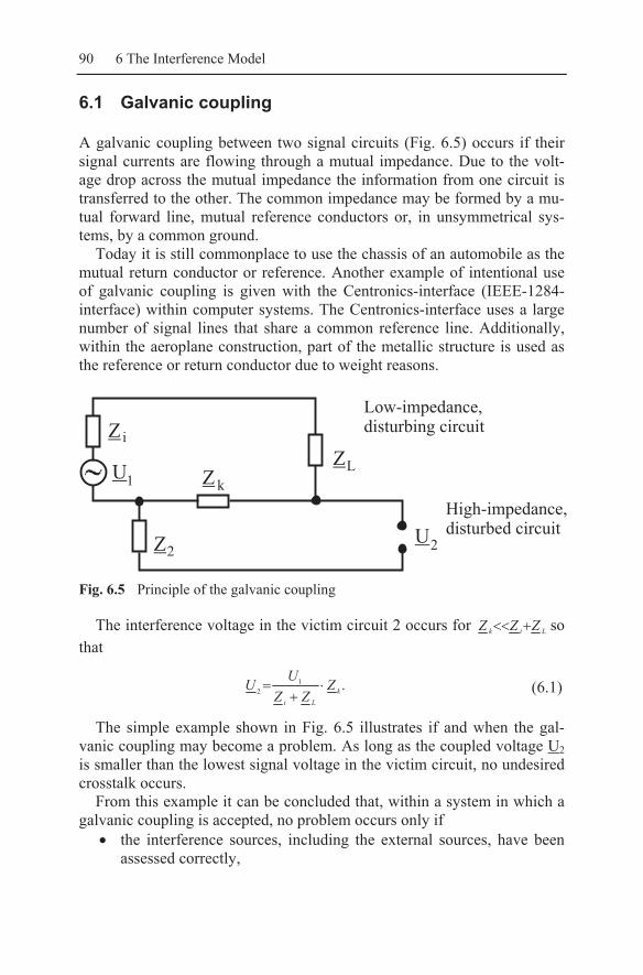
90 6 The Interference Model
6.1 Galvanic coupling
A galvanic coupling between two signal circuits (Fig. 6.5) occurs if their signal currents are flowing through a mutual impedance. Due to the volt-age drop across the mutual impedance the information from one circuit is transferred to the other. The common impedance may be formed by a mu-tual forward line, mutual reference conductors or, in unsymmetrical sys-tems, by a common ground.
Today it is still commonplace to use the chassis of an automobile as the mutual return conductor or reference. Another example of intentional use of galvanic coupling is given with the Centronics-interface (IEEE-1284-interface) within computer systems. The Centronics-interface uses a large number of signal lines that share a common reference line. Additionally, within the aeroplane construction, part of the metallic structure is used as the reference or return conductor due to weight reasons.
Fig. 6.5 Principle of the galvanic coupling
The interference voltage in the victim circuit 2 occurs for Lik ZZZ +<< so that
.12 k
Li
ZZZ
UU ⋅+
= (6.1)
The simple example shown in Fig. 6.5 illustrates if and when the gal-vanic coupling may become a problem. As long as the coupled voltage U2 is smaller than the lowest signal voltage in the victim circuit, no undesired crosstalk occurs.
From this example it can be concluded that, within a system in which a galvanic coupling is accepted, no problem occurs only if
• the interference sources, including the external sources, have been assessed correctly,

6.1 Galvanic coupling 91
• a sufficient signal to noise ratio has been considered, and • everybody is aware of the galvanic coupling when upgrading the cir-
cuit or the system.
When an EMC engineer is planning a system, he requires in a first step that there is a symmetrical signal transmission, in which both signal con-ductors (forward and return conductor) are electrically and geometrically equal with relation to ground. The system requires the same output imped-ances, the same input impedances of both lines with relation to ground.
Fig. 6.6 Crosstalk between 2 signal circuits, which use commonly a reference
conductor, a) measured results, b) setup for measuring the far end voltage
Many unsymmetrical systems only function satisfactorily because the crosstalk signals are detected and eliminated by software measures. The in-terferences are only detectable by the fact that the data rate is decreased.
The impedance, responsible for the coupling (Zk in Fig. 6.5), normally consists of a resistive and an inductive part,

92 6 The Interference Model
LjRZk ω+= . (6.2)
The resistive part is responsible for interference effects in low frequency implementations with very low signal amplitudes (video signals, micro-phone circuits, sonar systems). With increasing frequency resp. increasing steepness of the interference pulses, the inductive part becomes more and more responsible for interferences. Fig. 6.6 shows a diagram illustrating the crosstalk between two circuits where a common reference conductor is used. The inductive coupling, which dominates in this case, could not be eliminated. Nevertheless, the galvanic coupling is easily detectable in the sequence of rectangular pulses, which do not suffer significant deforma-tion.
6.1.1 Measures against a galvanic coupling interference
The measures against galvanic coupling interference can be listed as fol-lows:
1. separation of the ground references (digital, analogue, power sup-ply),
2. limiting the coupling impedances, 3. galvanic decoupling, 4. low impedance construction of the reference conductor (using a ref-
erence plane).
A galvanic decoupling can be obtained using • the electro mechanical principle (relays), • the electro magnetic principle (transformer), • the electro optical principle (optical coupler, fibre optics).
Limiting of the coupling impedances to produce a low impedance con-struction is achieved for the resistive part (R):
• by sufficient large cross sections, • by low impedance transitions at the bounding or connecting points.
for the inductive part (ωL) • by short cable lengths, • cross sections with a high width to thickness ratio (at least 5:1), • small distance between forward and return conductor.
A galvanic decoupling is given if all external peripheral devices are op-erated by 2 wires (cores). This is as a result of the system being a symmet-rically driven system with only one relation to ground at a central point.

6.2 Capacitive coupling 93
The production of a low impedance reference conductor construction can be realised by replacing the reference conductor with a reference plane. In extensive systems and installations all metallic parts should be incorporated into the reference system. All metallic parts should be con-nected to the reference system, wherever possible, and if possible several times.
Furthermore, the attention is discussed in the vast amount of literature regarding galvanic coupling and the construction of the reference conduc-tor system (EMC-lectures at the University of Magdeburg, EMC lecture at the Dresden University of Technology).
Warning!
The single-sided cable connection to ground is able to solve an in-terference problem in particular cases. It is, however, considering the total range of possible interference problems including the limi-tation of the interference emissions, to be rejected as a solution.
Exercise
Exercise 6.2: Two signal loops use a common reference conductor. The conductor consists of a cylindrical copper wire with a radius of R = 1 mm and a length of l = 2 m. In the source loop a current of I = 1 A is flowing.
How large is the coupled open circuit voltage within the victim circuit resulting from only the galvanic coupling at
a) f = 50 Hz, b) f = 500 kHz, c) f = 50 MHz?
6.2 Capacitive coupling
A capacitive coupling occurs if the coupling takes place mostly via the electric field.
Prerequisites for a capacitive interference are: 1. an interference source with rapid high voltage oscillations (conductor
1 against ground in Fig. 6.7), 2. an interference victim with a high impedance load (conductor 2
against ground in Fig. 6.7). For a closer treatment of the capacitive coupling the example from
[GO/SI92, Fig. 1.1-9] is considered again.

94 6 The Interference Model
h1
h2
C20
C10
C12
d
1
2r1
2
22r
2221
'
2221
)(
)(
dhha
dhha
++=
+−=
Fig. 6.7 Capacitive Coupling
Introducing the quantity a as the distance between conductor 1 and con-ductor 2 and a’ as the distance between conductor 1 and the mirrored con-ductor of 2 yields, according to annex A1.2, the following partial capaci-tances:
,'ln2ln2ln
'ln2ln2
2
2
2
1
1
2
2
10
aa
rh
rh
aa
rh
lC−⋅
−= επ (6.3)
,'ln2ln2ln
'ln2ln2
2
2
2
1
1
1
1
20
aa
rh
rh
aa
rh
lC−⋅
−= επ (6.4)
.'ln2ln2ln
'ln2
2
2
2
1
112
aa
rh
rh
aa
lC−⋅
= επ (6.5)
The electrical and geometrical parameters for this example are: U1 = 1 V, f = 1 kHz, h1 = 10 cm, h2 = 10 cm, d = 25 cm r1 = r2 = 6 mm.

6.2 Capacitive coupling 95
From this data the following capacitances per unit length are calculated: C’10 = 14.8 pF/m, C’20 = 14.8 pF/m, C’12 = 1.122 pF/m.
Converting the capacitances of l = 10 m long lines, for example, into impedances, we obtain for f = 1 kHz:
Z10 = Z20 = -j 1.08 MΩ, Z12 = -j 14.2 MΩ.
If the second line is short circuited, a current of
nAjCjUIk 4.70121 −=−= ω
is flowing via the short circuit connection. The quantity 1/(jωC12) gives the inner impedance of the source. If the line, for example, is loaded by a re-sistance RL = 1 kΩ, the current flowing through the load is almost the same as the short circuit current calculated previously. The voltage across the load, on the other hand, becomes very small, where
VjRCjURIU LLkL μω 4.701212 −=−== .
In summary: Within the capacitive coupling very quick very high interference volt-
ages occur. The inner impedance of an electric interference source, which is calculated from the associated capacitances (in many cases from the ca-pacitance between the voltage bearing conductor and the influenced signal line), is generally very high. This results in significant interference volt-ages only within high impedance circuits.
The treatment of the capacitive coupling boils down in nearly all cases to the prediction of stray capacitances. Using the procedure for the ap-proximate determination of electric fields within arrangements of thin elec-trodes (wires, cables, lines, linear antennas), described in annex A1, the capacitances of corresponding arrangements can be calculated.
6.2.1 Measures to lower the capacitive coupling
The following measures can be used to reduce the capacitive coupling: 1.) The source and victim have to be constructed and installed within
the system so that the coupling capacitances are very low. This means: having the maximum possible distance between the de-vices, using of natural shielding, producing a compact construc-tion of the single devices.
2.) The source and/or victim have to be shielded (see chapter 7.2).

96 6 The Interference Model
3.) Problems due to capacitive coupling within the cabling system can possibly be solved by a symmetrical arrangement of the single wires. In Fig. 6.8 the so called star-four-arrangement of four wires be-longing to two circuits is shown. If the voltage ratio between 1 and 1’ via C12’ and C1’2’ is equal to the voltage ratio via C12 and C1’2 , no interference voltage (caused by capacitive coupling) oc-curs within the system 22’. More generally the requirement can be written in the form:
2'112'2'1'12 :: CCCC = (6.6)
4.) The amplitude and steepness of the voltage changes within the dis-turbing system should be kept as small as possible.
5.) The victim system should be assembled with an impedance as low as possible.
1
1’
2 2’
CC
CC
12’12
1’2’1’2
Fig. 6.8 Star-four-arrangement of 4 wires belonging to 2 different circuits
Exercises
Exercise 6.3: The capacitive coupling between two 2-conductor systems (see Fig. 6.9) is to be investigated.
a) Predict the partial capacitances C10’ to C24’ (capacitances per metre, F/m).
b) How large is the voltage U34 in the system 3-4, as a result of the ca-pacitive coupling, if the system 1-2 is operated by a voltage of U0 = 1 kV ( V500± against ground) at a frequency of f = 50 Hz?
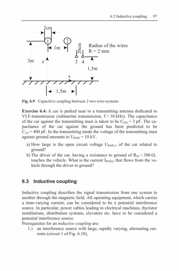
6.3 Inductive coupling 97
z
x1,5m
3m
2cm
1m
1,5m
20cm Radius of the wires
R = 2 mm
1 2
3 4
Fig. 6.9 Capacitive coupling between 2 two-wire-systems
Exercise 6.4: A car is parked near to a transmitting antenna dedicated to VLF-transmission (submarine transmission, f = 18 kHz). The capacitance of the car against the transmitting mast is taken to be CMA = 3 pF. The ca-pacitance of the car against the ground has been predicted to be CA0 = 400 pF. In the transmitting mode the voltage of the transmitting mast against ground amounts to URMS = 10 kV.
a) How large is the open circuit voltage URMS,A of the car related to ground?
b) The driver of the car, having a resistance to ground of RM = 300 Ω, touches the vehicle. What is the current IRMS,F that flows from the ve-hicle through the driver to ground?
6.3 Inductive coupling
Inductive coupling describes the signal transmission from one system to another through the magnetic field. All operating equipment, which carries a time-varying current, can be considered to be a potential interference source. In particular, power cables leading to electrical machines, thyristor installations, distribution systems, elevators etc. have to be considered a potential interference source. Prerequisites for an inductive coupling are:
1.) an interference source with large, rapidly varying, alternating cur-rents (circuit 1 of Fig. 6.10),
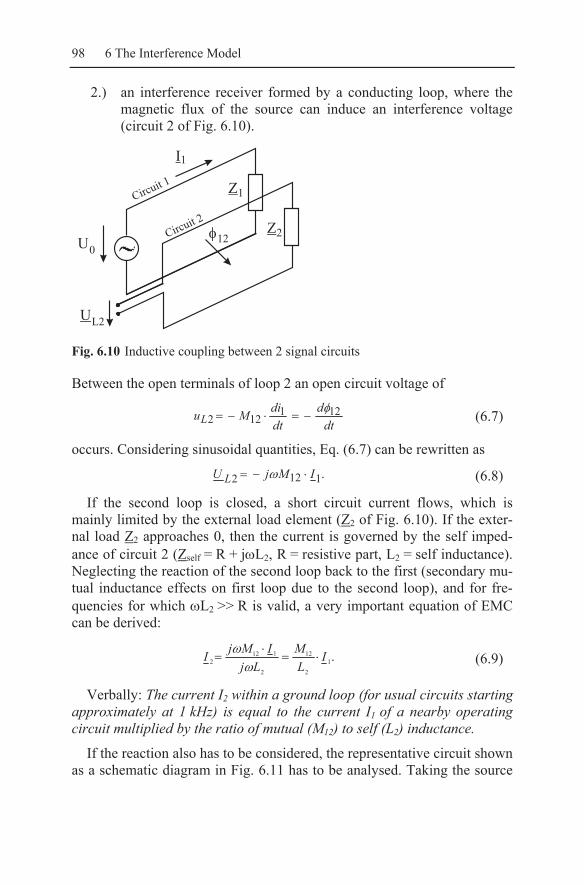
98 6 The Interference Model
2.) an interference receiver formed by a conducting loop, where the magnetic flux of the source can induce an interference voltage (circuit 2 of Fig. 6.10).
Z1
Z2
I1
U0
UL2
12
Circuit
1
Circuit
2
Fig. 6.10 Inductive coupling between 2 signal circuits
Between the open terminals of loop 2 an open circuit voltage of
dtd
dtdiMuL
121122
φ−=⋅−= (6.7)
occurs. Considering sinusoidal quantities, Eq. (6.7) can be rewritten as
.1122 IMjU L ⋅−= ω (6.8)
If the second loop is closed, a short circuit current flows, which is mainly limited by the external load element (Z2 of Fig. 6.10). If the exter-nal load Z2 approaches 0, then the current is governed by the self imped-ance of circuit 2 (Zself = R + jωL2, R = resistive part, L2 = self inductance). Neglecting the reaction of the second loop back to the first (secondary mu-tual inductance effects on first loop due to the second loop), and for fre-quencies for which ωL2 >> R is valid, a very important equation of EMC can be derived:
.12
12
2
1122 I
LM
LjIMjI ⋅=
⋅=
ωω (6.9)
Verbally: The current I2 within a ground loop (for usual circuits starting approximately at 1 kHz) is equal to the current I1 of a nearby operating circuit multiplied by the ratio of mutual (M12) to self (L2) inductance.
If the reaction also has to be considered, the representative circuit shown as a schematic diagram in Fig. 6.11 has to be analysed. Taking the source

6.3 Inductive coupling 99
voltage u0(t) to be sinusoidally varying, the following equations can be de-rived:
1212221122
122110
0,
MjIZIMjIZIMjIZIU
ωωω
⋅−⋅=⋅−⋅=
⋅−⋅= (6.10)
M = M
I2
Z2Z1
I1
U0
12 21
Fig. 6.11 Schematic diagram of the closed loop of Fig. 6.10
Rearranging Eq. (6.10) for I2 yields
21
212
212
1
0
21212
2120
2
ZZM
MjZU
ZZM
MjUI
+
⋅=+
⋅=
ω
ω
ω
ω (6.11)
Assuming Z2 = 0 requires jωL2 to be considered as stated previously. Therefore
.
21
212
212
1
02
LjZM
MjZU
I
ωω
ω
+
⋅= (6.12)
From Eq. (6.12) it can be seen, by comparison with Eq. (6.9), that the reaction from circuit 2 to circuit 1 may be neglected, if the condition
21212
2 LZM ωω ⋅<< (6.13)
is satisfied, which can be assumed in nearly all cases of EMC.
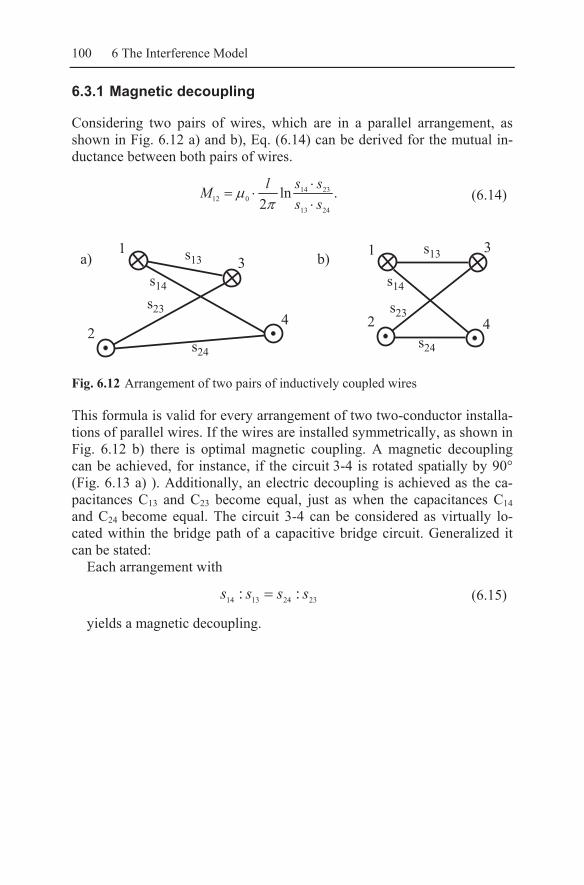
100 6 The Interference Model
6.3.1 Magnetic decoupling
Considering two pairs of wires, which are in a parallel arrangement, as shown in Fig. 6.12 a) and b), Eq. (6.14) can be derived for the mutual in-ductance between both pairs of wires.
.ln2 2413
2314012 ss
sslM⋅⋅
⋅=π
μ (6.14)
1 1
3
3
224 4
ss
s s
s s
s s
1313
2323
14 14
2424
a) b)
Fig. 6.12 Arrangement of two pairs of inductively coupled wires
This formula is valid for every arrangement of two two-conductor installa-tions of parallel wires. If the wires are installed symmetrically, as shown in Fig. 6.12 b) there is optimal magnetic coupling. A magnetic decoupling can be achieved, for instance, if the circuit 3-4 is rotated spatially by 90° (Fig. 6.13 a) ). Additionally, an electric decoupling is achieved as the ca-pacitances C13 and C23 become equal, just as when the capacitances C14 and C24 become equal. The circuit 3-4 can be considered as virtually lo-cated within the bridge path of a capacitive bridge circuit. Generalized it can be stated:
Each arrangement with
23241314 :: ssss = (6.15)
yields a magnetic decoupling.

6.3 Inductive coupling 101
Good Better
Fig. 6.13 Magnetic decoupling
Mechanically and electrically stable relations are obtained if the circuit 3-4 is shifted to the left, up to the point where a symmetrical four conduc-tor arrangement (star-four-arrangement) is formed, as shown in Fig. 6.13 b). In reality a decoupling of 20 to 40 dB is achievable with such an ar-rangement. Furthermore, if the star-four-arrangement is turned or twisted, there is a high decoupling to the electromagnetic environment in addition to the magnetic and electric decoupling of both circuits.
The treatment of the inductive coupling normally demands the predic-tion of self and mutual inductances.
In annex A3 a procedure is described for the approximate prediction of these inductances. A related program called MUTUAL is, both as source code and as an executable, available on the home page of the authors.
6.3.2 Definition of an effective mutual inductance for a multicore cable
In treating the coupling between three-phase arrangements and victim loops it is possible to define a so-called effective mutual inductance of a three-phase system. This quantity considers the phase behaviour of the cur-rents within the geometrical arrangement. In order to illustrate this concept the arrangement of Fig. 6.14 is investigated. As an example, it is required to quantify the coupling into a loop due to a symmetrically driven three-phase supply installed nearby.

102 6 The Interference Model
I = I e
I = I e
I = I e
1
3
2
0
0
0
j0
j240
j120
0
0
0
2
3
1
Fig. 6.14 Defining an effective mutual inductance within three-phase arrange-
ments
In this example, the influenced loop consists of the area between the screen of the three-phase cable and the nearby ground plane.
A mutual inductance can be determined for each phase, leading to the following coupling equation
.00 240
03120
0201jj
i eIMjeIMjIMjU ⋅−⋅−⋅−= ωωω (6.16)
Rearranging this equation to
⎟⎠⎞⎜
⎝⎛ ⋅+⋅+⋅−=
00 2403
120210
jji eMeMMIjU ω (6.17)
yields the definition 0240
3
012021
jjeff eMeMMM ⋅+⋅+= . (6.18)
Taking the relations
235.0
235.0 240120 jeandje jj −−=+−= °° (6.19)
into consideration, the following solution can be derived:
1 2 3 2 3
2 2 21 2 3 1 2 1 3 2 3
1 1 3 32 2 2 2
,
eff
j
M M M M j M j M
M M M M M M M M M e ϕ
= − − + −
= + + − − − ⋅
(6.20)
.2
33arctan321
32
MMMMM
−−⋅−⋅
=ϕ (6.21)

6.3 Inductive coupling 103
If the quantity of interest is the maximum voltage coupling into the loop then the calculation reduces to the prediction of the absolute value of the mutual inductance.
Thus, the induced voltage is now given by
.32312123
22
210 MMMMMMMMMIU i −−−++⋅= ω (6.22)
r
S1
x = 1.50 m x0
y
x
M
[pH]
115
230
345
460
x - 1.50 [m]
0.0 0.1 0.2 0.3 0.4 0.5
*
a)
b)
*
S2
Fig. 6.15 Example for the definition of an effective mutual inductance for
r = 10 cm, S1 = 1 m, S2 = 0.5 m, core radius for both two-wire lines RS = 1 cm
Effective mutual inductances can be defined in all cases in which the phase relations of the interference source are known and the phases of the currents can be factored in the calculation of the mutual inductance. The advantage of the effective mutual inductance quantity becomes apparent when considering the reduction in effort in performing multi-evaluations of a given situation. Furthermore, a greater benefit is that the fundamental inductive behaviour becomes more understandable.
In Fig. 6.15 an example for the behaviour of a mutual inductance be-tween two two-wire lines with different twisting is shown, which has been taken from the publication [GON85].

104 6 The Interference Model
6.3.3 Measures to reduce the inductive coupling
The following measures can be performed to lower the inductive coupling: 1.) Minimize the areas of the conductor loops and/or enlarge the dis-
tance between the interference source and victim. 2.) Magnetic decoupling by a symmetrical arrangement. 3.) Twisting the cores of the conductors, whilst avoiding equal twist
length for cables installed in parallel. 4.) Having increased requirements: applying specific low stray field
requirements. 5.) Avoiding parallel installations of strongly interfering and very
sensitive cables (with relation to the connected circuits). 6.) Keeping the amplitude and steepness of current changes small in
the disturbing system. 7.) Constructing the victim system in a low impedance manner with a
high immunity to interference ratio. 8.) Applying a tailor-made shielding.
Exercises
Exercise 6.5: a) The mutual inductance M between the two two-wire systems, as
shown in Fig. 6.16, has to be predicted (length of the interference sec-tion l = 10 m).
Fig. 6.16 Two inductively coupled two-conductor systems
b) How large is the mutual inductance M between the two circuits if they are installed above a conducting plane, as shown in Fig. 6.17?

6.3 Inductive coupling 105
Fig. 6.17 Two inductively coupled two-conductor systems above a conductive
ground plane
Exercise 6.6: Within the two-conductor system 1-2 of Fig. 6.17 a current of I1 = 10 A is flowing.
a) How large is the short circuit current I2 within loop 3-4 for an inter-ference section length of l = 10 m, if the resistive part of the imped-ance of the loop is neglected?
b) At what frequency fü is the resistive part R34 (κ = 57 106 S/m) equal to the imaginary part ωL34 of loop 3-4?
c) The circuit 1-2 is driven by a generator with in output impedance of 10 Ω. Is it permissible to neglect the reactive effect of loop 3-4 to the circuit 1-2 at f = 10 fü? Justify your answer?
Exercise 6.7: According to Eq. (6.14) the maximum magnetic coupling between two two-wire pairs is given if they are arranged in parallel with a common symmetry plane (Fig. 6.12 b).
a) What additional decoupling (decrease of the mutual inductance) is achieved if the distance s13 = s24 = s is doubled, but keeping the dis-tance d12 = d34 = d constant (as an equation)?
b) The initial distance amounts to s13 = s24 = 10 cm, the core distance is d12 = d34 = 10 cm. How many dB is the coupling between both wire pairs reduced when the mutual distance is doubled to s13 = s24 = 20 cm?
106 6 The Interference Model
6.4 Electromagnetic coupling
By definition, every coupling caused by currents or voltages has to be called an electromagnetic coupling. In order to simplify the electromag-netic interactions, the electromagnetic coupling in this text is describing coupling processes in which the dimensions of the arrangements under in-vestigation are no longer small with respect to the wavelength. The transi-tion between the static or stationary and the high frequency region has been chosen to be l = λ/10, where l is the largest geometrical dimension within the arrangement under consideration (see chapter 2).
If the geometrical dimensions are larger than λ/10 of the frequency of interest the runtime effects, which show up as phase differences in the fre-quency range, can no longer be neglected. Hence, it is no longer satisfac-tory to count on simultaneousness of the electromagnetic actions. A gen-eral procedure to estimate the electromagnetic coupling can no longer be given. In terms of the accuracy required within an EMC-analysis first re-sults and approximations may be derived by use of the antenna theory. First predictions can be made to answer the questions:
• whether a serious danger of a mutual impact via the electromagnetic field is likely or not; or
• whether a disturbance may occur in the radio reception due to inter-ference emissions from electronic devices or not; or
• whether the intended radiation of a licensed radio service may cause faults or interference to electronic devices or not.
A tried and tested means related to the elementary dipoles is the applica-tion of a λ/2-radiator. For both the reception case and for the radiation case simple to understand relations exist. It can be considered that the use of the λ/2-relations may form a ‘worst-case’-assumption. However, using this as-sumption numerical results can be obtained very quickly.
The equations of the λ/2-antenna are given in the following chapter 6.4.2. However, it must be taken into account that in the stated form only predictions for the far field are possible where the condition
“Distance larger than λ/2 (length of the antenna)“
is satisfied.
For structure dimensions smaller than λ/10 the static and stationary as-sumption may be used, so that only an uncertainty for arrangements with dimensions between λ/10 and λ/2 remains. In this range it is suggested that estimations are carried out using both the λ/2-model and the sta-

6.4 Electromagnetic coupling 107
tic/stationary model. The result that shows the larger incompatibility is taken as the suitable approximation.
Remarks: The preceding descriptions have aimed to make the reader aware of
geometrical dimensions, running times and wavelengths, when assessing results. In general, computer programs are available, which for arrange-ments of linear structures (structures, consisting of straight thin elec-trodes) with extensions between λ/1000 and 100 λ, deliver reliable re-sults.
From the institute ‘Theoretische Elektrotechnik’ of the Hamburg-Harburg University of Technology an efficient demo-version of the pro-gram CONCEPT is made available, which allows the investigation of a large number of EMC-problems.
It is highly recommended for a earnest reader to analyse, using this pro-gram, a large number of possible interference situations to experience its value and to gain confidence with it.
In chapter 6.4.3 an example of a radiating antenna together with two secondary radiators is examined in more detail. Some hints for parameter changes and for plausibility checks are delivered.
Furthermore, the reader is again pointed to the supplementary parts 1 and 2 of the German military standard VG 95374-4, in which several cou-pling models with results are described.
6.4.1 Measures to reduce the electromagnetic coupling
Electric and magnetic coupling are only special cases of the electromag-netic coupling. The countermeasures of the previous chapters to reduce the coupling are also valid here. The transition from the electric and the mag-netic coupling to the electromagnetic coupling has been specified to be where l = λ/10 (l = largest geometry extension, λ = wave length of the fre-quency under investigation or the wave length of the highest frequency to be considered). As a consequence, the measures to reduce the electromag-netic coupling can be defined a little more precisely. They entail:
1.) Compact construction of the devices, 2.) symmetrical signal transport, 3.) grounding of the devices by bounding strips, which are shorter
than λ/10, 4.) shielding of the interference source, shielding of the victim, 5.) avoiding holes, slots and openings (leakages) within shielding
houses,

108 6 The Interference Model
6.) necessary openings have a maximum length of λ/10, 7.) filtering of the power supply lines, 8.) shifting the first system resonance to higher frequencies by multi-
point grounding, 9.) an electronic device (the metal housing) should have only one en-
try point for power and signal input and output, in order to avoid HF-currents over the casing,
10.) cable shield and ground connections for the outer world have to be made in every case on the outer surface of the device.
6.4.2 The λ/2-coupling model
Within the electromagnetic compatibility two antenna models are consid-ered in detail. The first model is given by the elementary dipoles (chapter 5.2), delivering the distance conversion rules and the field impedances. The second model comprises the λ/2-relations (chapter 5.3), which provide equations for the estimation of emitted and received signals. The λ/2-model has a number of features:
1. A wire (cable, transmission line, thin electrode) having a length of λ/2 has an input impedance at the centre point of the cut wire, which is real and equal to 73.1 Ω:
.01.73 Ω+= jZin (6.23)
2. It is said that: A wire with a length of λ/2 has its fundamental reso-nance when a standing current wave occurs on the wire with zeros at the ends and a maximum in the middle. Consequently, it can be shown that a wire having a length of λ/2 forms a good radiator and equivalently a very effective receiving antenna.
3. The effective antenna length of a λ/2-antenna is
.πλ
=wl (6.24)
4. The effective antenna area is
.4
64.12
πλ
=wA (6.25)
5. The λ/2-antenna is often used as a reference antenna, to which the gain of other antennas is related. The λ/2-antenna has a gain of 1.64 (as a factor) in relation to the isotropically radiating antenna. In An-glo-American countries the relation for the λ/2-antenna is repre-
6.4 Electromagnetic coupling 109
sented by the abbreviation ERP (ERP = effective radiated power). If a transmitter together with its antenna has an effective radiated power of 1 kW, for instance, then it can be concluded that the field strength produced in its main beam direction is equal to the value produced by a λ/2-radiator fed by 1 kW. If the antenna has an addi-tional gain of 6 dB (factor of 4), then this means that the real input power of the antenna amounts only to 250 W (neglecting matching- and heat losses). Choosing the isotropically radiating antenna as the reference antenna, the gain of the antenna of interest is larger by the gain of the λ/2-radiator. An index i on the gain statement points to the fact that the isotropically radiating antenna is chosen as the refer-ence. Consequently, this yields
dBGGi 15.22/ += λ . (6.26)
Sometimes the index i is placed on the dB (dBi). In order to define the reference to the isotropically radiating antenna, the expression EIRP (EIRP = equivalent isotropically radiated power) is used. The relation between the quantities ERP and EIRP is given by
ERPEIRP ⋅= 64.1 . (6.27)
6. When deriving the limit values for radiated interference the λ/2-antenna is normally applied for the conversion from field strength values to current and voltages and vice versa.
Example 6.4: If a field strength of 100 mV/m is given at the position of a λ/2-antenna (100 MHz), an open circuit voltage of
mVmVU L 5.95/310100 3 =⋅= −π
will be obtained. A receiver, matched to 73.1 Ω, is absorbing a power of
WU
P L μ2.311.734
2
max =Ω⋅
=
from the field. The same power would be derived if the calculation had been carried out via the effective antenna area.
Example 6.5: The following interference situation has to be investigated: An electrical control unit is working with a clock frequency of 20 MHz. The 5th harmonic (100 MHz) produces an unsymmetrical interference cur-rent of 1 mA on the power supply line. At a distance of 30 m a FM-

110 6 The Interference Model
antenna is installed, which has a gain of Gi = 8 dB (related to the isotropi-cally radiating antenna). The receiver requires a receiving voltage of 10 µV for interference free reception.
Question: Do you expect interference of the FM-reception?
Analysing the situation
a) The frequency f = 100 MHz corresponds to a wavelength of λ = 3 m.
b) The power supply cable may be considered, for the purpose of this analysis, to be a λ/2-radiator. Consequently, an input impedance of Z = 73.1 Ω is derivable.
c) The radiated power amounts to WZIPab μ732 =⋅= .
d) Projecting this power onto the surface of a sphere with a radius of R = 30 m yields a radiation density of
2 62
2 2
73 10 6.45 /4 4 30 30
ab ab
sphere
E P P WS nW mA R mπ π
−⋅= = = = =
Γ ⋅ ⋅.
e) A λ/2-radiator has a gain of 64.1ˆ15.2 offactordBGi == . Hence, this leads to a radiation density in main beam direction at distance of 30 m of Smainbeam = 1 nW/m2. A radiation density of 10 nW/m2 corresponds
to a field strength of 8377 10 2mainbeam
V mVE S
m m−= Γ ⋅ = ⋅ = .
f) In the middle of a λ/2- receiving antenna an open circuit voltage of
mVm
mVmEU L 9.1214158.33
=⋅=⋅=πλ will be measurable.
g) The λ/2-antenna is substituted with a Yagi-antenna with a gain re-lated to the isotropically radiating antenna of dBGi 8= . This corre-sponds to a gain of Gλ/2 = 5.85 dB in relation to the λ/2-dipole. There-fore, this leads to an open circuit voltage at the Yagi-antenna of
mVUVmUU YLY 7.395.19.110 2085.5
≈=⋅=⋅≈ .
h) For the receiver the following equivalent circuit can be defined:

6.4 Electromagnetic coupling 111
ZYagi
UY Zreceiving
i) Adopting the assumption Zyagi = Zreceiv = 50 Ω, an interference voltage of
mVU 2int ≈
is estimated.
This gives an interference situation. Therefore, a field attenuation of at least 46 dB is needed!
The following measures may solve the interference problem: a) Using a metal housing for the control unit with no leakage of more
than 30 cm in its largest dimension is allowed (but higher harmonics have to be considered)
b) Using a power line filter, ideally with integrated power switch
Exercise 6.8: For a Yagi-antenna (f = 144 MHz) the manufacturer has specified a maximum input power of 100 W and a gain of Gi = 9.4 dB.
a) What is the field strength that is theoretically obtainable with this an-tenna at a distance of 12 km?
b) What is the power fed into a 50 Ω−receiver at this distance, which is connected directly to a λ/2-dipole without any matching network? How large is the voltage at its input?
6.4.3 Some remarks regarding the estimation of the electromagnetic coupling
The following examples of electromagnetic coupling estimation are in-tended:
• to show that it is also possible to carry out estimations of field strengths and couplings in the high-frequency region, using a basic knowledge of Maxwell’s equations,
• to deliver suggestions for checking and carrying out plausibility considerations of computer simulation results. In chapter 10.2 sim-ple plausibility control procedures are treated in more detail.

112 6 The Interference Model
Example 6.6: Distance conversion
An estimation of the radiation from a vertical wire connected to ground (height h = 10 cm, diameter 2R = 1 mm) is carried out at f = 10 MHz. The wire is fed by a voltage to ground of U = 100 mV. More specifically: the field of the wire has to be predicted at a distance of r = 1 m.
In this example the methods introduced in chapters 3.1 (effect of electric fields and their prediction), 5.2 (distance conversion), and 5.3 (effective height, effective antenna area, and radiation resistance) will be applied. The example does not only show the quality of the approximations, more-over it has educational value. It demonstrates that, by having some basic knowledge of electromagnetism, it is possible to solve seemingly complex problems. Furthermore, the example is sufficiently realistic that it can be easily transferred to similar problems.
In the following discussion a comparison is made between two methods (two models) for solving a problem.
1. Model: short monopole above ground, near field
A short monopole above ground has an input impedance of:
1,
.Z R j
in r Cstat
ω≈ −
⋅ (6.28)
( )2
2with radiation resitance 40 4.38 mΩh
Rr πλ
≈ ⋅ =⎛ ⎞ Ω⎜ ⎟⎝ ⎠
(6.29)
21.17 ..
ln1.71
hand C pFstat h
R
πε ⋅= =
⋅
(6.30)
Consequently, these quantities yield an input impedance of
.6.1338.4 Ω−Ω≈ kjmZin
The monopole has a voltage to ground of 100 mV. By means of a modi-fied charge simulation method an equivalent line charge can be predicted, which produces the identified voltage on the monopole surface. The poten-tial of a vertical line charge above ground extending from 0 to z2 is calcu-lated by

6.4 Electromagnetic coupling 113
( )( ) 22
22
22
22
2222ln
4),(
rzzzz
rzzrzz
rzzzzzr
++++
++⋅
++−
+−+−⋅=
πελφ . (6.31)
Taking as given, that the voltage of 100 mV exists on the whole length of the monopole and choosing a matching point for predicting the replac-
ing line charge at Rrhz == ,2
leads to
.5.10
,
23
23
22
22
22ln
4
22
22
22
22
mV
Rhh
Rhh
Rhh
Rhh
U
≈
+⎟⎠⎞
⎜⎝⎛+
+⎟⎠⎞
⎜⎝⎛+
⋅
+⎟⎠⎞
⎜⎝⎛+−
+⎟⎠⎞
⎜⎝⎛+
==⇒
λ
πελλ
(6.32)
The electric field strength of the replacing line charge for a field point on the ground plane (r, z = 0) is calculated by:
( ) ⇒⎟⎟
⎠
⎞
⎜⎜
⎝
⎛−
+==
rzrzrEz
220,22
2λ (6.33)
( )mV
mmVzmrEz
μ10412
1.01
25.100,12
−=⎟⎟
⎠
⎞
⎜⎜
⎝
⎛−
+≈== . (6.34)
2. Model: short monopole above ground, predicting the far field and concluding on the near field
The input impedance of the first model is adopted here:
Ω−Ω≈ kjmZin 6.1338.4 .
Using this impedance, the feeding current of the monopole can be pre-dicted to be:
Ak
mVI μ35.76.13
100=
Ω≈ .

114 6 The Interference Model
The radiated power becomes:
( ) .10366.2 132 WZRIP inerad−⋅=⋅=
Projecting this power onto a semi-sphere (isotropically radiating antenna into a half space) with a radius of r2 = 100 m, for instance, yields:
,2
37710366.2100
12
12 1322
mVP
rE
ErP rad
rad πππ ⋅⋅
=Γ⋅
=⇒Γ
⋅=
−
mnVE m 7.37100 =⇒ .
The directivity of the short monopole is D = 1.5 (where only a half space is considered). Hence, the field strength at 100 m can be calculated as
mnV
mnVE m 1.465.17.37100 =⋅= .
Furthermore, if the behaviour of the monopole in relation to the distance dependency is taken to be the same as for the Hertzian dipole, the follow-ing evaluations can be made:
From 100 m up to mrr 8.420 ===πλ the field increases propor-
tional to r, from r = r0 up to m rr x 1== the field increases propor-tional to 3r .
.1061
8.4
,96.08.4
100
3
38.41
1008.4
mVEE
mVEE
mm
mm
μ
μ
=⋅=
=⋅=⇒
Some final considerations 1.) Analysing the example by use of a program for predicting elec-
tromagnetic fields based on the method of moments (more specifi-cally, the program: CONCEPT) yields:
.7.107
,2.120.4
1 mVE
kjmZ
m
inμ
=
Ω−Ω=

6.4 Electromagnetic coupling 115
2.) Considering the radial dependency of the electric field due to a fi-nite line charge above ground for distances ,hr >> the following approximation can be derived:
( )
( ) .
211
211
1
2111
11
12112
3
2
0,
2
2
22
2
2220,
rhE
rh
rh
rh
rh
rhrrhr
E
zhrz
zrz
⋅−≈⇒
⎟⎠⎞
⎜⎝⎛−≈
⎟⎠⎞
⎜⎝⎛+
⎟⎠⎞
⎜⎝⎛+≈⎟
⎠⎞
⎜⎝⎛+
⎟⎟⎟⎟⎟
⎠
⎞
⎜⎜⎜⎜⎜
⎝
⎛
−
+
⋅=⎟⎟
⎠
⎞⎜⎜⎝
⎛−
+⋅=
=>>
=
λ
λλ
(6.35)
In the near field region a 3
1r
- dependency can be seen, as would be ex-
pected. Assuming rh << (0.1 m << 1 m) the field strength at ( )0,1 == zmrEz can be approximated to be
( ) .1050,1 mVE zmrz
μ−≈==
Example 6.7: Loop in the nearby region of a rod antenna For the arrangement shown in Fig. 6.18 the following quantities have to be predicted: the input impedance Zin of the antenna, its feeding point current I, the voltage U to ground, the capacitive current Icap,2 and the inductive current Iind,2 in the loop.
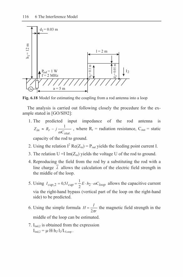
116 6 The Interference Model
Fig. 6.18 Model for estimating the coupling from a rod antenna into a loop
The analysis is carried out following closely the procedure for the ex-ample stated in [GO/SI92]:
1. The predicted input impedance of the rod antenna is
.
1
statrin C
jRZω
−≈ , where Rr = radiation resistance, Cstat = static
capacity of the rod to ground.
2. Using the relation I2 Re(Zin) = Prad yields the feeding point current I.
3. The relation U =I Im(Zin) yields the voltage U of the rod to ground.
4. Reproducing the field from the rod by a substituting the rod with a line charge λ allows the calculation of the electric field strength in the middle of the loop.
5. Using loopcapcap ChEII ω⋅⋅== 22, 215,0 allows the capacitive current
via the right-hand bypass (vertical part of the loop on the right-hand side) to be predicted.
6. Using the simple formula .2 r
IHπ
= the magnetic field strength in the
middle of the loop can be estimated.
7. Iind,2 is obtained from the expression Iind,2 = µ⋅H⋅h2⋅l2/LLoop .

6.4 Electromagnetic coupling 117
Evaluation:
1. Evaluating Eqs. (6.29) and (6.30) using the data in this example leads to an input impedance Zin = 2.53 - j 733 Ω.
2. I2 Re (Zin) = Prad yields the feeding point current I = 0.63 A.
3. From the current a voltage U to ground of U = 462 V is calculated.
4. An unknown finite line charge is placed on the axis of the rod. Its magnitude is chosen in such a way that, on the surface of the rod (at a height of 6 m), a voltage to ground of 462 V is obtained. To achie-ve this voltage, Eq. (6.31) is evaluated. Evaluation of the expression
leads to a related line charge of V7.374
≈=πελλ .
5. The related line charge λ of 37.7 V produces, according to Eq. (6.33) with z2 = h = 12 m, at a distance of 6 m, an electric field strength of E(6 m) = 7.0 V/m on the ground. The static capacitance of the horizontal part of the influenced loop amounts to 30 pF (ar-rangement 14 of annex A10). The capacitive current through the right-hand side bypass is
=⋅⋅⋅⋅⋅⋅⋅⋅== − AII capcap126
2, 103010221,06,65,05,0 π 124 μA.
6. The magnetic field strength in the middle of the loop can be calcu-lated as 16.7 mA/m.
7. Using a self inductance of Lloop = 1,48 μH for the loop (arrangement 11 of annex A10), the inductive current thought the right-hand by-pass amounts to
.83.21048.1/21.0107.16104.0 6362, mAAIind =⋅⋅⋅⋅⋅⋅⋅= −−−π .
The example in Fig. 6.18 has also been analysed using the program CONCEPT. In Table 6.1 the values of the computer simulation are com-pared with the approximations above. It should be noted that CONCEPT only displays a total value for the bypass current.
It can be seen that the values for the total current in the bypass and for the magnetic field disagree. This is not surprising as the approximation of the magnetic field strength assumes a constant current in an infinitely long vertical conductor. For a 24 m long conductor with a current linearly de-creasing towards its ends and a field point at a distance of 6 m this seems to be a very crude line charge replacement. However, the estimation deliv-ers higher values, which provides a degree of safety threshold.

118 6 The Interference Model
Table 6.1 Comparison of the results from a computer simulation with values gained by approximations (* values without the loop)
CONCEPT Approximations Input impedance 2.43-j610 2.53-j733 Ω Feeding point current 0.64 0.63 A Voltage of the antenna 391 462 V Total current through the bypass 1.61 2.83 mA Electric field strength in 6 m distance
6.0* 7.0 V/m
Magnetic field strength in 6 m distance
10.7* 16.7 mA/m
Example 6.8: Coupling of two loops - The input impedance of a loop an-tenna in the very low frequency range (where the radius Rloop of the loop is smaller than the wavelength λ) can be approximated by
selfradin LjRZ ω+≈ ,
Rrad = radiation resistance of the loop = 2
44320 ,Fπ
λ⋅ ⋅ Ω
Lself = self inductance of the loop = ⎟⎟⎠
⎞⎜⎜⎝
⎛−
⋅⋅⋅ 07.1)ln(0
wire
looploop R
RR
πμ ,
2loopRF ⋅= π .
The coupling of 2 circular loop antennas (loop radius Rloop = 0.5 m, wire radius Rwire = 1 mm) located at a distance of 1 km from each other has to be investigated at f = 10 MHz. From the source antenna a power of Pout = 1 W is radiated.
In Table 6.2 the following quantities are compared, as obtained from an approximation and from a computational simulation using CONCEPT: Zin, Isource, Usource, E1000, U2,open circuit .

6.4 Electromagnetic coupling 119
Table 6.2 Comparison of the results obtained by approximations with those ob-tained using a computer simulation
Approximations CONCEPT Input impedance 0.024 + j 248 0.027 + j 264 Ω Feeding point current 6.07 6.49 A Feeding point voltage 1.51 1.60 kV Electric field strength on the place of the victim loop with no loop ar-ranged
6.7 6.6 mV/m
Open circuit voltage of the victim antenna
1.1 0.71 mV
Remarks: According to table 5.1 a loop antenna has a directivity of 1.5. The loop has been replaced by an octagon in the CONCEPT-simulation.
7 Intrasystem Measures
EMC-intrasystem measures is a generic term encompassing all measures that can be taken in a system, in order to form a compatible system from a number of devices with well known (and also unknown) EMC-features.
The civilian standardisation is more-or-less a device-standardisation; it defines requirements for single devices or units. The linking of several de-vices to fulfil a common task, such as in an installation or system, is only treated using basic approaches.
Devices are tested to meet the limit values in specified test arrangements under well defined conditions. Reproducibility is of great importance in testing. However, when in use, the overall system may be completely dif-ferent. The power supply impedance does not necessarily match the course of the standard, and moreover, the impedance is variant in time, the lengths of the test cables are different to the lengths of the system cables and the system surrounding may lead to a capacitive loading and possibly to com-pletely different EMC-behaviour of the devices.
Well defined rules need to be taken with regards to the complete system. These intrasystem measures should be written as guidelines for the design engineers. They comprise:
• Grounding • Shielding • Cabling • Filtering
The military standardisation, which also specifies good practice in sys-tem installation, specifies both the device requirements and also require-ments for their assembly within the complete system. At this point, it is necessary to refer to the German standards, in which each intrasystem measure is discussed in a number of corresponding parts. The procedural standards are given by:
• VG 95 374 part 2: Program for Systems • VG 95 374 part 4: Procedures for Systems
The standard VG 95 374 part 2 describes what steps to do whilst plan-ning an EMC-system and the standard VG 95 374 part 4 specifies how to execute each step. K.-H. Gonschorek, R. Vick, Electromagnetic Compatibility for Device Design and System Integration, DOI 10.1007/978-3-642-03290-5_7, © Springer-Verlag Berlin Heidelberg 2009

122 7 Intrasystem Measures
Remark: The term intersystem measures summarises all measures nec-essary to ensure the EMC with the outer-world (the electromagnetic envi-ronment).
Grounding: The connection of a housing, reference conductor or pas-sive metallic superstructure parts to the (reference) ground.
According to VDE 847 T2, the reference ground of an electric appliance comprises the totality of all metal parts connected among each other, in an electric conductive way, to form an electrical balance for the considered frequency range and thereby establishing a reference potential. The refer-ence ground must not, in any case, be confused with the protection earth. The protective earth has the sole task of providing electric shock protection for the user of the system. In the sense of EMC a plane grounding system should be employed wherever possible.
Shielding: The electromagnetic decoupling of two spatial areas to eliminate or reduce the unwanted coupling between two areas with differ-ent electromagnetic surroundings.
The shielding in the sense of electromagnetic compatibility consists, in general, of metallic barriers. The efficiency and quality of the shielding depends on, among others things: the type of the field to be reduced, the material, and the shield construction, the shield integrity, leakages and the frequency of interest.
Cabling: A system of metallic conductors for the guided propagation of electric energy and electric signals.
The cabling measures, in the sense of EMC, comprise the treatment of the cable shields and their fixing points to the device. They include a treatment of the propagation of wanted signals, the elimination or reduc-tion of unwanted emissions into the surrounding (outer world) and also of couplings into the signal circuits from the environment. The outer conduc-tor of coaxial cables forms both the signal return path and the cable shield. Cable shields have to be, with no exception, connected to ground at both ends. Video, loudspeaker, microphone and sonar signals, propagated through coaxial cables, need a special treatment with respect to EMC.
Filtering: Measure for the decoupling of conducted signals of two dif-ferent spatial areas.
Filtering, in the sense of EMC, comprises all measures for the reduction of conducted signals. These measures include the electrical and mechani-cal construction of the filter elements, the filter house grounding and the resistive loading of the wires. EMC filters are constructed of LC-combinations, except in special cases. Filter circuits normally function in both directions.

7.1 Some remarks regarding grounding, shielding, cabling, and filtering 123
It is important to understand that filter circuits are reactive devices and do normally not convert electric power into heat. They are intended to act as an ideal short or open circuit for only the undesired frequency compo-nents, hence, they form a perfect mismatch for these frequencies. The sig-nal attenuation of a filter device is described by the insertion loss. For real-ised filter circuits the insertion loss should be as high as possible for the interference signal and very low for the desired signal.
The statements regarding grounding and filtering in this chapter are only a summary of the most important rules. Detailed explanations may be found in [GO/SI92].
EMC- Design guidelines: In the framework of the EMC-planning for a complex system (contain-
ing radio devices), the tailor-made intrasystem measures for the system should be compiled within an EMC-design guide. A possible structure of an EMC-design guide is presented in annex A7, which may be used as the basis of a system specific guide.
7.1 Some remarks regarding grounding, shielding, cabling, and filtering
7.1.1 Grounding
According to VG 95 375 part 6, the ground is formed by the entirety of all metal parts of the complete system, the installation and any devices that are connected using electrical conductors; which provide a reference po-tential (ground potential).
Fundamental statement
• Electrical/electronical devices must be grounded to a metallic device support in the following manner:
dimensions < λ/10 ⇒ grounding only at one point, dimensions > λ/10 ⇒ several grounding connections (depending on
the construction and the kind of the device).
• In addition, metallic parts of non-electric appliances should be in-cluded into the grounding system. In doing so the following properties are attained:

124 7 Intrasystem Measures
- approximation of an plane-shaped grounding system, - reduction of the radiation effect of passive radiators, - decrease of potential differences, - avoidance of HF-corona.
• Within power supply circuits, it is not necessary to ground conductors carrying operating currents for EMC reasons. If there is a requirement for grounding within alternating and three-phase systems, for some special reason, then the grounding can only be performed at one point.
• For frequencies f < 100 kHz and a symmetrical signal transmission, only the symmetry points are allowed to be grounded. For an unsym-metrical signal transmission, the reference conductor must be grounded at only one point.
• For frequencies f ≥ 100 kHz and impulse transmissions (digital sig-nals), a star-shaped reference conductor system is no longer adequate. A reference plane should be used, in its place.
• When grounding larger devices via ground strips, the ground strips should have a length L to width B ratio smaller than 5 (L/B ≤ 5).
• A valuable approach in assessing the quality of a ground connection is a measurement of the DC-resistance RDC. A value of RDC < 10 mΩ be-tween device and ground will meet the requirements. This value should be included within system specifications (a proof is also possible at 50 Hz).
• The protection earth (yellow-green) is by no means a HF-ground. The use of the protection earth as a HF-ground should only be considered as a compromise.
7.1.2 Shielding
Shielding comprises all measures taken to reduce the electric, magnetic and electromagnetic field in a volume bounded by the shielding measure.

7.1 Some remarks regarding grounding, shielding, cabling, and filtering 125
Shieldingchapter 7.2 - 7.6
t/d < 0.001chapter 7.2
High frequency fields(plane wave, plane shielding area)
Medium frequencymagnetic fields
Low frequency magnetic fields,magnetic DC-fields
d = 1
π μκf
t = thickness of the material
Theory of Schelkunoff,chapter 7.4
High impedancefieldschapter 7.4.1
Low impedancefieldschapter 7.4.2
Le o (chapter 7.5)
* Mesh shielding (HF)* Glances, holes
* Low frequency resonances* Cavity resonances
akages, penings, Cavity resonances
chapter 7.5.1
chapter 7.5.2
chapter 7.6Cables shielding
Electricfields
t/d < 0.001chapter 7.3.1
0.001 < t/d < 1chapter 7.3.2
0.001 < t/d < 1000
Fig. 7.1 Flowchart for selecting the problem-matched shielding
Fundamental statements
• Electric fields can be easily shielded (chapter 7.2). The shielding can be obtained using thin conductive foils. However, leakages (field pene-trations) have to be avoided.
• Magnetic fields are difficult to shield (chapter 7.3). Thick-walled high-permeable shielding boxes are necessary to shield static magnetic fields. The smaller the volume, the higher the shielding effect. Thick-walled shielding boxes of high conductivity are required for shielding low frequency magnetic fields. The larger the volume to be shielded, the higher the shielding effect.
• The material used when shielding high-frequency fields is not the sig-nificant property (chapter 7.4). The material in very thin shielding lay-ers, such as metallisation on synthetic materials or glasses, only plays an important role in terms of its environmental and structural behaviour (corrosion). Leakages (chapter 7.5) affect the fundamental properties of the shield and must be avoided.

126 7 Intrasystem Measures
• The quality of cable screens is described by the cable transfer imped-ance (chapter 7.6), the smaller the cable transfer impedance the better the shielding effect of the screen.
The diagram shown in Fig. 7.1 provides a flowchart for the selection of the problem-matched shielding solution.
7.1.3 Cabling
Cables and transmission lines interact with the electromagnetic environ-ment. Electromagnetic fields are produced around the cables, and in the region nearby, due to the transmitted power and signals. The generated fields are only zero in the ideal case of a completely symmetrical coaxial cable with a solid shield. On the other hand, cables also absorb signals from the environment and lead them to the device inputs.
General statements for an EMC-acceptable system cabling are described in depth in [GO/SI92]. Therefore, it is not necessary to repeat all aspects in this text. Nevertheless, some aspects are described in detail here as aid to understanding.
System cabling
It is helpful to group all of the cables within a system into categories in terms of the signals they are carrying. All cables of a certain category have the same, or at least similar, EMC-features. They are either very sensitive, sensitive, perturbing, strongly perturbing or indifferent; with consideration to the connected circuits in each case. There are no special coupling risks if cables of the same cable category are placed very near to each other (on the same cable tray). In addition, the systems become more easily under-standable through cable categorisation.
An example, in the style of VG 95 375 part 3, for the definition of cable categories is shown in Fig. 7.2. The required separation distance between cables of different categories are specified in Fig. 7.3, the results are shown with respect to the example of Fig. 7.2.

7.1 Some remarks regarding grounding, shielding, cabling, and filtering 127
cablecategory
example forcable type
wanted signal noise effect typical application
1insensitive,disturbing
2insensitive,not disturbing
3sensitive,not disturbing
4verysensitive,not disturbing
5insensitive,not disturbing
special cablesPlease look to the remark!
12 to 1000 VDC, 50, 60, 400 Hz,narrow band
10 bis 1000 V,RF, HF,narrow band
bis 115 V,RF,narrow band
up to 15 V:MF,broad band,up to 115 V: LF~0,1 V bis 500 mV,DC, RF, HF,narrow band
μ
narrow band,broad band
narrow band,broad band
narrow band,broad band
narrow band
broad band
power supply cables,normal control cables,cables for lighting systems,cables for alarm systemstelecommunication cables,control and signal cables,,cables for synchro-connections,carrier frequency cables
cables for small signals,synchronising and impulse cables
antenna cables for reception,telecommunication and informationcables, cables for radar warning reception
transmit/receive cables,converter cables (not filtered), cables for ignition circuits, microphone cablesl
Cables for special applications,antenna cables for transmission
twisted,shielded,twisted andshielded
shieldedor coaxial
shieldedor coaxial
coaxial
twisted
Fig. 7.2 Example for the definition of cable categories in the style of VG 95 375
part 3
Remark: A single analysis has to be carried out for every special cable (sonar, transmit/receive) and its placement has to be specified.
In every complex system the cables should be divided into cable catego-ries. Whether 5 categories are necessary may be questionable. In most cases 3 categories (sensitive, indifferent, perturbing) are sufficient. Whether the specified separation distances (Fig. 7.3) are necessary, or whether a larger distance should be chosen, must be the responsibility of the EMC system designer. Experiences within military shipbuilding have shown that the classification into cable categories according to Fig. 7.2, together with the separation distances according to Fig. 7.3, provide a good compromise between cost and lowering the EMC-risk.
The table of cable categories with their separation distances is an essen-tial part of the EMC-design guidelines. The table has to be made available to the device designer and builder. He should be able to state the category of all cables leaving or entering his device.

128 7 Intrasystem Measures
1 2 3 4 5
1
2
3
4
5
0.1
0.1 0.1 0.1 0.1
0.1
0.1 0.1 0.1
0.1
0.1 0.1 0.1
0.1
0.1
0.1
0.2
0.2
0.20.2
Category
Fig. 7.3 Separation distances in metres for the parallel laying of cables of differ-
ent categories
The subject of ‘cable coupling’ is inexhaustible and will occupy EMC-engineers for a considerable time to come. Fig. 7.4 shows a flowchart for navigating through the different aspects of cable coupling in this book. It is hoped that it will also provide systematic understanding for the cable cou-pling to aid the reader.
System cabling Two wire cablesuntwisted,twisted
Emission Coupling-in Influence of shield connection
Coaxial cables
chapter 7.6.4
Emision andcoupling-inchapter 7.6.3chapter 6.3 and 7.6.2chapter 4.4
chapter 7.1
Cable couplingchapter 7.6 and A9models: chapter 7.6.1
Fig. 7.4 Flowchart for cable coupling
Some questions of cable coupling remain open, for instance: • transmission line currents and antenna currents on slightly unsym-
metrical lines above ground, • symmetrical and asymmetrical attenuation, • treatment of twisted cables in the HF-region, • optimisation of cable screens, • connection of cables to large stray bodies within numerical field
simulations.

7.1 Some remarks regarding grounding, shielding, cabling, and filtering 129
7.1.4 Filtering
Filtering, in the sense of EMC, comprises all measures that reduce con-ducted signals. This includes the electrical and mechanical construction of the filter elements, the grounding of the filter box and the resistive loading of the wires. Additionally, filtering comprises the fulfilment of limit values for lines and most importantly for power supply lines. Filter circuits also have the task of ensuring that the shielding efficiency of cabins, housings and boxes is not jeopardised.
A typical filtering situation is as follows: A very strong radio signal is coupling into a power supply line. The
power supply line is transporting the signal conductively into the shielded area. Hence, the radio signal arises within the shielded room through irra-diation from the line.
In order to eliminate this path of unwanted signal propagation, all wires that penetrate into the shielded area must be filtered; except in a few spe-cial cases. The frequency range of the wanted signals must be considered when implementing filter circuits.
For standard applications (power supply lines, telephone lines, low fre-quency signal lines) pre-manufactured filters are available on the market.
In special cases, filter circuits may have to specifically designed. There-fore, to provide an understanding of this subject, the analysis of a filter cir-cuit with Butterworth-characteristic is presented here.
Butterworth filter with low-pass characteristic
A Butterworth-filter is characterized by the fact that the pass band is maximally flat and no ripples occur. However, in return, the filter ap-proaches the stop band with a gentler slope than other filters.
The transfer function of the Butterworth-low pass filter (ω = k⋅ωgo), normalized to ω = ωgo = 1is given by:
( ) ,...
1)()(
22101
2 KsasasaasU
sUNn
n
⋅⋅+⋅+⋅+
==ω (7.1)
.ωjs= , where n represents the order of the low pass filter.
The coefficients ai are given in Tab. 7.1.

130 7 Intrasystem Measures
Tab. 7.1 Coefficients for the defining of a Butterworth low-pass filter, dimen-sion of the coefficients: dim(ax) = secondsx
n a0 a1 a2 a3 a4 a5 a6 1 1 1 2 1 2 1 3 1 2 2 1 4 1 2.613 3.414 2.613 1 5 1 3.236 5.236 5.236 3.236 1 6 1 3.864 7.464 9.141 7.464 3.864 1
From the transfer function the normalized amplitude of the filter is given by
( )2
0
1
1n
g
N Kωω
ω
= ⋅⎛ ⎞
+ ⎜ ⎟⎜ ⎟⎝ ⎠
. (7.2)
From Eq. (7.2), the order of the filter required to obtain a particular steepness can be predicted. K is a normalizing factor, which has been cho-sen to be 1 in subsequent evaluations.
Example 7.1: Predicting the necessary order n of a Butterworth-filter, if the output voltage at goωω 2= has to be lower than 1 % of the input voltage ( inout UU ⋅≤ 01,0 ).
Using Eq. (7.2) and choosing K = 1 yields
( ) .21
11022
2
ngoN+
≥≤= −ωω (7.3)
From this equation it follows
.7
,64.62log
2,42log2
,102,1021 4242
=
=≥≥⋅
≥≥+
n
nn
nn
(7.4)
Using a Butterworth-low pass filter of the order n = 7 leads to an ampli-tude-frequency characteristic whereby, at the double value of the critical angular frequency ωg0, the amplitude is smaller than 1 % of the driving voltage.
The amplitude-frequency characteristics of the Butterworth-low pass fil-ter of the orders 1 to 4 are shown in Fig. 7.5. A characteristic frequency in

7.1 Some remarks regarding grounding, shielding, cabling, and filtering 131
the amplitude-frequency plot is the cut-off frequency or the critical fre-quency (angular frequency) ωg0. At this frequency the amplitude has re-duced from a value of 1 to the value 2/1 .
0.707n = 1
n = 2
n = 3
1
2 g0g0
|N( )|
Fig. 7.5 Amplitude-frequency characteristic of the Butterworth transfer function,
K = 1
Procedure for defining a filter:
1. Prediction of the necessary amplitude characteristic and hence the order of the filter.
2. Selection of the circuit: Normally, every additional independent reac-tive element leads to an increment of 1 in the order of the filter.
3. Calculation of the normalised circuit elements (R0i, C0i, L0i).
4. Conversion of these circuit values, which are related to ωg0, to the ac-tual critical angular frequency ωg.
For the frequency conversion the following relations apply:
,0ii RR = (7.5)
., 00B
LL
BC
C ii
ii == (7.6)

132 7 Intrasystem Measures
The index 0 represents the values of the normalized low pass filter.
0g
gBωω
= is the ratio between the actual critical frequency and the normalis-
ing critical frequency.
LP 0L (7.7)
HP g0 0
1Lω ⋅ω⋅
(7.8)
g0 0Lω ⋅
ω (7.9)
BP
2g0 m 0L
ωω ⋅ω ⋅
(7.10)
LP 0C (7.11)
HP g0 0
1Cω ⋅ω⋅
(7.12)
g0 0Cω ⋅
ω (7.13)
BP
2g0 m 0C
ωω ⋅ω ⋅ (7.14)
2m g1 g2'ω = ω ⋅ω (7.15)
g2 g1'ω = ω − ω (7.16)
Fig. 7.6 Converting a low pass (LP) to a high pass (HP) and a band pass (BP) fil-ter
The table has to be read in the following way:
Firstly, a normalized low pass filter (LPF) with the desired steepness has to be developed. If it is now required, for instance, to produce a high pass filter (HPF) with the actual critical angular frequency ωg , all inductances (Eq. (7.7)) have to be replaced by capacitances according to Eq. (7.8) and

7.1 Some remarks regarding grounding, shielding, cabling, and filtering 133
all capacitances (7.11) by inductances according to Eq. (7.12). All induct-ances change to series and all capacitances to parallel resonance circuits when dimensioning a band pass filter.
Insertion loss
The insertion loss is the attenuation of a high-frequency harmonic voltage when a suppression element, or circuit, is inserted between the interference source (HF-generator) and the interference victim (load). Where the source has the defined output impedance Z0 (Ζ0 commonly 50 Ω) and the load has the impedance Ζ0, (see Fig. 7.7).
The insertion loss is given by
[ ]dBUUa
aE 2
log20 010⋅= (7.17)
U0 = open circuit voltage of the source, Ua = voltage across the interference victim.
U0
Z0
Z0
Ua
suppression
element
interference source interference victim Fig. 7.7 Suppression element between interference source and victim
The insertion loss can only serve to provide a comparison of differ-ent filter circuits because, normally, it does not give direct informa-tion about the effect in a real arrangement (with unknown imped-ances).
The fundamental arrangement of a low pass filter is presented in Fig. 7.8 (taken from [GO/SI92]). It is important to note, that if there is a low im-pedance interference source (thyristor) the filter should start with an induc-tance in order to raise the internal impedance of the interference source.

134 7 Intrasystem Measures
G ZL
0 0
0
0
no
no
yes
yes
0
0
0
0
plain filter better filterrisk of a signal amplification
Z
Fig. 7.8 Fundamental arrangements of low-pass filters
Example 7.2: Developing a Butterworth-low pass filter of the order 3 a) The reactance values are predicted for the low pass filter shown in
Fig. 7.8 in such a way to get a normalised Butterworth low-pass filter of the order 3.
b) The low pass filter has to be transformed into a high pass filter, and then,
c) into a band-pass filter with a bandwidth of Δω. d) The real elements of the low-pass filter have to be predicted for
R1 = R2 = 50 Ω and a critical frequency of f0 = 100 kHz.

7.1 Some remarks regarding grounding, shielding, cabling, and filtering 135
R2C1
L
C2
R1
U1 U2
R = R = 11 2
Fig. 7.9 Circuit for producing a Butterworth low-pass filter of the order 3
a) Based on the assumption R1 = R2 = R, the transfer function can be de-rived to be
2
0101 02
3 20 01 02 0 01 02
1 1( ) .2
( ) 12 2 2
UN LU RC RCL RC C L C C Rs s s
ω = = ⋅+ ++
+ + +(7.18)
According to Tab. 7.1 the following three equations can be derived (with units shown in square brackets):
202010 =CRCL [s]3 , (7.19)
4)( 02010 =+ CCL [s]2 , (7.20)
4)( 00201 =−+
RL
CCR [s]. (7.21)
Solving these 3 equations for the three unknowns leads to
0 01 022 , 1L H C C F= = = . (7.22)
b) The conversion of a low-pass filter into a high-pass filter is carried out via the transformation equations:
00
1
iggi C
L⋅⋅
=ωω
, (7.23)

136 7 Intrasystem Measures
00
1
iggi L
C⋅⋅
=ωω
, (7.24)
with gω = actual critical angular frequency and 0gω = normalised critical angular frequency.
c) The conversion of a low-pass filter into a band-pass filter is performed via the following transformation equations.
An inductance transforms into a series resonant circuit with:
imgi L
C0
20 ⋅⋅
=ωωωΔ , (7.25)
ωΔω 00 ig
i
LL
⋅= . (7.26)
A capacitance transforms into a parallel resonant circuit with:
02
0 imgi C
L⋅⋅
=ωωωΔ , (7.27)
ωΔω 00 ig
i
CC
⋅= , (7.28)
where 1 2m g gω ω ω= , 1 2g gω ω ωΔ = − , 1 2,g gω ω = upper and lower
critical angular frequency. d) Substituting the resistances R1 and R2 of 50 Ω into part a) leads to the
new values for L0 and C0i: L0 = 100 H, C01 = C02 = 20 mF.
Using the frequency conversion relations of Eq. (7.6) yields the actual values: L = 159 μH, C1 = C2 = 31.8 nF. The amplitude-frequency characteristic of the low-pass filter is presented in Fig. 7.10.

7.1 Some remarks regarding grounding, shielding, cabling, and filtering 137
0 1 2 3 4
0.1
0.2
0.3
0.4
0.5
f
fg
U
U
2
1
Fig. 7.10 Amplitude-frequency characteristic of the treated Butterworth low-pass
of the order 3
At the critical frequency the amplitude ratio amounts to
( )010.707 0.3535 ,2gN ω = ⋅ = (7.29)
for a frequency ω = 2ω0, it can be calculated to be
( )0 6
1 12 0.06221 2
gN ω = ⋅ =+
. (7.30)
The three derived circuits are shown in Fig. 7.11.

138 7 Intrasystem Measures
R
R
LS
CS
CS
CS
R
RL L
LP
LP
C
R
R
L
C C
high pass
low pass
band pass
Fig. 7.11 Conversion of a low-pass filter into a high-pass and band-pass filter
Exercise
Exercise 7.1: A power line filter (low-pass filter), for a thyristor control unit, has to be developed. The following requirements are given: 1. The filter circuit should have a critical frequency of 200 Hz. 2. The filter should show an attenuation (|N(ω)|) of 60 dB at 10 kHz.
a) What order should the Butterworth-low pass filter have? b) Present a proposal for a filter construction and justify the arrangement
of the filter elements.
7.2 Shielding against electric fields - shield of bars
Electric fields can be easily shielded. Electric field lines start and end on charges. Therefore, it has to be guaranteed that the charges can arrange in such a way that the shielding effect may occur. This principle is demon-

7.2 Shielding against electric fields - shield of bars 139
strated with the following example. Two plates inside an electrostatic field are shown in Fig. 7.12. What is the charge distribution that will be formed?
a) b)
Fig. 7.12 Shielding of electric fields by 2 plates, a) without connection, b) with
connection
In the left drawing, the field is almost unaffected by the presence of the plates. However, in the right drawing, the charges are able to counterbal-ance. No field can exist between the two plates any longer (at least theo-retically).
z
yh
2sx E0
→
2 R
R << hR << s
Fig. 7.13 Shielding of electric fields by wire bars (chicken wire shielding)
In many cases the installation of plates can prove to be expensive. Therefore, shields constructed of bars for shielding electric fields should be taken into consideration. In Fig. 7.13 such a shield construction made with bars is shown (mesh shield).
This mesh shield has an attenuation [SIN69] against electric fields of

140 7 Intrasystem Measures
Rhh
saS
π
π
2ln
2log20⋅
⋅= . (7.31)
The value given by Eq. (7.31) is valid for the centre point of the space shielded by the bars.
A shield of bars (shielding a chamber) with the following parameters: Height of the room: 2s = 2 m, Radius of the wire bars: R = 2 mm, Mesh size h = 10 cm has a shielding efficiency of 29.6 dB according to the Eq. (7.31).
To allow the charges to counterbalance on the bars, additionally the fol-lowing conditions must be met:
• All intersections of the bars should be connected conductively (welded).
• An electrical connection between the top and bottom bar arrange-ments is essential.
Exercises
Exercise 7.2: A shielding efficiency of aS = 40 dB against electrostatic fields is required in a cinema hall. The cinema has a height of 2s = 10 m.
a) How large is the width in the wire mesh (h in Fig. 7.13) necessary, if the radius of the bars (wires) amounts to R = 2 mm?
b) It is intended to use the steel reinforcement of the ceiling and the floor of the cinema for the shield purposes. The rod radius of the steel mesh amounts to R = 5 mm and the mesh width is h = 20 cm. How large is the shielding efficiency in this case?
c) A medium wave radio station (f = 1 MHz) is located near to the cin-ema (distance d = 200 m). It produces a vertical electromagnetic field of 10 V/m at the location of the cinema. Do you think it is sufficient to use the relations of electric fields for evaluating the shielding effi-ciency, explain your decision. Are the real shielding values higher or lower than the values calculated with the relations for the electrostatic field?
Exercise 7.3: The shielding of a living room is realised by rods. In the ceiling (height of 2.7 m) and the floor a mesh of bars is installed (radius of the rods R = 3 mm, mesh width h = 5 cm). The room has a size of A = 15 m2. The floor and the ceiling mesh are connected by a single wire.

7.3 Shielding against magnetic fields 141
An overhead line (50 Hz) exists near to the shielded room, which produces an electric field strength of 10 V/m at the position of the room.
a) What is the field strength in the middle of the room? b) What current can be measured in the connection wire between the
ceiling and the floor mesh? c) Do you think it is necessary to ground the ceiling and/or the floor
mesh? What are the advantages if the meshes are grounded?
7.3 Shielding against magnetic fields
Magnetic fields are difficult to shield, especially low frequency or static magnetic fields.
The positions of devices and sensors have to be defined in the planning phase of a system. The positions should be defined so that the effect of low frequency magnetic fields (monitors, microphones, electron beam mi-croscopes, video devices) is reduced. This involves taking the distance be-tween the interference source and victim into consideration.
The shielding against magnetic fields may be divided into shielding against the following:
a) static and very low frequency fields – shielding by redirecting the field (chapter 7.3.1),
b) medium frequency fields – shielding by inducted currents and use of the skin effect (chapter 7.3.2),
c) high frequency fields – shielding by reflections and absorption (the-ory of Schelkunoff, (chapter 7.4).
7.3.1 Shielding against static magnetic and very low frequency magnetic fields
In the shielding of very low frequency fields (DC, fields from railway cur-rents of 16 2/3 Hz and fields from normal power supplies) the concept is exploited that magnetic fields will be guided by magnetic materials. The magnetic field is directed around the area to be protected. Immediately, it is clear that for shielding the following rules are valid:
• the higher the permeability of the material the higher the shielding efficiency,
• the thicker the material the higher the shielding efficiency,

142 7 Intrasystem Measures
• the smaller the volume to be protected the higher the shielding effi-ciency.
For a cylinder of material with a relative permeability of μr , an inside radius of R and a thickness of t, the following elementary equation can be derived:
⎟⎠⎞
⎜⎝⎛ ⋅
+⋅=⎟⎟⎠
⎞⎜⎜⎝
⎛⋅=
Rt
HHa r
i
aS 2
1log20log20 μ . (7.32)
In most cases the approximation
⎟⎠⎞
⎜⎝⎛ ⋅
⋅=R
ta rS 2
log20 μ (7.33)
yields sufficiently precise results. The front view of a hollow cylinder containing a monitor housing is
shown in Fig. 7.14. As a ‘worst-case’ approximation the diameter 2R of the shielding cylinder should be chosen to be the diagonal measurement of the rectangular monitor housing (The larger the shielding structure, the smaller the shielding efficiency).
R
t
t
BB
Fig. 7.14 Front view of a cylinder containing a monitor housing within a magnetic
field perpendicular to the longitudinal axes
Eq. (7.32) and subsequently Eq. (7.33) have been derived for a magnetic field perpendicular to the axis of a very long cylinder.

7.3 Shielding against magnetic fields 143
Service and inspection openings within magnetic shields
Access openings are necessary within practical shielding boxes (to view the monitor screen, for example). The question often arises as to what ex-tent approximations are possible for such a situation. An estimate of the in-fluence of an opening is shown in Fig. 7.15. The shielding efficiencies were calculated by the company Vakuumschmelze [VAC80] and are re-peated here. The attenuation due to the material is assumed to be much higher than the measured values. The shielding factor is presented, which can be converted into a dB-attenuation using aS = 20 log S. If both the in-fluence of the material and the influence of the opening has to be consid-ered then a linear superposition must be performed.
13
51
35
13
5
2
0.2 0.5 1.0 1.5
5
10
20
50
100
200
500
x/Di
xD
i
sta
tic,acro
ss
sh
ield
in
gfacto
rS
50H
z,ac
ross
1000
Hz,
acro
ss
220
Hz,
acro
ss
0-1
0kH
z,le
ngth
wis
e
Fig. 7.15 Influence of an opening within a cylinder
Example 7.3: The shielding efficiency of a monitor housing (17 inches screen diagonal) made of mu-metal (µr = 20 000) with a thickness of 2 mm has to be predicted. The field to be shielded is the magnetic field perpen-dicular to the beam axis. The two configurations of interest are a box

144 7 Intrasystem Measures
closed at all sides (case a) and a box completely open on the front side. The shielding efficiency is calculated for a field point 10 cm behind the front plane (case b).
a) Using Eq. (7.33) yields aS = 39 dB. b) From the diagram in Fig. 7.15 where x/D = 0.23, a value of S = 15
can be obtained, which leads to a shielding efficiency of aSM = 23.5 dB. The attenuation due to the material is almost 16 dB higher, however, so it can be neglected in this case. If the attenuation due to the material has a similar value to the opening’s influence, an approximation of the total shielding efficiency can be carried out us-ing the following formula:
⎟⎟⎠
⎞⎜⎜⎝
⎛+⋅−=
−−2020 1010log20SMaSa
Sga . (7.34)
Substituting the values of this example into Eq. (7.34) yields
.2.221010log20 2039
205.23
dBaSg =⎟⎟⎟
⎠
⎞
⎜⎜⎜
⎝
⎛+⋅−=
−− (7.35)
Double-walled shields
A number of shielding questions regarding magnetic field shielding meas-ures are treated in the application notes of the manufacturer Va-kuumschmelze [VAC88], which it is recommended the reader consults. The following formula for double-walled shields is presented:
⎟⎟⎠
⎞⎜⎜⎝
⎛ ⋅⋅⋅⋅=
221
2log20R
SSaS
Δ , (7.36)
R2 is the inner radius of the outer cylinder, S1, S2 are the shielding factors of the single shields and Δ is the air gap between both single shields.
In deriving this formula it is assumed that the air gap Δ is significantly smaller than the inner radius R2 of the outer cylinder.
Example 7.4: The shielding efficiency of a double-walled shielding box (constructed of cylinders) has to be compared with that of a single-walled shield of a corresponding thickness,
• Parameters for the double-walled box: µr = 25 000, t = 1 mm, R1 = 25 cm, R2 = 30 cm,
7.3 Shielding against magnetic fields 145
• Parameters for the single-walled shield: µr = 25 000, t = 2 mm, R = 25 cm.
The following shielding factors can be calculated for the double-walled housing: S1 = 51, S2 = 43, and a total shielding efficiency of 57 dB. A shielding efficiency of 40 dB is calculated for the single-walled box.
Subsequently, the radius R2 has to be doubled, however, the air gap should stay at approximately 5 cm (R1 = R = 55 cm). These new assump-tions lead to the values
S1 = 23.7, S2 = 21.8, aS,double = 38.7 dB, aS,single = 33.3 dB.
It has to be considered that the housings become a little bit bigger; ap-proximately two times the air gap.
Compensation coils
Compensation coils are also used for the reduction of low frequency mag-netic fields. The compensation coils measure the three-dimensional field and produce a corresponding compensation field. Commercially available compensation equipment (right) and a commercially available box made of mu-metal (left) are shown in Fig. 7.16. The compensation coil shown com-pensates very well for 16 2/3 Hz and 50 Hz alternating magnetic fields, up to field strength values of 20 A/m. It only shows weaknesses in switching on and off in very high fields. Furthermore, it has been detected that the compensation is only satisfactory against fields from a single source.
In an environment with more than one low frequency magnetic interfer-ence source (in a factory building with several independently working welding sets) it is better to use a mu-metal shielding box. Alternatively, it may be better still to use a TFT-monitor.

146 7 Intrasystem Measures
Fig. 7.16 Mu-metal box and compensation coil with electronics for the reduction
of magnetic fields: a) Left: empty mu-metal box, right: compensation coils; electronics shown in
the centre b) Mu-metal box with monitor c) Compensation coils with monitor

7.3 Shielding against magnetic fields 147
Fig. 7.17 Measurement set-ups to measure the shielding efficiency
The arrangements used to measure the shielding efficiency of the mu-metal box (material thickness d = 1mm) and of the compensation coils are presented in Fig. 7.17.
Fig. 7.18 Measurement curves for the test set-ups according to Fig. 7.17
The measured field curves are shown in Fig. 7.18. The dependency of the field due to the current within the coil is shown, where the coils are used to produce the field within the laboratory. The investigations were carried out by a master’s student (Stephan Pfennig) within his project work.

148 7 Intrasystem Measures
Some guidance for defining a shielding housing
The formulas presented for shielding housings assume that permeability is constant and that no saturation effect occurs within very high fields. In re-ality, this is not completely true. From experiences regarding shielding boxes and the economical dimensioning of housings to protect against low frequency magnetic fields, the following statements are given as guidance:
1. For magnetic interference fields lower than 2 A/m a steel box µr = 200), covered with Vitrovac (amorphous high permeable mate-rial), should be sufficient.
2. For magnetic interference fields Htat from 2 A/m up to 40 A/m, a mu-metal box of thickness t where
[ ] [ ]/[ ]
1000
H A m Diagonal cmtatt mm⋅
= (7.37)
has proven to be the best solution.
3. For magnetic interference fields from 40 A/m up to 100 A/m a dou-ble-walled shielding housing with dimensions derived from Eq. (7.36) should be chosen.
4. For magnetic interference fields above 100 A/m, a box should be constructed with an outer shell made of magnetic steel.
5. For a more precise approximation when considering optimised mag-netic shields, the assumption can be made that the magnetic field up to a distance equal to the diameter (2R, two times the radius) has to be guided through the shielding material. This statement is illustrated in Fig. 7.19.
t
2R
R
B
BB t
2RB= amat
i
a
Fig. 7.19 Concentration of the magnetic flux density through the magnetic
conductor

7.3 Shielding against magnetic fields 149
7.3.2 Shielding against medium frequency magnetic fields
In order to shield magnetic DC fields the shielding effect is obtained through redirection of the field (chapter 7.3.1). Alternating magnetic fields induce induction voltages within metallic circuits and materials. If these voltages are short circuited, however, induction currents occur with a di-rection and phase to compensate the initial fields.
Looking at these reactions at the microscopic level reveals that skin ef-fect theory must be considered. Treating these reactions macroscopically leads to the compensation currents. The two effects are not clearly distin-guishable in every case. A basic knowledge of the skin effect is necessary in order to understand the eddy current attenuation in the sense of EMC. A very simple introduction is delivered in annex A6.1. On the other hand, it can be derived from the macroscopic treatment that the compensation cur-rent is required for a good shielding effect. Therefore, measures have to be taken to allow the compensation current to flow. Principally, the plates must be connected to each other by a short circuit frame in order to get a shielding effect. The complete shielding arrangement is shown in Fig. 7.20.
The following Eqs. (7.38) to (7.43) are taken as given. However, the method of obtaining them is always the same: An alternating magnetic field in a certain direction is assumed then, from Ampere’s law and the in-duction law, a differential equation for the magnetic field is produced and solved by fulfilling the boundary conditions
Htan1 = Htan2, Etan1 = Etan2
at the air/material and material/air transitions.
7.3.3 Two parallel plates shielding against alternating magnetic fields
tkhKtkhHH
a
i
⋅⋅+⋅=
sincos1 (7.38)
i
aS H
Ha log20 ⋅= (7.39)

150 7 Intrasystem Measures
2s
t
Ha Ha
I
I
ω π
κ
μ
ωμκ
= angular frepuency = 2 f
= conductivity
= permeability
k = j = (1+j)
K = k s
1d
μμ
0
Fig. 7.20 Two parallel plates shielding against alternating magnetic fields
7.3.4 Hollow sphere shielding against magnetic fields
tkhK
KtkhHH
a
i
⋅⋅⎟⎠⎞
⎜⎝⎛ ++⋅
=sin2
31cos
1 (7.40)
i
aS H
Ha log20 ⋅= (7.41)
R
t
Ha K = k R
0
Fig. 7.21 Hollow sphere within an alternating magnetic field
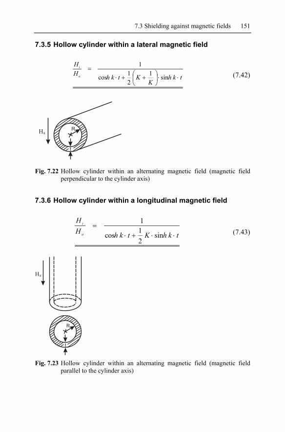
7.3 Shielding against magnetic fields 151
7.3.5 Hollow cylinder within a lateral magnetic field
tkhK
KtkhHH
a
i
⋅⋅⎟⎠⎞
⎜⎝⎛ ++⋅
=sin1
21cos
1 (7.42)
R
t
Ha
Fig. 7.22 Hollow cylinder within an alternating magnetic field (magnetic field
perpendicular to the cylinder axis)
7.3.6 Hollow cylinder within a longitudinal magnetic field
tkhKtkhHH
a
i
⋅⋅+⋅=
sin21cos
1 (7.43)
Fig. 7.23 Hollow cylinder within an alternating magnetic field (magnetic field
parallel to the cylinder axis)

152 7 Intrasystem Measures
Exercises
Exercise 7.4: Interferences (shaking display) were observed on the moni-tors inside an office near to a railroad track. The shaking display images occurred on the screens with a maximum deflection from their mean posi-tion of d = 3 mm. The monitor interferences occurred regularly each 5 to 10 minutes with a duration of approximately 10 s. No passing trains can be observed at the time of the interference.
a) Analyse the situation. b) State some counter measures and give an explanation for your
choices.
Exercise 7.5: A lateral magnetic field of 8 A/m is measured at the posi-tion of a monitor (50 cm diagonal). How thick must the walls of a mu-metal box (µr = 25 000) be if a field attenuation of 30 dB is required?
Exercise 7.6: What is the shielding efficiency obtained using a metal housing (thickness of the walls d = 2 mm) made from construction steel (κr = 0.17, µr = 200) at f = 50 Hz, where the inner dimensions are: length l = 60 cm, width b = 30 cm and height h = 30 cm?
a) Predict the shielding efficiency using the equations for parallel plates (distance between the plates 2s = b).
b) Predict the shielding efficiency using the equation for the hollow sphere (radius R = b/2!).
c) Predict the shielding efficiency using the equation for a hollow cylin-der within a lateral magnetic field (radius R = b/2).
Exercise 7.7: Prove that the Eq. (7.42) (hollow cylinder within an alternat-ing magnetic field, field perpendicular to the cylinder axis) reduces to Eq. (7.33) (hollow cylinder within a static field, perpendicular to the cylinder axis) at the frequency f = 0.
Exercise 7.8: a) The shielding efficiency against alternating magnetic fields has to be
calculated for a cubical shielding box (wall thickness d = 2 mm, di-agonal dimension D = 60 cm). What radius has to be chosen for the substituting sphere if a ‘worst-case’ estimation is desired. Give rea-sons for your answer.
b) What is the radius that has to be chosen for the substituting cylinder if the shielding is to be against a static magnetic field? Give reasons for the answer.
Exercise 7.9: An alternating magnetic field (50 Hz) of 2 A/m irradiates on a hollow cylinder at an angle of 30° in relation to the cylinder axis. The hollow cylinder has an inner radius of 10 cm, a wall thickness of 2 mm and

7.4 Shielding theory according to Schelkunoff – short and concise 153
is made from generator plates IV (κr = 0.032, µr = 600). How large is the magnetic field on the axis of the hollow cylinder?
Exercise 7.10: Five monitors (diagonal dimension 60 cm) are positioned within an office room having the size 5 m x 5 m x 2.5 m. The monitors suffer interference from a very strong static magnetic field due to a MSR-installation. Mu-metal housings with a wall thickness of 1 mm are pro-posed to eliminate the interferences. Shielding of the whole room is dis-cussed as an alternative. Why is the shielding of the whole room not a practical option when compared to shielding the individual monitors?
7.4 Shielding theory according to Schelkunoff – short and concise
The shielding theory of Schelkunoff is based on an impedance concept. The (plane) electromagnetic wave impinging on a shielding wall has a cer-tain wave impedance Γa, which is defined by the distance between the field source and the shielding wall. The shielding wall, by itself, has a wave im-pedance Γm, which depends only on the electric parameters and the fre-quency. In the interface between the air and metal wall, some reflections occur due to the mismatch between the differing impedances, Γa and Γm. A proportion of the wave penetrates into the material and is attenuated and phase shifted according to the skin effect theory. Another reflection occurs when the penetrating wave strikes the second interface, due again to the impedance mismatch. A proportion of the wave is reflected and a propor-tion of the wave comes out. For the re-reflected wave, the process repeats with attenuation, phase shifting, impinging on the interface, reflection and so on. The behaviour is presented schematically in Fig. A6.1.
If the impinging wave is defined by the electric field strength of 1 V/m, for instance, then the total field strength emerging out of the other side of the shielding wall can be calculated using Eq. (7.44). The transferred field tw V/m due to an incoming field strength of 1 V/m is given by
tma
tmaamw er
etttγ
γ221
1−
−
⋅−⋅⋅⋅= . (7.44)
Therefore, the shielding efficiency is
ws t
a 1log20 ⋅= . (7.45)

154 7 Intrasystem Measures
The quantities necessary in Eq. (7.44) are easy to obtain:
am
mamt
ΓΓΓ+
=2
, (7.46)
am
amat
ΓΓΓ+
=2
, (7.47)
ma
mamar
ΓΓΓΓ
+−
= , (7.48)
( )κ
μπΓ ⋅⋅+=
fjm 1 , (7.49)
( )εωκμωγ jj += . (7.50)
The value of Γa depends on the kind of the field source and the distance between the source and the shielding wall.
An electric source (rod, whip, dipole), producing a high-impedance field, has a wave impedance given by:
Ω
νω
ωνω
Γ1
1377
+
++⋅= rj
rjvrj
a . (7.51)
A magnetic source (current loop), producing a low impedance field, has wave impedance given by:
Ω
⎟⎠⎞
⎜⎝⎛−+
⎟⎠⎞
⎜⎝⎛−
⋅=Γ2
2
1
377
vr
vrj
vr
vrj
aωω
ωω
. (7.52)
ω = 2⋅π⋅f = circular frequency, v = c0 = 3 108 m/s, r = distance between source and wall.
Two possibilities are given for evaluating the above equations:
a) Programming a computational algorithm (chapter 7.4),
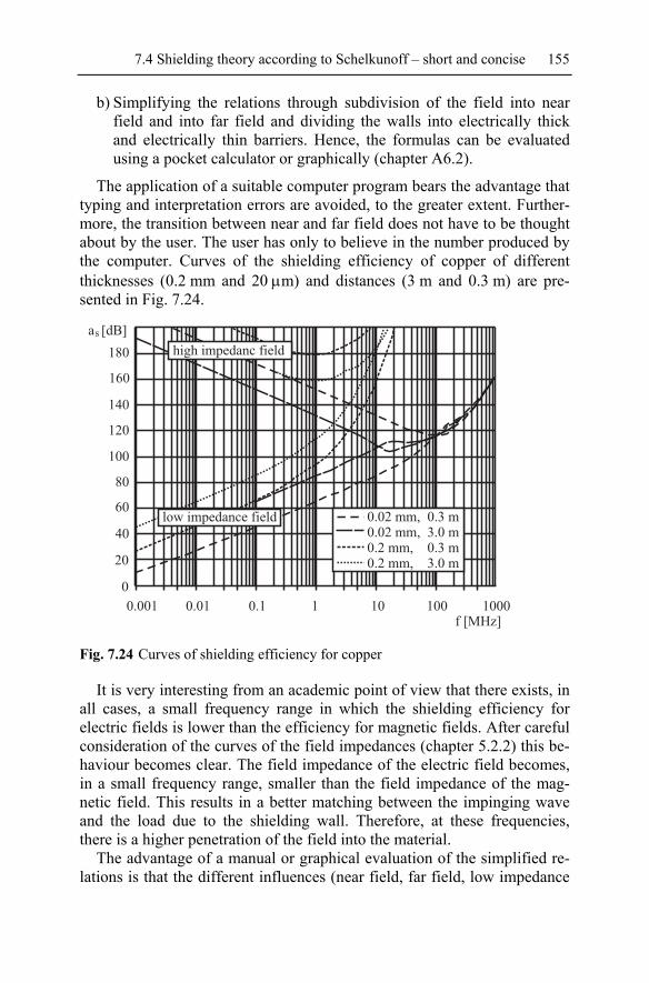
7.4 Shielding theory according to Schelkunoff – short and concise 155
b) Simplifying the relations through subdivision of the field into near field and into far field and dividing the walls into electrically thick and electrically thin barriers. Hence, the formulas can be evaluated using a pocket calculator or graphically (chapter A6.2).
The application of a suitable computer program bears the advantage that typing and interpretation errors are avoided, to the greater extent. Further-more, the transition between near and far field does not have to be thought about by the user. The user has only to believe in the number produced by the computer. Curves of the shielding efficiency of copper of different thicknesses (0.2 mm and 20 μm) and distances (3 m and 0.3 m) are pre-sented in Fig. 7.24.
high impedanc field
low impedance field 0.02 mm, 0.3 m
0.02 mm, 3.0 m
0.2 mm, 0.3 m
0.2 mm, 3.0 m
f [MHz]
0.001 0.01 0.1 1 10 100 1000
a [dB]s
180
160
140
120
100
80
60
40
20
0
Fig. 7.24 Curves of shielding efficiency for copper
It is very interesting from an academic point of view that there exists, in all cases, a small frequency range in which the shielding efficiency for electric fields is lower than the efficiency for magnetic fields. After careful consideration of the curves of the field impedances (chapter 5.2.2) this be-haviour becomes clear. The field impedance of the electric field becomes, in a small frequency range, smaller than the field impedance of the mag-netic field. This results in a better matching between the impinging wave and the load due to the shielding wall. Therefore, at these frequencies, there is a higher penetration of the field into the material.
The advantage of a manual or graphical evaluation of the simplified re-lations is that the different influences (near field, far field, low impedance

156 7 Intrasystem Measures
field, high impedance field, reflection term, absorption term) are easily observed and, furthermore, possibly provide hints for optimisation.
The computational solution should be used if only the shielding values are needed for quality control or for a simple estimation. On the other hand, shielding problems often have to be treated and moreover optimised solutions are demanded. In this case it is advisable to read and get ac-quainted with the theory of chapter A6.2.
Material properties are required in estimating the equations mentioned previously. When writing the program SHIELD, some values have been collected for materials that are used for shielding purposes.
A table of material properties together with some examples for the use of the program SHIELD are presented in chapter 7.4.1. The source code, together with the executable, is available on the homepage of the authors. The possibilities for the use of the program are shown in the following fig-ure, Fig. 7.25.
PROGRAM FOR CALCULATING THE SHIELDING EFFICIENCY VALUES OF SOME GENERIC ARRANGEMENTS
****************************************************** COPYRIGHT: Dr. Karl-Heinz Gonschorek, 01217 Dresden =================================================== Which arrangement do you wish? Id Two parallel plates against magnetic fields 1 Hollow sphere against magnetic fields 2 Hollow cylinder within a lateral magnetic field 3 Hollow cylinder within a longitudinal magnetic field 4 Plane wall (Schelkunoff), electric field 5 Plane wall (Schelkunoff), magnetic field 6 Transfer impedance of a homogeneous tube 7 Transfer impedance of a perforated tube 8 Conversion: transfer impedance <-> shielding efficiency 9 Material properties 10 Program stop 11 Id = ? Fig. 7.25 Possibilities of the program SHIELD
Exercises
Exercise 7.11: The quantity γ , Eq. (7.50), may be chosen to be

7.5 Leakages, openings, cavity resonances 157
dj 1)1( ⋅+=γ , d = skin depth
as a good approximation. Calculate the frequency fG for copper at which the relation εωκ ⋅= is satisfied. Assume that ε = ε0 = 8.854 pF/m.
Exercise 7.12: a) Express the field impedance Eqs. (7.51) and (7.52) in terms of a r/r0
dependency, with r0 = λ/2π. b) What value is obtained for r = r0 and an electric source? c) What value is obtained for r = r0 and a magnetic source?
Exercise 7.13: Express the wave impedance equations of the shielding ma-terial Γm, Eq. (7.49), in terms of d (skin depth). Interpret the result.
Exercise 7.14: Regularly, one may hear the follow statement: ‘Our cabin has a shielding efficiency of more than 100 dB!’. Why is such a statement of little value?
Exercise 7.15: An electromagnetic wave with an amplitude of 1 V/m and a frequency of f = 10 MHz is impinging on a copper wall. The source of the field is located at a distance of r = 10 m from the wall.
a) How large is the reflection coefficient ram = tam-1? b) How large is the amplitude of the current density J0 on the surface of
the copper wall?
7.4.1 Source code of the program SHIELD
The source code of the program SCHIRM, which is printed in the German version of the book, is not repeated here. However, the source code with some translation into English, now called SHIELD, is available from the home page of the authors.
7.5 Leakages, openings, cavity resonances
The total range of shielding techniques, starting with the shielding of sta-tionary magnetic fields up to the dimensioning of shields in the radar range, is difficult to describe in a closed form. Nevertheless some funda-mental statements can be made.
1. Leakages (holes) significantly influence the overall shielding of metal shields of a thickness of more than 1 mm.
158 7 Intrasystem Measures
2. Insufficient shielding values (derived from theory) in the low fre-quency range can normally be traced back to problems with the con-ductivity. This can be due to, for example, bad contacts between shielding plates, corroded door contacts, welding joints with a differ-ent conductivity to the welded plates.
3. Insufficient shielding values (derived from theory) in the higher fre-quency range can normally be traced back to real holes. In treating holes it should be remembered that the longest extension of a hole plays the decisive role.
4. If openings are necessary for ventilation purposes, for example, the following rule is valid: For any given free area (total uncovered area) a large number of small (round) holes are preferable to a small num-ber of large holes. Further information on this aspect can be found in chapter 7.6.
From statements 2. and 3. it can be noted that for the quality control of a shield it is sufficient to check the shielding effect at only two frequencies.
1. Sniffer-Method (200 – 500 kHz) – test to find bad contacts
A loop antenna into which a HF-current (200 – 500 kHz) is injected is ar-ranged around a shielding housing (cabinet). Inside all interfaces of the shielding plates and all possible leakages in the walls of the shielded space, which allow signals to penetrate, have to be inspected by a suitable sensor. This method may also be reversed by stretching a wire, into which a cur-rent is fed, diagonally between two corner points of the room. All inter-faces and possible leakages are then checked outside the shielded space. The generator inside the shielded room should be battery driven. As a sen-sor and receiver a PLL-medium wave radio can be used. A coil with an area of approximately 10 mm2, installed on a 2 to 3 m bar, will serve as a receiving antenna. Leakages due to bad contacts can be detected using this method.
2. Leakage-Test (400 MHz – 1 GHz) – test to find real holes
The housing (the cabinet) should be illuminated with a frequency of 400 MHz by an antenna suitable for that frequency. The field is measured at several positions within the shielded space (depending on the size of the room). It should become clear with only a few test points within the room whether a sufficient shielding efficiency is given or not.
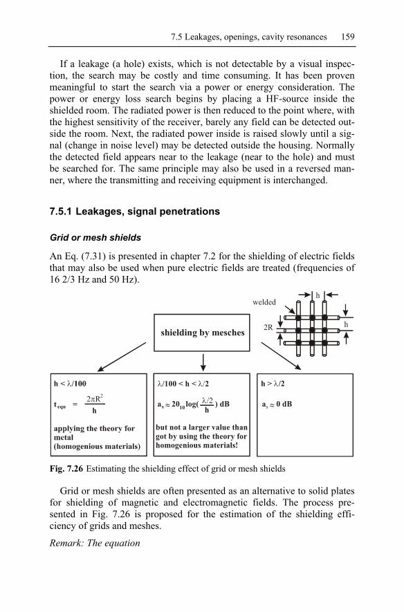
7.5 Leakages, openings, cavity resonances 159
If a leakage (a hole) exists, which is not detectable by a visual inspec-tion, the search may be costly and time consuming. It has been proven meaningful to start the search via a power or energy consideration. The power or energy loss search begins by placing a HF-source inside the shielded room. The radiated power is then reduced to the point where, with the highest sensitivity of the receiver, barely any field can be detected out-side the room. Next, the radiated power inside is raised slowly until a sig-nal (change in noise level) may be detected outside the housing. Normally the detected field appears near to the leakage (near to the hole) and must be searched for. The same principle may also be used in a reversed man-ner, where the transmitting and receiving equipment is interchanged.
7.5.1 Leakages, signal penetrations
Grid or mesh shields
An Eq. (7.31) is presented in chapter 7.2 for the shielding of electric fields that may also be used when pure electric fields are treated (frequencies of 16 2/3 Hz and 50 Hz).
shielding by mesches
welded
h
h
2R
t =equ2πR
h
λ λ/100 < h < 2 / h > /2 λ
~a ~ 20 log( ) dB a ~ 0 dB~λ/2h
but not a larger value thangot by using the theory forhomogenious materials!
2
s 10 s
Fig. 7.26 Estimating the shielding effect of grid or mesh shields
Grid or mesh shields are often presented as an alternative to solid plates for shielding of magnetic and electromagnetic fields. The process pre-sented in Fig. 7.26 is proposed for the estimation of the shielding effi-ciency of grids and meshes.
Remark: The equation

160 7 Intrasystem Measures
s 10/ 2a 20 log( ) dBh
λ= (7.53)
gets the number (7.53).
Example 7.5: The shielding efficiency of a wire mesh κ = 107 S/m) against low frequency magnetic interference fields is required. The dis-tance from the source to the shielding wall is r = 1 m and the mesh pa-rameters are R = 0.5 mm and h = 50 mm. Several cases have to be investi-gated in order to solve this problem:
a) Investigating in the range h < λ/100 1. Calculation of the equivalent metal thickness and the transition fre-
quency for which the skin depth is equal to the equivalent metal thickness: tequ = 0.031415 mm, d = tequ f = 23.6 MHz.
2. The material can be taken to be electrically thin up to the transition frequency. The shielding efficiency can be predicted in a very simple manner using
188.6 2 120 logS SS equ
ra with RR t
πλ κ
Ω= = .
This equation was derived for very thin solid materials, where RS is the DC-surface resistance of the thin material. See chapter 7.4 for further details. Taking f = 23.6 MHz yields 89 dB, with a decrease of 20 dB per frequency decade with reducing frequency.
b) Investigating in the range λ/100 < h < λ/2 Taking the grid or mesh Eq. (7.37) yields a shielding efficiency of 0 dB for h = λ/2 (frequency f = 3 GHz), which increases by 20 dB/ frequency decade with reducing frequency.
c) Drawing both results on one diagram The curves from a) and b) cross at a certain point. The result for a) should be used up to the crossing point, then subsequently the result from b) should be used. See Fig. 7.27.
Remark: There are no conditions that need to be fulfilled with respect to the distance between source and mesh. However, conditions could be de-rived from the assumption that the shielding values are only reached if the distance is larger than ten times the mesh width.

7.5 Leakages, openings, cavity resonances 161
f [MHz]
100010010
10
70
80
90
60
50
40
30
20
10.1
a [db]s
Fig. 7.27 Shielding efficiency of a wire grid or wire mesh shield against magnetic
fields
Plate with holes
In some cases metal plates with punched holes provide an alternative to grid or mesh shields. Such shields may be useful for the convection cool-ing of metallic housings containing electronical circuits.
g
h
b t
g’
For a rectangular plate of height h and width b, D becomes:
.bhD ⋅= N = total number of holes
Fig. 7.28 Plate with holes

162 7 Intrasystem Measures
The shielding efficiency against low frequency magnetic fields is given in the literature (Quine, 1957) by:
( )⎟⎟
⎠
⎞
⎜⎜
⎝
⎛⋅++=
NgD
gtdBas
3log20432][ . (7.54)
The quantities of Eq. (7.54) are shown in Fig. 7.28. Inspecting Eq. (7.54), it can be noted that the shielding efficiency is in-
dependent of the frequency. The first term of the sum represents the at-tenuation of a rectangular waveguide far below its critical frequency (cut-off frequency). Further details regarding this can be found in the proceed-ing chapter about waveguide attenuation. The 2nd and 3rd terms in the sum represent the reflection losses. The equation does not show any fre-quency dependence. Therefore, it should only be applied up to frequencies lower than 1/10 of the cut-off frequency of the individual holes. For circu-lar waveguides the cut-off frequency is given by:
bc
fcrit ⋅=
71.10
, b = inner diameter of the
circular waveguide. (7.55)
Furthermore, the equation requires that the attenuation of the material alone is much higher than the predicted attenuation due to the perforations.
Example 7.6: A perforated plate of thickness t = 1.6 mm is fixed onto an aluminium box by a HF-gasket. A receiver suitable for the frequency range 30 MHz to 250 MHz is installed inside the box.
Area of the plate h’ x b’ = 48 × 35 cm2 Area of the perforations: h x b = 40 × 30 cm2 Cross section of a single hole: g = 6 mm Distance between two holes: g’ = 25 mm
The shielding efficiency is to be predicted for 250 MHz and a low im-pedance field. Using the introduced relation leads to
.27.0,7.57
,6.343040
==
=×=×=
gtgD
cmcmbhD
Hence, the shielding is
.4.71221
7.57log20427.0323
dBdBaS =⋅++⋅=

7.5 Leakages, openings, cavity resonances 163
The total shielding efficiency including the influence of the material is usually required. The attenuation due to the material and the corresponding frequency has to be calculated (chapter 7.4) and the resulting total shield-ing can then be predicted according to Eq. (7.34).
Waveguide attenuation
If a waveguide is used far below its critical or cut-off frequency (f < 0.1 fcrit, fcrit = fg), the fields penetrating into the waveguide suffer an exponential attenuation, which can be predicted from the phase constant (propagation direction z):
zezEzE Δ⋅−⋅= α)()( 12 (7.56)
Therefore, fields having a wavelength λ >>λg (critical wave length) or a frequency f << fg (critical frequency, cut off-frequency) suffer an attenua-tion, which is proportional to the ratio between the depth and the width of the waveguide.
The following relations can be derived for a rectangular and empty waveguide with a < b (a, b = cross-section dimensions) for a frequency be-low the cut-off frequency:
μεωπαγ 2
2
−⎟⎠⎞
⎜⎝⎛==
b (7.57)
121212222
0
−⎟⎟⎠
⎞⎜⎜⎝
⎛=−⎟⎟
⎠
⎞⎜⎜⎝
⎛=−⎟⎟
⎠
⎞⎜⎜⎝
⎛=
g
gg
ff
ff
cf
λλ
λπ
λππα , (7.58)
where λg = 2b resp. fg = c0/2b.
The attenuation, in dB, of a waveguide can be expressed in the follow-ing way using the usual definition of the shielding efficiency:
l1S
2
Ea 20 log 20 log e 8.686 l, l z,E
α= = = α = Δ (7.59)
2g
S
f2a 8.686 l f 1 dBc f
⎛ ⎞π= ⋅ ⋅ ⋅ ⋅ −⎜ ⎟
⎝ ⎠. (7.60)

164 7 Intrasystem Measures
For f = fg, the attenuation becomes zero. For f << fg or λ >> λg, the -1 under the root may be neglected and the attenuation can be approximated by
blaS 27= . (7.61)
The attenuation values for a number of waveguide types are shown in Fig. 7.29.
aS = 27 l/b [dB] λg = 2 b (7.62)
aS = 32 l/b [dB]
λg = 1.71 b (7.63)
b
b
b
b
l
aS = 30 l/b [dB]
λg = 1.8 b (7.64)
Fig. 7.29 Waveguide attenuation for different waveguide types
Considering n parallel honey combs, for instance, yields the result:
nblas log2030 10⋅−⋅= . (7.65)
Remark: This formula implies a phase and vector superposition of the fields of all single honey combs, so is very suitable for a ‘worst case’ esti-mation. However, the relation loses validity when considering a very large number of parallel combs.
The equations of the waveguide attenuation are only provisionally use-ful for estimating the shielding efficiency, because they only describe the attenuation of the field inside the waveguide. The additional attenuation due to the coupling from the free field to the guided field is not considered. It can be stated with respect to Schelkunoff’s shielding theory that only the attenuation due to absorption is considered, the attenuation caused by re-flections is neglected.

7.5 Leakages, openings, cavity resonances 165
Nevertheless, the waveguide approach is very well suited to the consid-eration of penetrations and non-electric interfaces that have to be installed into the shielded area. The values predicted by Eqs. (7.59) and (7.62) to (7.64) are reached in any situation. Consider the case whereby compressed air has to be brought into a shielded space by a ¾-inch hose. It is sufficient to weld a metallic tube of 3 inches in length (7.5 cm) into the shielding wall in order to maintain the overall shielding efficiency of 100 dB of the cabin. According to Eq. (7.63), a tube, which is 4 times as long as its inner diameter, has a waveguide attenuation of 128 dB (far below its cut-off fre-quency).
Waveguide attenuation considering the losses given by the wave mismatch
An equation (cut to numerical values) is given in the literature (taken from seminar records, originator not known) for estimating the shielding effi-ciency of a rectangular wave guide, considering also the reflection losses. The equation is reproduced here for completeness:
LD
SL
MHzf
mmLdBas 30ln1log20log20100][ +⎟⎟
⎠
⎞⎜⎜⎝
⎛⎟⎠⎞
⎜⎝⎛+⋅+⎟
⎠⎞
⎜⎝⎛⋅−= (7.66)
The scope of this equation is specified as the range where L < λ/2. The quantities in the equation are shown diagrammatically in Fig. 7.30.
S
L
D
Fig. 7.30 Observation window within a shielding wall
Treating the parts of the equation individually the following explanation can be stated:
⎟⎠⎞
⎜⎝⎛⋅−
MHzf
mmLlog20100 10 , (7.67)

166 7 Intrasystem Measures
far field reflection part considering the mismatch between the wave im-pedance Γ0 and the surface impedance ΓLoch ;
⎟⎟⎠
⎞⎜⎜⎝
⎛⎟⎠⎞
⎜⎝⎛+⋅
SLln1log20 10 , (7.68)
term of the sum representing the shape of the opening;
LD30 , (7.69)
term due to the waveguide attenuation.
Regarding the far field reflection part, it should be noted that the at-tenuation relates to a plane in the far field. Furthermore, it should be noted that only the influence of the leakage has been considered. The shielding material should have a shielding efficiency much higher than the attenua-tion of the observation window.
Example 7.7: The far field attenuation at a frequency of f = 100 MHz for an opening with the dimensions L = 10 cm, S = 3 cm and D = 5 cm has to be predicted.
According to Eq. (7.66) a value of 61.9 dB is calculated.
Summary
In order to use the different procedures discussed the following strategy is recommended:
1. If a penetration or hole into a shielded area is required for the trans-port of non conducting media (pressured air, optical cable, shaft of synthetic material or similar), it is normally sufficient to work with the attenuation given by waveguide theory, i.e. Eqs. (7.59) to (7.64).
2. If an opening for observation, service or handling is required and the overall height of the waveguide is significant, the Eq. (7.66) for the attenuation of a waveguide including wave impedance mismatch losses should be applied.
3. If two or more holes (number n), located near to each other, are in-stalled, the relation for the waveguide attenuation with or without the mismatch losses for a single hole should be used at first. Subse-quently, the prediction of the total influence of all holes can be per-formed through a linear superposition:

7.5 Leakages, openings, cavity resonances 167
naa SEsges log20 10⋅−= . (7.70)
4. If a large number of holes (for ventilation or lighting purposes) is re-quired, the relations of a plate with holes, Eq. (7.54), should be used. Alternatively, the relation for wire meshes, Eq. (7.53), considering the low frequency range can be used. The choice of relation is de-pendent on the real execution of the penetration plate.
Coupling-in and coupling-out calculations using Babinat’s principle
A more thorough treatment of the electromagnetic coupling through open-ings, holes and slots can be found in the literature [Le/Mo04] and [Me78].
7.5.2 Low frequency resonances, cavity resonances
Low frequency resonances
A lack of homogeneity within the shielding box may lead to low frequency resonances. Unequal phase shifts in the wave transmission from one side to the other on two or more different ways may lead to constructive or de-structive superposition. This situation occurs if, for example, one ray pene-trates through the material and another through a gap clearance. See Fig. 7.31.
SE E= E e = e eE
Ek EE
- t - t -j t
1M
1L1L2L
1M 1M2M
t
Fig. 7.31 Propagation in two different ways
Assuming that the phase shift due to the material occurs according to the theory of the skin effect and that the wave through the air gap does not suf-fer a noticeable phase shift, it is possible that a measurable superposition occurs in the inner region of the shielded area. The first resonant frequency (destructive superposition) corresponds to the case where the phase shift, based on the theory of the skin effect, amounts to 180°. Theoretically, a

168 7 Intrasystem Measures
resonance occurs at every uneven multiple of 180°, which does normally not show any remarkable effect in reality.
The lowest resonant frequency occurs when ( ) :180 delayt °= πβ
rrmmr
fjtjjßt
ttfeee
κμμκ
πμκππ2
4
21039.4 ⋅
==→== (7.71)
Example 7.8: The lowest resonant frequency is needed for a shielding en-closure made of 0.8 mm aluminium plates and one made of 0.8 mm steel plates.
HzfmmtFekHzfmmtAl
rrr
rrr3921000,175.0,8.0:1141,60.0,8.0:
=→====→===
μκμκ
The shielding efficiency below the first resonant frequency is well de-fined by the given equations. Below the resonance, but near to it, the at-tenuation is larger than predicted by theory. It has to be noted, however, that this effect is not very significant and has only to be considered in spe-cial cases.
Standing waves, cavity resonances
More attention has to be paid to the effect of standing waves in the high frequency range. Internal reflections within a cuboid or a cabinet with 6 walls (Fig. 7.32) lead to standing waves.
b
a
Fig. 7.32 Box to be considered as a cavity resonator
The cavity resonances (derived from the theory of waveguides) occur at
,2
222
⎥⎥⎦
⎤
⎢⎢⎣
⎡⎟⎠⎞
⎜⎝⎛+⎟
⎠⎞
⎜⎝⎛+⎟
⎠⎞
⎜⎝⎛=
lk
bn
amcfr (7.72)
7.5 Leakages, openings, cavity resonances 169
,][][][
150][222
⎟⎟⎠
⎞⎜⎜⎝
⎛+⎟⎟
⎠
⎞⎜⎜⎝
⎛+⎟⎟
⎠
⎞⎜⎜⎝
⎛⋅=
mlk
mbn
mamMHzfr (7.73)
a,b,l = lengths of the side walls, c = speed of light, m, n, k = 0,1,2,3...integers, independent from each other, where not
more than one can be zero in order to get a resonance. Tak-ing m = 1, n = 0 and k = 1 yields a TE101resonance.
It can be observed for a fixed size of cavity that resonances occur more and more frequently with increasing frequency. In this context it is useful to talk in terms of modes and define a mode density, which describes the number of resonances or modes within a frequency decade.
The special case where ( )metresa b l w≈ ≈ ≈ gives lowest order degener-
ate TE011, TE101 and TE110 resonances with a frequency of
.121212150ww
fMHz ⋅=⋅⋅= (7.74)
Example 7.9: Housing with w = 0.3 m MHzfr 707
min=→
Example 7.10: Cabinet for 19“ plug-in units with MHzfmlmbma r 22176.0,56.0,52.1
min=→===
Example 7.11: Shielded chamber with MHzfmlmbma r 4.481.6,6.3,5.2
min=→===
Example 7.12: EMC cabin (shielded) with MHzfmlmbma r 3.884.2,8.1,4.2
min=→===
Remark: Boxes and cabinets with quality factors of 100 up to 1000 (typical quality factor of empty cavities) suffer from cavity resonances with reductions in the shielding efficiency of up to 60 dB.
Exercises
Exercise 7.16: A shielded rectangular channel (20 x 40 cm2) with a length of 10 m length is installed between two shielded areas. The channel is welded at both ends into the shielding walls in a highly conductive man-ner. The shielding effect of the channel has to be validated within the framework of quality control. Make a proposal describing a procedure for

170 7 Intrasystem Measures
executing a sniffer test, as well as a method for the execution of a leakage test.
Exercise 7.17: A cabin shield is constructed using a grid (wire mesh shield) with quadratic cells. The grid consists of wires all welded to each other at their crossing points. The wires have a diameter of 0.5 mm and are spaced apart by 3 cm. The wires have a conductivity κr = 0.17. The dis-tance between the mesh in the ceiling and in the floor amounts to 2.8 m.
a) How large is the shielding efficiency against static electric fields (chapter 7.2)?
b) How large is the shielding efficiency against low frequency electric fields of 50 Hz, if the field source is 20 m away from the grid (use Schelkunoff’s theory)?
c) Explain the apparent discrepancy between the results of a) and b). d) How large is the shielding efficiency against low frequency magnetic
fields of 50 Hz, if the field source is 20 m away from the grid? e) How large is the shielding efficiency against signals from a GSM-900
(900 MHz) mobile phone, if the mobile phone is used at a distance of 30 cm from the shielding grid?
Exercise 7.18: A hose for pressured air has to be brought into a shielded EMC-cabin. The supply hose has an outer diameter of 24 mm. It is planned to bring the hose into the shielded area via a shielding tube with an inner diameter of 30 mm. The shielding tube is intended to be welded into the shielding wall. How long must the tube be to achieve the required shield-ing efficiency of 120 dB at f = 1 GHz?
Exercise 7.19: A screened cubical for measuring purposes has inner di-mensions of 4 x 4 x 3 m3. Predict the frequencies of the first 5 cavity reso-nances.
Exercise 7.20: A circular waveguide, with a length to diameter ratio of 3, is welded into a shielding wall. The waveguide is operated far below its critical frequency (cut-off frequency).
a) How large is the attenuation of the signals by the wave guide? b) It is intended that the waveguide is to be replaced by 4 identical circu-
lar waveguides. The waveguides will have the same total cross sec-tion and the same length as the original waveguide. How large is the total attenuation of the new arrangement? Assume a linear superposi-tion of the field.
c) How long must the 4 waveguides be in order to achieve the same total attenuation as the single waveguide calculated in a)?

7.6 Cable coupling and cable transfer impedance 171
Exercise 7.21: a) At what frequency can the low frequency resonance be expected
within a shielding box made from 4 mm thick aluminium? b) How large is the field attenuation due to the material at the resonant
frequency (only the absorption part)?
7.6 Cable coupling and cable transfer impedance
The term cable coupling means the coupling of an electromagnetic signal into a cable, the coupling out of a cable and also the outer coupling from one cable to another. In chapter 7.6.1 the basic models of cable coupling are presented and formulas for the coupling are stated. Chapter 7.6.2 treats, in a very concise manner, the coupling into un-twisted and twisted cables. The coupling into a shielded cable and the corresponding cable transfer impedance are dealt with in chapter 7.6.3. A simple procedure is described for predicting this value in annex A9. Finally, chapter 7.6.4 deals with the treatment of cable shields at the penetration into an equipment box.
7.6.1 Cable coupling
The following highly simplified models have to be investigated. Coaxial cables are depictured in the models. In addition, un-twisted and twisted two-wire lines are considered.
Coupling: field to cable
Selectromagnetic fieldfrom an antenna,plane wave
UStör1 UStör2
→
Fig. 7.33 Model of the field to cable coupling

172 7 Intrasystem Measures
An electromagnetic field from an external source couples into an inter-face cable, and produces undesired interference signals at the device inputs and outputs.
Coupling: cable to antenna
S→
SignalU UInterference Fig. 7.34 Model of the coupling cable to antenna
A desired signal and its harmonics in an interface cable produce an elec-tromagnetic field. This signal is received by the antenna and superimposes to the desired signal within the receiver.
Coupling: cable to cable
In the following model, the two preceding models are combined. The de-sired signal and its harmonics in an interconnecting cable produces an electromagnetic field. This field couples to a second non-involved cable, producing interference signals at the inputs and outputs of the circuits con-nected by this cable. This model is presented in Fig. 7.35. Predefined pa-rameters are labelled for results presented later, where both cables are taken to be the type RG 58 CU.
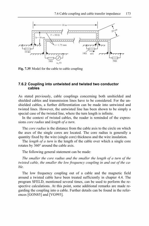
7.6 Cable coupling and cable transfer impedance 173
10 m
20 cm
h = 10 cmΓ = 50 Ω
r = 1.75 mm.10 kΩ 10Ω.
50Ωu 0 (t)
.u(t) .
50Ω
Fig. 7.35 Model for the cable to cable coupling
7.6.2 Coupling into untwisted and twisted two conductor cables
As stated previously, cable couplings concerning both unshielded and shielded cables and transmission lines have to be considered. For the un-shielded cables, a further differentiation can be made into untwisted and twisted lines. However, the untwisted line has been shown to be simply a special case of the twisted line, where the turn length is infinite.
In the context of twisted cables, the reader is reminded of the expres-sions core radius and length of a turn.
The core radius is the distance from the cable axis to the circle on which the axes of the single cores are located. The core radius is generally a quantity fixed by the wire (single core) thickness and the wire insulation.
The length of a turn is the length of the cable over which a single core rotates by 360° around the cable axis.
The following general statement can be made:
The smaller the core radius and the smaller the length of a turn of the twisted cable, the smaller the low frequency coupling in and out of the ca-ble.
The low frequency coupling out of a cable and the magnetic field around a twisted cable have been treated sufficiently in chapter 4.4. The program SFELD, mentioned several times, can be used to perform the re-spective calculations. At this point, some additional remarks are made re-garding the coupling into a cable. Further details can be found in the refer-ences [GON85] and [VG993].

174 7 Intrasystem Measures
In handling the coupling into a cable two frequency ranges have to be considered separately:
1. The low frequency range where the cable length L is electrically short (L < 0.1 λ, λ = wavelength of the frequency f under considera-tion)
2. The high frequency range
For the low frequency range, the programs described in this book can be used. From the physical law M12 = M21 (the mutual inductance between circuit 1 and circuit 2 is equal to the mutual inductance between circuit 2 and circuit 1) models can be developed, which describe the coupling-in process very well. However, this procedure can only be used if all quanti-ties of the coupled circuits and the influenced circuit can be described to sufficient precision.
For a zero order estimation, which has to be considered tentatively, the usual approach of a so-called half remainder length of turn is completely sufficient. A view onto a twisted cable, which is located in a homogeneous sinusoidal magnetic field, is shown in Fig. 7.36.
B
Fig. 7.36 View from above onto a twisted cable located within a homogeneous
magnetic field
Plus and minus signs can be seen in the figure within the influenced ar-eas of the twisted cable. These signs point to the fact that the normal direc-tion of the influenced area is rotated by 180° degrees at every half-length of a turn. This concept leads to the fact that no coupling-in occurs for an even number of influenced areas. Conversely, an odd number leads to maximum coupling, which, if the magnetic flux density B is known, can be predicted by the following approximation:
i turn centerU l r Bω= (7.75)
lturn = length of a 360°-turn, rcenter = radius from the wire axis to the middle axes of the single cores.
7.6 Cable coupling and cable transfer impedance 175
More precise calculations predict a level of safety that cannot be guaran-teed.
It is often attempted to get exact results within the high frequency range using HF-simulation programs. Aside from the fact that the expenses are very high, this approach is only justified for parameter studies. In the HF-region it is more important than in the LF-region that uncertainty associ-ated with the quantities influencing the coupling process (twisting, position of the single wires or cores, output and input impedances of the connected electrical circuit) require that every simulation result must be queried. At this point, a pragmatic method of estimation is presented. This method consists of taking three cases into account.
1. Connection of unsymmetrical circuits by twisted or untwisted pairs of wires: Coupling in the same way as for single wire connections with ground return.
2. Connection of symmetrical circuits without any special measures for balancing: Calculation of a coupling in the same way as single wire connections with a ground return, considering an unsymmetry at-tenuation of 20 dB. More accurately, it should be better termed a symmetry attenuation.
3. Connection of highly symmetrical circuits with special measures for balancing: Calculation of a coupling in the same way as single wire connections with a ground return, considering an unsymmetry at-tenuation of 40 to 60 dB.
The unsymmetrical attenuation is defined by the conversion of a com-mon mode signal into a differential mode signal:
UCMa 20 log
unsym UDM
= ⋅ . (7.76)
UCM is the voltage of the single wire arrangement against ground, UDM is the voltage occurring between the cores.
7.6.3 Coupling into and between shielded cables
It is assumed, within all the following considerations, that the shields of the cables have such an efficiency that the coupling ‘outer cable shield to core’ and ‘core to outer cable shield’ can be considered to have no re-reaction.

176 7 Intrasystem Measures
The coupling into a cable, as well as the coupling out of a cable, are de-scribed by the cable transfer impedance TZ ' . The coupling due to the cable transfer admittance Y’T is not considered here.
In order to perform a calculation in the frequency domain, only the magnitude of the cable transfer impedance is required. Calculations in the time domain (pulse coupling), however, require the complex value of the transfer impedance, meaning both the magnitude and the phase.
Analyzing the coupling-in process
The analysis of the coupling into a shielded cable is executed in the fol-lowing way:
1. Prediction of the current I(l) on the outer surface of the cable screen. 2. Placing of longitudinal voltage sources of
dlZlIldU T')()( ⋅= (7.77)
inside the cable. 3. Calculating the process inside the cable using the transmission line
theory, considering distributed sources.
The connection between the frequency domain and the time domain is given by Fourier analysis, more specifically the Fourier transform.
1. Prediction of the current I(l) on the outer surface of the cable
a) Low frequency approximation
- Electric field
The voltage to ground of a wire, as drawn in Fig. 7.37, is approximated to a first-order estimation through multiplication of the height h of the wire by the field strength E at the position of the wire.
El
2RI
2
I
2h
Fig. 7.37 Model for the electric coupling

7.6 Cable coupling and cable transfer impedance 177
In the case that both ends of the wire (double-sided connection of the cable shield) are connected to ground, the capacitive current flows in equal parts to the left and right hand sides. If only one side is connected to ground, the total current flows in that direction only,
RhlChECI 2ln
2, πεω ≈= . (7.78)
- Magnetic field
The driving voltage for the current of the circuit in Fig. 7.38 is defined by the induction law.
H
l
I Ih
Fig. 7.38 Model for the magnetic coupling
If this voltage is short-circuited, a current flows, which is limited, to a first-order approximation, by the effective impedance Z = R + jωL of the outer circuit. In the very low frequency range the resistance, R, limits the current. However, in the medium frequency range the inductive part, ωL, governs the current,
RhlL
LHlhI 2ln
2,
πμμ
≈= . (7.79)
- Inductive coupling between two lines
The current of loop 1 in Fig. 7.39 produces a magnetic flux within the loop 2, which induces a voltage in this loop 2. If, as before, this voltage is short-circuited, a short circuit current flows. The impedance of the second circuit provides the current limiting factor in this case. In the very low frequency range the resistance determines the magnitude of the short circuit current. Furthermore, the self inductance governs the current in the medium and high frequency range.

178 7 Intrasystem Measures
2rI2 I222h
d
I1I1h1
M
Fig. 7.39 Model for the inductive coupling between two lines
Neglecting the reaction from loop 2 to loop 1 leads to the following ex-pression:
( ) ( )( ) ( )
2
2
212
22
212
22
12
12 2ln
ln
rh
hhrdhhrd
ILMII
−+−++−
⋅=⋅= (7.80)
( )ldhhlll <<== ,,, 2121 (7.81)
b) High frequency solutions
- Computer simulations
An example is given in chapter 6.4.3 for approximating the coupling into a loop installed in the vicinity of a short electric antenna. The evaluation is costly, but is beneficial in the understanding of fields in the near field re-gion of antennas. Today, such arrangements build from antennas, loops, and secondary radiators are analysed using respective computer programs.

7.6 Cable coupling and cable transfer impedance 179
d = 0.03 m1h
= 1
2 m
1
h =
0.1
m2 d =
0.0
1m2. . .
a = 5 m
I2
l = 2 m2
Fig. 7.40 Example arrangement for a computer simulation
The arrangement in Fig. 7.40 has been investigated using the program CONCEPT. It is the same arrangement as that treated in chapter 6.4.3. The current on the right hand side of the cable connection to ground is shown in Fig. 7.41. The current data of the whole loop is available within the out-put file of the respective CONCEPT-simulation.
7.0 12.0 17.0 22.0 27.0f [MHz]
0
0.01
0.02
2.0
I = f (f) for aradiated power of 100 W
2
I [A]2
Fig. 7.41 Current via the right hand cable connection to ground
- Transmission line theory (transmission line above lossy ground)
Assume that the coupling into a very long cable, which is possibly ar-ranged above a lossy ground, has to be predicted. Transmission line the-

180 7 Intrasystem Measures
ory, applying distributed sources, has proven to be a very valuable tool for understanding such arrangements. Apart from the fact that an analytical so-lution for the current and the voltage of a transmission line above ground can be obtained, the solutions also deliver deeper insights into the coupling processes taking place. To highlight this concept, the following situation may be considered: An electromagnetic wave incident on a transmission line has, depending on the angles with respect to the transmission line, a different propagation speed to the wave produced on the transmission line. Constructive and destructive superpositions occur, which produce a par-ticular kind of antenna diagram (directivity function).
The following analysis can be deduced: If a plane electromagnetic wave, defined by its Poynting vector and the direction of the electric field strength, is impinging onto a horizontal conductor, a current is coupled onto this wire. Furthermore, if this conductor forms a transmission line (a transmission line above conducting ground in this special case), the cou-pled current propagates in the form of a line wave on the transmission line with its characteristic propagation speed.
Imagining an electromagnetic wave, whose Poynting vector forms a cer-tain angle with the transmission line; it becomes clear that the propagation speed of the wave, in the direction of the transmission, is smaller than the speed of light. This process implies that a time delay occurs between the wave coupled onto the transmission line and the initial electromagnetic wave.
The transmission line arrangement presented in Fig. 7.42 is used in the following mathematical derivations.
x
transmission line
y
z
h
S
2zz1 ϕ
ψ
→
Fig. 7.42 Model for predicting the single wire current via the transmission line
theory

7.6 Cable coupling and cable transfer impedance 181
The angle ϕ describes the angle between the Poynting vector and the positive z-axis (angle within the ground plane) and ψ is the elevation angle to the ground plane. The yz-plane is the conductive ground. In order to clearly analyse the coupling into a horizontal line above a lossy ground plane, a number of assumptions are made. It is assumed in the following derivations, that the conductivity σ of the ground (conductive ground) is sufficiently high to fulfil the condition σ > ωε for all frequencies of inter-est.
Example 7.13: For soil (natural ground) with a conductivity of σ = 10-2 S/m, σ becomes σ = ωε at f = 180 MHz.
In analysing the coupling of an electromagnetic wave (see Fig. 7.43) into a transmission line above ground, the driving voltage is considered to be distributed along the whole line length. The effective voltage, for a very small piece of the line, is calculated from the electric field strength in line direction multiplied by the length of this small piece. For the line shown in Fig. 7.42, this yields
dzEU z−=Δ . (7.82)
Δ
+
∼I -Ez d
d
z
z
dz
Z′
Y′ UU
U
∂z∂U dz
+ Iz
∂∂ dzI
Fig. 7.43 Equivalent circuit for a small piece of wire orientated in the z-direction,
illuminated by an electromagnetic wave
The transmission line parameters Z’ and Y’ are predicted, to a first order approximation, in the same way as in the classical transmission line theory. For the arrangement in Fig. 7.44, for instance, the following equations can be derived:
ahL 2ln
20' ⋅=
πμ (7.83)
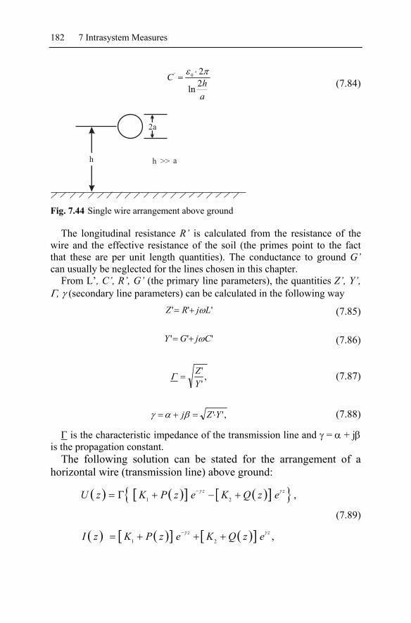
182 7 Intrasystem Measures
ahC 2ln
20' πε ⋅= (7.84)
h
2a
h >> a
Fig. 7.44 Single wire arrangement above ground
The longitudinal resistance R’ is calculated from the resistance of the wire and the effective resistance of the soil (the primes point to the fact that these are per unit length quantities). The conductance to ground G’ can usually be neglected for the lines chosen in this chapter.
From L’, C’, R’, G’ (the primary line parameters), the quantities Z’, Y’, Γ, γ (secondary line parameters) can be calculated in the following way
''' LjRZ ω+= (7.85)
''' CjGY ω+= (7.86)
,''
YZ
=Γ (7.87)
,'' YZj ⋅=+= βαγ (7.88)
Γ is the characteristic impedance of the transmission line and γ = α + jβ is the propagation constant.
The following solution can be stated for the arrangement of a horizontal wire (transmission line) above ground:
( ) ( )[ ] ( )[ ]
( ) ( )[ ] ( )[ ]
1 2
1 2
,
,
z z
z z
U z K P z e K Q z e
I z K P z e K Q z e
γ γ
γ γ
−
−
= Γ + − +
= + + +
(7.89)
7.6 Cable coupling and cable transfer impedance 183
with
( ) ,2
110
dzEezP z
z
z
z∫= γ
Γ (7.90)
( ) dzEezQ z
z
z
z∫= −2
021 γ
Γ (7.91)
( ) ( )( ) ( ) ,
1221
12
21
2221
11 zzzz
zzz
erreezQezPrerK
−−−
−
−−
= γγ
γγγ
(7.92)
( ) ( )( ) ( ) ,
1221
12
12
1112
22 zzzz
zzz
erreezPezQrerK−−−
−−
−−
= γγ
γγγ
(7.93)
1 21 2
1 2
, ,Z Zr rZ Z
− Γ − Γ= =
+ Γ + Γ (7.94)
Γ = characteristic impedance of the line, γ = propagation constant of the line,
21, ZZ = load impedances of the line, Z1 at the beginning, Z2 at the end.
Ez in Eqs. (7.90) and (7.91) represents the undisturbed field strength, which is the field that would be given at the position of the line if the line were not present. The total “undisturbed” field at the position of the con-ductors consists of the impinging field with the amplitude Eo and the field reflected at the ground plane (the surface of the earth in this case).
The following equations can be stated:
z 0jk2h sin jkzcos cosE (h,z) E sin cos (1 R e )eν
− ψ − ψ ϕ= ψ ϕ − , (7.95)
for a vertically polarized wave (vector of the magnetic field strength paral-lel to the ground plane) and
ϕψψϕ coscossin20 )1(sin),( jkzhjk
hz eeREzhE −−+= , (7.96)
for a horizontally polarized wave (vector of the electric field strength par-allel to the ground plane.
184 7 Intrasystem Measures
The phase of the field strength is related to the phase of the impinging wave at z = 0 and x = h.
The constant k is the free space propagation constant given by
λπεω 2
=μ= ook (7.97)
and Rv and Rh are the reflection coefficients of the wave at the surface of the ground (earth).
The reflection coefficients can be calculated using
ψωεσεψ
ωεσε
ψωεσεψ
ωεσε
2
2
cos)1(sin)1(
cos)1(sin)1(
−+++
−+−+=
jj
jjR
rr
rr
v (7.98)
and
ψωεσεψ
ψωεσεψ
2
2
cos)1(sin
cos)1(sin
−++
−+−=
j
jR
r
r
h (7.99)
For incident plane waves, as they have been implicitly defined with the Eqs. (7.95) and (7.96), the Eqs. (7.90) and (7.91) can be solved straight-forwardly. The result is the closed form solution of Eq. (7.89). However, through this procedure the dearness gets lost.
Considering the special case of a coupling into a semi-infinitely long open line, illustrative relations can be produced. The semi-infinitely long line may be considered as a line that extends from the left hand side in re-lation to Fig. 7.41, being very long and ending at z = 0. The open circuit voltage UL at z = 0 is required.
Approximate solutions can be derived for this open circuit voltage UL. The derivations of these solutions, and a deeper insight into the coupling into horizontal transmission lines above lossy ground, can be found in the publication [VAN78].
In a compact notation the following solution can be stated:
.)(sin21),( 1, o
otjo
otj
hvoL Ej
ejeDcU
⎪⎭
⎪⎬⎫
⎪⎩
⎪⎨⎧
+−
=−
±−
ωψ
σε
ωϕψ
ωω
(7.100)
The vertical and horizontal polarizations differ only by the factor Dv,h and the exponent of the factor (sin ψ). The factor Dv,h represents the so-

7.6 Cable coupling and cable transfer impedance 185
called directivity functions for the vertical (Dv) and the horizontal (Dh) po-larization. For the vertical polarization, the value of -1 as exponent of the sinψ has to be chosen, and for the horizontal polarization, the value of +1. The quantity t0 (time delay between the direct strike and the strike of the wave reflected at the plane) is calculated by
ocht ψsin2
0 = (7.101)
The directivity function of the vertical polarization reads
ϕψβω
αϕψϕψ
coscos
cossin),(−+
=
kjc
Do
v (7.102)
and of the horizontal polarization
ϕψβω
αϕϕψ
coscos
sin),(−+
=
kjcD
oh , (7.103)
c0 is the speed of light and α, ß are quantities from the Eq. (7.88).
For a lossless line above a lossless ground, α becomes 0 and β is given
by β = k =λπ2 , resulting in the directivity functions
ϕψϕψϕψ
coscos1cossin),(
−=vD (7.104)
and
ϕψϕϕψcoscos1
sin),(−
=hD (7.105)
These directivity functions (for α = 0) are shown for several ascent an-gles in Fig. 7.45.

186 7 Intrasystem Measures
2
3
4
5
270300
330
= 0
30
6090
120
150
180
210
240
= 20 0
0000
0
ψ
ψψ
ψψ
= 20= 30= 45= 600ψ= 60
ϕ
.
a)
2
270300
330
30
6090
120
150
180
210
240
= 20 0
0
0000ψ
ψψ
ψψ
= 20= 30= 45= 60
0ψ = 60
1
= 0ϕ
Richtfunktionen, a) vertikale Polarisation, b) horizontale Polarisation
b)
H
H
S
E
E
Fig. 7.45 Directivity functions, a) vertical polarization, b) horizontal polarization
Reminder: Longitudinal voltage sources are used in the derivation of the voltages coupled into the line; the voltages are calculated from the electric field strength in direction of the transmission line.
Interpreting the directivity function of the vertical polarization (H-vector within the reflection plane) and the angle ϕ = 0° in the reflection plane, it can be seen that the maximum of the direction function increases with de-creasing elevation angle ψ. The external wave and the coupled wave run in

7.6 Cable coupling and cable transfer impedance 187
the same direction towards the open circuited end and the external wave couples permanently energy into the transmission line. The propagation velocity of the external wave and the wave on the line become more and more the same.
Observing the directivity function of the horizontal polarization (E-vector within the reflection plane), troughs can be seen at ϕ = 0° and ϕ = 180°. The E-vector becomes zero at these angles, with respect to the direction of the transmission line.
1000
100
10
1
0.1
0.01 0.1 1 10 100
f [MH z ]= vertical polarization
polarization= horizontal
[V/V
/m]
U 1 V
/m *
D(3
0, ϕ
)
Fig. 7.46 Open circuit voltage of a semi-infinitely long transmission line, height
of the line above ground h = 10 m, elevation angle ψ = 30°, conductivity of the soil σ = 10-2 S/m
It is possible to predict the open circuit voltage of a semi-infinitely long transmission line using Eq. (7.100). Assuming a value of 1 V/m for the electric field strength E0 and relating the open circuit voltage to the direc-tivity factor, a representation of this open circuit voltage is possible with Ψ

188 7 Intrasystem Measures
as the parameter. In order to show the influence of the limited soil conduc-tivity on the amplitude of the voltage and also the amplitude of the current, these voltages are plotted as function of frequency for two different con-ductivities in Fig. 7.46 and Fig. 7.47. The height of the transmission line above ground is 10 m in all cases.
1000
100
10
1
0.1
0.01 0.1 1 10 100
f [MH z ]= vertical polarization
polarization= horizontal
[V/V
/m]
U 1 V
/m *
D(3
0, ϕ
)
Fig. 7.47 Open circuit voltages of the semi-infinitely long transmission line,
height of the line above ground h = 10 m, elevation angle Ψ = 30°, soil conductivity σ = 10-3 S/m
2. Assumption of longitudinal voltage sources
Having predicted the current on the cable screen, longitudinal voltage sources have to be placed in the influenced signal circuit under the screen. This is achieved using the procedure outlined in the following steps with relation to Fig. 7.48.
The currents I1 to I5 in a) correspond to the known currents on the screen, which can be specified for each position. Subsequently, the open

7.6 Cable coupling and cable transfer impedance 189
circuit voltage for the influenced signal circuit are then calculated from these currents according to
dzzIZUd Ti ⋅⋅= )(' (7.106)
Within a numerical calculation, the infinitesimal small sources dUi be-come finite sources ΔUi. The integration becomes a summation. The value ZT’ is the cable transfer impedance, which will be explained in more detail shortly. This quantity combines the current on the screen with the voltage between a core line and the cable screen inside the cable.
x xx
xxI1 I2 I3
I4I5
dU3dU1 dU2 dUN
Γ
IL2IL1
Z UL1 ZL2UL2L1Γ
~ ~ ~ ~ ~ ~ ~
IiU
U
i
i
= ZT z. .’
a)
b)
c)
Fig. 7.48 Model of the coupling process from the current on a cable screen into a
voltage between the core line and the screen within the cable
3. Calculation of the propagations on the signal line under the screen
In order to calculate the voltages across the load impedances ZL1 and ZL2, it is again possible to specify a substituting circuit representation for an in-finitesimally small piece of the transmission line. The substituted circuit has the same form as the circuit of Fig. 7.41, only that the longitudinal

190 7 Intrasystem Measures
source –Ez dz is now substituted by dzzIZUd Ti ⋅⋅= )(' . The load voltages become:
( ) ( )[ ] ,sinhcosh' 20
11 dzzlZzlIZ
DZU L
l
TL
L −+−∫−= γγΓ (7.107)
[ ] ,sinhcosh' 10
22 dzzZzIZ
DZU L
l
TL
L γγΓ +∫= (7.108)
( ) ( ) lZZlZZD LLLL γΓγΓΓ sinhcosh 212
21 +++= . (7.109)
Assuming the discretization mentioned above, the integration becomes a summation and resultant equations stated below are yielded.
( ) ( )[ ] ∑ −+−−=i
iLiiL
L zlZzlUD
ZU ,sinhcosh 21
1 γγΓΔ (7.110)
[ ] ∑ +=i
iLiiL
L zZzUD
ZU ,sinhcosh 12
2 γγΓΔ (7.111)
,' zZIU Tii ΔΔ = (7.112)
Γ = characteristic impedance, γ = propagation constant of the influenced signal line.
Proposal for a first-order estimation of the voltage coupled into a coaxial cable within the frequency range
The procedure described above for determining the voltage coupled into a shielded cable, is very costly. The expenses are only justified if trustwor-thy input data is available for the coupling quantities. Within the concep-tual phase of a project, or for a first-order approximation in the sense of an exclusion procedure, it is often sufficient to make a simple estimation. The procedure described below may produce relatively usable results:
1. Fixing the cable length l which will be influenced.
2. Fixing the possible current I on the cable screen (value measured or predicted, limit value).

7.6 Cable coupling and cable transfer impedance 191
3. Using a cable transfer impedance of |ZT’| = 10 mΩ/m in the fre-quency range up to 1 MHz and using a cable transfer impedance of
][/10' MHzfmmZT ⋅= Ω in the range above 1 MHz.
4. Calculating the voltage coupled in by .' lZIU TAder ⋅⋅≈
Example 7.14: l = 5 m, f = 2 MHz, I = 100 mA 30.1 20 10 5 10AderU V mV−⇒ ≈ ⋅ ⋅ ⋅ =
Coupling out of a coaxial cable
Normally, the current flowing within a coaxial cable is well defined and known (operation or signal current). Hence, a calculation of the coupling out of the cable via the cable transfer impedance is also possible. It is pre-sumed, that the cable transfer impedance, once predicted, can be used both for the coupling into the cable, as well as for the coupling out of the cable. The prediction of the coupling-out is executed in the same manner as the coupling-in, thus by use of Eqs. (7.107) to (7.112). The quantities of the external region of the coaxial cable are used to calculate the characteristic impedance Γ and the propagation constant γ. If the cable is connected to ground at both ends then short circuit currents occur at both ends, which may be estimated via
( )[ ] ,cosh'sinh1
021 dzzlIZ
lI
l
TK −∫−= γΓγΓ
(7.113)
[ ]dzzIZl
Il
TK γΓγΓ
cosh'sinh1
022 ∫= . (7.114)
The symmetry of the arrangement can be observed. The fields around the cable can now be predicted from these currents. This is performed via transmission line theory or, more effectively, by applying a program for the numerical calculation of electromagnetic fields of objects arbitrarily ar-ranged and located above metallic structures (CONCEPT).
Just as a rough estimation of the coupling-in could be performed, an es-timate for the coupling-out can be carried out. The procedure is the same as for the coupling-in where appropriate quantities for the arrangement are used. The longitudinal voltage computed by using the cable length, the current inside the cable and the cable transfer impedance has to be divided by the impedance Zouter in order to calculate the screen current, where Zouter= R + jωL, R = resistance, L = self-inductance of the outer circuit. Us-
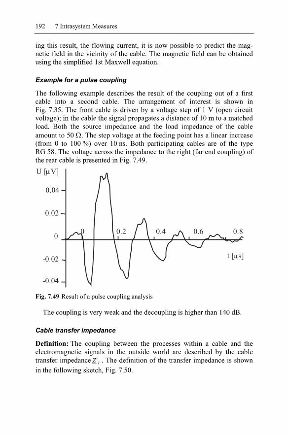
192 7 Intrasystem Measures
ing this result, the flowing current, it is now possible to predict the mag-netic field in the vicinity of the cable. The magnetic field can be obtained using the simplified 1st Maxwell equation.
Example for a pulse coupling
The following example describes the result of the coupling out of a first cable into a second cable. The arrangement of interest is shown in Fig. 7.35. The front cable is driven by a voltage step of 1 V (open circuit voltage); in the cable the signal propagates a distance of 10 m to a matched load. Both the source impedance and the load impedance of the cable amount to 50 Ω. The step voltage at the feeding point has a linear increase (from 0 to 100 %) over 10 ns. Both participating cables are of the type RG 58. The voltage across the impedance to the right (far end coupling) of the rear cable is presented in Fig. 7.49.
0 0.2 0.4 0.6 0.8
t [ s]μ
U [ V]μ
0.04
0.02
0
-0.02
-0.04
Fig. 7.49 Result of a pulse coupling analysis
The coupling is very weak and the decoupling is higher than 140 dB.
Cable transfer impedance
Definition: The coupling between the processes within a cable and the electromagnetic signals in the outside world are described by the cable transfer impedance TZ ' . The definition of the transfer impedance is shown in the following sketch, Fig. 7.50.

7.6 Cable coupling and cable transfer impedance 193
I
U
Ri
V
Z’T =UI
8
Fig. 7.50 Scheme showing the definition of the cable transfer impedance
TZ ' is a complex quantity and has the dimension Ω/m. TZ ' is a measure for the shielding efficiency of the cable screen, the smaller TZ ' the better the shielding efficiency. A more common definition reads:
( )lIdlUdZ T
1' = (7.115)
For the analysis of couplings in the frequency domain, only the magnitude of the cable transfer impedance is required. For the analysis of couplings in the time domain both the magnitude and the phase are required.
Cable transfer impedance of a homogeneous tube
The cable transfer impedance can be derived theoretically for a homoge-neous tube (Fig. 7.51), where the arrangement acts as replica of a full metal jacket cable (cable with a solid outer shield). The variation in trans-fer impedance with frequency for this arrangement, which often is used as reference, is presented in Fig. 7.52 for a copper tube of t = 0.1 mm thick-ness and an inner radius of 3 mm. The magnitude decreases exponentially; the phase is negative and decreases with increasing frequency. These trends are expected if it is recalled that the current will flow increasingly on a thin layer of the outer surface as frequency increases due to the skin effect. In addition, it should be recalled that the component of the current going into the metal (current density) is increasingly retarded with respect to the surface current as frequency increases. For a more theoretical treat-ment, the reader is directed to annex A6.1.
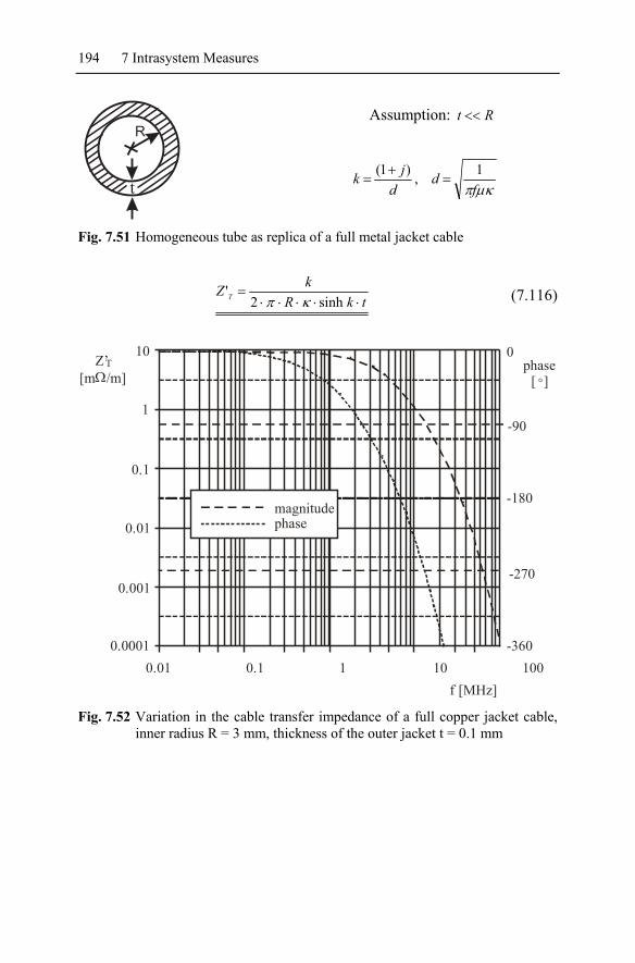
194 7 Intrasystem Measures
Assumption: Rt << R
t
μκπf
dd
jk 1,)1(=
+=
Fig. 7.51 Homogeneous tube as replica of a full metal jacket cable
tkRkZ T ⋅⋅⋅⋅⋅
=sinh2
'κπ
(7.116)
magnitudephase
f [MHz]0.01 0.1 1 10 100
10
1
0.1
0.01
0.001
0.0001
Z’[m /m]Ω
T phase [ ]°
0
-90
-180
-270
-360
Fig. 7.52 Variation in the cable transfer impedance of a full copper jacket cable,
inner radius R = 3 mm, thickness of the outer jacket t = 0.1 mm

7.6 Cable coupling and cable transfer impedance 195
R
r0
t
20
2n r
pR
⋅=
⋅
degree of perforation n = counts of holes per metre
Fig. 7.53 Model of a perforated tube
An Eq. (7.117) has been derived by Kaden [KAD59] for the prediction of a tube containing a large number of small holes (perforated tube). Only the influence of the holes is considered, the coupling through the material is neglected. The phase is positive and equals to 90°. When considering a real coaxial cable with a braided shield, the relation can only be used con-ditionally. However, one interesting result is given by the considerations of Kaden. It is shown again, that a large number of small holes are essentially better than a small number of larger holes, where the total hole area is taken as constant. The cable transfer impedance for the perforated cable is:
RrpjZ T
0023
2' ⋅⋅⋅
⋅= μω
π. (7.117)
From Eq. (7.117), a relation for calculating a hole inductance may be derived:
RrpL T
0023
2' ⋅⋅⋅
⋅= μ
π. (7.118)
Example 7.15: A hole radius r0 = 0.05 mm, together with an inner radius of the tube of R = 3 mm and a degree of perforation p = 0.417 mm/m, yields a hole inductance of LT’ = 0.6 nH/m.
Conversion: Cable transfer impedance into shielding efficiency
Comparing the equations for the cable transfer impedance of a full metal jacketed cable (7.116) and the shielding efficiency of a cylinder within a lateral magnetic field (7.45) reveals an interesting result. The comparision

196 7 Intrasystem Measures
shows that, given the condition 12>>
⋅⋅dR
rμ, a conversion between the ca-
ble transfer impedance TZ ' and the shielding efficiency sa is possible:
⎟⎟⎠
⎞⎜⎜⎝
⎛⋅
⋅⋅=
Ts Z
fa'
12
log20 0μ, (7.119)
.102
' 200sa
T
fZ−
⋅⋅
=μ
(7.120)
Transfer impedances of standard laboratory cables
The transfer impedance curves of a number of standard laboratory cables are presented with their magnitude and phase in Fig. 7.54. The curves were produced at the Dresden University of Technology.
Both the magnitude and the phase curves show very similar behaviour. Up to approximately 500 kHz the DC resistance of the braid and the phase have a constant value, where the phase is equal to 0°. Starting at approxi-mately 1 MHz, the magnitude increases by 20 dB/decade and the phase decreases to approximately -90°. Taking all uncertainties into considera-tion, it seems justifiable to calculate, to a first-order estimation, the cable transfer impedance using
mnHjmmZT /2/10' ω−Ω≈ . (7.121)
If the DC resistance per metre '0R of the braid is known, the following
approach for the cable transfer impedance can be used, leading in most cases to very sufficient results:
''0
' LjRZT ω−≈ , (7.122)
kHzRL
5002
'0'
⋅=
π. (7.123)

7.6 Cable coupling and cable transfer impedance 197
f [MHz]
f [MHz]0.01 0.1 1 10 100
0.01 0.1 1 10 100
Z’T
[ /m]
Phase
[ ]0
10
1
0.1
0.01
0.001
0
-30
-60
-90
-120
RG 59
RG 59
Fig. 7.54 Transfer impedances of standard laboratory cables
Remark: The use of this simplified procedure is only allowed for stan-dard laboratory cables, optimized and double optimized cables show a completely different behaviour. In Fig. 7.55 the course of such a cable is presented.

198 7 Intrasystem Measures
f [MHz]0.001 0.01 0.1 1 10 100
-150
-100
-50
0
50
100
150
Phase[Grad]
Z ‘T[ /m]Ω
f [MHz]0.001 0.01 0.1 1 10 100
0.0001
0.001
0.01
0.1
Fig. 7.55 Course of the transfer impedance of the cable RG 214 (measuring curve
of the Dresden University of Technology)
Exercises
Exercise 7.22: A twisted two wire cable has a core radius of rcore = 3 mm and a length of a turn of lturn = 20 cm. In the vicinity of the cable a homo-geneous magnetic field of 1 μT at 50 Hz is measured. How large will, un-der worst-case conditions, the voltage induced into the cable be?
Exercise 7.23: The situation presented in Fig. 7.56 is to be analysed by help of the program CONCEPT.
A twisted cable (radius of one wire rwire = 1 mm, insulation of the wires dIso = 0.1 mm) of 2 m in length is located in the vicinity of a rod antenna (starting at a distance of a = 2 m, running radially away from the antenna) with a height of h2 = 10 cm with respect to the ground. The twisted cable connects a symmetrical sensor (left hand side, output impedance of Zout = 100 Ω) with the differential input of a operational amplifier (right hand side, input impedance Zin = 100 kΩ). A power of 100 W at f = 3.5 MHz is radiated from the rod antenna (height h1 = 12 m, diameter of the rod d1 = 5 cm). A common mode suppression of 30 dB can be taken for the operational amplifier (conversion from a unsymmetrical signal into a symmetrical one).
a) How large is the interference voltage coupled into the signal circuit due to the radiation field of the antenna? For the substituting single wire a replacement radius of rsub = 2.2 mm should be chosen.
b) Vary the radius of the single replacement wire between 2.2 mm and 5 mm. How large is the maximum difference between the results (in dB)?
c) Which EMC-measure yields the highest immunity for the sensor-operational amplifier circuit?

7.6 Cable coupling and cable transfer impedance 199
d = 5 cm1h
= 1
2 m
1
h = 0.1 m2
2
a = 2 m
P = 100 W,f = 3.5 MHz
rad
= 2 mtwisted wire
Fig. 7.56 Analysis of the coupling into a symmetrical operating circuit
Exercise 7.24: A cylindrical single wire cable above ground has a self in-ductance per metre, which can be calculated by Eq. (7.83). As a good ap-proach, the resistance per metre of the cable shield can be estimated using either:
κπ ⋅⋅⋅=
trR
outer21'
0 (7.124)
for a cable having an outer conductor thickness t that is smaller than the skin depth d, or
κπ ⋅⋅⋅=
drR
outer21'
~ (7.125)
for a cable having an outer conductor thickness larger or equal to the skin depth. Calculate the frequency fG for which the inductance of the outer conductor is equal to the resistance, where router = 3 mm, t = 0.2 mm, height h = 5 cm above ground and the conductor material is copper.
Exercise 7.25: A current of I1 = 100 mA flows on the outer screen of a copper coaxial cable (router = 3 mm, t = 0.2 mm). What is the current that will be produced on a copper cable installed in parallel (router = 3 mm,

200 7 Intrasystem Measures
t = 0.2 mm, length of the parallel run l = 10 m, distance between both ca-bles d = 20 cm) at an operating frequency:
f1 = 100 Hz, f2 = 1 MHz?
Both cables have a height of h = 10 cm above ground. See Fig. 7.39.
Exercise 7.26: Within the conceptual phase of a frigate, there was a need to estimate the voltage UA coupled into a = 8 m long coaxial cable (router = 3 mm) at f = 5 MHz. The cable was intended to be installed at a height of h = 5 cm above ground. A magnetic field strength of H = 10 mA/m at 5 MHz was expected at the position of the cable.
Exercise 7.27: A signal current of I = 2 A at f = 3 MHz flows within a co-axial cable (length l = 5 m, outer radius router = 3 mm, height above ground h1 = 20 cm, both ends grounded). Estimate the magnetic field strength oc-curring under the coaxial cable (height h2 = 10 cm).
7.6.4 Cable shield connection at the device input
The system cabling requires a great amount of attention within the con-struction of a system, and with good reason. Cabling rules regarding each cable category and the installation distances are defined. The expected in-terference signals are then analysed by use of cable-matched transfer im-pedances. It is frequently overlooked in this stage of development, that an insufficient cable shield connection at the device input could invalidate the whole procedure.
Generally in this book, the connection of both ends of the cable screen to ground is assumed. Furthermore, the cable connection to ground is as-sumed to be implemented using a special cable gland, ensuring that the connection is around the whole area of the shield at the device input. A dif-ferentiation has to be made between a real cable shield (two or four con-ductors with a common shield or screen) and a coaxial cable (centre wire with a coaxial return conductor). In the coaxial cable the return conductor provides, at the same time, the shielding function of the cable.
Real coaxial cables have, for functional reasons, to be connected at both ends. It is most important to discuss, whether the outer conductor of a real coaxial cable may be connected to ground at its penetration point through a metallic wall. Problems may arise when leading a coaxial cable through the wall of a shielded room (EMC cabin) if very high decoupling values from the inner to the outer space have to be assured.
Not connecting the cable at the penetration point, which in some cases may prevent undesired interference signal transportation, should not be

7.6 Cable coupling and cable transfer impedance 201
considered as a good solution. Cables with optimized cable transfer im-pedance have to be used.
The quality of a cable shield connection is described by a lumped trans-fer impedance. The goal, which should be specified within cabling or de-sign guidelines, should be to achieve a transfer impedance of the cable shield connection that is equal to, or less than, the cable transfer imped-ance of a 1 metre cable that may be connected.
The transfer impedance of the cable shield grounding describes the ratio of the voltage Uinside, which occurs in the shielded area between the outer screen of the cable and ground, to the current Ishield, which is flowing from the cable screen to ground outside the shielded area. See Fig. 7.57.
II
shieldshield
k
inside
inside
U
UZ =
Fig. 7.57 Definition of the transfer impedance of a cable screen connection
The transfer impedance of the cable screen connection is a transfer quantity; it combines the outer current with the inner voltage. Conse-quently, an equivalent circuit of a current controlled voltage source can be created for the cable shield grounding (Fig. 7.58).
I
I
shieldconnect
shield
kinsideU Z Z =
Fig. 7.58 Equivalent circuit representing a cable shield grounding
The impedance of the shield connection Zconnect in the outer part of the circuit should not be confused with the transfer impedance Zk, which de-

202 7 Intrasystem Measures
scribes the coupling from the outer to the inner part. As with the cable transfer impedance, a direct equivalence between both quantities is given only for DC-currents. The transfer impedance of the cable shield ground-ing is, as with the cable transfer impedance, a function of frequency.
Different cable shield groundings with increasing effectiveness are shown in Fig. 7.59.
No grounding at the penetration point (a) The current is transported into the shielded area almost uninfluenced. The voltage of the cable screen to ground is almost the same both inside and outside the shielded area. The isolated penetration of a cable into the shielded area, and the inside connection of the screen to the electronic ground using a braid or pigtail, is completely forbidden.
insideU
Ishield
a)
no connection between cable screen and wall
insideU
Ishield
insideU
Ishield
insideU
Ishield
b)
pig-tail connection
c)
2 pig tails
d)
screw jont resp. welded
Fig. 7.59 Cable shield grounding with increasing effectiveness from a) to d)
Pigtail connection ( b) Regarding ground connections, a so-called a ‘pig-tail’-connection is where the shield or screen of the cable is removed shortly before entering the de-vice and the shield is connected to ground using a braid or a welded con-nection wire. The current has to flow either via the braid or the connecting
7.6 Cable coupling and cable transfer impedance 203
wire (pig-tail). The resulting current is concentrated and does not flow symmetrically in a 360° manner. An induction voltage occurs equal to
shieldconnectinside ILU ⋅⋅≈ ω (7.126)
where Lconnect is the self inductance of the circuit created by the connecting wire, a small piece of the cable shield and the shielding wall. For a first or-der approximation, this self inductance can be estimated using
Vm
connect RdlL ⋅
⋅⋅
=2ln
2πμ
, (7.127)
where: l = length of the connecting wire, RV = radius of the connecting wire, dm = averaged distance of the connecting wire to the cable shield and to the shielding wall.
Double pig-tail connection (c) The use of 2 connecting wires, installed completely symmetrically (same length, same distance, arranged opposite each other), will theoretically compensate for the inductive coupling. The current splits between the two connecting wires and the opposing orientation of the influenced areas with regard the excited magnetic field mean that the induced voltages on both sides compensate each other. This variation leads to a considerable im-provement compared to the use of only one connection wire. This would be sufficient in most cases to reach a low enough transfer impedance, and with it a sufficient compensation, if the symmetry could be realised and maintained in reality.
The use of 4 (8, 16, 32.....) connecting wires, located symmetrically on the perimeter, increasingly improves the situation, especially under real field conditions. Nevertheless, the complete field compensation will not be reached within real installations. The inductive coupling cannot be reduced to very small values until a fully coaxial connection over 360° is used.
Screwing, welding (d) Optimal decoupling is achieved using a circumferential welding. However, this solution has the drawback that the heat required could destroy the in-sulation. Furthermore, a cable welded into a wall cannot be replaced with-out damaging the wall. Further solutions are available on the market in or-der to get very good cable shield grounding. For further details, the reader is directed to the reference [VG994].

204 7 Intrasystem Measures
1 shielding wall2 cable with dismantled screen3 saddle shaped bulge4 metal granules, f. i. copper 5,6 filling openings7 emptying opening8,9 strain relief10,11 dust covers12 fixing srews
Fig. 7.60 Highly efficient cable shield grounding
A commercially available cable shield grounding box, which fulfils very high requirements is presented in Fig. 7.60. The measured values of the transfer impedance are shown in Fig. 7.61.
0.01 0.1 1 10 100 1000
f [MHz]
Zk
[dB ]
0
-20
-40
-60
-80
-100
-120
cable shield connection, circumferentially
connection according to Fig. 7.60
Fig. 7.61 Plot of the transfer impedance of the cable shield grounding of Fig. 7.60

8 Atmospheric Noise, Electromagnetic Environment and Limit Values
Every electrical or electronic device or system has to fulfil emission limit values and has to show a predefined immunity against impinging disturb-ing signals. The rationale for requiring a predefined immunity is as fol-lows: An electrical/electronic device should fulfil its function satisfactorily if interferences signals are impinging on it from the outer world; at the very least, it must not be destroyed. The signals from the outer world are, in general, not to be influenced and therefore must be considered as given.
Interference signals affecting a device can be roughly categorised into the following:
• Impinging of permanently acting signals • Pulse shaped singularly occurring or multiple signals
The permanently acting signals comprise, for instance, the signals of li-censed radio stations, low frequency magnetic fields of power appliances and harmonics from rectifier circuits or non-linear loads on power sup-plies. The immunity against permanently acting signals must be suffi-ciently high that the operation of the device is undisturbed during the inter-ference.
The pulse shaped signals comprise, for instance, an electrostatic dis-charge (ESD); the multiple, rapid, low energy pulses (bursts, from for in-stance switching inductors), as well as the high energy one-time signals from a distant lightning strike and signals from switching actions within the power supply (surges). The individual immunity against pulse shaped signals is dependent on the task and the operating environment of the de-vice. The result of interference is differentiated into
• interferences that only occur temporarily during the impact of the in-terference signal (for instance during an ESD),
• disturbances that are eliminated by a automatic self re-start of the device (for instance, after the impact of a burst),
• disturbances that require human intervention (for instance, after the impact of a surge).
K.-H. Gonschorek, R. Vick, Electromagnetic Compatibility for Device Design and System Integration, DOI 10.1007/978-3-642-03290-5_8, © Springer-Verlag Berlin Heidelberg 2009

206 8 Atmospheric Noise, Electromagnetic Environment and Limit Values
8.1 Atmospheric noise sources, electromagnetic environment
It is simple to justify the requirement that interference emission limit val-ues must be met: for the protection of the general public. However, it is more difficult to explain how the limit values themselves are set. The al-lowed magnitude of interference emissions is derived from the required mutual compatibility of devices fixed in the definition of EMC: “…..without disturbing the environment, which also comprises other ap-pliances, in a disallowed manner!”
When does a disallowed interference occur? Which interference victims have to be considered?
Restricting ourselves to the frequency range above 10 kHz, the answer is found very quickly: The most sensitive interference victims are commu-nication receivers with their antennas. It is the task of these devices to pick up information at their accepted frequencies, then to evaluate and prepare the information for the user. This task is performed up to the physical limit of the system. If this operational requirement is to be fulfilled, the follow-ing condition is given:
An electrical/electronic appliance is not allowed to produce an inter-ference signal, which is higher than a wanted signal evaluable by the receiving system, at the position of an antenna.
In fulfilling the above statement, defining a minimum distance between an electrical/electronic device and a receiving antenna, reduces the prob-lem to the question: what is the minimum signal that can be evaluated by the system?
Two limits are given:
1. the unalterable atmospheric noise of natural noise sources,
2. the noise of the receiver itself, which is normally considerably lower than the atmospheric noise, received and converted by the antenna to the receiver input.
These quantities define the way for fixing the emission limit values in the frequency range above 10 kHz. Probability and bandwidth considera-tions, as detailed problems, are not discussed here. However, reference to the CISPR 16 standard [CIS92] is made for completeness.
8.1 Atmospheric noise sources, electromagnetic environment 207
In order to accurately record the interference potential of an electri-cal/electronic appliance, with respect to disturbing communication recep-tion, the frequency range is divided into two ranges.
Frequency range up to 30 MHz (λ ≥ 10 m)
Within this range the connecting cables mainly act as antennas, which emit the interference signals produced by the EUT into the environment. On the other hand, transmission lines have the ability to be selective with relation to frequency. Since it is impossible to test the emission with all transmis-sion line lengths used in its future application, it is necessary to use a sub-stitute. This substitute consists of a substituting impedance called LISN (LISN = line impedance stabilization network). An interference voltage measurement (source measurement) is carried out using a LISN. The limit values for the interference voltage are chosen in such a way that, by excit-ing a matched λ/2-dipole by this voltage at each frequency, a field strength is produced that does not lead to a disturbance (or a disallowed interfer-ence).
Frequency range above 30 MHz (λ< 10 m)
With increasing frequency the EUT with its components, its openings and its cabling become more and more like a radiator. This leads to the reality that, measurements performed solely on cables (power cables) do not suf-ficiently characterise the interference potential of the EUT. Therefore, measurements of the field strength are carried out in this frequency range.
Nevertheless, the starting point for the definition of the limit values re-mains the unalterable noise of the natural noise sources. This noise is mainly produced by discharges of static electricity in the atmosphere (lightning strikes from the clouds to the earth and between clouds). In this context the effects, which occur in the form of impulses at great distances, rather than the nearby actions are considered.
It can be assumed that approximately 1000 lightning strikes per second occur on the whole of Earth. Furthermore, assuming that the model of trav-elling waves within the lightning channels is several kilometres long, it be-comes clear that the high-frequency components of the radiated field be-have like electromagnetic communication waves. Reflections occur on the ionized layers of the ionosphere. Hence, lightning discharges in the vicin-ity of the equator can be considered as impulse interferences in Europe. To that end, the unchangeable environmental noise at a certain place on Earth is dependent on the position, on the time and also on the season. State-ments made in this direction should always be treated statistically. It is in-

208 8 Atmospheric Noise, Electromagnetic Environment and Limit Values
teresting to demonstrate, that performing a measurement of the outside noise using a directional antenna shows a maximum reading if the antenna is pointing towards the equator. This verifies that the highest number of lightning strikes occur in this region.
In order to have an appropriate degree of confirmed data for the plan-ning of communication plants, for fixing the radius of possible radio com-munications and for deriving interference emission limit values, the Inter-national Telecommunication Union (ITU) has issued report 322 [ITU64], ‘World distribution and characteristics of atmospheric radio noise’. This report contains the atmospheric noise for every position on earth for all 4 seasons and for 6 different periods of the day. Of special interest is the first sentence of the introduction, which reads: ‘The determination of the mini-mum signal level for satisfactory radio reception in the absence of other unwanted radio signals necessitates a knowledge of the noise with which the wanted signal must compete’.
Fig. 8.1 Expectation value of the atmospheric noise Fam in
0kT bdB , spring time, 08.00 – 12.00 GMT
Unfortunately the report is not easy to read, because the presented dia-grams are intended for planning engineers and the operators of radio and telecommunication plants. In addition to absolute values, information

8.1 Atmospheric noise sources, electromagnetic environment 209
about the probability of occurrence is delivered. Furthermore, the whole frequency range from 10 kHz to 100 MHz is covered.
One diagram for the atmospheric noise (noise power) Fam as dB-values related to k⋅T0⋅b (k = Boltzman constant, T0 = absolute tempera-ture = 293 K = 20° C, b = bandwidth = 1 Hz), for a frequency of f = 1 MHz, is presented in Fig. 8.1. The diagram is valid for spring time during the time period of 08.00 - 12.00 GMT. A value of 27
0kT bdB can be found for Dresden (Germany).
In order to calculate the noise amplitude at other frequencies, another diagram has to be used. A diagram showing the curves of frequency de-pendency is repeated in a simplified manner in Fig. 8.2. The curve that should be used is the curve containing, at f = 1 MHz, the value taken from Fig. 8.1 (for our case 27).
F [
dB
]
amkT
b 0
180
160
140
120
100
80
60
40
20
0
-20
0.01 0.1 1 10 100 f [MHz]
Galactics noise
0
1 3 5 1 3 5 1 3 5 1 3 5
20
30
60
80
Fig. 8.2 Frequency dependency of the atmospheric noise Fam in
0kT bdB , spring time, 08.00 – 12.00 GMT
Generating the curve (Fam = f(f)) for a specific location (Dresden), sea-son and period of the day allows a conversion into the real noise field strength En. The conversion equation required is:
mVkHzMHzamn dBbfFE /log10log205.65 μ⋅+⋅+−= , (8.1)

210 8 Atmospheric Noise, Electromagnetic Environment and Limit Values
fMHz = frequency of interest in MHz, bkHz = bandwidth of the measuring equipment in kHz.
Remark: In this equation, En (instantaneous value) is combined with Fam (mean value) for the presented time period, which is acceptable with re-spect to the philosophy of creating emission limit values.
The result of corresponding evaluations and calculations are presented in Fig. 8.3. The curves for the following periods are presented:
Spring time, 08.00 - 12.00 GMT (lowest values) Autumn time, 04.00 - 08.00 GMT (medium values) Summer time, 20.00 - 24.00 GMT (highest values)
0.01 0.1 1 10 100 1000Frequency [MHz]
-40
-30
-20
-10
0
10
20
30
40
50
60
70Dresden
spring time 8 - 12 summer time 20 - 24autumn time 4 - 8
“Man-made-noise”city regionsuburbia regionmore rural region
atmospheric noise
μV/m
Elec
tic fi
eld
stre
ngth
[dB
]fo
r a m
easu
ring
band
wid
th o
f 10
kHz
Galactic noise
Fig. 8.3 Noise from atmospheric discharges, man-made noise and noise traced
back to sources in outer space, for a measuring bandwidth of 10 kHz
Curves for man made noise and galactic noises are also shown in this diagram. It should be noted that these curves are only medium value curves, containing sizeable statistical uncertainties. Nevertheless, they are valuable when used for planning reasons. The man made noise represents the pulse interference produced by:
• a superposition of all switching actions, • corona discharges,
8.1 Atmospheric noise sources, electromagnetic environment 211
• imperfect contacts of rail pantographs, • chatter during switching actions of electric power.
The low antenna efficiency of the noise sources lead to large differences between interferences in the city, suburban environments and rural regions. The galactic noise is a result of signals from outer space that originate from the physical processes in material transmutations at very great dis-tances.
In order to obtain the field strength from the values of Fam according to Eq. (8.1), some prerequisites have to be mentioned and some conversions have to be performed. The report 322 contains all necessary information to enable the reader to carry out this conversion, but only in an indirect man-ner.
Eq. (8.1) is explained in a more detail in the following chapter, both for completeness and to provide an understanding for a developing engineer or a manufacturer. This explanation aids in applying limit values as their ba-sis is understood.
Fam defines the time mean value of the quantity Fa over a considered time slot of 4 hours. Fa is defined as the noise power Pn specified in dB with relation to k⋅T0⋅b (293 K, 1 Hz), where Pn is given by the following expression:
AEPn ⋅=Γ
2
(8.2)
E = electric field strength, A = effective antenna area, Γ= 377 Ω.
From this it follows
bTkPbTk
PF ono
na log10log10log10log10 ⋅−⋅⋅−⋅=
⋅⋅⋅= . (8.3)
Using Eq. (8.2), the noise power can be expressed as
ΓAEP
nE
n log10log20log10 ⋅+⋅=⋅ . (8.4)
The intermediate step of
bTkFAE oan log10log10log10 ⋅+⋅⋅+=⋅+Γ , (8.5)
leads to

212 8 Atmospheric Noise, Electromagnetic Environment and Limit Values
[ ]Ωπ
λ37716
3log10log10302042
/ ⋅⋅⋅
⋅−++−= kHzbdBdBFE HzJan . (8.6)
In this equation the following relations have been used:
KTdBdB HzJTk 293,2040 0/0=−=⋅ , (8.7)
πλ⋅
⋅=
163 2
A for a short antenna above a conducting plane, (8.8)
[ ] [ ]kHzbdBHzb log1030log10 ⋅+= . (8.9)
Furthermore, using
[ ]
2
m/s
310 log 38 dB 20 log16 377
38 dB 49,5dB 20log f MHz
Ω
Ω
⋅λ− ⋅ = − ⋅ λ
⋅π⋅ Ω= − +
(8.10)
yields the final relation:
mVkHzMHz
smHzJan
dBbfdBdBdBdBFE
/
//
log10log205,493830204
⋅+⋅
+−++−= Ω. (8.11)
Remark: In deriving the noise field strength the effective antenna area has been used. The effective antenna area defines the area, which, multi-plied by the radiation power at the location of the antenna, yields the maximum power to be fed into a matched receiver. See chapter 5.3. With this relation, a quantity En (electric field strength) is given, which allows the prediction of the noise power PR for an arbitrary antenna in a simple way. If the effective area Aw of this antenna is given the following expres-sion can be used:
wn
R AEP ⋅=Γ
2
. (8.12)
It can be seen from the diagram of Fig. 8.3 that the differences between the lowest and the highest noise value can reach values of up to 50 dB. Therefore, a decision must be made as to which value should be taken. It is not reasonable to choose the lowest noise values as basis for the definition
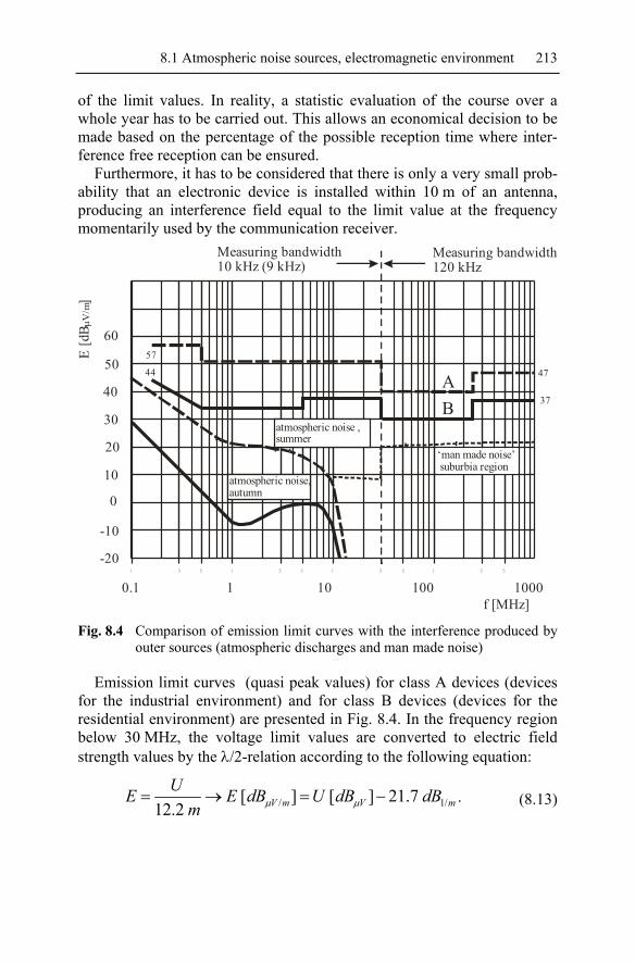
8.1 Atmospheric noise sources, electromagnetic environment 213
of the limit values. In reality, a statistic evaluation of the course over a whole year has to be carried out. This allows an economical decision to be made based on the percentage of the possible reception time where inter-ference free reception can be ensured.
Furthermore, it has to be considered that there is only a very small prob-ability that an electronic device is installed within 10 m of an antenna, producing an interference field equal to the limit value at the frequency momentarily used by the communication receiver.
1 3 5 1 3 5 1 3 5 1 3 5
f [MHz]0.1 1 10 100 1000
E [d
B
]
μV/m
-20
-10
0
20
50
60
30
40
10
57
44 47
37AB
‘man made noise’ suburbia region
atmospheric noise ,summer
atmospheric noise,autumn
Measuring bandwidth10 kHz (9 kHz)
Measuring bandwidth120 kHz
Fig. 8.4 Comparison of emission limit curves with the interference produced by
outer sources (atmospheric discharges and man made noise)
Emission limit curves (quasi peak values) for class A devices (devices for the industrial environment) and for class B devices (devices for the residential environment) are presented in Fig. 8.4. In the frequency region below 30 MHz, the voltage limit values are converted to electric field strength values by the λ/2-relation according to the following equation:
/ 1/[ ] [ ] 21.712.2 V m V m
UE E dB U dB dBm μ μ= → = − . (8.13)
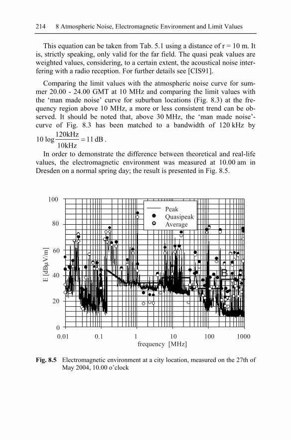
214 8 Atmospheric Noise, Electromagnetic Environment and Limit Values
This equation can be taken from Tab. 5.1 using a distance of r = 10 m. It is, strictly speaking, only valid for the far field. The quasi peak values are weighted values, considering, to a certain extent, the acoustical noise inter-fering with a radio reception. For further details see [CIS91].
Comparing the limit values with the atmospheric noise curve for sum-mer 20.00 - 24.00 GMT at 10 MHz and comparing the limit values with the ‘man made noise’ curve for suburban locations (Fig. 8.3) at the fre-quency region above 10 MHz, a more or less consistent trend can be ob-served. It should be noted that, above 30 MHz, the ‘man made noise’-curve of Fig. 8.3 has been matched to a bandwidth of 120 kHz by
120kHz10 log 11 dB
10kHz= .
In order to demonstrate the difference between theoretical and real-life values, the electromagnetic environment was measured at 10.00 am in Dresden on a normal spring day; the result is presented in Fig. 8.5.
PeakQuasipeakAverage
100
80
60
40
20
00.01 0.1 1 10 100 1000 frequency [MHz]
E [d
BV
/m]
μ
Fig. 8.5 Electromagnetic environment at a city location, measured on the 27th of
May 2004, 10.00 o’clock

8.1 Atmospheric noise sources, electromagnetic environment 215
The curve was produced using an EMI-receiver (CISPR-receiver) in the operation mode: ‘quasi peak’. In this operation mode, the measuring bandwidth for each frequency range is automatically chosen. Up to 150 kHz a measuring bandwidth of 200 Hz is chosen, from 150 kHz up to 30 MHz a measuring bandwidth of 9 kHz is chosen, and above 30 MHz a bandwidth of 120 kHz is chosen by the receiver. The active E-field-antenna Schwarzbeck EFS 9219 was used for the frequency range from 10 kHz to 30 MHz. In the range from 30 MHz to 300 MHz a biconical an-tenna was used. Finally, above 300 MHz a log-periodic antenna was used. The average and peak values are also presented in this diagram. In the higher frequency range an insufficient resting time can be recognized in measuring the peak values. Furthermore, it has to be considered that the values are not precisely taken at the same time.
The curve of limit class B (residential environment) is also plotted in Fig. 8.5. The following can be detected:
1. There exist frequency ranges where the outer noise (atmospheric noise, man made noise) impact stays below the limit line.
2. There are signals above the limit values in very large regions of the frequency spectrum.
The second statement, which leads only to a restriction in the use of OATS (open air test sites), will not be covered in detail at this point.
The first statement, if it is not considered relatively, should be regarded tentatively. In the frequency ranges where the outer noise is lower than the limit value, it can be shown that there is the possibility that received sig-nals can be evaluated providing no disturbance from an electronic device is present. It can often be difficult to demonstrate to an inexperienced user, unfamiliar with this problematic nature, that an electronic device can stay within the legal limit values but still produce disturbances.

216 8 Atmospheric Noise, Electromagnetic Environment and Limit Values
1 3 5 1 3 5 1 3 5 1 3 5
f [MHz]0.1 1 10 100 1000
E [d
B
]
μV/m
0
10
20
50
60
70
80
30
40
57
44 47
37
AB
174 - 285 kHz
525 - 1600 kHz
41 - 68 MHz87.5 - 104 MHz
174 - 230 MHz
470 - 790 MHz
VG 95 373 T22Limit value class 1
Measuring bandwidth120 kHz
Measuring bandwidth10 kHz (9 kHz)
Fig. 8.6 Comparison of minimum field strength values, for an interference free
reception [GO/SI92] of public radio stations (VDE 0855 T1), with the limit values for radiated signals. Up to 30 MHz the limit values relate to the magnetic component (converted to electric field strength using a free space impedance of 377 Ω). The VG-limit values (military devices) are converted to those at a measuring distance of 10 m using a 1/r-law.
In order to avoid unnecessary problems and to provide a certain degree of confidence in a system, minimum field strength values have been de-fined, which must be present at the position of an antenna in order to achieve undisturbed signal reception.
A comparison between these minimum field strength values and the CSPR-limit classes A and B together with limit class 1 of VG 95 373 T22 (VG = Verteidigungsgeräte = military devices), is shown in Fig. 8.6. Whilst evaluating these comparisons, it has to be considered that a certain signal to noise ratio (S/N-ratio) must be satisfied so that the received signal can be evaluated.
The most essential points to consider regarding radio interference are:
• An outer noise exists that cannot be influenced.

8.1 Atmospheric noise sources, electromagnetic environment 217
• Human beings themselves produce a noise spectrum through usage of electric energy.
• An electrical/electronic device is only allowed to produce a speci-fied interference field strength at a defined distance.
• Taking the necessary S/N-ratio into consideration, which is depend-ent on the radio service being considered, the minimum field strength values can be calculated that must be satisfied to guarantee a high probability of interference free reception.
Exercises
Exercise 8.1: A FM-car radio operates using a rod-antenna with a length of 0.4 m (electrical length: 0.2 m). Due to insufficient matching of the an-tenna to the receiver, coupling losses of approximately 6 dB occur. The re-ceiver sensitivity amounts to -122 dBm for a bandwidth of 120 kHz. The signal to be received has, at the position of the car, an electric component of V
m100 μ . The outer noise per kHz amounts to Vm kHz
12 dB μ⋅
. How large is
the signal to noise ratio S/Ntotal (considering the total noise) at the input of the receiver?
Exercise 8.2: A mobile phone receiver has a 25 kHz-sensitivity of -120 dBm at 40 MHz (self noise of the receiver). The 2 m-rod antenna cre-ates an effective antenna area of 6.7 m2. In times of high sunspot activity the interference radiation of the sun at f = 40 MHz amounts to
2m
m kHz
I 127 dB= − . Under these conditions the desired signal to be received is
ENeff = Vm3 μ .
a) How large is the signal to noise ratio (S/N ratio) at the receiver input, not considering the sun interference?
a) How large is the ratio of wanted signal to interference signal of the sun?
b) Do you think that the reception of a wanted signal suffering low-interference (S/N > 20 dB) is possible?
Exercise 8.3: In the ITU-report, an averaged outer noise power of Fam = 42
0kT bdB at f = 10 MHz is stated for Dresden during the winter time
and a period from 20.00 – 24.00 GMT. a) How large is the noise field strength En for a bandwidth of 25 kHz?

218 8 Atmospheric Noise, Electromagnetic Environment and Limit Values
b) A receiver is operated on a Yagi-antenna with a gain of Gi = 8 dB (gain with relation to the isotropically radiating antenna). How large is the noise voltage at the input of the receiver (open circuit voltage)?
8.2 Conversion of limit values
8.2.1 Distance conversion
Electrical and electronic devices have, among other things, to fulfil the limit values of radiated electromagnetic interference signals. A manufac-turer of an electrical device can justifiable expect that the defined measur-ing method is indisputable so that, arranging and operating the device ac-cording to the suitable standard, ensures that the device will pass the EMC test. A manufacturer can be sure of this results assuming: the arrangement was varied in a responsible way, the installation was fixed to produce the highest interference emissions and the operation mode was used, and set, that delivered the highest emissions.
Furthermore, the manufacturer (or his test laboratory) can undersign the manufacturer declaration of conformity with confidence, and assume that they have done a responsible job, providing that the DUT (device under test) has been turned and the maximum interference emission located using an amplitude scan in the frequency range from 30 MHz to 1 GHz.
These methods for measuring the radiated interference emissions are straightforward in terms of civilian applications. The compliance of the emission values to the limits will be tested at a distance of 10 m from the DUT (equipment class B), which can be reasonably performed only in an anechoic chamber.
A fee of approximately 1,000 Euro is common for a one test day in an anechoic chamber large enough for the DUT and allowing a measuring distance of 10 m; additional costs for setting-up equipment and for writing the report have to be added (fee approximate for 2007). For electrical (electronic) products produced in large numbers, such expenses are justifi-able. However, it is reasonable to ask in terms of the profit, what is the economical benefit for a low volume production or for a unique specimen.
On the other hand, the manufacturer has to make sure that there is a high probability that his device fulfils the emission limit values. This can also be performed as part of an arrangement that does not completely satisfy the standards. Often the measurements are carried out at a smaller distance than defined in the standard (due to space restrictions or to improve the ability to discriminate between emissions from the DUT and signals com-
8.2 Conversion of limit values 219
ing from the environment). Hence, it must be discussed how to convert the values measured at a distance rM to the distance rN defined in the used stan-dard.
Three possibilities are given.
1. Up to π2
00
crf N ⋅= the conversion is done using
3
⎟⎟⎠
⎞⎜⎜⎝
⎛
N
M
rr ,
3
⎟⎟⎠
⎞⎜⎜⎝
⎛⋅=
N
MMN r
rEE , (8.14)
Starting with f0 the conversion is done using ⎟⎟⎠
⎞⎜⎜⎝
⎛
N
M
rr ,
⎟⎟⎠
⎞⎜⎜⎝
⎛⋅=
N
MMN r
rEE . (8.15)
These conversions are derived by considering the DUT as an elemen-tary dipole where the transition region is neglected.
2. For the whole frequency range, the conversion is carried out using
⎟⎟⎠
⎞⎜⎜⎝
⎛⋅=
N
MMN r
rEE .
The field strength estimated using this expression is too high in the lower frequency range, up to f = f0, if the DUT is acting like an ele-mentary dipole. According to EN 61000-6-4:2001, for the industrial environment, it is generally permitted that measurements are carried out at a distance of 10 m and the limit values are modified by a re-duction of 10 dB.
3. In the whole frequency range the value EM measured at the smaller distance is used for the comparison with the limit value:
MN EE = .
This possibility is allowed according to the standards. It normally leads to an over testing of the DUT. However, the rationale is easy to understand. An extended DUT will, with increasing frequency, in-creasingly show the behaviour of an aperture antenna. For an aper-ture antenna, the transition from the Fresnel zone (beam forming re-gion) to the Fraunhofer zone (E ~ 1/r) can be approximated by

220 8 Atmospheric Noise, Electromagnetic Environment and Limit Values
λ
22 DrF
⋅= (8.16)
(D = diagonal of the antenna area, λ = wavelength). Starting from rF, the required 1/r-dependency is given. Up to rF, various dependencies up to E = constant are possible, depending on the antenna type. Tak-ing, for instance, a switching board with a diagonal dimension of 2.3 m as the DUT; a transition distance of rF = 35 m is calculated for a wavelength of 30 cm (f = 1 GHz).
Result: Measurement at a smaller distance than the distance in the standard is possible. However, the measuring value has to be compared with the limit value of the standardised distance.
Alternative: Understandable statements for a decrease of the field are given within the test report.
8.2.2 Conversion E H and H E
The procedure for checking the radiated interference emission in the mili-tary region differs considerably from that of the approach for civilian ap-plications. Consequently, both in the German VG-standards and the American MIL-standards (MIL-STD = military standard), the radiated in-terference emission limits are validated at a distance of 1 m (measured from the surface of the device).
According to the American regulations (MIL-STD-461 (E)), the electric field starting at 14 kHz is measured. The VG standards require the compli-ance of the radiated interference limit values for the magnetic field starting at 10 kHz. If, for instance, a complex system (frigate, submarine, tank, sat-ellite) is built according to the VG standards, the question has to be asked: does equipment qualified according to the MIL-STD have to be tested again, or, how does this situation have to be assessed and how can the measured values be converted? In addition, the reverse situation applies where devices qualified to VG have to be integrated into a system built ac-cording to MIL-STD.
In the higher frequency range, starting at 01
1 m cf 48 MHz
2⋅
= =π
(from
the dipole relations), conversions between E → H or H → E can be per-formed with help of the free space wave impedance:
V/ m A / m V / AE[dB ] H[dB ] 51.5 dBμ μ
= + . (8.17)
8.2 Conversion of limit values 221
It is no longer permissible to assume a constant wave impedance be-tween the E-field and the H-field in the frequency range below f1. A first order approximation is gained by assuming behaviour like that of the ele-mentary dipoles.
Conversion E H
In the following discussions, a situation is evaluated in which a device measured according to MIL-STD has to be evaluated to VG. To provide a ‘worst-case’ approximation it is implied that:
a) The field is produced by a magnetic source, which can be described by a pure magnetic dipole.
b) The E-field (E0) is measured by an E-field-antenna at a distance of 1 m from the surface for the DUT.
The following calculations can be performed:
1. Below 48 MHz, the wave impedance of the field of a magnetic sour-ce at a distance of 1 m from the source is given by
7.9 [ ]M f MHzΓ = ⋅ Ω . (8.18)
2. Hence, the magnetic field strength H0 is calculated by
A/m][9.7
]/[000 MHzf
mVEEH
M ⋅=
Γ= . (8.19)
3. The limit values for the magnetic field are normally specified with dimensions [V/m]. The real, measured magnetic field H is trans-ferred into these units by multiplication with 377 Ω. If the electric field strength converted from the magnetic field is denoted by EV, the following relation is given:
Ω377⋅= HEV , (8.20)
consequently, if the measuring distance is 1 m, the relation reads EV0 = H0⋅377 Ω.
4. A magnetic field measured at a distance of 1 m corresponds to a converted electric field of
[ ]0 0
48VE E
f MHz= , (8.21)

222 8 Atmospheric Noise, Electromagnetic Environment and Limit Values
])[log(206.33][][ /0/ MHzfdBdBEdBE MHzmVmVVO −+= μμ . (8.22)
This value has to be compared with the limit curve for the magnetic field at a distance of 1 m.
5. These relations are valid up to f = 48 MHz for the considered meas-uring distance.
Example 8.1: An electric field strength of E0 = 50 µV/m (= 34 dBµV/m) from a magnetic source has been measured at f = 50 kHz. According to Eq. (8.22), this results in a converted magnetic field of EV0 = 48 mV/m (= 94 dBµV/m). If this value is compared with the limit value of SA02G, a limit overshoot of 24 dB is calculated. If no conversion according to the procedure above had been carried out, the device would meet the limit value with a positive margin of 36 dB.
Example 8.2: An electric field strength of E0 = 10 µV/m (= 20 dBµV/m) from a magnetic source has been measured at f = 14 kHz. According to Eq. (8.21), this results in a converted magnetic field of EV0 = 34.3 mV/m (= 91 dBµV/m). Now a limit value overshoot of 8 dB is calculated according to SA02G.
Conclusion: Assuming that the DUT is a pure magnetic source and that the limit values RE02 of MIL-STD are fulfilled, or only slightly exceeded, considerable limit overshoots may be given with relation to the VG limit values of SA02G.
Conversion H E
Considering now a situation in which an electric source has been measured using a magnetic antenna, the same relations apply, only with a reverse sign. A magnetic field strength (H0) is measured using a magnetic antenna (loop antenna) that amounts to Ev0 = H0⋅377 Ω. In this case, the following can be derived:
1. Below 48 MHz, the wave impedance of an electric source at a dis-tance of 1 m from the source is given by
[ ] ΩΓMHzfE
18096= . (8.23)
2. Using this wave impedance yields a real field strength of

8.2 Conversion of limit values 223
[ ]0 V 0
48E E
f MHz= , (8.24)
])[log(206.33][][ /0/0 MHzfdBdBEdBE MHzmVVmV −+= μμ . (8.25)
This field strength E0 has to be compared with the corresponding limit value.
Example 8.3: A magnetic field strength from an electric source of EV0 = H0⋅377 Ω = 1 mV/m (= 60 dBμV/m) has been measured at f = 200 kHz. According to Eq. (8.24), a real electric field strength of E0 = 0.24 V/m (= 108 dBμV/m) is calculable.
Conclusion: Under the prevailing condition that the interference source is an electrical one and that the VG limit values SA02G are met, or only exceeded slightly, considerable limit overshoots may be given with regard the MIL-STD limits RE02.
Exercises
Exercise 8.4: The following field strength values of a DUT have been measured at a distance of rM = 3 m from its surface:
a) f = 30 MHz → EM = 60 dBμV/m, b) f = 100 MHz → EM = 50 dBμV/m, c) f = 1 GHz → EM = 40 dBμV/m.
The DUT consists of a 19“-housing with a power cord and external sen-sor (1 m cable to the sensor). Which value should be chosen at a measuring distance of rN = 10 m to compare with the limit values? Explain your choice.
Exercise 8.5: An electric field strength of E0 = 47 dBµV/m, at a distance of r = 1 m and a frequency of f = 14 kHz, has been measured in front of the screen of a monitor (electric source). What value is calculated for the con-verted magnetic field strength (EV0 = H0⋅377 Ω) if the dipole relations are used?

224 8 Atmospheric Noise, Electromagnetic Environment and Limit Values
Exercise 8.6: An electric field strength of E0 = 38 dBµV/m has been meas-ured from a magnetic interference source at a distance of 1 m and a fre-quency of f = 80 kHz.
a) How large is the magnetic field strength H0 in dB µA/m at the measur-ing point?
b) How large is the magnetic field strength converted into an electric field strength?
c) Recalculate your answers to questions a) and b) for the case where the field of an electric interference source has been measured.

9 EMC Engineering and Analysis
“Only the systematic engineering, called EMC-planning, during the entire procedure of establishing a complex system ensures the EMC of a system during its utilization phase.”
This sentence introduces the chapter, ‘phases and phase papers of an EMC-planning’, in [GO/SI92]. The validity of this sentence is undisputa-ble still today. Moreover, the necessity of an EMC-planning has increased. The procedure described in the cited chapter, relating strongly to the VG-methodology, guaranties that in any case a coherent, logical and continu-ous EMC-planning is carried out.
The essential parts of these statements are repeated, extended and up-dated in this chapter, whilst not making regular reference to the aforemen-tioned literature.
The extent of EMC-system planning required depends on the complex-ity of the system to be constructed. The procedures described herein appeal primarily to the system planner. These are a maximum requirement that have to be reduced by an EMC working group (EMCAB = EMC advisory board) or the person responsible for the EMC.
By considering the manufacturing process of an electrical/electronic de-vice, it has proven valuable to also recognise and execute an EMC equip-ment planning matched to the complexity of the device. The depth of plan-ning depends on the complexity of the equipment under construction; more so for a device than for a system. Take for example a control station of a power plant; it becomes immediately clear that without a very detailed EMC-planning, with appropriate documentation, nothing meaningful is possible.
At the start of a device development the following should be fixed:
• What EMC-environment the device is to be developed for
• From this, which EMC-standards have to be considered and which EMC-limit values have to be fulfilled
• The construction of the housing (metal, metallised plastic, or no shielding)
K.-H. Gonschorek, R. Vick, Electromagnetic Compatibility for Device Design and System Integration, DOI 10.1007/978-3-642-03290-5_9, © Springer-Verlag Berlin Heidelberg 2009

226 9 EMC Engineering and Analysis
• The kind of power supply
• The kind of peripheral equipment to be connected, and it what way
• Particular requirements with respect to the immunity
• The failure criteria if external disturbance signals are impinging
• The EMC-experiences from similar former projects
• The specifications of the internal cabling and wiring and the ground-ing philosophy to be followed
• How signal interfaces (input and output) have to be installed in a de-fined area of the device surface (single-point entree) and, moreover, specifying their position
• Which EMC-tests have to be carried out during the construction of the device
Subsequently, in the sense of this chapter, an EMC-planning at the de-vice level (for the conceptual phase) has been executed. Adhering to the guidelines, and possibly updating them, reduces the EMC-test for confirm-ing the manufacturer’s declaration of conformity to a formal act.
All considerations, measures and decisions regarding EMC are written down during the entire development process of a project. This produces a clarity that allows for simple retrofitting in the case of incompatibilities and limit overshoots. Furthermore, the assignment of guilt at a later date is avoided to some extent.
The tasks within the EMC-planning and EMC-management of a com-plex system consist of:
1. Collection of data relevant for the EMC, including • Proposed purpose and location • Constructional facts • Devices to be installed
2. Subdivision of the system into EMC-zones utilizing natural borders (mechanical shielding walls)
3. Specification of limit values for the devices of the particular EMC-zones (regarding emission and susceptibility)
4. Fixing of the guidelines for the intra system measures, such as: • Grounding • Shielding

9.1 Development phases of a complex system 227
• Filtering • Cabling within the system
5. Execution of device tests under laboratory conditions, according to a contractual specification
6. Treatment of system specific questions and problems
7. Execution of an EMC-system test, according to an EMC-system test specification.
9.1 Development phases of a complex system
Complex systems and devices come into existence, in general, through three or four development phases:
• Conceptual phase
• Definition phase
• Construction phase (deployment phase)
• Building phase
The activities necessary to achieve the EMC in each of these phases should be defined within an EMC-program plan, which is then carefully fulfilled. Having an EMC-plan for each phase, which is permanently up-dated, is a secondary issue. In military projects, however, the EMC-plan is more of a contractual issue. The EMC-program plan should consist of two parts: a management part, which contains definitions of the jurisdiction and responsibilities, and a technical part, which contains all technical analysis, decisions and fixings. The document should be concise and com-plete so that, at any time, an overview of the EMC of the project is possi-ble.
9.1.1 Conceptual phase
The goal of the EMC-program within the conceptual phase is to provide an early consideration of the EMC-issues during the definition of the system concept to be followed. One of the first technical items of the EMC-program plan should be a qualitative assessment of the EMC-situation (EMC-forecast).

228 9 EMC Engineering and Analysis
In particular the following steps should be performed:
1. Execution of a familiarising system analysis
The EMC-system analysis serves to systematically record and quan-titatively investigate the interference possibilities within and between systems. Furthermore, it serves to expose disturbance cases and pro-vide a basis for the development of remedial EMC measures. In do-ing so, it is generally possible to refer to experiences of former pro-jects. The first step involves listing all devices in a table and assigning to each a so-called impact-class. The impact-class specifies the importance of a device within the complete system (in military systems the importance for the mission). The classification serves to provide a specification for the interference safety margins and to also quantify the significance of device whilst carrying out the EMC-analysis. The list of devices essentially forms the basis of the inter-ference matrix to be worked out in the definition phase. The interfer-ence matrix is a two dimensional table in matrix form, which con-tains the impact of all devices on each other, once as the interference source and once as the interference victim.
2. Creating an EMC-forecast
The EMC-forecast is a qualitative evaluation of the EMC-situation in the conceptual phase and is intended to indicate EMC-problems, which may present a considerable EMC-risk in particular. The EMC-forecast should also include an analysis of the EMC-situation of similar associated projects.
3. Assessment of the system concept and proposals for EMC-measures
The conceptual phase should be terminated by an assessment of the system concept. In addition, if more than one concept is under dis-cussion, a judgment of the different concepts in terms of the system EMC should be produced. Interference cases are to be recognised in the EMC-forecast and possible corrective measure proposed.
9.1.2 Definition phase
The system concept that will be realised is decided upon within the defini-tion phase. EMC-zones are completely defined. The devices that will be used and their features are defined and fixed. The goal of the definition phase within the EMC-plan is to work out the requirements for the devices (EMC-device specifications) and the definition of the necessary EMC sys-tem measures.

9.1 Development phases of a complex system 229
The particular steps performed within the definition phase consist of:
1. Revising the EMC system analysis
The EMC system analysis is revised based on written decisions and use of new data.
2. Subdividing the system into EMC-zones
The introduction of EMC-zones contributes to the clarity of a sys-tem. Furthermore, it also contributes to a substantial cost reduction through reduced requirements for the devices. In this context, an EMC-zone is a spatial area in a system, in which the installed de-vices have to fulfil unitary emission and susceptibility requirements.
3. Subdividing the devices into device groups and defining the re-quirements.
It is useful to subdivide the devices to be installed into the system into device groups with respect to their specific task, for example:
• Devices for power generation and distribution
• Devices for monitoring and control purposes
• W+G-devices (weapon and guidance devices)
• Devices for the internal and external communication, and so on
Leading on from the system analysis, the device limit values of the considered EMC-zones have to be fixed. Device limit values are EMC-features, specified with respect to their amplitude and fre-quency dependency, both for emission and immunity. These limit values have to be fulfilled by the devices and have to be verified in defined test arrangements.
4. Definition of the intra system measures
The system consists of an assembly of devices working together on a common platform fulfilling a defined task. The particular device sup-plier only has a very minor influence on the integration process. This integration process, on the other hand, influences considerably the EMC-behaviour of the single device. All measures, fixings, defini-tions, and decisions of the integration process are called ‘intra system measures’. They comprise:
• Grounding,
• Shielding,

230 9 EMC Engineering and Analysis
• Cabling,
• Filtering.
The general guidelines for the intra system measures should be de-fined in the so-called ‘EMC-design guide’. This document should be made available to the main equipment suppliers in complete form, in excerpts or in short form. If, for instance, the EMC-design guide re-quires the multiple grounding of a device, depending on its surface area, then the device supplier has to plan and provide the necessary connection points.
5. Creation and working out the interference matrix
Having fixed the device limit values and defined the intra system measures, the mutual interference of the devices have to be investi-gated. All electrical and electronic devices of the system have to be evaluated with respect to each other, once as an interference source and once as an interference victim. The interference matrix facilitates the systematic recording of each interference case and, furthermore, allows the control of the level of EMC reached. It shows risks not covered by the device limit values and delivers helpful information in evaluating limit overshoots. The structure and symbols used to in-dicate the degrees of interference are described in detail within the German military standard, VG 95 374 part 4.
6. Carrying out an integration analysis
Meeting the defined limit values of the devices and the specifica-tions, and realising the intra system measures, does not ensure the EMC of the system in any case. Often it is necessary to verify, through case-specific analysis, whether the EMC is achieved or not. Hence, what measures have to subsequently be realized to overcome an EMC problem. A situation of this type is often given for installa-tions in the vicinity of communication antennas.
9.1.3 Construction and building phase
The goals of the EMC-program in the construction and building phase (de-velopment and planning phase) are the realization and quantitative verifi-cation of the measures defined in the previous phases, as well as the final proof of the EMC in a special EMC system test.
In particular the following steps should be carried out:
1. Updating the EMC-system analysis

9.1 Development phases of a complex system 231
Depending on additional requirements and changes in the geometri-cal dimensions, repositioning in the system construction may occur. The updating of the EMC-system analysis has to take these changes into account.
2. Carrying out an integration analysis
Quite often, during the construction and/or building phase it turns out that the foreseen measures cannot be realized in the desired manner. Alternative measures have to be defined in such case, through re-newed analysis of device integration.
3. Assessment of limit overshoots within EMC device tests
If limit overshoots occur during device tests, often a motion is brought forward to the system engineer responsible that he should recognize the overshoots. These limit overshoots have to be evalu-ated by the EMC-working group (the system engineer). They have to be analyzed with respect to the impact on the overall EMC of the system, and have to be collated as the basis for the EMC-system test.
4. Support of the construction and building department in the system in-tegration process
A huge number of integration problems occur during the construc-tion and building phase, which demand an instantaneous solution. In such cases, the EMC-consultant has to quickly decide what to do and present his decision to the EMC-working group, as soon as possible.
5. Assembling an EMC-system test specification and executing an EMC-system test according to the specification
The final issue in the EMC progression for a complex system con-sists of the EMC-system test. Whereby, it is proven that the EMC is achieved and the actual safety margins are ascertained. This EMC-system test has to be carried out in accordance with the EMC-system test specification, which has to be compiled in the construction and building phase at the latest.
The rough skeleton of an EMC-program plan is reproduced in the fol-lowing table of contents. The original was written in the construction and building phase of a German navy project [BU/GO97].

232 9 EMC Engineering and Analysis
EMC-Program plan for the building phase of the project X
1. Introduction
2. EMC-management Advisory group, group of experts
3. EMC-documents to be applied Project specific EMC-documents List of standards to be applied
4. EMC on system level 4.1 Description of the system and its tasks 4.2 Definition of the EMC-zones 4.3 Measures to ensure the EMC within and between the particular
EMC-zones 4.4 Limit values for the system, or only safety margins for the differ-
ent EMC phenomena 4.5 Interference matrix and analyses 4.6 Grounding, cabling, shielding
5. EMC on device level 5.1 General EMC requirements for the devices to be installed 5.2 Limit values for the devices 5.3 Handling of equipment tested according to atypical EMC specifi-
cations (MIL equipment in a VG-environment) 5.4 Analysis of the EMC of some specific devices
Enclosures A1: Drawings A2: Procedural rules for the advisory board A3: Meeting protocols A4: Detailed requirements for the devices A5: Summary of the tolerated limit overshoots and interferences
9.2 EMC- Test planning
The target of the EMC-system test is to provide proof of the electromag-netic compatibly under defined operational conditions.
The following should be achieved through the system test: • Incompatibilities, which were not recognized during the planning-
and building phase, shall be detected. • Faults in the installation, with respect to EMC, shall be found. • The interaction of EMC tested devices shall be tested within the sys-
tem under well defined conditions.

9.2 EMC- Test planning 233
• The actual electromagnetic state of the system shall be measured and a technical documentation prepared to monitor the EMC in the utilization phase and to assist later additional fittings.
• Safety margins shall be determined.
Tests and measurements are listed in the form of an EMC-system test specification for a military project in the following paragraphs. The indi-vidual chapter should, in general, be self-explanatory. The tests are pre-sented in such a way that the reader may take the corresponding chapters and modify them for his own EMC-system test specification.
EMC-system test specification for the project X
1. Introduction
EMC-tests of the project X will be executed in the 21st and 22nd calendar week of 2004. The 25th week is provided for any necessary repetitions.
The following tests are to be carried out: • Visual inspection of grounding and cabling • Switch on/ switch off tests • Coupling measurements between EMC-zone 1 and 2 • Measuring the contact resistance between the housing and the sys-
tem ground for a certain number of specified devices • Recording of the conducted and radiated emissions at selected
points of the system • Susceptibility tests • Prediction of the safety margins
Limit values for the complete system are not defined. If the system emissions exceed the device limit values by more than 20 dB, then meas-urements of the safety margin (emissions of the device against radio recep-tion) have to be carried out. If the fields from the system’s own antennas fall short of the immunity values of the devices by less than 20 dB, then measurements of the safety margins (radiation of radio transmission against immunity of the devices) also have to be executed for these.
2. Prerequisites and responsibilities • The system is placed exclusively at the measuring team’s disposal
for the duration of the EMC-system tests. • The system is complete and in such a condition that meaningful
EMC-test can be carried out. • The other functional checks have been brought successfully to com-
pletion.
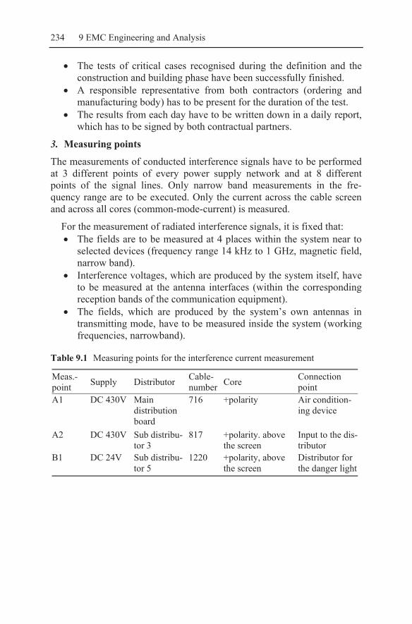
234 9 EMC Engineering and Analysis
• The tests of critical cases recognised during the definition and the construction and building phase have been successfully finished.
• A responsible representative from both contractors (ordering and manufacturing body) has to be present for the duration of the test.
• The results from each day have to be written down in a daily report, which has to be signed by both contractual partners.
3. Measuring points
The measurements of conducted interference signals have to be performed at 3 different points of every power supply network and at 8 different points of the signal lines. Only narrow band measurements in the fre-quency range are to be executed. Only the current across the cable screen and across all cores (common-mode-current) is measured.
For the measurement of radiated interference signals, it is fixed that: • The fields are to be measured at 4 places within the system near to
selected devices (frequency range 14 kHz to 1 GHz, magnetic field, narrow band).
• Interference voltages, which are produced by the system itself, have to be measured at the antenna interfaces (within the corresponding reception bands of the communication equipment).
• The fields, which are produced by the system’s own antennas in transmitting mode, have to be measured inside the system (working frequencies, narrowband).
Table 9.1 Measuring points for the interference current measurement
Meas.-point Supply Distributor Cable-
number Core Connection point
A1 DC 430V Main distribution board
716 +polarity Air condition-ing device
A2 DC 430V Sub distribu-tor 3
817 +polarity. above the screen
Input to the dis-tributor
B1 DC 24V Sub distribu-tor 5
1220 +polarity, above the screen
Distributor for the danger light

9.2 EMC- Test planning 235
Table 9.2 Points for measuring the radiated interferences and the decoupling measurements, points for the measurement of the contact resistances are defined during the tests *
Measuring point Description of the position H1 Near to the static converters H2 In the vicinity of the main distribution board H3 I0 Boundary between EMC-zone 1 and 2 I1 * From 3 devices to ground
4. Definition of the operation modes of the system • Normal operation with 80 % load • Special mode, for the case of emergency power supply
5. Switch on/switch off tests
Two switch on / switch off tests have to be carried out with defined opera-tional modes of the devices.
• Procedure for the 1st test
Commencing with a completely deactivated system, all devices are sequentially switched on up to the radar-, sonar-, and communica-tion equipment according to a switching list. Interferences during the switching actions are to be watched for as the devices are being switched on. In the case of an uncertainty, the corresponding device is to be switched-off again and then switched on once again.
• Procedure for the 2nd test
In the second test, only the devices that are marked as sensitive within the switching list are to be observed. In the second test, all devices are switched on. Subsequently, they are each switched off and on again, one after another. The sensitive equipment is observed for interferences. Sufficient personnel must be available to watch the devices.

236 9 EMC Engineering and Analysis
Table 9.3 Switching list
Device/ device assembly action on/off
sensitive device
description of the in-terference
1 Static converter 1 2 Static converter 2 3 Main switch,
lighting
4 Fire alarm system X 5 Motor assembly 1 6 Speed control unit X 7 GPS-system X 8 Cooling fans with control boards
6. Individual test specifications
A test instruction sheet exists for every single test, containing: • the measuring point, • the frequencies, • the test procedure.
Remarks: The susceptibility test of test sheets 31-34 only have to be carried out, if
the emission tests according to sheets 3-6 and 11-13 deliver values higher than 60 dBμA.
The susceptibility tests of test sheets 35-38 only have to be carried out, if the emission tests according to sheets 18-21 deliver values higher than 100 mV/m.
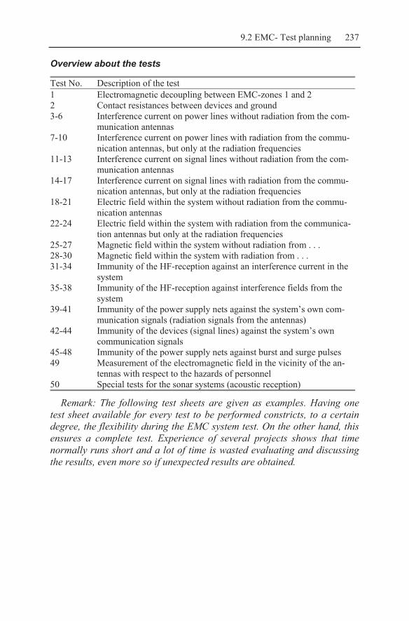
9.2 EMC- Test planning 237
Overview about the tests
Test No. Description of the test 1 Electromagnetic decoupling between EMC-zones 1 and 2 2 Contact resistances between devices and ground 3-6 Interference current on power lines without radiation from the com-
munication antennas 7-10 Interference current on power lines with radiation from the commu-
nication antennas, but only at the radiation frequencies 11-13 Interference current on signal lines without radiation from the com-
munication antennas 14-17 Interference current on signal lines with radiation from the commu-
nication antennas, but only at the radiation frequencies 18-21 Electric field within the system without radiation from the commu-
nication antennas 22-24 Electric field within the system with radiation from the communica-
tion antennas but only at the radiation frequencies 25-27 Magnetic field within the system without radiation from . . . 28-30 Magnetic field within the system with radiation from . . . 31-34 Immunity of the HF-reception against an interference current in the
system 35-38 Immunity of the HF-reception against interference fields from the
system 39-41 Immunity of the power supply nets against the system’s own com-
munication signals (radiation signals from the antennas) 42-44 Immunity of the devices (signal lines) against the system’s own
communication signals 45-48 Immunity of the power supply nets against burst and surge pulses 49 Measurement of the electromagnetic field in the vicinity of the an-
tennas with respect to the hazards of personnel 50 Special tests for the sonar systems (acoustic reception)
Remark: The following test sheets are given as examples. Having one test sheet available for every test to be performed constricts, to a certain degree, the flexibility during the EMC system test. On the other hand, this ensures a complete test. Experience of several projects shows that time normally runs short and a lot of time is wasted evaluating and discussing the results, even more so if unexpected results are obtained.

238 9 EMC Engineering and Analysis
Test sheet No. 1 of the EMC-system test for the project X
1. Test description: Electromagnetic decoupling between EMC-zone 1 and 2
2. Test procedure: Shielding measurements according to NSA-65/6, frequency <30 MHz: magnetic field frequency >30 MHz: electromagnetic field
3. Test frequencies: 1 MHz, 3 MHz, 10 MHz, 30 MHz, 100 MHz 4. Power net: Not applicable 5. Measuring point: I0: Left-hand next to the door between zones 1 and 2 6. Measuring equipment:
Spectrum analyzer, signal generator, power ampli-fier, suitable antennas
7. Measuring bandwidth: 1 kHz 8. Measuring place: Installation place 9. Operational mode: Standard 10. Limit value: 20 dB at least at all specified frequencies 11. Number of plots 12. Remarks:
Test sheet No. 5 of the EMC-system test for the project X
1. Test description: Interference current on power supply lines without ra-diation from the communication antennas
2. Test procedure: CE01/CE03 acc. to MIL -STD- 461, 462 3. Frequency range: 30 Hz....50 MHz 4. Power supply net: DC 24V 5. Measuring point: B1: Sub contribution board 5 6. Measuring devices: Spectrum analyzer, current clamp 7. Measuring band
width: Frequency range Band width 30 Hz .. 20 kHz 100 Hz 20 kHz .. 150 kHz 100 Hz .. 200 Hz 150 kHz .. 30 MHz 1 kHz .. 5kHz 30 MHz .. 400 MHz 100 kHz
8. Measuring place: Installation place 9. Operational mode: Standard 10. Failure criteria: Not applicable 11. Number of plots: 12. Remarks: 1. The + (-) core and the common-mode-current (clamp
above the cable screen) have to be measured and re-corded. 2. The - (+) core has to be checked for similar behav-iour and if necessary an additional recording has to be done.

9.2 EMC- Test planning 239
Test sheet No. 31 of the EMC-system test for the project X
1. Test description:
Immunity of the HF-reception against interference cur-rents within the system
2. Test procedure: As described below 3. Frequency range:
Four frequencies, chosen from the emission test results according to test sheet No. 3
4. Power supply net: DC 430V 5. Measuring point: A1: main switching board 6. Measuring devices:
Frequency generator, power amplifier, spectrum analyzer, current injection clamp, current clamp
7. Procedure: a) Four frequencies with high emissions are chosen from the emission measurements.
b) By use of the current injection clamp a current with low amplitude has to be injected at the same point.
c) The amplitude of the current coupled-in is now raised (but not more than 20 dB above the emission value) until a 3 dB increase in the HF-receiver read-ing is produced.
d) The amplitude of the current has to be recorded. 8. Measuring place: Installation place 9. Operational mode: Standard 10. Failure criteria:
3dB increase for a signal injected, which is smaller than the emission value plus 10 dB.
12. Number of plots: 13. Remarks:

240 9 EMC Engineering and Analysis
Test sheet No. 61 of the EMC-system test for the project X
1. Test description: Electromagnetic field in the vicinity of antennas with respect to personal hazard (RADHAZ)
2. Test procedure: Measuring the electric field during the transmission from the system own antennas using maximum radia-tion power
3. Frequency range: Eight working frequencies of the communication equip-ment
4. Power supply net: Not applicable 5. Measuring points: Points near to HF-antennas accessible for human beings
6. Measuring device: RADHAZ-meter 7. Measuring band-
width: Not applicable
8. Measuring place: Place of operation 9. Operational mode: Standard
10. Measures: Places with field strength values higher than 60 V/m have to be marked
11. Number of plots: Specific delineations have to be produced! 12. Remarks: Possibly the area has to be pre-coloured by chalk
7. Prediction of the interference safety margins
The interference safety margin has to be predicted in each case from the measurements described in test sheets 31 to 48. Once predicted, the fol-lowing four lists must be produced:
• Safety margins between the interference current and the HF-reception
• Safety margins between the interference field and the HF-reception • Safety margins between the radiation from the antennas and the de-
vices, with respect to the currents produced by the radiation • Safety margins between the radiation from the antennas and the de-
vices, with respect to the fields produced inside the system by the radiation
Procedure to predict the interference safety margin
It is known from experience that the prediction of the interference safety margin can be difficult to understanding. Therefore, at this point, the rea-son it is necessary and the prediction procedure is repeated. The particular case of the interference safety margin between interference currents (com-mon-mode, measured across the shield, total effective interference current) on lines and the communication reception is used as an example.
9.2 EMC- Test planning 241
The limit value for the interference current on lines above 100 kHz is derived from the model of disturbing the communication reception (or of other susceptible sensors) by fields produced by this current. The current can be measured quite straightforwardly up to 10 MHz. The measurement of fields in the low frequency range has, for some reason, considerably high uncertainties associated with it. In some cases, the system construc-tion will almost not allow a precise field measurement to be performed. If the limit value for the interference current is defined in an appropriate manner in the low frequency range, the interference potential of a line can be described by a current much better than a field measurement. The cur-rent measured during a system test is only a snap-shot, depending on the operational mode and the impedances during the measuring actions. It cannot be excluded that higher currents may occur. If the communication reception is not disturbed, the safety margin remains unknown. Further-more, it is difficult to associate a noise signal in the radio receiver with a specific noise source. For this reason, it is highly recommended that an in-terference safety margin test is performed. The following procedure may be applied:
A current with low amplitude is injected at a certain place on a line (po-sition where the emission has been measured); ideally a signal modulated to 1 kHz. The radio reception is then observed. A sound at 1 kHz can be easily detected by the human ear. The level should be low enough that the signal is not detected in the radio receiver. Then the level (amplitude of the injected current) is stepped up until the 1 kHz tone can be clearly noticed (3 dB above the undisturbed reading). The necessary current (amplitude) Iinj is recorded. This current is then related to the current Idist measured dur-ing the emission measurement. The interference safety margin can be pre-dicted using the equation
SS inj dista 20log(I / I )= (9.1)
The equation specifies to what degree (expressed in dB) the interference current may increase, until a disturbance in the radio reception can be ex-pected. It is very interesting to note that fixing a 3 dB-increase is con-nected with some difficulties in modern receivers. On the other hand, the human ear is able to notice a 1 kHz-tone with an amplitude 20 dB lower than that detected using a modern, controlled communication receiver. As a result, an amplitude of 3 dB can be calculated from the acoustical detec-tion by a human being.

242 9 EMC Engineering and Analysis
9.3 Execution of analysis
EMC-analyses have been mentioned several times in the previous chap-ters. EMC interference analysis has to be carried out at all development levels, starting with the IC- and PCB-level up to the system level of com-plex systems with antennas. In this sense, the expression ‘EMC-analysis’ is comprehensive in that it comprises simple approximations, for example, using Ampere’s law for predicting low frequency magnetic fields or, per-forming extensive simulation calculations with the help of a computer pro-gram to fix the safety areas around radiating antennas.
A special structure has developed for executing EMC-case studies (analysis of a given situation) that ensures, again, completeness and con-sistency. Furthermore, it makes the EMC-analysis more transparent.
An EMC-analysis is carried out in a straightforward 5-step-procedure.
In the first step, the requirements have to be specified. They may possi-bly read:
“The communication equipment has to operate simultaneously with a frequency offset of > 10 %. In addition, it should operate for the case that one antenna is radiating and another one is receiving.” or
“Visible changes on the monitors of the control equipment are not allowed when the degaussing system is working with its highest currents.”
This first step is normally the simplest but, in many cases, also the most far reaching one. Inadequate requirements may have very far reaching con-sequences.
In the second step, the data of the interference source, of the possible coupling paths, and of the interference victim are collected and written down. This step may be the most time consuming one, but the careful composition of all EMC-relevant data very often points to the solution of the problem. If no, or only incomplete, data is available, assumptions have to be made. In the case of missing data, a convenient solution may be to assume that the device produces emissions equal to the emission limits. Furthermore, it could be assumed that the device has immunity equal to the susceptibility limit of the corresponding standard.
The third step comprises the actual analysis. The interference model has to be produced from the data of the interference source, the interfer-ence victim and the coupling path. This step is, in many cases, the most difficult one. It requires an abstraction of the problem to make an analyti-cal or numerical calculation possible. The degree of abstraction or simpli-

9.3 Execution of analysis 243
fication depends on the quality and completeness of the available data. In addition, it depends on the task and importance of the function being ana-lysed. If the data is inconclusive, or is it not possible to create a model de-scribing the situation sufficiently, laboratory measurements or measure-ments of a comparable construction have to be carried out.
In the forth step measures are proposed to overcome the interference situation, which are derived from the analysis results.
The fifth and final step proposes measurements to verify the results of the analysis and ensure that interferences do not occur.
Example of an EMC-Analysis
On the roof of a shielded radio cabin, a magnetic loop antenna for 24 kHz is installed. Signal lines run inside the cabin, on which an interference cur-rent at 24 kHz may flow.
1. Requirements
The common-mode current (current measured across the cable screen) that is allowed to flow on the cables inside the cabin, in order not to pro-duce a magnetic field higher than 6 nA/m at the position of the antenna, has to be fixed. A comparison of the antenna sensitivity with the atmos-pheric noise has to be executed.
2. Data
Interference source: Cable with common-mode interference current di-rectly below the shielding wall (conducting plane), with a distance of 5 cm to the shielding wall (axis to ground).
Interference victim: Magnetic loop antenna above the shielding wall with a distance of 20 cm to the wall, sensitivity of Hmin = 12 nA/m at 24 kHz, using a bandwidth of 100 Hz and presuming a signal to noise ratio of 6 dB.
Coupling path: Shielding wall made from electro-galvanized steel sheet with a thickness of 5 mm
3. Analysis
It is assumed that the return current flows back with a certain distribu-tion in the shielding wall. The current distribution S(x) can be predicted using a virtual image conductor on the other side of the wall. This return current is indicated by the dotted bell-shaped curve in Fig. 9.1.

244 9 EMC Engineering and Analysis
z
y
x
Idist
s = 5 mm
κ = 0.14r
h = 20 cm
h = 5 cm1
2
H = 6 nA/mmax
Fig. 9.1 Interference model
The surface current (current per unit width) is described by
dist 11 2 2
1
I hS (x)
(x h )= ⋅
π +. (9.2)
The current distribution suffers an amplitude reduction, due to the skin effect, as it travels from one side to the other. The reduction is given by
,)()( 12ds
exSxS−
⋅= (9.3)
where d = skin depth. It is assumed that the bell-shaped current curve re-
mains, but is attenuated according to s
-de . The magnetic field strength pro-
duced by this attenuated bell-shaped current curve is easily predicted using Ampere’s law. In doing so, the following equation has to be evaluated:
sdist 1 2d
2 2 2 2 2 21 20
I h hH (z h ) e dx
(x h ) (x h )
∞−
= = ⋅ ⋅π + π ⋅ +∫ . (9.4)

9.3 Execution of analysis 245
Auxiliary calculation sd
dist 1 22 2 2 2 2 2 2 2 2
2 1 1 20
sd
dist 1 22 2 2
2 1 1 1 2 2 0s sd d
dist 1 2 dist2 22 1 1 2
I e h h 1 1H (z h ) dx(h h ) (x h ) (x h )
I e h h 1 x 1 xarctan arctan(h h ) h h h h
I e h h I e1 12 (h h ) h h 2
− ∞
∞−
− −
⎛ ⎞⋅ ⋅ ⋅= = ⋅ −⎜ ⎟π ⋅ − + +⎝ ⎠
⎡ ⎤⎛ ⎞ ⎛ ⎞⋅ ⋅ ⋅= ⋅ −⎢ ⎥⎜ ⎟ ⎜ ⎟π ⋅ − ⎝ ⎠ ⎝ ⎠⎣ ⎦
⎡ ⎤⋅ ⋅ ⋅ ⋅= ⋅ − =⎢ ⎥⋅ π ⋅ − ⋅⎣ ⎦
∫
1 2(h h )π⋅ +
(9.5)
A very interesting solution is obtained. Specifically, the solution for the magnetic field of a single wire at a distance of r = h1 + h2, which is modi-
fied by the attenuation term s
-de . It has to be remembered that only the cur-
rent within the shielding wall has been considered in this case. For f = 24 kHz and κr = 0.14, a skin depth of d = 1.14 mm is calculable
and with it an attenuation term of ds
e−
= 0.012, corresponding to 38 dB.
Assuming a permitted field of Hmax = 6 nA/m, the allowed current Idist = 0.75 μA (-2.5 dBµA) is predicted.
Comparison of the antenna sensitivity with the outer noise
Converting the antenna sensitivity of Hmin = 6 nA/m into an electric field strength results in Emin = Hmin⋅377 Ω = 2.26 µV/m (7 dBµV/m). This sensi-tivity is specified for a bandwidth of 100 Hz.
According to Fig. 8.3, for 24 kHz and a bandwidth of 100 Hz, it has to be considered with an atmospheric noise that stays between
- 25 dBµV/m (spring time 8 – 12 o'clock) and + 16 dBµV/m (summer time 20 – 24 o'clock)
This demonstrates that the antenna sensitivity has the same order of magnitude as the atmospheric noise.
4. Measures
A displacement of the conductor inside the radio cabin by approximately 2.5 m yields an interference current of approximately 20 dB higher.
246 9 EMC Engineering and Analysis
5. Measurement
Within the EMC-system test on a cable inside the radio cabin, an interfer-ence current is injected. The current, with a frequency of 24 kHz, starts at Idist = -20 dBμA and is slowly increased. The field is measured by an EMC-receiver and a calibrated antenna at a position outside the cabin, which is comparable with the position of the antenna. The injected current is in-creased until an observable ratio of magnetic field strength to interference current can be predicted. The current that produces the specified field of 6 nA/m has to be recalculated from this measurement result. The recalcu-lated current has then to be compared with the analysed one.
Example for applying the measuring procedure
A field outside the cabin of +35 dBµV/m is produced due to a current of +40 dBμA (100 μA) on a chosen cable inside the cabin. The magnetic field strength generally also stated and is given in dBµV/m (H⋅377 Ω).
From a value of +35 dBµV/m, a conversion to a magnetic field strength of -16 dBµA/m can be performed. This leads to a correction factor of k = -56 dB1/m ,
H [dBµA/m] = I [dBμA] + k.
We can deduct that an interference current of -2.5 dBμA flowing on a ca-ble (common-mode) in the cabin, produces a field outside the cabin of
H = -58.5 dBμA/m (1.2 nA/m).
In order to produce an field outside of 6 nA/m (- 44.4 dBμA/m ), a current of I = 12 μA (21.6 dBµA) is necessary.
A discrepancy of approximately 23 dB occurs between analysis and measurement with these chosen values.
Very often ‘worst-case’-assumptions are used within an EMC-analysis, resulting in the reality being generally better than the approximations or calculations.

10 Numerical Techniques for Field Calculation
Programs and program packages for the calculation of electric, magnetic and electromagnetic fields have been developed in parallel to the progress in computer hardware, particularly at universities and research institutes. These programs have been continuously enhanced in performance and adapted to form the current, state of the art computational techniques. Spe-cial schemes have been established out of these developments, which pro-vide professional support for the customer.
Today, a number of powerful program packages are available, which al-low the treatment of nearly all electromagnetic problems in order to an-swer special and also general problems. Through use of the visualisation possibilities provided by modern programs, it is possible to efficiently show the dependency on parameters in arbitrary matter. Electromagnetic processes can be shown with high time resolution; therefore, can provide a perspective into the physical process of coupling. Some coupling and propagation effects will initially be understood through the processing and visualisation of the results.
The situation has to be subdivided when considering the programs as tools of an EMC engineer.
1. If a large company decided to use modern field calculation tools in order to analyse and solve problems involving electromagnetic cou-pling, then, in addition to the programs, well trained personnel is re-quired to operate the programs. These personnel need time to work with the simulation tool and to get used to the program, its capabili-ties and how to operate it. Furthermore, continuous updating of the software is necessary.
2. Very powerful program packages are less suitable for isolating an in-teraction and for helping to solve a compatibility problem without a significant amount of pre-training. Furthermore, the knowledge and creativity of the engineer are needed in any case.
3. The result of a computer simulation is naturally only as good as the model used for the simulation, i.e. the conversion of the real world into a calculable model. It can be assumed that an advanced program
K.-H. Gonschorek, R. Vick, Electromagnetic Compatibility for Device Design and System Integration, DOI 10.1007/978-3-642-03290-5_10, © Springer-Verlag Berlin Heidelberg 2009

248 10 Numerical Techniques for Field Calculation
will deliver correct results with respect to the delivered input. The critical step in using the software is, therefore, the implementation of the physical arrangement in a usable model.
4. The use of a powerful simulation program requires a certain degree of physical understanding. This understanding has to be used to de-cide what details of the real system can be neglected, whilst ensuring that the model can solve a specific problem. Furthermore, it has to be known what geometrical and electrical data effect the result and must be taken into account. A physical understanding is especially needed for assessing and interpreting the results. In general, the result of a modern simulation is either a colourful diagram or a large number of values. These results have to be interpreted with regards • plausibility and physical correctness, • any necessary model refinements.
Some projects (i.e. building of a new naval frigate) require a large amount of numerical calculations with respect to EMC; for example, an-tenna coupling, optimization of antenna locations, antenna impedances and safety in electromagnetic fields. As a result, it may be necessary to subcon-tract parts of the investigation to a professional service provider.
The fundamental theoretical concepts of the main program packages can be roughly divided into
• Boundary matching methods, • Volume methods, • Ray methods.
Furthermore, a large number of supplements, small programs and equa-tions could be of great help for specific problems. A number of possible programs are named and treated within this book.
This chapter tries to give an overview of the possibilities of modern computational techniques, which may be used to work on EMC problems. The theoretical fundamentals of the different methods will be briefly shown and then the preferred applications as well as the limits are dis-cussed. This chapter is not intended as a replacement for specific numeri-cal modelling literature.
A statement discussing the usage of a suitable method will be given in chapter 10.1, based on a flow diagram (Fig. 10.1). Furthermore, the fre-quency limits for the different methods will be given (Fig. 10.2). The dia-grams shown are presented in the style of annex 1 in the German military standard VG 95 374-4 [VG993].
These diagrams were developed by the authors a number of years ago. Annex 1 and 2 of VG 95 374-4 also contain a large number of suggestions

10.1 Selecting the appropriate technique 249
for EMC analysis and for the use of computer technology to model various scenarios. These sample arrangements should be recalculated if the proper software is available and if the reader wishes to gain experience of the nu-merical algorithms.
Possibilities are given in chapter 10.2 to verify results by means of so called plausibility checks. One criterion can be stated verbally as: The con-servation of energy has to be maintained, i.e. the power consumed within the resistors and the power radiated through a closed surface (ideally in the far field) must be equal to the power fed into the arrangement.
Some results of complex simulations are shown in chapter 10.3. This is mostly intended to demonstrate the performance of state of the art com-puter programs (simulation tools), rather than show the application in EMC. Chapter 10.4 gives hints for creating models of real structures that can be calculated numerically. The description of numerical simulation techniques is completed in chapter 10.5, where the coupling between two antennas spaced in close distance is analysed in a practical example.
10.1 Selecting the appropriate technique
A flow-diagram for the selection of the appropriate analytical tool is shown in Fig. 10.1. Following the steps of the diagram, the first question is: Is the analysed structure a wire structure?
A wire structure is not only a power or telecommunication line, but any structure characterised by long and thin electrodes. These structures could be analysed by means of transmission line theory. This has the advantage that it takes only a short amount of time to obtain results. Furthermore, the results are easily to interpret. If transmission line theory, or methods based on it, is not applicable, then the ratio between the geometrical dimension and the lowest wavelength of interest is the next point of concern. The geometrical dimension should be determined using the longest diagonal of the system being investigated.

250 10 Numerical Techniques for Field Calculation
START
END
transmissionline
l < /10λ
l < 10λnetworktheory
applicable
inside aclosed structure
inside aclosed structure
magnetic fieldprevailing
geometric theory of diffraction
finite differences, HF-field(FDTD)
boundaryelementmethods(MOM)
chargesimulation method
strayfieldprograms,mutuelinductances
finiteelements,finitedifferences
netzworkprograms,for instancePSPICE
transmissionline methods
(chap. 10.1) (chap. 10.1) (chap. 10.1) (chap. 10.1) (chap. 10.1) (chap. 10.1, 7.6and A 9)
(chap. 10.1 and A 1)
(chap A 2 and A 3)
yes
yes
yes
yes
no
no
no
Fig. 10.1 Flow-diagram to select the appropriate numerical tool, l = structure
dimension, λ = wavelength
The wavelength at a frequency of f = 100 MHz is 3 m. However, at 1 GHz it is only 30 cm. If the dimension of the structure l is smaller than λ/10 of the highest frequency of interest, one can assume static, stationary or quasi-stationary behaviour. Network theory can be used if the values of the parasitic elements are known or can be estimated. In addition, it can be used when the parasitic elements are negligible. In this case, network cal-culation tools can be applied to obtain usable results.
If network theory cannot be used, a decision has to be made as to whether the structure is placed inside a closed structure or if the field can propagate into open space. In general, a closed structure is assumed if the boundary conditions exist for all 6 surfaces. One can assume a closed structure if the surfaces consist of good conductors. If the arrangement is placed within a closed structure, programs are used based on the finite element or finite difference methods. The electric fields outside of closed structures can be calculated using the charge simulation method. Subse-

10.1 Selecting the appropriate technique 251
quently, the magnetic fields can be calculated by applying the Biot-Savart law.
If the dimension of the structure is greater than or equal to λ/10, high frequency behaviour has to be taken into account, i.e. the time delay be-tween cause and effect. In the microwave range (l > 10…100 λ) one must revert to optical based methods. In the frequency range below this thresh-old, and for closed structures, the finite difference methods for high fre-quencies are suitable. For open structures, i.e. structures that radiate into free space or structures without finite boundaries, integral equation based numerical techniques are used. If the behaviour can be traced back to a de-scription of the boundary conditions (such as the field generating current), one can use the method of moments (MOM) as the main integral equation based procedure. The classification according to Fig. 10.1 serves only as an initial point of reference. Research on programs capable of simulating complex structures is performed at numerous institutions, in particular in the university area. A hybrid method is described in the paper [HE/HA/GO99].
This method combines the advantages of transmission line theory, the integral equation based methods and the theory of geometrical diffraction.
Fig. 10.2 aims to depict the preferred application of the different meth-ods with respect to the wavelength.
network programs,charge simulation method,strayfield programs,mutual inductances
Fig. 10.2 Preferred application of different calculation methods
The integral equation based methods, especially the method of moments (MOM), can be considered as the most important numerical calculation

252 10 Numerical Techniques for Field Calculation
tool for an EMC-engineer. It can be used to find solutions for nearly any kind of electromagnetic problem and guarantees convergence for suffi-ciently dense discretisation.
The different methods are described extensively in literature. A closed description including an objective overview of the different methods is not known. A short introduction into the different possibilities is given in [GO/SI92].
Methods based on transmission line theory
If one is dealing with extended thin structures or parts, such as a single wire above ground or a pair of wires in space, the solutions of current and voltage along the line (See Eqs. (10.1) and (10.2)) can be derived. Neglect-ing the radiated energy the solutions are derived from equivalent circuit of a short section of the line according to Fig. 10.3.
Fig. 10.3 Equivalent circuit of a transmission line section with the length Δz
R’, G’, L’ and C’ are the primary transmission line parameters, which can be calculated from the static or stationary assumptions. Δz denotes the length of the transmission line section.
The solution for the current and the voltage along the line is:
( ) ( ) ( )cosh sinha aU z U z I zγ γ= ⋅ − Γ , (10.1)
( ) ( ) ( )cosh sinhaa
UI z I z zγ γ= ⋅ −
Γ, (10.2)
( ) ( )' ' ' 'R j L G j C jγ ω ω α β= + ⋅ + = + , (10.3)
i R’∆z L’∆z
u (z,t)
(z,t)
G’∆z C’∆z u (z+ ∆z,t)
(z+∆ z,t)i

10.1 Selecting the appropriate technique 253
' '' '
R j LG j C
ωω
+Γ =
+ . (10.4)
The secondary transmission line parameters are γ and Γ, which can be calculated from the primary transmission line parameters. The electromag-netic behaviour of the line can be completely determined if the connected termination impedance and the generator parameters are known. Extending the equivalent circuit of Fig. 10.3 using longitudinal voltage sources (com-pare with Fig. 7.43) calculated from the incident field
( ) zEtzu z Δ⋅−=Δ , , (10.5)
yields a transmission line with distributed sources. A closed solution can be calculated in frequency domain for this arrangement (compare with sec-tion 7.6).
The analysis can be performed in a number of ways:
1. Dividing the line structure into small sections and assigning each section the lumped circuit parameters calculated from the per-unit-length parameters and the length of the sections. This circuit can then be solved using network analysis programs.
2. Using the transmission property of the line (lossless line without dis-persion) allowing signals to be transmitted without distortion be-tween both ends of the line. The time difference results from the propagation delay and can be calculated using the parameters of the line (Bergeron method). The solution of the transmitted signal is the superposition of all forward and reverse traveling parts.
A summary of possible applications of the transmission line theory is given in [SCH94].
Circuit analysis programs
Circuit analysis programs calculate the currents and voltages in a given circuits for given sources and parameters of the discrete parts. Simple net-work calculation tools can be easily programmed using Kirchhoff’s current and voltage laws. State of the art programs should be used according to the

254 10 Numerical Techniques for Field Calculation
manual. The program SPICE1 (PSPICE) is particularly useful, the freeware version ideally suited to a simple EMC analysis.
Methods based on finite elements and finite differences
The methods of finite elements and finite differences are based on the divi-sion of the field area of interest into finitely large elements. Maxwell’s equations are applied in an approximated form on these finite elements. The finite elements, with their border lines, are to be understood as a mesh with cells and junction points.
For the finite difference method, the potential differential equations Δφ = 0 for the electric field, ΔΨ = 0 for the magnetic field
are derived from Maxwell’s equations and are applied in a difference ap-proximation. These difference equations are successively applied at all junctions of the mesh.
For the finite element method, an equation for the energy stored in the field is established
∫∫∫ ⋅⋅⎟⎟⎠
⎞⎜⎜⎝
⎛∂∂
+∂∂
+∂∂
= dzdydxzyx
zyxW 2
2
2
2
2
2
21),,( φφφε (10.6)
and minimized for the node potentials by specification of a function φ(x,y,z). See [SCH93] for more details.
Stray field programs and programs for determination of the mutual inductance
Programs for the calculation of stray fields and mutual inductance are de-scribed in annex A2 and A3.
Charge simulation method
The physical charge distribution that results on a metallic structure, i.e. the surface charge distribution, is substituted by a finite number of point, line, ring or surface patch charges. Superposition of the contributions from these equivalent charges yields the electric field at a specific point. The kind of the substitution charge and its location is preset. Then, the ampli-
1 The Simulation Program with Integrated-Circuit Emphasis was developed at the
University of Berkley in the early 1970s under U.S. government funding and is not proprietary.

10.1 Selecting the appropriate technique 255
tudes of theses charges are calculated using the boundary condition Etan = 0, resp. φ = φi = constant on the surface of the electrodes. The real charge distribution is replaced by n substitution charges. For n substitution charges, n locations are chosen on the surface where the potential is known (contour points). Hence, it is possible to determine the magnitude of the n substitution charges. The complete electric field of the arrangement can be calculated if the values of the substitution charges are known. It can be seen from reading this that the number of charges, and their locations, have a large impact on the result. Further details can be found in the reference [SI/ST/WE74].
Integral equation methods (especially Method of Moments (MOM))
The real charge distribution is represented by substitution charges within this charge simulation method. Using methods derived from the integral equations relevant to EMC (MOM), a current based simulation method can be imagined. The physical surface current (current distribution) is repre-sented by a finite number of substitution currents. The geometry being in-vestigated is divided into different segments or patches. The location and form of the substitution current (local dependency) is assigned to each segment or patch. The amplitude of the current is calculated by solving an equation system with the boundary condition Etan = 0. Further details can be found in the reference [GO/SI92].
Finite differences for the high frequency field
The field space of interest is again divided into segments leading to a two or three dimensional cell structure. One cell defines the computing points for the electric field and another cell is used for the computation of the magnetic field. The two cell structures are interleaved by half the cell size.
The central difference approximation is used for Maxwell’s equations, where
,rot H j Eωε= (10.7)
,rot E j Hωμ= − (10.8)
and one obtains difference equations. These equations are then applied al-ternatively during a time step procedure on all cells. For further details the reader should refer to reference [CH/SI80].

256 10 Numerical Techniques for Field Calculation
Theory of geometrical diffraction
The electromagnetic behavior of geometries in the very high frequency range can be calculated by launching a finite number of discrete rays of an electromagnetic wave. The rays are distinguished between the direct ray, the rays reflected from objects, rays diffracted at edges and corners and rays with creeping paths along convex curved surfaces. A comprehensive description of the theory of geometrical diffraction is given in [MC/PI/MA90].
10.2 Plausibility check
The value of computational electromagnetic for the EMC is undisputable. It has already been stated, that the use of programs for the computation of electromagnetic fields requires a user with a basic knowledge of electro-magnetic field theory and antenna technology. This knowledge is neces-sary to set up models, but is even more important to be able to evaluate and verify the results. Continually using a program allows the user to know in detail its power and also its weakness. The situations where the result needs to be verified by parameter variations are known.
Well-established procedures and physical conditions can be used in or-der to verify the results or to perform plausibility checks. These methods are appropriate in improving confidence and certainty in the results ob-tained.
1. ∑Pi=0 power balance The power balance of a closed system needs to be satisfied. Considering electromagnetic systems in the frequency domain, the following condition of power balance can be derived:
The sum of the power consumed by the resistors and the power radi-ated over a closed sphere in the far-field of the arrangement (power density, Poynting vector) has to be equal to the power fed into the system.
A simple case exists where there is only one feeding point; it follows that:
∑ ∫ ∫ ⋅⋅Γ
+⋅=⋅π π
ϕϑϑ2
0 0
22
22 sin)Re( ddrERIZI iiein , (10.9)

10.2 Plausibility check 257
)Re( einZ = real part of the input impedance at the feeding point,
Ri = ith resistor,
∫ ∫ ⋅⋅Γ
π π
ϕϑϑ2
0 0
22
sin ddrE = power, radiated over the sphere.
A large number of programs based on the method of moments deliver the possibility of calculating and outputting the total power, which is radi-ated over a sphere at far distance. If this option is not available, the power can be estimated by assuming an antenna with a gain of 3 dBi (factor of 2 in the power). The program is then used to calculate the maximum field strength at large distance r. The power radiated over a closed sphere can then be approximated using Eq. (10.10).
2max2
421 rEPrad ⋅⋅
Γ⋅= π (10.10)
This yields a rough estimate, which should have the order of the power calculated according to Eq. (10.9), which is needed to check the power balance of the system.
If this estimation is inaccurate, then the gain can be approximated ac-cording to
41.000D
ϕ ϑ=
Δ ⋅ Δ , (10.11)
where Δϕ is the horizontal and Δϑ is the vertical opening angle of the an-tenna (angle between the 3 dB-points, in degrees) in the arrangement. Equation (10.10) is rewritten as
22max1
4rad
EP r
Dπ= ⋅ ⋅ ⋅
Γ. (10.12)
2. Z12 = Z21, reciprocity of the port parameters A geometrical arrangement consisting of an antenna (source of distur-bance), a complex superstructure and a second antenna (receptor of distur-bance, victim) can be described as a connected two port circuit, as shown in Fig. 10.4.

258 10 Numerical Techniques for Field Calculation
outputimpedance
interference source
interferencesinkII UU11 22Z
Fig. 10.4 Arrangement consisting of source, electromagnetic environment, and
victim
The transfer equation of the two port circuit can expressed in terms of the Z-parameter.
[ ] [ ] [ ]IZU ⋅= (10.13)
The component form is given according to equation (10.14).
.,
2221212
2121111
IZIZUIZIZU⋅+⋅=⋅+⋅=
(10.14)
Assuming linear behaviour (doubling the voltage results in double the current), the two port circuit can be said to be reciprocal, leading to
2112 ZZ = . (10.15)
This condition can be used for a plausibility check. Whereby, according to equation (10.14), it follows:
02
112
1 =
=II
UZ (10.16)
01
221
2 =
=II
UZ (10.17)
Procedure 1. Two ports (port 1 and port 2) are chosen within an arbitrarily complex
arrangement. 2. Terminate port 1 by a high impedance Z1. In general, a resistor of 1 MΩ
is sufficient. 3. Feed port 2 by a voltage, power or current and calculate the current I2
flowing into the port.

10.2 Plausibility check 259
4. Measure and record the voltage appearing across the high impedance
load Z1 , lets say U1, and calculate the ratio ∞=
=1
2
112
ZIUZ .
5. Exchange the functions of port 1 and port 2 regarding the feeding and
termination, then calculate the ratio∞=
=2
1
221
ZIUZ .
6. Comparing the results of steps 4 and 5 should yield 2112 ZZ = .
Remark: This criterion is especially sensitive if different development and weighting functions are used to derive the applied equations. This condition should be primarily fulfilled using the Galerkin method.
3. I
H2 rφ =
πAmpere’s law (global)
Neglecting the displacement current ( D / t∂ ∂ ) in the first Maxwell’s equa-tion, it follows:
.s A
H ds J dA I⋅ = ⋅ =∫ ∫ (10.18)
For a cylindrical conductor with a return conductor in coaxial form or placed in a large distance, it follows:
2I
Hrϕ π
= . (10.19)
The magnetic field Hϕ (tangential component) at a field point is equal to the current flowing in the wire, divided by the distance of the field point from the wire axis, multiplied by 2π (circumference at distance r).
Ampere’s law can be used to verify the results (as an approximation). The magnetic field on the surface of a cylindrical conductor, at a location dominated by the conductor, is calculated, i.e. at a location where the in-fluence of other parts of the geometry can be neglected. The result of the estimation according to equation (10.19) should be of the same order as the result computed using the program.
4. S n x H= Ampere’s law (local) Ampere’s law can also be interpreted locally. Therefore, only a small sec-tion of the surface of the conductor is considered. Due to the skin effect the

260 10 Numerical Techniques for Field Calculation
current flows within a thin layer (see Fig. 10.5). Therefore, a current sur-face density [ ]S A / m can be defined.
Fig. 10.5 Cross section with surface current in a small layer of a conductor
The electric and magnetic field strength reduces rapidly towards the in-ner of the conductor. Correspondingly, the current or the current density also reduces rapidly. At a depth equivalent to 4.6 times the skin depth the values are only 1% of the original surface values.
Choosing the contour s for the integration of the magnetic field H on the surface, with the return integration path at a depth in the conductor, and where H is infinitesimally small it follows, according to equation (10.18):
.xs
H ds H s⋅ = ⋅∫ (10.20)
The current penetrating the surface bounded by the contour s equals
.sSAdJ yA
⋅=⋅∫ (10.21)
Combining both results leads to
Hx = Sy . (10.22)
The field orientation is given by the right hand rule, i.e. the current flows into the surface if the path of integration of the magnetic field H is clockwise with respect to the surface.
In general, this can be expressed in terms of the equation
HxnS = . (10.23)
The relation is depicted by Fig. 10.6.

10.2 Plausibility check 261
Fig. 10.6 Orientation of HandnS ,
Applying this discussion to the plausibility check means that the mag-netic field and the surface current density at specific locations on the sur-face of conductors must be computed. The two values have to be equal. This is not self evident because the two values are commonly calculated using different computing algorithms.
5. Etan = 0 - vanishing tangential field The components of the electric field vector tangential to the surface of an ideal metallic conductor have to vanish (or have to be very, very small). This condition is evident when using the electric field E in order to calcu-late the current density J.
EJ ⋅= κ (10.24)
A tangential electric field of Etan = 1 V/m would result in a current den-sity within copper of
.105711057. 266
tan0 mA
mV
VmAEJ Cu ⋅=⋅⋅== κ (10.25)
The condition on the surface of conductors, Etan = 0, is used as the boundary condition in many programs in order to calculate the unknowns. These unknowns may be the substitution charges within the charge simula-tion method or the substitution currents within the current simulation method.
Obviously, this condition is used and fulfilled for only a finite number of points on the surface. Finite values can occur at other points due to the discretisation used in the program.
The quality of the calculation, hence the model, can be validated by cal-culating the tangential electric field at points that are not being used for solving the equation system, by fulfilling the condition Etan = 0. It is unlikely that the result zero is obtained. Hence, the condition needs to be extended and the normal component of the electric field at the points has to be calculated as well. The ratio between the tangential and normal compo-nent should be smaller than 10-8 to 10-10.
S
n
H

262 10 Numerical Techniques for Field Calculation
108tan 10...10 −−≤normE
E (10.26)
6. [ ] [ ] [ ]1 2 112
s sZ Z E ,
c− −
⋅ = τ = - Satisfaction of mathematical and
physical laws
a) Matrix check
The principle on which the numerical computation of electromagnetic fields is based is in most cases the discretisation of a geometry, in general the spatial discretisation. For each length, patch or volume cell; a function is defined according to the numerical method being used. The weighting or amplitude of this function has then to be determined. The calculation of the weighting may be performed using iterative algorithms or by solving an equation system in matrix from.
The appropriate matrix usually has to be inverted during this calcula-tion. In the case of the method of moments, the impedance matrix is in-verted, which can get large depending on the complexity and discretisation of the problem.
Multiplying the solution matrix (inverse matrix) by the original matrix should yield the unity matrix. Again, values smaller than 10-10 to 10-12 have to be considered as zero.
Therefore, a plausibility check can be performed by comparing the product of the original matrix and the inverse matrix with the unity matrix. Through this method, the quality of the inversion algorithm can be checked and also errors within the model can be found.
The inversion of the matrix leads to random results if the matrix is over-determined or the matrix rows or columns are not mathematically inde-pendent. Such a situation is obtained if two parts of the structure are situ-ated at the same position within a large system. A further situation of uncertainty is encountered, if two lines intersect with a small angle. Hence, their cross sections overlap or wrap, which is not possible from a physical point of view.
The experience of the authors is that a matrix check should be per-formed if one obtains inaccurate results. In general, there is a serious error if a unity matrix is not obtained.
The matrix criterion can be considered as trivial if a stable program code is used and the user has experience in using the code. Here the matrix in-version check can possibly be omitted, especially when considering the computation time. Furthermore, it has to be considered that the matrix in-

10.2 Plausibility check 263
version is normally performed on the same memory space as the original matrix when using current computation techniques. Therefore, only the memory for the matrix and possibly 1 or 2 intermediate vectors is required. The resulting matrix is situated in the original matrix’s space after the in-version is performed. This makes good economic sense with respect to the use of computation resources. Therefore, the original matrix does no longer exists and it would have to be stored on separate space before inver-sion.
If the investigator does not want to waive the matrix check completely, a simplified procedure can be applied. This procedure is sufficient in 98 % of the cases, according to the experience of the authors. In this procedure only the first row of the original matrix is stored and is then multiplied by the first column of the inverted matrix. The result needs to be either a real ‘1’, if computed with real numbers, or a complex 1 (1,0), if computed with complex numbers.
b) Propagation time check
The time delay between cause and effect has to be calculated by dividing the difference between two spatial points by the velocity:
css 12
12−
=τ (10.27)
c) Late time value check
If a step function is used to excite a closed loop circuit containing a capaci-tor, the voltage across the capacitor has to reach its final value for t→∞.
If a closed circuit contains inductors (and resistive loads), the current in the circuit has to reach the DC value for t→∞.
d) Low frequency check
Every program used for simulation in the frequency domain has a lower frequency limit. This frequency limit depends on different influencing fac-tors and on the simulated arrangement itself. State of the art programs based on the method of moments should be able to simulate down to a fre-quency of a few Hz.
In case this is possible, plausibility checks of low frequency solution can be carried out. The DC- or low frequency solutions are produced using network or low frequency procedures, according to annex A1 to A3, and then it is checked whether the solutions of the simulation program con-verge to these DC- or low frequency approximations at low frequencies.

264 10 Numerical Techniques for Field Calculation
Remark: Out of the previous plausibility check it can be concluded that RF simulation tools can generally be used to calculate the capacitance and inductance of complex arrangements. The input impedance of a rod an-tenna at low frequencies can be approximated by
statrad C
jRZω
11 −≈ (10.28)
and the input impedance of a loop by
selfradin LjRZ ω+≈ , (10.29)
where Rrad is the radiation resistance according to table 5.1, Cstat is the static capacitance of the rod antenna and Lself is the self inductance of the loop.
Exercises
Exercise 10.1: The antenna on top of a car radiates a power of 5 W at a frequency of 141 MHz. It is stated, that the electrical field strength of 10 V/m exists at a distance of 10 m. Is this statement possible? Justify your answer.
Exercise 10.2: The beam width angles of a radar antenna are Δϕ = 4° and =Δϑ 6°. What field strength is expected at a distance of 1000 m if a peak
power of 1 MW will be radiated?
Exercise 10.3: The program CONCEPT computes an input impedance of Zin = 40.3 μΩ – j 167 kΩ for a rod antenna over ground at a frequency of f = 10 kHz. The length of the antenna is l = 10 m and the diameter of the rod is d = 2 cm. What is the static capacitance Cstat of the rod with respect to ground?
Exercise 10.4: The program CONCEPT computes an input impedance of Zin = 0 + j 5.1 mΩ for a square loop antenna with a length of l =30 cm and a wire radius of R = 1 cm at a frequency of f = 1 kHz. What is the self in-ductance Lself of the loop?
Exercise 10.5: Two quadratic loops with loop areas of A1 = 0.5 m2 and A2 = 1 m2 are placed parallel to each other at a distance of d = 40 cm on the same axes. The wire radius of both loops is R = 1 mm (See Fig. 10.7).
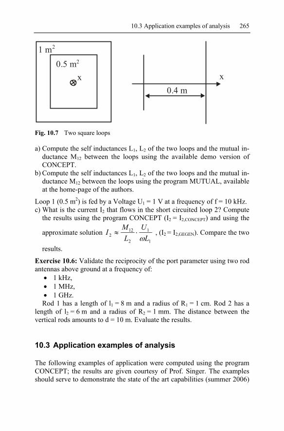
10.3 Application examples of analysis 265
x x
1 m0.5 m2
2
0.4 m
Fig. 10.7 Two square loops
a) Compute the self inductances L1, L2 of the two loops and the mutual in-ductance M12 between the loops using the available demo version of CONCEPT.
b) Compute the self inductances L1, L2 of the two loops and the mutual in-ductance M12 between the loops using the program MUTUAL, available at the home-page of the authors.
Loop 1 (0.5 m2) is fed by a Voltage U1 = 1 V at a frequency of f = 10 kHz. c) What is the current I2 that flows in the short circuited loop 2? Compute
the results using the program CONCEPT (I2 = I2,CONCEPT) and using the
approximate solution 1
1
2
122 L
UL
MI
ω⋅≈ , (I2 = I2,GEGEN). Compare the two
results.
Exercise 10.6: Validate the reciprocity of the port parameter using two rod antennas above ground at a frequency of:
• 1 kHz, • 1 MHz, • 1 GHz.
Rod 1 has a length of l1 = 8 m and a radius of R1 = 1 cm. Rod 2 has a length of l2 = 6 m and a radius of R2 = 1 mm. The distance between the vertical rods amounts to d = 10 m. Evaluate the results.
10.3 Application examples of analysis
The following examples of application were computed using the program CONCEPT; the results are given courtesy of Prof. Singer. The examples should serve to demonstrate the state of the art capabilities (summer 2006)
266 10 Numerical Techniques for Field Calculation
for analysing complex structures with respect to their electromagnetic be-haviour. The example’s importance is only to give the reader a snap-shot of the features of today’s programs and to help the reader make decisions whilst working with such programs.
No other programs are named intentionally. Should the reader be inter-ested, a number of advertisements, including colourful images, for simula-tion tools can be found in the magazines IEEE Transactions on Antennas and Propagation (IEEE TAP) and IEEE Transactions on Electromagnetic Compatibility (EMC).
The examples in this chapter are only briefly described in terms of their geometrical arrangement and electrical parameters.
10.3.1 Investigation of resonances on a passenger car
The resonant behaviour of a passenger car was investigated as part of a project performed for the German Association for Research on Automo-bile-Technique [GO/NE93].
The surface current on well-known car is shown in Fig. 10.8 for 2 dif-ferent frequencies (30 MHz, 40 MHz). The red area (engine hood, brighter area in the 40 MHz figure) indicates high surface currents and the blue (darker area in the 30 MHz figure) indicates a lower surface current den-sity. The car is illuminated by a plane wave impinging from the front of the car; the amplitude is the same in both cases. It can be clearly recog-nised that the car experiences an electromagnetic resonance at a frequency of 40 MHz. Comparing the amplitudes of the current at the two frequen-cies reveals a resonant rise in amplitude of approximately 20 dB. When considering the figures, it should be noted that the simulation was per-formed more than 10 years ago. Coloured pictures are standard when using modern programs.

10.3 Application examples of analysis 267
a)
b)
Fig. 10.8 Surface currents on a car when illuminated by a plane wave from the
front, a) f = 30 MHz, b) f = 40 MHz
10.3.2 Influence of a dielectric material on the radiation of a printed circuit board
In the following example, a 10 cm long trace is placed 0.3 mm above an ideal conducting surface. The electromagnetic radiation of the trace was investigated both with and without the dielectric material (εr = 4.7) of the PCB.

268 10 Numerical Techniques for Field Calculation
Exampe:Radiation from a PCB(PhD-Thesis Leone)
E at f = 800 MHzϑ
Fig. 10.9 Arrangement consisting of a line on a PCB (left), vertical radiation dia-
gram of the arrangement with and without dielectric material (right)
The left image of Fig. 10.9 shows the arrangement being considered. The right image shows the vertical radiation diagram, for both cases, at a frequency of 800 MHz.
A lower radiation is obtained when the dielectric property of the mate-rial is included. This is due to the electrical distance between trace and conducting plane being reduced.
10.3.3 Radiation of a mobile phone
Discussions regarding the impact of electromagnetic radiation on human health have reached a new quality. The existence of the fields, the exact measurement of the electromagnetic fields or statements concerning the penetration of the field into the human body are no longer discussed. To-day, the limiting values of these properties are in discussion. The numeri-cal computation of electromagnetic fields has provided a considerable con-tribution during the characterisation and determination of the fields.
Electromagnetic fields can be adequately measured and predicted using simulation. Therefore, the questions to be answered are associated with as-sessing whether the impact depends on a threshold effect or on the ab-sorbed dose, and whether the amplitude, frequency or modulation has a harmful impact.

10.3 Application examples of analysis 269
A human head with mobile phone and the electromagnetic field gener-ated by the phone at a frequency of 900 MHz is shown in Fig. 10.10. The left image shows the segmentation of the head and the cellular phone; the right image shows the fields penetrating into the head. The head is mod-elled as homogeneous lossy dielectric with a permeability of εr = 49.
The reduction of the wavelength in the dielectric body to D 0 rλ = λ ε is interesting from a physics point of view. The wave travelling around the head travels with the speed of light. The wave through the head travels at approximately only 1/7 of the light speed. At the boundary between dielec-tric material and air, both parts exist. Hence, the boundary condition Etan1 = Etan2 has to be fulfilled at every point at every time.
Fig. 10.10 Radiation of a mobile phone
10.3.4 Electromagnetic field on a frigate
In general, mobile military systems have their own power supply system. Furthermore, the systems have equipment for both internal and external communication, a large amount of equipment for automation and control, high sensitivity sensors and receiving systems, including their required an-tennas. Electromagnetic interference within these systems could lead to fa-tal results.
Therefore, in parallel with the construction and building of a military system, an EMC planning is performed to prevent electromagnetic inter-ferences (See chapter 9!). Electromagnetic field simulations are increas-ingly performed during EMC planning. These include the interference be-tween different radio installations, between the radio installations and

270 10 Numerical Techniques for Field Calculation
electronic equipment; as well as the performance of the radio installation with respect to the feeding point impedance, antenna diagrams and hazard-ous areas.
Fig. 10.11 Frigate with antenna on the control station, radiating at a frequency of
100 MHz, upper picture: surface currents, mid picture: field near the frigate, lower picture: vertical antenna diagram
The numerical calculation results of a frigate with an antenna on the control station, radiating at a frequency of 100 MHz, is shown in

10.4 Guidelines for using numerical methods 271
Fig. 10.11. The upper picture shows the surface currents. The built up field near the frigate is shown in the middle picture and the resulting vertical an-tenna diagram is depicted in the lower picture.
10.4 Guidelines for using numerical methods
The computational packages available today for calculating electromag-netic fields and coupling are so powerful and advanced that during inter-pretation the user can assume that, as an initial analysis, the results based on the inputs given are numerically correct. Incomprehensible or physi-cally nonsensical results can usual be traced back to errors in data input or unsuitable simulation conditions. Possible errors in the input, such as the insufficient segmentation length with respect to the wavelength or an in-correct ratio between the segment radius and length of cylindrical wires, are detected, or even corrected, by most programs. Furthermore, most pro-grams provide a visualisation of the geometrical input data, which enables user detection of major mistakes directly after the input of the data.
Unfortunately, it is not possible to detect all input errors by internal checks within the programs. Therefore, the user has to have a certain amount of physical understanding and engineering creativity. The follow-ing guidelines are designed to show the use of numerical methods for meaningful EMC analysis; they are related primarily to the method of moments (MOM). However, most guidelines are applicable to other meth-ods as well.
The application of numerical calculation is normally performed at two levels:
1. In order to perform rapid checks of physical circumstances, to esti-mate if a coupling can lead to interference, to provide reassurance of physically experienced values or measurement results. It is not of primary interest to include every detail or all influences. The princi-pal goal of the analysis is, however, to provide a yes/no/maybe statement, which can then be used as a guide to the next steps.
2. In order to perform extended numerical calculations to answer ques-tions concerning the system construction, the arrangement of equip-ment or the optimisation of the radio system. These complex simulations are certainly justified when considering the construction and building phase of a complex system. Later changes to the system construction due to a missing, but required, property prove to be more expensive than the cost of numerical cal-culations.
272 10 Numerical Techniques for Field Calculation
An education period in the use of the suitable simulation tool is essential at whatever level the user is working. Once more, the reader is referred to annex 2 of VG 95 374 part 4 [VG933], which presents some results of ex-ample arrangements.
A 5 step algorithm for the analysis of a given or assumed interference problem was proposed in chapter 9.3. This procedure should also be used if the reader is considering the use of a numerical program. According to the procedure, the requirements have to be stated in the first step. Relating to the analysis, this requires a definition of exactly what questions have to be answered by the investigation. The following step is the collection of data for the source of interference, the victim of the interference and the coupling path. The analysis is then performed in the third step using an ap-propriate model. The result of the analysis leads either to the statement ‘not critical as assumed’ or to a specification of measures against the cou-pling. The last step is only mentioned for completeness, which is verifica-tion by measurement. The creation of a model is the most important step within the analysis.
Model creation
The result of numerical calculation is only as good as the model used for the simulation. This can be termed ‘garbage in = garbage out’.
The model has to appropriately describe the physical arrangement and has to be simulated using the software being adequate and capable to ana-lyse the model within finite time. Care has to be taken during the creation of the model. However, the gain of knowledge during the creation of mod-els and the numerical simulations follows an exponential function (1-e-n), n = number of simulations carried out.
Establishing what is physically possible and qualifying the differences between wish and reality will become clear after some simulation and cal-culation. Furthermore, the physical understanding of the coupling proc-esses increases. It soon becomes clear what arrangement is critical and where a less detailed model can be used for the particular situation.
Guidelines for the creation of models
The following remarks relate to calculations in the frequency domain using programs based on the method of moments.
1. Once it is clear what needs to be known and data has been collected, a model has to be created. This means, that the modeller should use an appropriately large sheet of paper and draw a schematic of the interfer-ence situation. The source and victim of interference have a central role

10.4 Guidelines for using numerical methods 273
within the schematic. Sources and victims of interference are recorded including the geometrical and electrical data and the distance between them.
2. The next step is to simplify, if necessary, the sources and victims of in-terference in order to work with the chosen program. If, for instance, the short circuit current at a certain point is of interest, a small resistor (1 mΩ) can be inserted into the model at that point and the voltage is then calculated across this resistor. If the modeller is interested in the open circuit voltage, a very large resistor (1 MΩ) can be inserted at the appropriate position.
3. The next question is associated with the details of the environment (me-tallic) which may have to be included. In order to apply justifiable deci-sions all details have to be related to the wavelength of interest. A me-tallic mast of a naval ship with a length of 16 m has an electric length of slightly more than λ/2 at f = 10 MHz. It is conceivable that it will strongly influence the field of a rod antenna (10 to 12 m long). A rod antenna for use in the VHF frequency range has a length of 0.8 m. At f = 10 MHz the electric length of the antenna is an only little less than 0.03λ. This antenna, therefore, will probably not affect the properties or field of the rod antenna.
Some simple rules can be established from this: a) Parts of the structure < λ/10 only have to be considered if they are
placed near to (distance < λ/4) a victim or source of interference, b) Parts of the structure ≥ λ/4 (with ground reference) or ≥ λ/2 (without
ground reference) have to be considered, even if they are positioned a number of wavelengths away from the victim or source of interfer-ence,
c) Parts of the structure > λ/10 and < λ/2 (λ/4) have to be considered if they are positioned closer than 2λ from the victim or source of inter-ference,
d) Thin parts of the structure lead to sharp resonances with an associated impact at the resonant frequency,
e) Large apertures (large area, large circumference with respect to length) lead to broad resonances and a broadband impact on the EMC.
4. If the investigation has to be performed over a large frequency range, such as 2 MHz to 30 MHz for rod antennas on a large naval ship, the creativity of the engineer relates to: • Increasing the complexity of the model with increasing frequency,
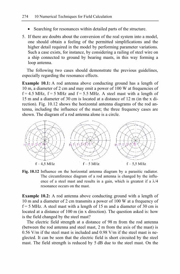
274 10 Numerical Techniques for Field Calculation
• Searching for resonances within detailed parts of the structure.
5. If there are doubts about the conversion of the real system into a model, one should obtain a feeling of the permitted simplifications and the higher detail required in the model by performing parameter variations. Such a case exists, for instance, by considering a railing of steel wire on a ship connected to ground by bearing masts, in this way forming a loop antenna.
The following two cases should demonstrate the previous guidelines, especially regarding the resonance effects.
Example 10.1: A rod antenna above conducting ground has a length of 10 m, a diameter of 2 cm and may emit a power of 100 W at frequencies of f = 4.5 MHz, f = 5 MHz and f = 5.5 MHz. A steel mast with a length of 15 m and a diameter of 30 cm is located at a distance of 12 m (in the x di-rection). Fig. 10.12 shows the horizontal antenna diagrams of the rod an-tenna, including the influence of the mast; the three frequency cases are shown. The diagram of a rod antenna alone is a circle.
Fig. 10.12 Influence on the horizontal antenna diagram by a parasitic radiator.
The circumference diagram of a rod antenna is changed by the influ-ence of a steel mast and results in a gain, which is greatest if a λ/4 resonance occurs on the mast.
Example 10.2: A rod antenna above conducting ground with a length of 10 m and a diameter of 2 cm transmits a power of 100 W at a frequency of f = 5 MHz. A steel mast with a length of 15 m and a diameter of 30 cm is located at a distance of 100 m (in x direction). The question asked is: how is the field changed by the steel mast?
The electric field strength at a distance of 98 m from the rod antenna (between the rod antenna and steel mast, 2 m from the axis of the mast) is 0.56 V/m if the steel mast is included and 0.98 V/m if the steel mast is ne-glected. It can be seen that the electric field is short circuited by the steel mast. The field strength is reduced by 5 dB due to the steel mast. On the
10.5 Application: Antenna coupling 275
other hand, a current flows on the mast. If the magnetic field values are compared, a value of 2.6 mA/m is obtained if the mast is not considered and 18.4 mA/m if the mast is taken into consideration. Therefore, the mag-netic field is magnified by 17 dB.
Exercises
Exercise 10.7: A rod antenna above conducting ground (length l = 8 m, diameter D = 2 cm) emits a power of 100 W at a frequency of f = 30 MHz. A steel mast with a length of 16 m and a diameter of 30 cm is located at a distance of 18 m and welded to the conducting ground. Two sensors are supposed to be located on the mast. Sensor 1 is susceptible to electric fields and sensor 2 is susceptible to magnetic fields. The sensors should be installed as high as possible.
a) At what height hc should the sensor susceptible to electric fields be placed?
b) At what height hm should the sensor susceptible to magnetic fields be placed?
c) Recalculate parts a) and b) for a frequency of 20 MHz. d) Draw the current distribution at a frequency of 30 MHz as function of
the height of the steel mast (obtain from the result of a computer simulation)
e) Calculate the electric field strength E and the magnetic field strength H on the surface of the mast at heights of 15.9 m and 13.5 m.
Exercise 10.8: A shielded cable is installed near a transmitting antenna. The shield is bonded at both ends to the deck of a boat. The cable has a length of l = 8 m between the grounding points.
a) At what frequency is the current on the cable screen at its maximum? At what position does the maximum occur?
b) The cable screen is not bonded at one end due to an installation error. What is the resulting lowest resonant frequency?
10.5 Application: Antenna coupling
10.5.1 General remarks to the N-port theory
In chapter 10.2 (2. Z12 = Z21, reciprocity of the port parameter) it was men-tioned that field coupling problems can be solved using network theory (requirements: linear, time invariant system). The field coupling of the in-volved parts is solved using a method of moments program. If the electri-

276 10 Numerical Techniques for Field Calculation
cal elements (output resp. load impedance) are changed at a later date, it is possible to investigate the effect of these changes on the whole system with a drastically reduced amount of effort. The use of the aforementioned N-port theory for field coupled problems is described in [GON80]. Schla-genhaufer et al. have shown in the paper [SCH/HE/FY03] that the effect of changes in the electric circuitry on the radiation diagram (antenna dia-gram) can be analysed, with much less effort, through the subsequent use of this theory. The idea behind this is that every necessary field point is declared to be a port (imaginary, without self-reaction). Through this as-sumption, only the port coupling between the feeding point, changed cir-cuit and the field point has to be considered. Only a 2x2-matrix and 360 equations (current in the changed ports – field points) have to be solved for an investigation into the effect of a change in the circuit on the horizontal diagram with 360 points.
The application of the network theory to field coupling problems is an interesting starting point for the extended use of field calculation pro-grams, not only for EMC problems. This N-port theory also permits inves-tigations into complete transmission chains including the coupling in, ma-nipulation and re-transmitting.
10.5.2 Two port parameter
A restriction to a two port system is performed at this stage. One port is the feeding port, the other port is the receiving port (including the circuit). The reduction to two-ports makes it easier to understand the relations. Further-more, it has the advantage that principles can be used without many pre-conditions and more than one EMC question can be answered with consid-erably reduced effort. The use of the 2 port analysis is performed here not by matrix manipulations, but by the traditional port parameter definitions. Fig. 10.13 shows the principle 2 port representation.
Fig. 10.13 Two-port representation
This two-port system can be described by the two port parameter:
Input impedance at port 1 with open port 2
I I
U U
1
1
2
2Z

10.5 Application: Antenna coupling 277
01
111
2 =
=II
UZ . (10.30)
Input impedance at port 2 with open port 1
02
222
1=
=II
UZ . (10.31)
Transfer impedance from port 1 to port 2
1201
221
2
ZI
UZI
===
. (10.32)
The box labelled with Z, representing the Z-parameters (Fig. 10.13) can be an arbitrary complex network consisting of directly coupled and field coupled elements, for example, the interaction between a radio amateur (antenna input = port 1) and the electronics of an air bag (base of the input transistor = port 2). If the Z-parameters according to equations (10.30) to (10.32) are known, then it is possible to determine the reaction at one port due to a change at the other port through simple equations.
The Z-parameters are obtained by the complete calculation of the sys-tem. The system needs to be calculated twice if matrix manipulation is not used. The extraction of the elements Z12 and Z21 has already been stated in chapter 10.3. The values Z11 and Z22 are obtained in a similar way.
After the elements Z11, Z22 and Z12 = Z21 are determined, the problem can be solved on the network level and all equations can be used in order to calculate the parameters needed. As an example, one can calculate the input impedance Zin1 at port 1 with a loaded port 2 according to
11 22 12 21211122
1 1122 22 2
2
1L
inL
L
Z Z Z ZZZZZ ZZ Z Z
Z
⋅ − ⋅+
= = −++
, (10.33)
where Z2L = load impedance at port 2.
In order to obtain Z11 and Z12, port 2 is terminated by a high load resistor (1 MΩ should be sufficient). The supply voltage U1 divided by the current I1 going into the circuit yields Z11. Then, dividing the resulting voltage U2 at port 2 by the current I1 yields Z21.

278 10 Numerical Techniques for Field Calculation
If port 1 is terminated by a high-impedance and port 2 is fed, then Z22 is calculated by dividing the supply voltage by the feeding current. Reference [BOE02] may be used for more information about the use of network pa-rameters. Furthermore, transformations into the Y-, C- or H- parameters are presented as well as their meaning.
10.5.3 Calculation of antenna coupling
Through use of the Z-parameters, it is possible to perform parameter stud-ies in a simple and economic way. The following examples are given:
1. If the input impedance of a victim is not known or questionable, then the maximum coupling can be found by a variation of this input imped-ance as load impedance Z2L.
2. Communication antennas should be matched in order to obtain optimal radiation properties. Furthermore, the matching should exist with a specified tolerance in case of circuit changes of others antennas or changing ambient conditions. This quite often needs to be investigated.
3. If one intends to achieve two aims using a specific measure, an exten-sive number of iterations will need to be performed. These iterations can be efficiently performed using the two-port analysis. Antenna op-timisation is named here as an example, where the use of one antenna in different bands is wanted by use of wave traps, filters or extension coils. This task can also be specified with respect to EMC in the follow-ing manner: a disturbing signal has to be suppressed in a way by which the input impedance is only changed by a minimal amount. An addi-tional degree of freedom can be introduced through the arrangement of discrete filter circuits at the antenna elements itself (i.e. within the run of the antenna).
4. The operation of closely spaced antennas at the same frequency or with a small frequency displacement is especially critical if one antenna transmits a specifiable power. Of interest are the mutual passive inter-action (change of the input impedance of one antenna due to a change of the circuit at the other antenna) and the mutual active interference (coupling of energy from one antenna to the other). Further details can be found in [MO/KO80] and [GON84].
In order to demonstrate the use of the two-port parameters, the example of a naval ship design is shown below. Two rod antennas are situated on both sides of a ship mast, which has a height of 18 m and a diameter of 40 cm. Both rod antennas are symmetrically located with respect to the

10.5 Application: Antenna coupling 279
mast at a common distance of 16 m. The rod antennas have a diameter of 2 cm. The arrangement is shown schematically in Fig. 10.14.
Fig. 10.14 Arrangement of two rod antennas on both sides of a mast on a ship
Through the use of matching circuits at both antennas, it is assured that the matching for power transfer is obtained for transmitting operation. The transmitted power is 200 W for both antennas.
During the test phase it occurred that both antennas were operated at the same frequency, i.e. f = 2 MHz. The following investigations had to be performed for this arrangement:
1. What is the input impedance of antennas in the case of power matching of both antennas? This value has to be compared with the value in case of grounding the second antenna.
2. What is the theoretical power coupled from one antenna to the other in the matched case? Losses have to be neglected.
3. What is the change of the horizontal antenna pattern due to the second matched antenna?
The Z-parameters Z11, Z22, Z12, Z21 have to be calculated initially accord-ing to the procedure outlined previously. Due to the system symmetry Z11 is equal to Z22 and the problem is somewhat reduced. CONCEPT was used for the following investigations. The following values are obtained if the antenna on the right hand side is terminated with a load R2 = 1 MΩ and the antenna on the left hand side is driven by a power of 200 W:
U1 = 6 819.6 V, I1 = 0.0293 + j 10.369 A,
xy
z
12 m
18 m
12 m
40 cm
2 cm
2 cm
16 m

280 10 Numerical Techniques for Field Calculation
U2 = - 33.89 – j 16.96 V.
The following Z-parameters are calculated from these values: Z11 = Z22 = 1.86 - j 658 Ω, Z21 = - 1.64 + j 3.26 Ω.
The input impedances for the matching of power transfer need to be cal-culated in the next step. Power matching is obtained if the output imped-ance of the amplifier (in this case a matching circuit in front of the an-tenna) is equal to the complex conjugate of the input impedance of the antenna. First order matching is achieved if the antenna on the right hand side (antenna 2) is terminated by the complex conjugate impedance
*222 ZZ L = .
The input impedance of the antenna on the left hand side (antenna 1) is changed due to the aforementioned interaction and therefore the matching has to be readjusted. Consequently, this again has an interaction with an-tenna 2. Therefore, complete power matching is only obtained after an it-erative sequence.
The procedure is understandable, if one considers the analogy of two ra-dio operators attempting to match their antennas using a matching unit. The radio operators are going to match the units through sequential turns. Therefore, the first operator matches his antenna until power matching is obtained. The second radio operator then matches his antenna. After that, the first one notices the matching is no longer achieved and readjusts his unit until power matching is again reached. Subsequently, the second radio operator notices a mismatch, and so on. The iteration procedure continues until a final value is reached, which provides power matching of both an-tennas.
The source code, written in BASIC, for a very small program called MATCH is given in chapter 10.5.4. The program calculates the values Z11, Z22, Z21, Z12 and Zopt1, Zopt2 from the specified complex values of U1, I1 and U2 for the open circuit operation of antenna 2, and U2, I2 and U1 for the open circuit operation of antenna 1.
Zopt1, Zopt2 are the optimal load impedances needed for power matching of the antenna. The maximum power is dissipated at the receiver of the an-tenna by termination of antenna 2 by Zopt2. In this case the input impedance of the antenna 1 is given by Zopt1
*.
Using the values of the example yields: Zopt1 = Zopt2 = 1.76 + j 655 Ω.

10.5 Application: Antenna coupling 281
Grounding antenna 2 at the feeding point yields Zein1 = 1.84 – j 658 Ω.
as the input impedance of antenna 1. Terminating antenna 2 with Zopt2 and transmitting 200 W at antenna 1 yields a coupled power of
2 22 opt22 I Re(Z )=8.4 ×1.76 W=124 WP ⋅= .
Fig. 10.15 shows the antenna diagrams for the two cases: a) Bonding of antenna 2 at the feeding point, b) Terminating antenna 2 with the optimal impedance Zopt2.
Fig. 10.15 Antenna diagrams of a rod antenna with a second rod antenna located
nearby, a) second antenna bonded at the feeding point, b) second an-tenna optimally terminated
It is interesting to note that antenna 2 receives more than 50% of the ra-diated power of antenna 1. This can be seen in the antenna diagram as well, which shows a directivity effect without a major impact on the field strength in the main beam direction.

282 10 Numerical Techniques for Field Calculation
Exercises
Exercise 10.9: Two rod antennas above conducting ground with lengths of l1 = 12 m and l2 = 16 m, and diameters d1 = 4 cm and d2 = 2 cm, have a lat-eral distance between them of D = 10 m.
a) What are the values of Z11, Z22, Z21 and Z12? b) What is the maximum power transferred from antenna 1 to antenna 2?
Recalculate the results for frequencies of f = 1 MHz, f = 3 MHz and f = 18 MHz.
c) Discuss the general findings of the results.
Exercise 10.10: A centre fed dipole with a length of 5 m (diameter of the rod d = 1 cm) is used at a height of 3 m above a conductive ground at a fre-quency of 25 MHz (a little less than the λ/2-resonance). The transmitter has an output impedance of 50 Ω and an output power of 100 W. The an-tenna should be used in a power matched mode by means of a matching unit.
a) What is the value of ZA2, the input impedance of the antenna match-ing unit seen from the antenna?
b) What is the value of ZA1, the input impedance of the antenna match-ing unit seen from the amplifier?
c) What power is now radiated? In a second case, the dipole is fed di-rectly from an amplifier with an output impedance of 50 Ω.
Exercise 10.11: The following Z-parameters, at a frequency of f = 3 MHz, are known for a two antenna arrangement (victim and source of distur-bances):
Z11 = (5.866 – j 338.8) Ω, Z22 = (11.48 – j 234.5) Ω, Z12 = Z21 = (-7.57 + j 6.58) Ω.
The load impedance of the victim is unknown. All values on the right hand side of the impedance plane are possible.
a) Draw the locus diagram showing the input impedance Z11 of the source depending on the imaginary part of the load impedance (2. Antenna) Z2L.
b) Interpret the result.
Exercise 10.12: A rod antenna above conducting ground with a length of l = 5 m and a diameter of d = 1 cm has to be tuned to a resonance (Im(Zin) = 0) at a frequency of 14 MHz using an extension coil at half height.

10.5 Application: Antenna coupling 283
Is this possible? What would the value of the coil have to be?
10.5.4 Source code of the program MATCH
10 rem Program for determining the optimal load impedances 20 rem in antenna coupling 30 rem ================================================== 35 rem *********version 21.04.2004*************** 40 cls 50 Print "": Print "Values for the mode – no load at antenna 2!" 60 input "real part U1? ", ru12 70 input "imaginary part U1? ", iu12 80 input "real part I1? ", ri12 90 input "imaginary part I1? ",ii12 100 input "real part U2? ",ru22 110 input "imaginary part U2? ",iu22 120 print "": Print "Values for the mode – no load at antenna 1!" 130 input "real part U1? ", ru11 140 input "imaginary part U1? ",iu11 150 input "real part U2? ",ru21 160 input "imaginary part U2? ",iu21 170 input "real part I2? ",ri21 180 input "imaginary part I2? ",ii21 300 call komdiv (ru12,iu12,ri12,ii12,rz11,iz11) 310 call komdiv (ru21,iu21,ri21,ii21,rz22,iz22) 320 call komdiv (ru22,iu22,ri12,ii12,rz21,iz21) 330 call komdiv (ru11,iu11,ri21,ii21,rz12,iz12) 400 print "":Print "Z11 = ";rz11;" + j ";iz11;" Ohm" 410 print "Z22 = ";rz22;" + j ";iz22;" Ohm" 420 print "Z21 = ";rz21;" + j ";iz21;" Ohm" 430 print "Z12 = ";rz12;" + j ";iz12;" Ohm" 500 rz2l = rz22: iz2l = -iz22: goto 600 600 call zein (rz11,iz11,rz21,iz21,rz22,iz22,rz2l,iz2l,rzopt1,izopt1) 610 Print "Zopt1 = ";rzopt1;" + j ";-izopt1;" Ohm" 650 rz1l = rzopt1: iz1l = -izopt1 700 call zein (rz22,iz22,rz12,iz12,rz11,iz11,rz1l,iz1l,rzopt2,izopt2) 710 print "Zopt2 = ";rzopt2;" + j ";-izopt2;" Ohm" 800 input "Do you want another iteration (y/n)? ",A$ 810 if A$ = "n" goto 1000 900 rz2l=rzopt2:iz2l=-izopt2: goto 600 1000 print "":print "An optimal coupling from antenna 1 to antenna 2" 1010 Print "is given, when antenna 2 is loaded " 1020 print "by Z2l = ";rzopt2;" + j";-izopt2;" Ohm!" 1030 print "==================================="

284 10 Numerical Techniques for Field Calculation
10020 end sub komdiv (ra,ia,rb,ib,re,ie) qu = rb*rb+ib*ib re = (ra*rb+ia*ib)/qu ie = (ia*rb-ra*ib)/qu end sub sub kommul (ra,ia,rb,ib,re,ie) re = ra*rb-ia*ib ie = ia*rb+ib*ra end sub sub zin (ra,ia,rb,ib,rc,ic,rd,id,re,ie) call kommul (rb,ib,rb,ib,rz,iz) rnn = rc+rd: inn = ic+id call komdiv (rz,iz,rnn,inn,rzt,izt) re = ra-rzt: ie = ia-izt end sub

11 Model for Immunity Testing
Manufacturers and users of electronic equipment may have experienced equipment, which has passed an EMC immunity test, failing in a real elec-tromagnetic environment. Even repetitive may produce different test re-sults. Furthermore, sudden failures of electronic equipment in a real elec-tromagnetic environment, which can be interpreted neither by the type nor the amplitude of a disturbance, might cast doubt over the interpretation of standardised immunity tests.
Different models for the description of the immunity of electronic equipment are shown and compared in this chapter. The main focus is based around the questions: why is the reproducibility of immunity tests against electromagnetic disturbances not possible in every case and how should manufacturers and users interpret the test results of such equip-ment?
The interaction between an electromagnetic disturbance and electronic equipment or systems is a complex physical process, which is influenced by a large number of electrical and non-electrical phenomena. The result of all this aspects will lead to a specific response of the observed object. By definition, the electromagnetic compatibility of a piece of equipment is given when it shows on one hand, as a source of disturbance, a tolerable level of emissions of electromagnetic energy and on the other hand, as an victim, a sufficient immunity to electromagnetic disturbances. The sensi-tivity to electromagnetic interactions is of high priority when considering the safety of electronic equipment.
The immunity against an electromagnetic disturbance is defined as the ability of electronic equipment to work in the presence of electromagnetic disturbances without faults or damage.
The interpretation of immunity tests is discussed within this chapter and general methods to determine the immunity of equipment are shown. These methods are analysed according to the limits of their application. A stochastic interpretation of the immunity is introduced, which is especially helpful for the interpretation of immunity test results and for the develop-ment of special test procedures for safety related equipment.
K.-H. Gonschorek, R. Vick, Electromagnetic Compatibility for Device Design and System Integration, DOI 10.1007/978-3-642-03290-5_11, © Springer-Verlag Berlin Heidelberg 2009

286 11 Model for Immunity Testing
11.1 Standardised immunity test methods
The immunity depends on a number of environmental conditions, such as temperature, humidity and air pressure. An interval of acceptance is de-fined for the main influences in standardised immunity tests in order to en-sure the reproducibility of the tests.
The electromagnetic compatibility of equipment is confirmed by testing the EUT using a number of standardised test methods. Therefore, a number of fundamental stimuli have been defined in the past. These stimuli should be appropriate for describing the electromagnetic conditions in commonly encountered environments. This is a compromise between affordability of testing and the real physical phenomena. A general model describing the specific environment, which is derived from the frequency domain spectra of the disturbances and the complex physical mechanism of the equip-ment’s disturbance, is not possible for all cases. Strictly speaking, an im-munity test leads to the statement that the tested equipment was either im-mune or susceptible to a specific electromagnetic disturbance, with a specific coupling mode with respect to the defined interface and test condi-tions.
A description of the immunity with respect to the environmental condi-tions and the test disturbances is not possible.
The function of the equipment can be analytically described by an op-erator according to [Ha92] by
][eOpa = . (11.1)
The operator Op[...] represents a functional rule according to which the outputs a will be calculated from the inputs e. The operator can be any rule, even a fabricated one and it may also depend on the internal states and the inputs themselves. The technical realisation is performed by the hardware or software of the equipment. The system element might be in-fluenced by electromagnetic and non-electric quantities. This influence re-sults in a dependency of the operator on the external and internal distur-bances, as well as on the tolerances of the parts and the manufacturing.
The difference between the real operator function Opr [...] and the ideal operator function Opi [...] in the case of impacting disturbances can be de-scribed according to Eq. (11.2) by ΔOP .
][][ eOpeOp irOP −=Δ (11.2)
If the equipment continues to operate as intended without degradation, the difference ΔOP can be said to be below a limiting value ξ. The equip-ment can be defined as functional.

11.1 Standardised immunity test methods 287
ξ<ΔOP system functional (11.3)
If the functioning of the equipment degrades below a performance level or a loss of function occurs, the equipment performs a malfunction. In this case, the difference ΔOP will be equal to or higher than the limiting value ξ.
ξ≥ΔOP system malfunctioning (11.4)
Finally, the threshold of disturbances with respect to the disturbing quantity is reached if the difference between real and ideal operation is equal to the limiting value ξ .
ξ=ΔOP threshold of disturbance (11.5)
A sharp transition between the functional and malfunctioned states of the equipment is assumed by this model, i.e. the immunity has a threshold property. This is depicted in Fig. 11.1.
Level of Disturbance
Diff
eren
ce fr
om F
unct
ion Δ
OP
Limiting Value ε
Thre
shol
d of
Sus
cept
ibili
ty
Level of Disturbance
Occ
urre
nce
of M
alfu
nctio
ns
0
1
Threshold of Susceptibility
Fig. 11.1 Illustration of the susceptibility threshold
During immunity testing, an EUT will be stressed at a defined port GSk by test disturbances Xj from the test generator under defined test condi-tions PB. The parameters of the test disturbance Xj are normally varied, starting from a low level to a higher disturbance level, until the immunity threshold of the equipment is reached.
The susceptibility of the equipment to these external disturbances Xj, under the defined test conditions PB and at the port GSk, can then be de-scribed using the value of the disturbance at which the first malfunctions occurred:
.),,ˆ( PBGSXSF kjj = (11.6)
This truly deterministic approach assumes a threshold property of the immunity, i.e. the susceptibility SF is a constant property of equipment be-

288 11 Model for Immunity Testing
ing tested. This implies that the same susceptibility will be evaluated if the test is repeated under the defined test conditions.
Standardised immunity test methods are based on this deterministic model, which is especially valid for tests against impulsive disturbances.
11.2 Statistical approach to model the immunity
Even if the test conditions are constant within a predefined margin of ac-ceptance, the results of immunity tests against impulsive disturbances, such as ESD or EFT (electrical fast transient), are not reproducible in every case. The result will vary within a certain limit. The outcome of the test exhibits stochastic behavior due to a number of factors, including a change in non-electric factors, the kind of previous electromagnetic stress, the statistical behavior of the properties of the components used, the exis-tence of different susceptible time slots and the complexity of the interac-tion.
Similar phenomena can be observed if the nominal voltage of high volt-age apparatus is being determined.
A test of a programmable logic controller (PLC) against an electrostatic discharge was performed. During the test, with a fixed ESD-generator, the voltage level was increased from low values to higher values until a mal-function of the equipment was observed. The associated malfunction volt-age was then assigned to be the disturbance threshold of the PLC.
The varying disturbance threshold plotted as a function of the test num-ber during a repetitive test of the equipment is shown in Fig. 11.2.
The observed variance of the threshold, even with constant testing con-ditions, shows the lack of reproducibility exhibited.
In order to derive a model for this behavior a classification of the test object was done.
The following two cases can be distinguished, depending on the influ-ence of the timing on the immunity:
1. Time invariant susceptibility
2. Time variant susceptibility

11.2 Statistical approach to model the immunity 289
0
1
2
3
4
5
6
7
1 11 21 31 41 51 61 71 81 91 101
Number of Repetition
Dis
turb
ance
Thr
esho
ld in
kV
Fig. 11.2 Variation of the assessed disturbance threshold of a PLC against ESD
during repetitive testing
A time invariant susceptibility can be assumed if only a certain state or condition of the equipment is considered. This might be the case if a logi-cal gate is driven with well defined logical input signals. In general, how-ever, these input signals will change at the input of a circuit depending on the applied function. This leads to a time variant susceptibility.
These two cases will be more closely analysed in the following sections.
11.2.1 Malfunction probability
It is more useful to model the susceptibility rather than the immunity. The time invariant susceptibility of a EUT can be accurately described by its malfunction probability, i.e. the probability of a malfunction occurring at a given level of applied disturbance.
A requirement, which allows this approach to be used, is that the states of the equipment are decoupled from each other and that an explicit asso-ciation between the disturbance and the malfunction can be carried out.
A malfunction should not further influence the behavior of the equip-ment nor should it lead to aftereffects. In this case, the occurrences of mal-functions only depend on the disturbances at the beginning of the observa-tion period. The susceptibility of the EUT can be modeled as a static stochastic system over a fixed observation period. As the application of

290 11 Model for Immunity Testing
disturbances is on a fixed interface or port, the system can be described simply by only one input and one output.
This causality between the disturbance and the effect has to be ensured for all circumstances. Particularly when considering indirect effects in the case of transient disturbances, which need to be correctly distinguished, as the change of registers may not occur during the observation period.
In order to describe the malfunction probability, K denotes the occur-rence of malfunctions as result of a specific disturbance. Furthermore, K is the complement of K, which would describe the operation of the equip-ment without malfunction.
The reaction of the equipment to an external disturbance is a stochastic variable Y, which is defined within the space of the elementary events
Ω= K,K . A malfunction as result of a disturbance can, but does not have
to, happen. The amplitude is parameter of preference when describing impulsive
disturbances. The behavior of the equipment can be described by a mal-function probability
pm(Û) (11.7)
if a certain value for the disturbance U = Û exists at the input port of the equipment.
It is a measure of the probability of malfunction occurring at a given level of applied disturbances and defined test conditions. The malfunction probability can be used as a complementary quantity for the immunity of the equipment and is given by
pi(Û)=1- pm(Û*). (11.8)
The malfunction probability pm(Û), as a measure of the susceptibility of equipment at a certain time, gives the probability of malfunctions due to a given level of applied disturbances Û.
The malfunction probability pm(Û) can not be directly measured. It can only be estimated after applying a number of test pulses during an immu-nity test.
The aim of an immunity test is to determine the malfunction probability for a given level of an applied disturbance. The fault frequency h can be used as a first step in estimating the malfunction probability. The fault fre-quency is defined as the ratio of observed malfunctions k to the number test pulses n applied,
11.2 Statistical approach to model the immunity 291
nkh = . (11.9)
The estimation of the mean malfunction probability through this method has a naturally large uncertainty associated with it, which can be quantified by means of mathematical statistics. In the case of a constant malfunction probability of the EUT during the test, the methods of statistical interval estimation can be used.
Consider the case that the application of n test pulses of amplitude Û re-sults in k malfunctions. Then, one can state with a statistical confidence ß that the malfunction probability, pm(Û), of the EUT to the test disturbance is in the confidence interval [pu; po]. This is illustrated in Fig. 11.3. p
kn
Lower confidence interval pu = pu(n,k,ß)
Upper confidence interval po = po(n,k,ß)
Observed fault
frequency
ß - confidence interval for the
malfunction probability p
dmax
Fig. 11.3 Interval estimation of the malfunction probability
Out of the observation of an EMC immunity test it is possible, with a certain inherent risk, to give a region in which the immunity will be fluctu-ate in following tests. This fluctuation margin is quite large if only a small number of test pulses were used. In order to decrease the confidence inter-val, it is necessary to increase the number of applied test pulses, which is equal to an increasing testing time. Depending on the application of the equipment it is advisable to find a compromise between the test period and the confidence.
In case of single pulse test, as with the ESD test, the estimation of the confidence intervals can be performed using the assumption of binomial distributed occurrences. It is a requirement that the effects of test pulses do not superimpose and the energy of the test pulse is attenuated completely before a new test pulse impinges on the equipment. Therefore, a sufficient time interval between two test pulses is required.
In [AN91] and [Ni/Os90] it was shown, that under the assumption of a time invariant susceptibility of the EUT, a Bernoulli scheme can be used to

292 11 Model for Immunity Testing
estimate the confidence interval. The occurrence of a malfunction due to an applied test pulse is referred as event K. The unknown malfunction probability pm(Û) can be estimated by repeating the test, with the binary outcome K or K , n-times. The number of occurrences K during the test is labeled by k. The obtained fault frequency h converges according to the statement of Bernoulli towards the unknown malfunction probability pm(Û). The precision is dependant on the number n of applied test pulses.
Using the Binomial distribution, it is possible to estimate a confidence interval [pu;po] for the malfunction probability with a given statistical con-fidence β. For two sided interval estimation, Eqs. (11.10) and (11.11) are applicable.
2/)1();(2);1(2
2/)1();(2);1(2
)1()1(
β
β
+−+
+−+
⋅++−⋅+
=knk
knko Fkkn
Fkp (11.10)
2/)1();1(2;2
2/)1();1(2;2
1 β
β
−+−
−+−
⋅++−⋅
=knk
knku Fkkn
Fkp (11.11)
The following notation is used: pu Lower confidence limit of the malfunction probability p po Lower confidence limit of the malfunction probability p k Number of observed malfunctions n Number of applied test pulses β Statistical confidence Fl,m,p Quintile (fraction of points below a given value) of the
F-distribution with the degree of freedom l, m and the order p
The necessary quintile of the F-distribution are given in tables of mathematical statistics. Usefully, modern spreadsheet programs can be used to implement the quintile as formula (i.e. FINV). Therefore, a calcu-lation of the confidence interval can be easily performed.
11.3 Fault frequency function
If the malfunction probability pm(Û) was determined at different voltage levels, it is possible to estimate the function pm(u).
This function is the probability distribution function of the EUT’s im-munity. It gives the value of the malfunction probability pm(Û) at a given level Û of the disturbance being investigated.

11.3 Fault frequency function 293
Amplitude of the Disturbance U*
h, p
in %
0
20
40
60
80
100
pupo
Immunity described by the fault frequency h Deterministic approach
assuming a step function
Fig. 11.4 Behaviour of the malfunction probability distribution and the determi-
nistic assumption
The fault frequency function in Fig. 11.4 depicts the dependency of the fault frequency on the amplitude of the disturbance. The uncertainty is quantified by the calculated confidence interval for each level of distur-bance.
The determined fault frequency function can be fitted to mathematical distribution functions. Therefore, special algorithms are implemented in statistical software packages, which allow the estimation of the parameters of the theoretical distribution function from random test samples.
The empirical fault frequency function of a programmable logic control-ler (PLC) during a test of the immunity against electrostatic discharge is depicted in Fig. 11.5. Due to missing monotonic behaviour, the empirical fault frequency function can not be fitted to mathematical probability dis-tributions.
It has been shown that a difference exists between the provable results of immunity tests and the deterministic interpretation of standardised im-munity tests. A way to solve this discrepancy is the introduction of statisti-cal improvements in describing the immunity.
The statistical immunity, in the case of electromagnetic disturbances, is the property of the equipment or system, which exhibits with a large statis-
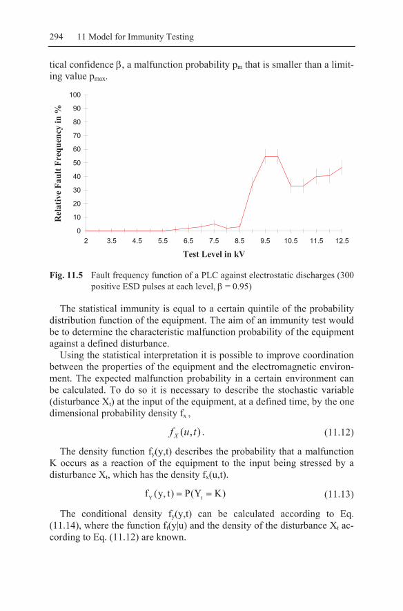
294 11 Model for Immunity Testing
tical confidence β, a malfunction probability pm that is smaller than a limit-ing value pmax.
0
10
20
30
40
50
60
70
80
90
100
2 3.5 4.5 5.5 6.5 7.5 8.5 9.5 10.5 11.5 12.5
Test Level in kV
Rel
ativ
e Fa
ult F
requ
ency
in %
Fig. 11.5 Fault frequency function of a PLC against electrostatic discharges (300
positive ESD pulses at each level, β = 0.95)
The statistical immunity is equal to a certain quintile of the probability distribution function of the equipment. The aim of an immunity test would be to determine the characteristic malfunction probability of the equipment against a defined disturbance.
Using the statistical interpretation it is possible to improve coordination between the properties of the equipment and the electromagnetic environ-ment. The expected malfunction probability in a certain environment can be calculated. To do so it is necessary to describe the stochastic variable (disturbance Xt) at the input of the equipment, at a defined time, by the one dimensional probability density fx ,
),( tufX . (11.12)
The density function fy(y,t) describes the probability that a malfunction K occurs as a reaction of the equipment to the input being stressed by a disturbance Xt, which has the density fx(u,t).
Y tf (y, t) P(Y K)= = (11.13)
The conditional density fy(y,t) can be calculated according to Eq. (11.14), where the function ft(y|u) and the density of the disturbance Xt ac-cording to Eq. (11.12) are known.

11.3 Fault frequency function 295
Y t X Stör X0 0
f (y, t) f (y | u)f (u, t) du p (u, t)f (u, t) du∞ ∞
= =∫ ∫ (11.14)
Through this, a general statistical approach is given to describe the im-munity of equipment in electromagnetic environments. This approach can not be used at this point due to incomplete information about the fault fre-quency function of electronic equipment and the probability densities of the electromagnetic environments.
The statistical interpretations have not been used in the European stan-dardisation. However, in a former draft of ANSI standard C63.16-1992 [AN91], a test procedure for a statistical interpretation of the immunity is described for the test against electrostatic discharge.
11.3.1 Interpretation of the results of immunity tests
The statistical model of the immunity against electrostatic discharge is used in the following interpretation. An estimate for the confidence inter-val is not possible without difficulties, because of the limited test time and the limited number of single pulses during the test.
According to the European standard, an ESD test is fulfilled if the equipment under test did not show a malfunction (k = 0) during the appli-cation of 10 test pulses at a specified port. This assumption would result in a fault frequency of h = 0. An estimate of the confidence interval is there-fore only useful for the upper confidence limit. Hence, the confidence in-terval will then given by [0;po].
Using Eq. (11.15) and k = 0, the upper confidence interval can be calcu-lated from the formula of Eq. (11.10).
2/)1(;2;2
2/)1(;2;2
β
β
+⋅
+⋅
+=
n
no Fn
Fp (11.15)
This function can also be efficiently calculated using a spread sheet pro-gram. A possible implementation of the formula is given by
( )( )nFINVn
nFINVpo ⋅+⋅
= −
−
2,2,2,2,
21
21
β
β. (11.16)
For simplicity, a diagram is given in Fig. 11.6, which can be used to ob-tain the upper confidence limit in the case of the immunity test against

296 11 Model for Immunity Testing
electrostatic discharges being performed without any malfunctions (k = 0). The result is shown for a different number of ESD test pulses.
Number of Applied Impulses n1 10 100 1000
Upp
er C
onfid
ence
Lim
it p o
0,01
0,1
1
Statistical Confidence β=0,9Statistical Confidence β=0,95Statistical Confidence β=0,975Statistical Confidence β=0,99
Fig. 11.6 Diagram to determine the upper confidence limit during an immunity
test without malfunction for different numbers of test pulses
Exercise
Exercise 11.1: During an ESD test, a total of 10 test pulses were applied to the equipment under test. No malfunctions were registered and the equip-ment is stated as immune to the electrostatic discharge. What is the prob-ability of a malfunction if the test is repeated?
11.4 Time variant immunity
The immunity of digital equipment is strongly influenced by the structure of the hardware. A change in the internal and external hardware structure of the equipment due to time dependent functions, results in a change in the electrical and non-electrical conditions for electromagnetic distur-bances at the inputs and outputs. It follows, therefore, that the immunity against the electromagnetic impacts can vary in time.

11.4 Time variant immunity 297
11.4.1 Modelling
There exist different hypothesis about the existence of time variant immu-nity in the literature. Some statements are:
• If an EUT exhibits an operational cycle, i.e. the same set of instruc-tions are executed repetitively, then a cyclic change in the suscepti-bility of the EUT can also be observed. Hence, the software influ-ences the immunity of the equipment.
• Logic gates exhibit a higher susceptibility during the time of the low-high transition than other way around.
• A change in the propagation time delay tpd of digital circuits, in the case of electromagnetic disturbances, was shown. Therefore, failures can occur in synchronised systems.
In general, the immunity dependant on the function of the equipment has a continuous value. For clock driven devices, the internal states can only change at specified times and a discretisation of time is helpful. The separation of time into windows representing a constant immunity is pos-sible. The immunity can then be described by the introduction of the term “susceptibility window”.
A susceptibility window is a time window during which the immu-nity against a specific electromagnetic disturbance, at a defined level, can be described by a constant value.
If the repetition of the EUT susceptibility window, with respect to the considered disturbance, is periodic, then the period can be described by the operational cycle. The number of susceptibility windows is described by N and the time to run through the cycle is the cycle time tc.
It is possible that the susceptibility windows are not periodically re-peated, that the classification of operational cycles is not possible or that a cycle has to be divided into sub cycles. A model in these cases is complex and needs a problem specific analysis to be performed. Therefore, only equipment exhibiting a defined operational cycle is considered here.
To model the susceptibility of computerised equipment completely, it is necessary to include stochastic and time variant properties of the equip-ment. This can be appropriately modelled by a static, stochastic, time vari-ant system. The model described in this chapter is simplified from the more general case described in [Vi95] and [We96].
The susceptibility of the EUT against a defined and constant electro-magnetic disturbance (described by the impulse amplitude) u(t) = Û can be

298 11 Model for Immunity Testing
described by a time dependent function of the malfunction probability pf (Û,t). The observed malfunction probability, therefore, is dependent on the time of the impact of the disturbance. It is assumed that the susceptibil-ity of the EUT does not vary within defined time windows or states. The susceptibility of each time window i can then be represented by the mal-function probability pf (Û), which defines the probability that a disturbance of amplitude Û, acting in the susceptibility window, results in a malfunc-tion. A malfunction probability pf (Û,i) can be assigned to each susceptibil-ity window. If the EUT exhibits an operational cycle, i.e. the same set of instructions is executed repetitively, a cyclic change in susceptibility of the EUT can also be observed.
The susceptibility of the equipment can be described by a static, sto-chastic and time-variant system, if the number of different susceptibility windows is finite and equal to N,
f f ffp (Û) p (Û,1), p (Û, 2), , p (Û, N)= . (11.17)
The reaction of the equipment depends on the susceptibility window that is being acted upon by the disturbance.
Cycle n Cycle n+1
p
1 2 i N 1 2 i N 1 2
t
Susceptibility Windows
Fig. 11.7 Susceptibility windows within a cycle of fictive equipment
An illustration of this is shown in Fig. 11.7 for a fictive piece of equip-ment exhibiting different susceptibility states within an operational cycle; the amplitude of the disturbance is assumed to be constant. It can be seen, that the malfunction probability of the equipment changes with time or within the operational cycle.
The most susceptible time windows have a major impact on the immu-nity of the equipment, i.e. the ability of the equipment to work without malfunction independent to the time during which a disturbance impinges on the equipment. These time windows are characterised by their malfunc-tion probability
11.4 Time variant immunity 299
f fi 1(1) N
p (Û) (p (Û, i))max=
= , (11.18)
which is the maximum malfunction probability within an operational cy-cle. These time windows can be referred to as the most susceptible states.
A critical state is the time window, during an operational cycle of equipment, during which the immunity against a defined electro-magnetic disturbance is minimal.
The following cases can be distinguished if the operational cycle can be divided into N different susceptibility windows:
• There exists 1 to N-1 critical states • There are no critical states, i.e. the immunity is constant within an
operational cycle
It is obvious that the estimation of the malfunction probability is a spe-cial problem if the equipment has different susceptibility time windows. In that case, the immunity will depend on the time during which the distur-bance impinges on the equipment. This is especially valid if the equipment is acted upon by transients.
If transient test pulses, with the amplitude Û, occur so that all time win-dows N are acted upon with equal probability, only a mean malfunction probability fp can be estimated according to
N
f fi 1
1p (Û) p (Û, i)
N =
= ⋅∑ . (11.19)
In general, a test pulse distribution with equal probability can not be re-alised in tests. The malfunction probability fp determined during an im-munity test against transients, performed at a constant test level (amplitude Û), can then be described by
N
f i fi 1
N
ii 1
1p (Û) l p (Û,i)
k
with l k
,
.
=
=
= ⋅ ⋅
=
∑
∑ (11.20)
The expression li denotes the number of transients occurring within the susceptibility window i and k is the number of test pulses. Therefore, the expression

300 11 Model for Immunity Testing
hlkii= (11.21)
gives the relative hit frequency of the state i by test pulses.
The malfunction probability fp determined during an immunity test is equal to the sum of malfunction probabilities of all of the susceptibility time windows pf (Û,i), weighted by the relative hit rate of the states.
∑=
⋅=N
ifif iÛphÛp
1),()(~ (11.22)
If the model of a static, stochastic and time-variant system according to Eq. (11.17) is used to describe the immunity of the equipment, and if a constant relative hit rate of the time windows or states is achieved during a test, then the result will be a mixed probability distribution. The parame-ters of this distribution depend on the actual test procedure and the timing between test pulses and operational cycle. The influence of the relative hit rate on the immunity is demonstrated in the following example.
Example 11.1: A EUT exhibits an operational cycle. Three different sus-ceptibility windows can be distinguished. The probability distribution functions of the susceptible windows can be described by a Gaussian dis-tribution. The parameters of the distributions are given in Table 11.1.
Table 11.1 Gaussian distributed malfunction probabilities of an assumed EUT with three susceptibility windows
state expectation value standard derivation hit rate 1 1 kV 0,2 kV 0,05 2 5 kV 0,25 kV 0,6 3 4 kV 0,5 kV 0,35
The fault frequency functions of the equipment, according to Table 11.1, were determined during a first test, whereby the test pulses were synchronised to the operational cycle of the equipment. During a second test it is assumed that the fault frequency function is tested by ap-plying an equal probability distribution of test pulses over the three suscep-tibility windows. The probability distribution calculated using Eq. (11.20) is shown in Fig. 11.8. The impact of the malfunction probability distribu-tion of each susceptibility window on the resulting distribution can be clearly seen.

11.4 Time variant immunity 301
The plateau of constant malfunction probability across a large amplitude range, which can be seen in the figure, is typical for equipment having a susceptible window with a much lower malfunction probability than the window with the highest susceptibility.
Comparing the quintile of a 10% malfunction probability, leads to a dif-ference of 2.75 kV between the cumulative function and the function of the most critical window. Therefore, a sufficient immunity could be assumed during an immunity test.
0
0,2
0,4
0,6
0,8
1
0 2 4 6 8
Test Level in kV
Mal
func
tion
Prob
abili
ty P
Stör Pstör(x,1) - Phase 1
Pstör(x,2) - Phase 2Pstör(x,3) - Phase 3Resulting Cumulated Distribution
Fig. 11.8 Example of a malfunction probability distribution of the susceptible
windows and the resulting cumulative distribution function assuming a constant hit quota for the states
Without synchronisation between the test pulses and the operational cy-cle the results of a normal test will yield a random hit rate for the different susceptibility windows. The resulting probability distribution depends on the number of test pulses hitting within each state. Therefore, the malfunc-tion probability distribution could have an arbitrary shape. This is illus-trated by the distribution shown in Fig. 11.9.

302 11 Model for Immunity Testing
0
0,2
0,4
0,6
0,8
1
1,2
0 2 4 6 8Test Level in kV
Mal
func
tion
Prob
abili
ty P
m Random Hit Rate of the States
Constant Hit Rate of the States
Fig. 11.9 Malfunction probability distribution resulting from a random and a
constant hit rate for the susceptibility windows
The resulting probability function is in contrast to the original distribu-tions not monotonic.
0
0,2
0,4
0,6
0,8
1
0,50 1,00 1,50 2,00 2,50 3,00Burst Amplitude in kV
Rel
ativ
e Fa
ult F
requ
ency
h K
K
Lower Confidence LimitRelative Fault FrequencyUpper Confidence Limit
Fig. 11.10 Fault frequency function of a PLC during a test of the immunity
against single pulses of fast transients (100 pulses at each amplitude level, statistical confidence β = 0.95)
This behaviour can also be observed in reality. As an example, the de-termined fault frequency function of a programmable logic controller against single burst spikes is shown in Fig. 11.10. The resulting function can not be fitted to theoretical distributions.
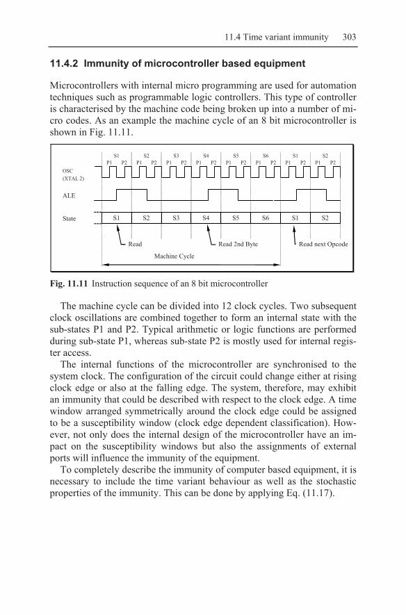
11.4 Time variant immunity 303
11.4.2 Immunity of microcontroller based equipment
Microcontrollers with internal micro programming are used for automation techniques such as programmable logic controllers. This type of controller is characterised by the machine code being broken up into a number of mi-cro codes. As an example the machine cycle of an 8 bit microcontroller is shown in Fig. 11.11.
OSC (XTAL 2)
S1
P1 P2
S2
P1 P2
S3
P1 P2
S4
P1 P2
S5
P1 P2
S6
P1 P2
S1
P1 P2
S2
P1 P2
ALE
S1 S2 S3 S4 S5 S6 S1 S2 State
Read Read next Opcode Read 2nd Byte
Machine Cycle
Fig. 11.11 Instruction sequence of an 8 bit microcontroller
The machine cycle can be divided into 12 clock cycles. Two subsequent clock oscillations are combined together to form an internal state with the sub-states P1 and P2. Typical arithmetic or logic functions are performed during sub-state P1, whereas sub-state P2 is mostly used for internal regis-ter access.
The internal functions of the microcontroller are synchronised to the system clock. The configuration of the circuit could change either at rising clock edge or also at the falling edge. The system, therefore, may exhibit an immunity that could be described with respect to the clock edge. A time window arranged symmetrically around the clock edge could be assigned to be a susceptibility window (clock edge dependent classification). How-ever, not only does the internal design of the microcontroller have an im-pact on the susceptibility windows but also the assignments of external ports will influence the immunity of the equipment.
To completely describe the immunity of computer based equipment, it is necessary to include the time variant behaviour as well as the stochastic properties of the immunity. This can be done by applying Eq. (11.17).

304 11 Model for Immunity Testing
0
0.2
0.4
0.6
0.8
1
1 2 3 4 5 6 7 8 9 10 11 12 13 14 15 16 17 18 19 20 21 22 23 24
Phase within Machine Cycle
Rel
ativ
e Fa
ult F
requ
ency
h t
Command INC A
Command DEC A
Fig. 11.12 Immunity of two complementary machine instructions INC A and
DEC A of a microcontroller as a function of the susceptibility window (50 single EFT spikes in each susceptibility window, amplitude U = 1.25 kV, β = 0.95)
The time scale within the immunity of a microcontroller can change over a large range as depicted by Fig. 11.12.
This example shows the immunity of an 8 bit microcontroller board against single EFT transients coupled via the power lines. The single spikes were synchronously triggered to match the system clock of the board. The system cycle consisting of 12 clock oscillations, i.e. 24 clock edges, was divided into 24 states according to the internal function of the microcontroller.
It can be clearly seen that, at this pulse amplitude, only state 16 can be disturbed. This susceptibility window has a length of only 42 ns at a clock frequency of 12 MHz. According to Fig. 11.12, it can be assumed that the complementary machine instructions are implemented by a micro code, which exhibit similar immunity behaviour.
The determination of the maximum malfunction probability is not pos-sible using state of the art testing procedures. Only the mean malfunction probability can be detected when applying test pulses in a random se-quence. This can be clearly seen when comparing the malfunction prob-abilities of the machine instruction INC A shown in Fig. 11.12 and Fig. 11.13.
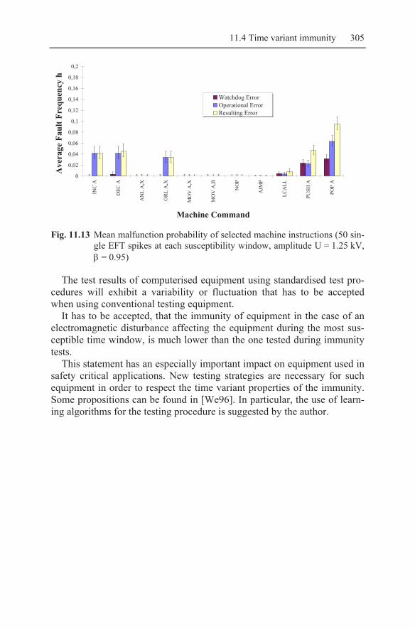
11.4 Time variant immunity 305
0
0,02
0,04
0,06
0,08
0,1
0,12
0,14
0,16
0,18
0,2
INC
A
DEC
A
AN
L A
,X
OR
L A
,X
MO
V A
,X
MO
V A
,B
NO
P
AJM
P
LCA
LL
PUSH
A
POP
A
Machine Command
Ave
rage
Fau
lt Fr
eque
ncy
h
Watchdog Error Operational ErrorResulting Error
Fig. 11.13 Mean malfunction probability of selected machine instructions (50 sin-
gle EFT spikes at each susceptibility window, amplitude U = 1.25 kV, β = 0.95)
The test results of computerised equipment using standardised test pro-cedures will exhibit a variability or fluctuation that has to be accepted when using conventional testing equipment.
It has to be accepted, that the immunity of equipment in the case of an electromagnetic disturbance affecting the equipment during the most sus-ceptible time window, is much lower than the one tested during immunity tests.
This statement has an especially important impact on equipment used in safety critical applications. New testing strategies are necessary for such equipment in order to respect the time variant properties of the immunity. Some propositions can be found in [We96]. In particular, the use of learn-ing algorithms for the testing procedure is suggested by the author.

A1 Electric Fields of Rod Arrangements
In treating electric fields within the scope of EMC, questions often arise about the fields produced by rod arrangements. Naturally in this context, rod arrangements could also be arrangements of wires and conductors. Hence, it is of interest to be able to investigate arbitrary arrangements. A limitation is made in this chapter to parallel rods and wires. Parallel ar-rangements are easy to analyse, general rules and statements can be better evaluated and explained with the aid of parallel arrangements. Currently arbitrary arrangements of thin wires (thin electrodes) are analysed using a computer program, based on the method of moments.
The shielding of electric fields by wire grids (wire meshes) is based on an arrangement of crossing parallel wires, as discussed in chapter 7.2. The first step in analysing this problem is to locate line charges on the axis of the wires, which, for the time being, have an unknown magnitude. After-wards, by using the boundary condition φ = const., the magnitudes are cal-culated. If the location and magnitude of the line charges are known then the fields can be determined.
Electric fields of rod arrangements are of considerable interest if elec-tromagnetic fields of rods or wires have to be approximated in which the electric field component dominates, if the capacitive coupling has to be considered and/or if the capacitances or partial capacitances for subsequent investigations are needed. The following cases can be listed as examples of the necessary or desirable analysis of rod arrangements:
1. Prediction of partial capacitances for the analysis of bundles of ca-bles, and also of cables in general,
2. Shielding effect of grounded wires (See chapter 3.1 for more details), 3. Electromagnetic field of a rod or whip antenna in the vicinity of sys-
tem cables (example in chapter 6.4.3) or with some other secondary radiators are located nearby.
This annex chapter is divided into 3 sub chapters. In A1.1, the principle of potential coefficients and partial capacitances is presented. It is ex-plained in detail by considering infinitively long parallel wires above ground. Then, in A1.2, the arrangement of n parallel horizontal wires is described with the associated equations, which are then applied to an ex-ample. K.-H. Gonschorek, R. Vick, Electromagnetic Compatibility for Device Design and System Integration, DOI 10.1007/978-3-642-03290-5_12, © Springer-Verlag Berlin Heidelberg 2009
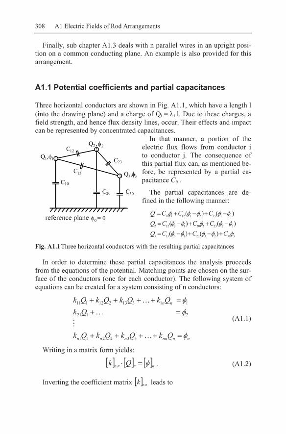
308 A1 Electric Fields of Rod Arrangements
Finally, sub chapter A1.3 deals with n parallel wires in an upright posi-tion on a common conducting plane. An example is also provided for this arrangement.
A1.1 Potential coefficients and partial capacitances
Three horizontal conductors are shown in Fig. A1.1, which have a length l (into the drawing plane) and a charge of Qi = λi l. Due to these charges, a field strength, and hence flux density lines, occur. Their effects and impact can be represented by concentrated capacitances.
In that manner, a portion of the electric flux flows from conductor i to conductor j. The consequence of this partial flux can, as mentioned be-fore, be represented by a partial ca-pacitance Cij .
The partial capacitances are de-fined in the following manner:
330232313133
322322012122
311321121101
)()()()(
)()(
φφφφφφφφφφφφφφφ
CCCQCCCQCCCQ
+−+−=
−++−=
−+−+=
Fig. A1.1 Three horizontal conductors with the resulting partial capacitances
In order to determine these partial capacitances the analysis proceeds from the equations of the potential. Matching points are chosen on the sur-face of the conductors (one for each conductor). The following system of equations can be created for a system consisting of n conductors:
nnnnnnn
nn
QkQkQkQk
QkQkQkQkQk
φ
φφ
=++++
=+=++++
…
……
332211
2121
11313212111
(A1.1)
Writing in a matrix form yields:
[ ] [ ] [ ]nnnn Qk φ=⋅, . (A1.2)
Inverting the coefficient matrix [ ] nnk , leads to

A1.2 Horizontal conductors above ground 309
[ ] [ ] [ ] [ ] [ ]nnnnnnn KkQ φφ ⋅=⋅= −
,1, , (A1.3)
where the coefficients Kij are called the potential coefficients.
The first row, for example, can now be written:
…+++= 3132121111 φφφ KKKQ (A1.4)
The charge Q1 is given by the sum of contributions from all of the po-tentials involved:
…−−⋅−−⋅−⋅⎟⎠⎞⎜
⎝⎛ ∑+=
=)()( 311321121
21111 φφφφφ KKKKQ
n
ii (A1.5)
This equation has the desired form and all partial capacitances can be derived:
∑=∑+===
n
ii
n
ii KKKC
11
211110 , (A1.6)
ii KC 11 −= . (A1.7)
The same definition law has to be applied to all other rows.
A1.2 Horizontal conductors above ground
The following evaluations are valid for infinitely long horizontal conduc-tors above ground. They have been used to create the computer program HCOND, which is described in A1.2.1 and is available on the home page of the authors.
Single conductor arrangement
An infinitely long wire running parallel to a conducting plane (See Fig. A1.2) bears the line charge λi. Therefore, at a field point P(xP,zP), the wire produces a potential of
( ) ( )( ) ( )22
22
ln2
iPip
iPipiP
zzxx
zzxx
−+−
++−⋅=
πελφ (A1.8)
and an electric field strength of zzPxxPPP eEeEzxE ⋅+⋅=),( with

310 A1 Electric Fields of Rod Arrangements
( ) ( ) ⎥⎦⎤
⎢⎣
⎡
++−−
−−+−
−⋅= 2222 )()(2 iPiP
iP
iPiP
iPixP zzxx
xxzzxx
xxEπελ , (A1.9)
( ) ( ) ⎥⎦⎤
⎢⎣
⎡
++−+
−−+−
−⋅= 2222 )()(2 iPiP
iP
iPiP
iPizP zzxx
zzzzxx
zzEπελ . (A1.10)
z
x
r
-
i
i
P(x ,z )
(x ,z )
(x ,-z )
P P
i i
i i
r’
2R
Fig. A1.2 Horizontal conductor above ground
If the potential φi is given, which is normally the case, then as a first step the line charge λi has to be predicted. This can be done by choosing a field point on the surface of the conductor (for instance xp = xi + R, zp = zi) and requiring that the potential has a pre-defined value (value on the conduc-tor), φP = φi. Solving Eq. (A1.8) using the actual geometrical data for the line charge yields
( )R
zR i
iii 22 2
ln2 +
==φ
πελλ .
(A1.11)
Example A1.1: A conductor, 2 m above ground, has a radius of R = 1 cm and a voltage to ground of 100 V (coordinates of the centre axis: xi = 0, zi = 2 m). How large are the potential and electric field strength at the point xp = 1 m, zp = 1 m? What is the value of the capacitance per metre length to ground?
1. According to Eq. (A1.11), the line charge can be determined to be iλ = 16.7 V .

A1.2 Horizontal conductors above ground 311
2. At the field point xP = 1 m, zP = 1 m a potential of Pφ = 13.4 V ac-cording to (A1.8) and an electric field strength of
mVeemmE zx /4.137.6)1,1( ⋅−⋅= according to (A1.10) and (A1.11) are predicted.
3. The capacitance C is calculated using C = Q/U. Hence, it follows that
./3.92' mpFU
C o ==πελ
Two conductor arrangement
]'ln'ln[2
1)(2
22
1
11 r
rrrP ⋅+⋅⋅= λλ
επφ (A1.12)
The conductors have radii 2
1d and 2
2d .
Fig. A1.3 Two conductor arrangement above ground
The partial capacitances are still analytically predictable for the case of two conductors above a conducting ground. A two conductor arrangement is shown in Fig. A1.3. The potential at a field point P is calculated from the superposition of the potentials of two line charges.
The potential on the surface of conductor 1 is given by
],'ln2/
2ln[2
12
1
111 a
ad
h⋅+
⋅⋅⋅= λλ
επφ (A1.13)
],'ln4ln[2
12
1
111 a
aQdhQ
l⋅+⋅⋅=
επφ (A1.14)
and for conductor 2 it is given by
],2/
2ln'ln[2
1
2
2212 d
haa ⋅
⋅+⋅⋅= λλεπ
φ (A1.15)
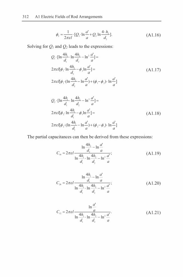
312 A1 Electric Fields of Rod Arrangements
].4ln'ln[2
1
2
2212 d
hQaaQ
l⋅
+⋅⋅=επ
φ (A1.16)
Solving for Q1 and Q2 leads to the expressions:
]'ln)()'ln4(ln[2
]'ln4ln[2
]'ln4ln4[ln
212
21
22
21
2
2
2
1
11
aa
aa
dhl
aa
dhl
aa
dh
dhQ
⋅−+−⋅
=−⋅
=−⋅⋅
φφφεπ
φφεπ
(A1.17)
]'ln)()'ln4(ln[2
]'ln4ln[2
]'ln4ln4[ln
121
12
11
12
2
2
2
1
12
aa
aa
dhl
aa
dhl
aa
dh
dhQ
⋅−+−⋅
=−⋅
=−⋅⋅
φφφεπ
φφεπ
(A1.18)
The partial capacitances can then be derived from these expressions:
;'ln4ln4ln
'ln4ln2
2
2
2
1
1
2
2
10
aa
dh
dh
aa
dh
lC−⋅
−= επ
(A1.19)
;'ln4ln4ln
'ln4ln2
2
2
2
1
1
1
1
20
aa
dh
dh
aa
dh
lC−⋅
−= επ
(A1.20)
.'ln4ln4ln
'ln2
2
2
2
1
112
aa
dh
dh
aa
lC−⋅
= επ
(A1.21)
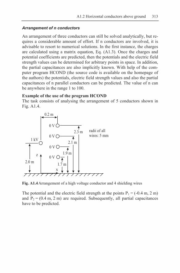
A1.2 Horizontal conductors above ground 313
Arrangement of n conductors
An arrangement of three conductors can still be solved analytically, but re-quires a considerable amount of effort. If n conductors are involved, it is advisable to resort to numerical solutions. In the first instance, the charges are calculated using a matrix equation, Eq. (A1.3). Once the charges and potential coefficients are predicted, then the potentials and the electric field strength values can be determined for arbitrary points in space. In addition, the partial capacitances are also implicitly known. With help of the com-puter program HCOND (the source code is available on the homepage of the authors) the potentials, electric field strength values and also the partial capacitances of n parallel conductors can be predicted. The value of n can be anywhere in the range 1 to 100.
Example of the use of the program HCOND The task consists of analysing the arrangement of 5 conductors shown in Fig. A1.4.
z
x
1 kV0 V
0 V
0 V
0 V
1.7 m
1.9 m
2.1 m
2.3 m radii of all
wires: 5 mm
0.2 m
2.0 m
Fig. A1.4 Arrangement of a high voltage conductor and 4 shielding wires
The potential and the electric field strength at the points P1 = (-0.4 m, 2 m) and P2 = (0.4 m, 2 m) are required. Subsequently, all partial capacitances have to be predicted.

314 A1 Electric Fields of Rod Arrangements
Output data of the program HCOND Arrangement – horizontal conductors
============================
1. Conductor
------------
x-Wert in m = 0
z-Wert in m = 2
Radius in cm = .5
Voltage to ground = 1000
2. conductor
------------
x-Wert in m = .2
z-Wert in m = 1.7
Radius in cm = .5
Voltage to grond = 0
3. conductor
------------
x-Wert in m = .2
z-Wert in m = 1.9
Radius in cm = .5
Voltage to ground = 0
4. Conductor
------------
x-Wert in m = .2
z-Wert in m = 2.1
Radius in cm = .5
Voltage to ground = 0
5. Conductor
------------
x-Wert in m = .2
z-Wert in m = 2.3
Radius in cm = .5
Voltage to ground = 0
1. Field point (-.4 , 2 )
==========================
Potential = 202.5981 V, Ex = -297.5522 V/m, Ez = -13.3946 V/m
2. Field point ( .4 , 2 )
==========================
Potential = 73.30295 V, Ex = 61.25162 V/m, Ez = -9.042034 V/m

A1.3 Vertical conductors above ground 315
Partial capacitances
================
C 1 0 = 3.202583 pF/m
C 1 2 = 1.668292 pF/m
C 1 3 = 2.559265 pF/m
C 1 4 = 2.584133 pF/m
C 1 5 = 1.763822 pF/m
C 2 1 = 1.668292 pF/m
C 2 0 = 4.227483 pF/m
C 2 3 = 3.366044 pF/m
C 2 4 = 1.162033 pF/m
C 2 5 = .8385063 pF/m
C 3 1 = 2.559264 pF/m
C 3 2 = 3.366044 pF/m
C 3 0 = 2.687009 pF/m
C 3 4 = 2.85189 pF/m
C 3 5 = 1.209272 pF/m
C 4 1 = 2.584133 pF/m
C 4 2 = 1.162033 pF/m
C 4 3 = 2.85189 pF/m
C 4 0 = 2.557232 pF/m
C 4 5 = 3.477014 pF/m
C 5 1 = 1.763822 pF/m
C 5 2 = .8385062 pF/m
C 5 3 = 1.209272 pF/m
C 5 4 = 3.477014 pF/m
C 5 0 = 3.728806 pF/m
A1.2.1 Source code of the program HCOND
The source code of the program HCOND (originally HLEITER) is not printed here. It is printed in the German version of the book and available from the homepage of the authors.
A1.3 Vertical conductors above ground
The following evaluations are valid for finitely long vertical conductors that have their lower end in contact with the conducting plane. They have been used to create the computer program VROD.

316 A1 Electric Fields of Rod Arrangements
Arrangement of one wire
r
P(r,z)
z
z2
z1
i
Fig. A1.5 Vertical wire in free space
A finitely long conductor (See Fig. A1.5), which is carrying a line charge λi , produces a potential at the field point P(r, z) equal to
²)²(²)²(
ln4
22
11
rzzzzrzzzz
iP
+−+−
+−+−⋅=
επλφ . (A1.22)
It is also possible to predict the potential of the conductor (line charge) if it is located above a conducting plane, by assuming an additional mirror charge is located below the plane. This results in the potential:
).²)²(
²)²(
²)²(
²)²(ln(
422
11
22
11
rzzzz
rzzzz
rzzzz
rzzzzi
P++++
++++⋅
+−+−
+−+−⋅=
επλφ (A1.23)
For z1 = 0 (end point z1 on ground), the equation simplifies to
).²)²(
²²²)²(
²²ln(4
2222 rzzzzrzz
rzzzzrzz
P++++
++⋅
+−+−++
⋅=επ
λφ (A1.24)
A wire i of length = z2, which is carrying a line charge λi, is located at the point xi, yi. The potential at the field point P (xp, yp, zp) is calculable us-ing the following equation:
).)()()²(
)()(²
)()()²(
)()(ln(
4
2222
22
2222
222
iPipPP
iPipPP
iPipPP
iPipPPiP
yyxxzzzz
yyxxzz
yyxxzzzz
yyxxzz
−+−++++
−+−++
⋅−+−+−+−
−+−++⋅=
επλφ
(A1.25)

A1.3 Vertical conductors above ground 317
The electric field strength on the conducting plane only has a z-component, ( ) zzPPPPP eEzyxE ⋅== 0,, . It can be determined for the wire i using
⎟⎟⎟
⎠
⎞
⎜⎜⎜
⎝
⎛
−+−−
+−+−=
2222
22 )()(2
)()(2
4iPipiPip
izP
yyxxzyyxxE
πελ . (A1.26)
In the usual case the potential φi is given and the line charge λi has to be calculated. This can be done in the following manner: A point is chosen on the surface of the wire (for instance xp = xi + R, yp = yi, zp = z2/2) and it is enforced that the potential at this point must have the value φP = φi. Rear-ranging Eq. (A1.24) for the line large iλ and inserting the corresponding values yields:
)
²2
32
3
²22
²22
²22
ln(
4
222
222
222
222
Rzz
Rzz
Rzz
Rzz
iii
+⎟⎠⎞
⎜⎝⎛+
+⎟⎠⎞
⎜⎝⎛+
⋅
+⎟⎠⎞
⎜⎝⎛+−
+⎟⎠⎞
⎜⎝⎛+
==φ
επλλ .
(A1.27)
Examples where these equations are applied are given in chapter 6.4.3.
Arrangement consisting of n wires
Equations may be found for a direct solution to problems involving two-wire and three-wire arrangements. If n wires are given, it is advisable to resort to numerical solutions, specifically those based on computer calcula-tions. Again, the line charges are initially determined using a matrix equa-tion, Eq. (A1.3). If the line charges and potential coefficients are available, potential and field strength values of arbitrary points in space, and also partial capacitances, can be predicted. With help of the program VROD of chapter A1.3.1 the potentials, field strength values and partial capacitances of n parallel conductors can be investigated. Here, n may be any number between 1 and 100.
Remark: It must be observed when writing such a program that, for finitely long conductors, the total charge has to be calculated from the line charge multiplied by the corresponding length before predicting the poten-tial coefficients via a matrix inversion, see Eq. (A1.2).
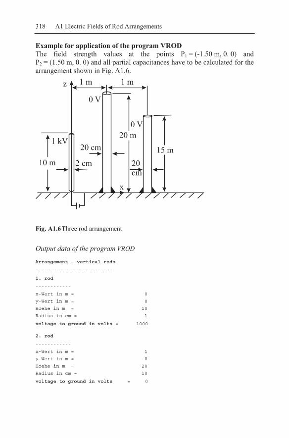
318 A1 Electric Fields of Rod Arrangements
Example for application of the program VROD The field strength values at the points P1 = (-1.50 m, 0. 0) and P2 = (1.50 m, 0. 0) and all partial capacitances have to be calculated for the arrangement shown in Fig. A1.6.
Fig. A1.6 Three rod arrangement
Output data of the program VROD
Arrangement – vertical rods
==========================
1. rod
------------
x-Wert in m = 0
y-Wert in m = 0
Hoehe in m = 10
Radius in cm = 1
voltage to ground in volts = 1000
2. rod
------------
x-Wert in m = 1
y-Wert in m = 0
Hoehe in m = 20
Radius in cm = 10
voltage to ground in volts = 0
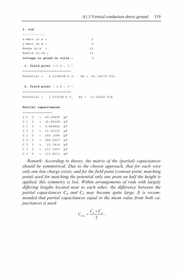
A1.3 Vertical conductors above ground 319
3. rod
------------
x-Wert in m = 2
y-Wert in m = 0
Hoehe in m = 15
Radius in cm = 10
voltage to grond in volts = 0
1. field point (-1.5 , 0 )
==========================
Potential = 2.233862E-6 V, Ez = -81.54079 V/m
2. field point ( 1.5 , 0 )
==========================
Potential = 1.63919E-6 V, Ez = 13.14524 V/m
Partial capacitances
================
C 1 0 = 49.25893 pF
C 1 2 = 36.68308 pF
C 1 3 = 9.964862 pF
C 2 1 = 31.91131 pF
C 2 0 = 140.1084 pF
C 2 3 = 148.6927 pF
C 3 1 = 23.7816 pF
C 3 2 = 111.1667 pF
C 3 0 = 113.8211 pF
Remark: According to theory, the matrix of the (partial) capacitances should be symmetrical. Due to the chosen approach, that for each wire only one line charge exists, and for the field point (contour point, matching point) used for matching the potential only one point on half the height is applied, this symmetry is lost. Within arrangements of rods with largely differing lengths located near to each other, the difference between the partial capacitances Cij and Cji may become quite large. It is recom-mended that partial capacitances equal to the mean value from both ca-pacitances is used:
2jiij
ijneu
CCC
+= .

320 A1 Electric Fields of Rod Arrangements
A1.3.1 Source code of the program VROD
The source code VROD is not printed here. It is given in the German version of the book and is available from the homepage of the authors.

A2 Magnetic Stray Fields
A2.1 Stray field low installation of cables
It was stated in chapter 4.2 that, by using a special installment technique for cables, the magnetic stray field around the cable can be considerably reduced. In order to completely compensate for the field, the return current has to flow along the same route as the forward current. This condition can only be approximately (in theory ideally) achieved by using a coaxial ca-ble. However, this type of cable is not appropriate for use as a power sup-ply cable due to heating reasons. A very good compromise can be achieved by use of a multi sector cable.
The approximation equations for four core arrangements (five core ar-rangements including the single core cable) are derived in this annex chap-ter. It is then shown that the sequence of phases has a decisive influence on the magnitude of the stray field being produced.
A2.1.1 The single core cable (case (a) of chapter 4.2)
By starting with Ampere’s law within Maxwell’s equations, the well-known relation for an infinitely long wire (Fig. A2.1) can be derived,
rIH
⋅⋅=
πϕ 2. (A2.1)
I H
H H
H
I R
Fig. A2.1 Magnetic field around a single core conductor K.-H. Gonschorek, R. Vick, Electromagnetic Compatibility for Device Design and System Integration, DOI 10.1007/978-3-642-03290-5_13, © Springer-Verlag Berlin Heidelberg 2009

322 A2 Magnetic Stray Fields
The assignment of the field vector direction from the current direction is determined by the right screw rule.
A2.1.2 Cable with one forward and one return conductor (case (b) of chapter 4.2)
H H = H
R
d
1
1
2
2
2 1-
Fig. A2.2 Magnetic field of a two conductor cable
Auxiliary calculation:
ε represents a very small value ( )( )
!3sin
311
2112
11
11
1
3
3
2
εεε
εε
εε
εε
εε
−≈
+≈+
+≈+
+≈+
−≈+
( )
⎟⎠⎞
⎜⎝⎛ +−+
⋅⋅≈
⎟⎟⎟⎟
⎠
⎞
⎜⎜⎜⎜
⎝
⎛
+−
−⋅⋅=
⎟⎠⎞
⎜⎝⎛ +⋅⋅
−⎟⎠⎞
⎜⎝⎛ −⋅⋅
=
⎟⎠⎞
⎜⎝⎛ +⋅⋅
−⎟⎠⎞
⎜⎝⎛ −⋅⋅
=
Rd
Rd
RI
Rd
RdR
I
RdR
I
RdR
I
dR
IdR
IRH
21
21
2
21
1
21
12
212
212
22
22
π
πππ
ππ

A2.1 Stray field low installation of cables 323
22)(
RdIRH⋅⋅
⋅≈
π (A2.2)
A2.1.3 Use of two forward- and two return conductors (case (c1) of chapter 4.2)
H
H
H
H
R
d
1
1
2 3 4
234
2
3
1
4
-
-
I/2I/2I/2I/2
Fig. A2.3 Four conductor cable
( ) ( )
⎟⎠⎞
⎜⎝⎛ +−+
⋅⋅⋅
≈⎟⎟⎟⎟
⎠
⎞
⎜⎜⎜⎜
⎝
⎛
+−
−⋅⋅⋅
≈
⎟⎟⎟⎟⎟
⎠
⎞
⎜⎜⎜⎜⎜
⎝
⎛
⎟⎠⎞
⎜⎝⎛ +
−
⎟⎠⎞
⎜⎝⎛ −
⋅⋅⋅
=
+⋅⋅⋅
−−⋅⋅
⋅≈
Rd
Rd
RdI
Rd
RdR
dI
Rd
RdR
dI
dRdI
dRdIH
21212
2/21
121
12
2/
1
1
1
12
2/
22/
22/
22
222
22
ππ
π
ππ
3
2
22/4)(
RdIRH
⋅⋅⋅⋅
≈π (A2.3)
A simple summation of the single parts would have yielded the same re-sult if, in each case, one term more had been considered in the geometric series expansion used in the approximation,

324 A2 Magnetic Stray Fields
211
1 εεε
+−≈+ .
A2.1.4 Installation of the forward and return conductors above a common ground plane (case (c2) of chapter 4.2)
R
d
d/2
3
1
1
4
223
4
x
y
Mirror cable Fig. A2.4 Installation of a two conductor cable above conducting ground
The y-components compensate each other in this case. Therefore, only the x-components have to be considered.
2 1
2 2 2 2
2 12 2 2 2
2 1
2 sin 2 sin
2 22 2 2 2
/ 2 / 2sin , sin
2 2 2 2
sin sin2
x
I IH H
d d d dR R
d d
d d d dR R
dR
α α
π π
α α
α α
⋅ ⋅ ⋅ ⋅= = −
⋅ ⋅ − + ⋅ ⋅ + +
= =
− + + +
≈ ≈
⎛ ⎞ ⎛ ⎞ ⎛ ⎞ ⎛ ⎞⎜ ⎟ ⎜ ⎟ ⎜ ⎟ ⎜ ⎟⎝ ⎠ ⎝ ⎠ ⎝ ⎠ ⎝ ⎠
⎛ ⎞ ⎛ ⎞ ⎛ ⎞ ⎛ ⎞⎜ ⎟ ⎜ ⎟ ⎜ ⎟ ⎜ ⎟⎝ ⎠ ⎝ ⎠ ⎝ ⎠ ⎝ ⎠

A2.1 Stray field low installation of cables 325
⎟⎠
⎞⎜⎝
⎛ +−+⋅⋅
⋅≈
⎟⎟⎟⎟
⎠
⎞
⎜⎜⎜⎜
⎝
⎛
+−
−⋅⋅⋅
≈
⎟⎟⎟⎟⎟
⎠
⎞
⎜⎜⎜⎜⎜
⎝
⎛
+−
−⋅⋅
⋅≈
⎟⎟⎟⎟⎟⎟
⎠
⎞
⎜⎜⎜⎜⎜⎜
⎝
⎛
⎟⎠⎞
⎜⎝⎛+⎟
⎠⎞
⎜⎝⎛ +
−
⎟⎠⎞
⎜⎝⎛+⎟
⎠⎞
⎜⎝⎛ −
⋅⋅⋅
=
Rd
Rd
RdI
Rd
RdR
dI
Rd
RdR
dI
Rd
Rd
Rd
RdR
dIH
21
21
2
21
1
21
12
1
1
1
12
221
1
221
12
2
22
22222
π
ππ
π
3
2
2)(
RdIRH⋅⋅
⋅≈
π (A2.4)
A2.1.5 Use of four forward and four return conductors (case (d) of chapter 4.2)
R
d
I/4
I/4
I/4
I/4
I/4
I/4
I/4
I/4 Fig. A2.5 Eight conductor cable
( ) ( )3
2
3
2
224/4
224/4
dRdI
dRdIH
+⋅⋅⋅⋅
−−⋅⋅⋅⋅
≈ππ

326 A2 Magnetic Stray Fields
⎟⎟⎟⎟
⎠
⎞
⎜⎜⎜⎜
⎝
⎛
+−
−⋅⋅⋅⋅
≈
⎟⎟⎟⎟⎟
⎠
⎞
⎜⎜⎜⎜⎜
⎝
⎛
⎟⎠⎞
⎜⎝⎛ +
−
⎟⎠⎞
⎜⎝⎛ −
⋅⋅⋅⋅
≈
Rd
RdR
dI
Rd
RdR
dIH
61
161
12
4/4
21
121
12
4/4
3
2
333
2
π
π
⎟⎠⎞
⎜⎝⎛ +−+
⋅⋅⋅⋅
≈Rd
Rd
RdI 6161
24/4
3
2
π
4
3
24/48)(R
dIRH⋅⋅
⋅⋅≈
π (A2.5)
From these derivations, three facts can be recognised: 1. Each time the number of cores is doubled, a reduction of the field by
an additional power in the distance law is affected. 2. The cores introduced to double the number of cores have to be ar-
ranged in such way that the phase order in the cores yield an addi-tional compensation.
1/r 1/r 1/r 1/r
1/r
2 3 4
5
3. For 2n-cores (n = 1, 2, 3 ...), the following formula can be stated:
∏⋅⋅⋅⋅
⋅≈
=
−
+
− n
i
in
nn
nR
dI
RH1
11
1
2!22)(
π (A2.6)

A2.2 Computer program for predicting magnetic stray fields 327
A2.2 Computer program for predicting magnetic stray fields
A2.2.1 Field of a finitely long wire
Assuming that the current in a wire is taken to be flowing as a concen-trated region on the wire’s axis, then the magnetic field strength at an arbi-trary field point outside the wire can be predicted using the Biot-Savart law:
,4 3s
sxldIHl∫=
π (A2.7)
s = vector from the source element I dl to the field point, s = | s |.
The underlining of I and H points to the fact that both quantities may be complex. The phase dependence of the current is transferred into a phase dependence of the magnetic field strength.
Consider a finitely long straight wire, positioned on the y-axis, bearing the current I and extending from y = 0 to y = a (See Fig. A2.6). Given this arrangement, the following equation for a field point in the xy-plane (z = 0) can be derived:
.))(
(4 2222 ze
yxxy
ayxxayIH
+−
−+
−=
π (A2.8)
z
a
y
x
P(x,y,0)
I
Fig. A2.6 Finitely long wire on the y-axis, carrying the current I

328 A2 Magnetic Stray Fields
The derivation is elementary. If the wire is located arbitrarily in space (See Fig. A2.7), a matched coordinate system (x,y,z) can be found whereby the assumptions used in Eq. (A2.8) are fulfilled.
z
z y
x
P
P
P
1
1
0
0
y
x
r
r
r
I
Fig. A2.7 Finitely long wire located arbitrarily in space, carrying the current I
Eq. (A2.8) can be rewritten to yield Eq. (A2.9):
ze
yxx
y
ayxx
ayIH ))(
(4 2222
+−
−+
−=
π (A2.9)
The quantities with lines above in this equation can be determined through the following vector relations:
1. The field point P(x, y, z) must lie in the yx, -plane of the matched coordinate system. The unit vector
ze of this plane has to be pre-
dicted. To do so, the directed area spanned by the vector ( orr − ) and ( orr −1 ) must be determined and then divided by its magnitude (its absolute value),
|)()(|)()(
1
1
oo
ooz rrxrr
rrxrre−−−−
= . (A2.10)
2. a is the length of the vector ( 1 or r− ). The consequence of the direc-tion of this vector is considered in Eq. (A2.10). Therefore, this quan-tity is considered within the unit vector
ze ,
|| 1 orra −= . (A2.11)

A2.2 Computer program for predicting magnetic stray fields 329
3. The x -coordinate of the field point is obtained by predicting again the area spanned by the vectors ( orr − ) and ( orr −1 ). This is then di-vided by the distance | orr −1 | to yield the required result. The area spanned by the vectors is, in the general case, a trapezium with an area calculated as the base line multiplied by the height,
|||)r)x( r-r(|
1
1o
o
o
rrrx
−−
= . (A2.12)
4. The missing coordinate y is the distance (directed, positive or nega-tive) between the orthogonally projected point of P ( zyx ,, ) onto the y -axis and the origin of the coordinate system ( zyx ,, ),
||)r() r-r(
1
1o
o
o
rrry
−−⋅
= . (A2.13)
As orr , and 1r are defined in the global coordinate system, it is possible to predict the magnetic field strength of a finitely long straight wire located arbitrarily in space by using the preceding relations in the global coordi-nate system.
The total field of an arbitrary arrangement of N wires with the currents Ii can be calculated from the phase and vector addition of each individual part. This task should be performed using a computer.
It has been assumed that all curved, non-straight, wire courses can be rebuilt using polygons.
A2.2.2 Field of a single layered coil
The derivations in the preceding chapter are elementary. In addition, the calculation of the magnetic field of a single layered coil is more a geomet-rical than an electrical problem. Therefore, the relations for the rebuilding of coil windings by a system of polygons are briefly derived here; see also Fig. A2.8.

330 A2 Magnetic Stray Fields
a) b)z z
yy
xx
R R0
Fig. A2.8 Rebuilding of a coil by a polygon
Consider a coil with the coordinates xA, yA, zA and xE, yE, zE for the starting and ending points of its center axis respectively. The coil has a ra-dius of Ro. Using these parameters, the straight line of the center axis can be written as a vector in the following manner:
, , , , ( , , ),0 1.
A A A E A E A E Ax y z x y z t x x y y z zt
= + − − −≤ ≤
(A2.14)
Should the reader wish to rebuild one winding by N finite straight lines (See Fig. A2.8), where the coil has a total of M windings, then the end point of the i-th straight line has the following axis coordinates:
, , , , ( , , ),
1 .
i i i A A A E A E A E A
ix y z x y z x x y y z z
MNi MN
= + − − −
≤ ≤
(A2.15)
The individual end points are located on a circle of radius R, positioned around the centre axis, within planes perpendicular to the axis.
The planes containing the end points have the following properties:
They contain the point xi, yi, zi and have the unit vector given by
.)()()(
)(),(),(222
AEAEAE
AEAEAEE
zzyyxxzzyyxxe−+−+−
−−−= (A2.16)
One of these planes, for instance, is defined using a parameter represen-tation by:

A2.2 Computer program for predicting magnetic stray fields 331
,,,,, btaszyxzyx ++= ΡΡΡ (A2.17)
where a and b are two vectors in the plane and are orthogonal to each other. Therefore, the normal vector of the plane is given by the following equation:
.bxan = (A2.18)
As the starting point of the coil winding is not yet fixed, there exists some degree of freedom with relation to the choice of a and b . If some degree of arbitrariness is allowed for the first starting point, then an ap-proach where the inner vector product of Ee and a becomes zero can be used for the further fixings.
This assumption leads (using some abbreviations) to
.0,,,
=++⇒−=−=−=
aaa
AE
AE
AE
CzByAxzzCyyBxxA
(A2.19)
Choosing xa = 1 and ya = 1 (arbitrary), then one obtains
CBAza
+−= ,
and the vector a :
).,1,1(C
BAa +−= (A2.20)
The choice xa = 1 and ya = 1 is not allowed for zE - zA = 0, i.e. the case where the coils have no z-direction.
The vector b must be orientated perpendicular to Ee and is allowed to be located perpendicularly to a . Therefore, it follows
,Eeab ×= (A2.21)
).,,(22
ABCC
BAAC
BBACb −−⋅+
−+⋅
+= (A2.22)
Hence, the planes bearing the end points of the rebuilding straight lines have the following description:

332 A2 Magnetic Stray Fields
,,,,, bsatzyxzyx iii ⋅+⋅+= (A2.23)
with xi, yi, zi as the vector of the projection from end point i onto the coil axis.
One requirement, which has not yet been considered, consists of the fact that the distance between an end point and its projection onto the coil axis has to be equal to the radius R.
This condition can be fulfilled by normalising the vectors a and b to unit vectors and the dependence between t and s is fixed in the following way:
,22 tRs −= Rt ≤ . (A2.24)
Choosing
NiRs π2cos= , (A2.25)
and
NiRt π2sin= (A2.26)
fulfils the additional requirement whereby the end points of the rebuilding straight lines are located on circles with the radius R, and a difference in angle of 360°/N exists between two consecutive end points.
The starting point of the first rebuilding straight line is obtained if, in the preceding equations, a value of i = 0 is chosen.
If, for instance, a coil on the z-axis is being considered, which has a length of 1.2 m, 2 windings and a radius of 1 m, then the starting point of the polygon has the coordinates
)0,1,1(2
,, 111
Rzyx AAA = (A2.27)
and the end point of the first rebuilding straight line has the coordinates
)05.0;285.0;966.0(,, 111 ⋅= Rzyx EEE , (A2.28)
where 12 straight lines have been used to rebuild one winding.
The starting point of the 2nd straight line is given by the end point of the first one.
From inspection of the result of this example it can be observed that the coil has a counter-clockwise turn direction, i.e. the turn direction of a left
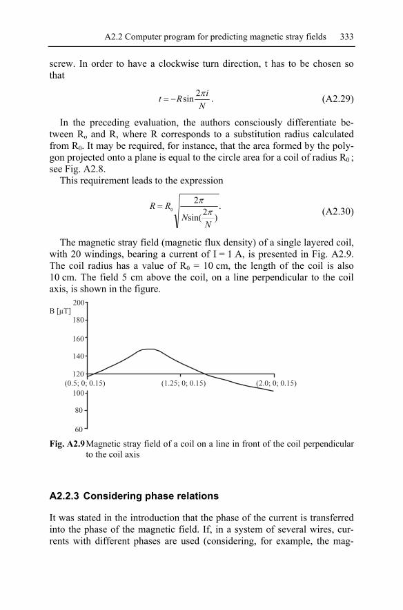
A2.2 Computer program for predicting magnetic stray fields 333
screw. In order to have a clockwise turn direction, t has to be chosen so that
NiRt π2sin−= . (A2.29)
In the preceding evaluation, the authors consciously differentiate be-tween Ro and R, where R corresponds to a substitution radius calculated from R0. It may be required, for instance, that the area formed by the poly-gon projected onto a plane is equal to the circle area for a coil of radius R0 ; see Fig. A2.8.
This requirement leads to the expression
.)2sin(
20
NN
RRπ
π= (A2.30)
The magnetic stray field (magnetic flux density) of a single layered coil, with 20 windings, bearing a current of I = 1 A, is presented in Fig. A2.9. The coil radius has a value of R0 = 10 cm, the length of the coil is also 10 cm. The field 5 cm above the coil, on a line perpendicular to the coil axis, is shown in the figure.
Fig. A2.9 Magnetic stray field of a coil on a line in front of the coil perpendicular
to the coil axis
A2.2.3 Considering phase relations
It was stated in the introduction that the phase of the current is transferred into the phase of the magnetic field. If, in a system of several wires, cur-rents with different phases are used (considering, for example, the mag-

334 A2 Magnetic Stray Fields
netic field of a three phase power supply) a result in the following form is obtained in the general case:
.zzgesyygesxxgesges eHeHeHH ++= (A2.31)
The question then arises: what is the maximum amplitude of this mag-netic field? In order to predict this maximum amplitude, it is not sufficient to extract the root of the squared amounts (absolute values) for each indi-vidual component.
In reality, the real time dependent field in each spatial direction has to be firstly determined from the complex components (real part, imaginary part) of this spatial component. As the second step, via an addition of all squared time dependent spatial components, followed by a square root op-eration, the maximum value can be predicted. For more details the reader is referred to annex chapter A5.
It is assumed that the components in each of the spatial directions are given by the following quantities:
zjzjzzges
yjyjyyges
xjxjxxges
CeeHH
BeeHH
AeeHH
ϕϕ
ϕϕ
ϕϕ
==
==
==
. (A2.32)
From these assumptions, the time dependent values are derived using
)cos()(
)cos()()cos()(
zz
yy
xx
tCtH
tBtHtAtH
ϕω
ϕωϕω
+=
+=
+=
, (A2.33)
leading to
.)22cos(²
)22cos(²)22cos(²²²²2
1
)()()(|| 222
z
yx
zyxges
tC
tBtACBA
tHtHtHH
ϕω
ϕωϕω
++
++++++=
=++=
(A2.34)
This equation is simplified by firstly combining the first two cos-terms, so that:
),2sin(²)22cos(²)22cos(²
D
yx
tDtBtA
ϕω
ϕωϕω
+=
+++ (A2.35)
A2.2 Computer program for predicting magnetic stray fields 335
with
)22cos(2 22442xyBABAD ϕϕ −++= ,
.2sin²2sin²2cos²2cos²
arctanyx
yxD BA
BAϕϕϕϕ
ϕ−−
+=
The result of this substitution is then added to the third cos-term, yield-ing the result:
),2sin(²)2
22sin(²)2sin(² EzD tEtCtD ϕωπϕωϕω +=++++ (A2.36)
with
)2
2cos(2 22442DzCDCDE ϕπϕ −+++= ,
.)
22cos(²sin²
)2
2sin(²sin²arctan
πϕϕ
πϕϕϕ
++
++=
zD
zD
E
CD
CD
As a reminder: The addition of two sinusoidal quantities yields
),sin()sin()sin( 2211 ϕωϕωϕω +=+++ tAtAtA (A2.37)
)cos(2 122122
21 ϕϕ −++= AAAAA
.coscossinsinarctan
2211
2211
ϕϕϕϕϕ
AAAA
++
=
STRAF is a very efficient program, which predicts the magnetic flux densities of a nearly arbitrary arrangement of thin wires.
A2.2.4 Source code of the program STRAYF
The source code SFELD or STRAYF is not reprinted here. It is given in the German version of the book and is available from the homepage of the authors.

A3 Self and Mutual Inductances
A method for predicting magnetic stray fields has been described in annex chapter A2. If the voltage induced into a loop due to this stray field has to be obtained, then Faraday’s law can be applied,
.dtdui
φ−= (A3.1)
where φ is the magnetic flux, which can be calculated using the expression
AdHA∫μ=φ . (A3.2)
Dividing the modulus of the flux, |φ|, by the field producing current, i, yields a quantity M, which is dependent only on the geometry. M is re-ferred to as the mutual inductance. For the sake of completeness, it has to be mentioned that the division
iM || φ
= (A3.3)
is only allowed for regions where no current is flowing (in the process of determining the mutual inductance). This condition is satisfied within all following evaluations. Furthermore, it should be mentioned that the self inductance is only a sub-fraction of the mutual inductance. In the calcula-tion of the self inductance, the area enclosed by the wire, which is carrying the field producing current, is used for calculating the effective flux.
The following statements and equations are taken from the publication GON82.
A3.1 Mutual inductance between a finitely long conductor on the y-axis and a trapezoidal area in the xy-plane
The following equation has already been given in annex chapter A2 for predicting the magnetic stray field in the xy-plane, produced by a finitely long wire on the y-axis:
K.-H. Gonschorek, R. Vick, Electromagnetic Compatibility for Device Design and System Integration, DOI 10.1007/978-3-642-03290-5_14, © Springer-Verlag Berlin Heidelberg 2009

338 A3 Self and Mutual Inductances
.)²²)²(²
(4 ze
yxxy
ayxxayIH
+−
−+
−=
π (A3.4)
The underlining of H and I is neglected here, as they do not have mean-ing in the following evaluations.
It is clear from Eq. (A3.4) that a current on the y-axis produces a field in the xy-plane, which only has a z-component. If the area being influenced is located only in the xy-plane (unit vector ze ), the inner vector product of Eq. (A3.2) reduces to a simple multiplication.
Fig. A3.1 Arrangement consisting of a current carrying conductor on the y-axis
and a trapezoidal area in the xy-plane
Consider a trapezoidal area in the xy-plane, with a current on the y-axis, as shown in Fig. A3.1. In order to predict the mutual inductance, only the following integral has to be solved:
.)²²)²(²
(4
22
11
dxdyyxx
yayxx
ayMbxm
bxm
d
c +−
−+−μ
= ∫∫+
+π (A3.5)
Integration along y yields the following solution:

A3.1 Mutual inductance between a finitely long conductor and xy-plane 339
.²²1²²1 22
11
22
11
bxm
bxm
abxm
abxmy yx
xyx
xI
+
+
−+
−+⎥⎦⎤
⎢⎣⎡ +−⎥⎦
⎤⎢⎣⎡ +=
(A3.6)
Inserting this solution into Eq. (A3.5) leads to integrals of the form
.²1∫ ++= dxgfxex
xI x (A3.7)
Finally, the integrations provide the mutual inductance of an arrange-ment consisting of a straight, finitely long wire on the y-axis and a trape-zoidal area in the xy-plane.
( ) ( ) ( ) ( ) ( ) ( )
( ) ( ) ( ) ( ) ( ) ( )
( ) ( )( ) ( )( ) ( ) ( ) ( ) ( )( ) ( ) ( )
( ) ( ) ( ) ( )( ) ( ) ( )
( ) ( ) ( ) ( ) ( )( ) ( ) ( )
( ) ( ) ( ) ( )( ) ( ) ( )
( ) ( )( ) ( )( ) ( )( ) ( )( ) ( )( ) ( )( ) ( )( ) ( )( ) ( ) ( ) ( )( ) ( ) ( )
( ) ( ) ( ) ( )( ) ( ) ( )
( ) ( ) ( ) ( )( ) ( ) ( )
( ) ( ) ( ) ( )( ) ( ) ( )
( )( )( )( )( )( )( )( ) ⎟
⎟⎟⎟
⎠
⎞
⎟⎠⎞
⎜⎝⎛ +++++
⎟⎠⎞
⎜⎝⎛ +++++
+
⎟⎠⎞
⎜⎝⎛ +++++
⎟⎠⎞
⎜⎝⎛ +++++
+
⎟⎠⎞
⎜⎝⎛ −+−+−+−++−
⎟⎠⎞
⎜⎝⎛ −+−+−+−++−
−+
⎟⎠⎞
⎜⎝⎛ −+−+−+−++−
⎟⎠⎞
⎜⎝⎛ −+−+−+−++−
−+
+++++++
+++++++
++
+++++++
+++++++
++
−+++−+−+++
−+++−+−+++
+
−+
−+++−+−+++
−+++−+−+++
+
−+
+++−++++
+++++++−
−+−+++−+−++−
⎜⎝⎛ −+−++−−+−++
=
dbmbbdbmdmbc
cbmbbcbmcmbdb
cbmbbcbmcmbd
dbmbbdbmdmbcb
cabmababcabmcmabd
dabmababdabmdmabcab
dabmababdabmdmabc
cabmababcabmcmabdab
bmcmbcbmcmm
bmdmbdbmdmm
m
bm
bmdmbdbmdmm
bmcmbcbmcmm
m
bm
abmdmabdabmdmm
abmcmabcabmcmm
m
abm
abmcmabcabmcmm
abmdmabdabmdmm
m
abm
bcbmcmbdbmdm
bcbmcmbdbmdm
abcabmcmabdabmdm
abcabmcmabdabmdm
M
1121
2111
221
21
1121
2111
221
21
1
2222
2222
222
22
2222
2222
222
22
2
112
12
11122
12
1
112
12
11122
12
11
222
22
22222
22
2
222
22
22222
22
22
1121
2111
221
21
1121
2111
221
21
21
11
2222
2222
222
22
2222
2222
222
22
22
22
1121
2111
221
21
1121
2111
221
21
21
11
2222
2222
222
22
2222
2222
222
22
22
22
2111
221
2111
221
2222
222
2222
222
2111
221
2111
221
2222
222
2222
222
21
21ln
21
21ln
21
21ln
21
21ln
1211
1211ln
1
1211
1211ln
1
1211
1211ln
1
1211
1211ln
1
2121
2121
2121
21214πμ
(A3.8)

340 A3 Self and Mutual Inductances
A3.2 Decomposition of an area in the xy-plane bounded by straight lines
Further to the consideration of an arrangement consisting of a finitely long conductor on the y-axis and a trapezoidal area in the xy-plane, as discussed above, it follows that we can calculate the result for an arbitrary area in the xy-plane, limited (bounded) by straight lines. Through decomposition of the complete area into triangles, with one side in parallel to the y-axis (special case of a trapezoidal area), it is possible to obtain a correct ana-lytical solution. An arrangement consisting of an irregular pentagon with its possible triangular decomposition is presented in Fig. A3.2. The total mutual inductance is calculated as the sum of each individual inductance that occurs between the conductor on the y-axis and the six triangles.
y
x
P
P
P
P
P5
4
3
2
1I
I
II
II
IIIIII
a
a
a
b
b
b
Fig. A3.2 Triangular decomposition of an irregular pentagon for predicting the
mutual inductance
The decomposition presented above is, as can be easily seen, not the only one possible. This decomposition requires a lot of checks regarding the relative position of the corner points of the areas with respect to each other, and is therefore badly suited to automation within a computer pro-gram. On the other hand, if the amount |φ12|/i1, according to Eq. (A3.3), is calculated as the last step in the procedure after all subparts, Δφi/ii, of the total arrangement are predicted, then, in intermediate steps, the direction of the area’s normal vector with relation to the magnetic field strength can be used to determine the signs of the subparts. If the area in Fig. A3.2 is de-composed into triangles, as shown in Fig. A3.3, then it can be seen that the triangle I and II have another area orientation compared to triangle III. The

A3.3 Mutual inductance between a finitely long conductor and xy-plane 341
total area of the pentagon is equal to the area of the two triangle I and II, minus that of triangle III.
y
x
P
P
P
P4
3
2
1
P5
I
II
III
Fig. A3.3 Decomposition of an irregular pentagon into triangle areas containing all
the point P1
As H has the same direction in the whole of the xy-plane, the orienta-tion of the influenced area determines the sign of the magnetic flux. For the case presented here, it follows
IIIIIIges φφφφ −+= . (A3.9)
To obtain a definite decomposition, the orientation is chosen in the fol-lowing way: Triangles are formed, one at a time, from the points P1, Pk and Pk + 1 (k = 2,3,..., N-1; N number of corner points). Then, the normal vector of the area is defined as positive if, with increasing index (1, k, k+1), the area is circulated in a mathematically positive sense. This decomposition is unique in that it also allows crossing points of the bounding straight wires to occur.
A3.3 Treatment of arbitrary conductor loops in space
Assume that the wire producing the field is located on the y-axis, using a coordinate transformation, the next step for handling conductor loops in space consists of transforming the influenced loop, in a correct manner, into the xy-plane. The correct procedure, as can be proven easily, involves
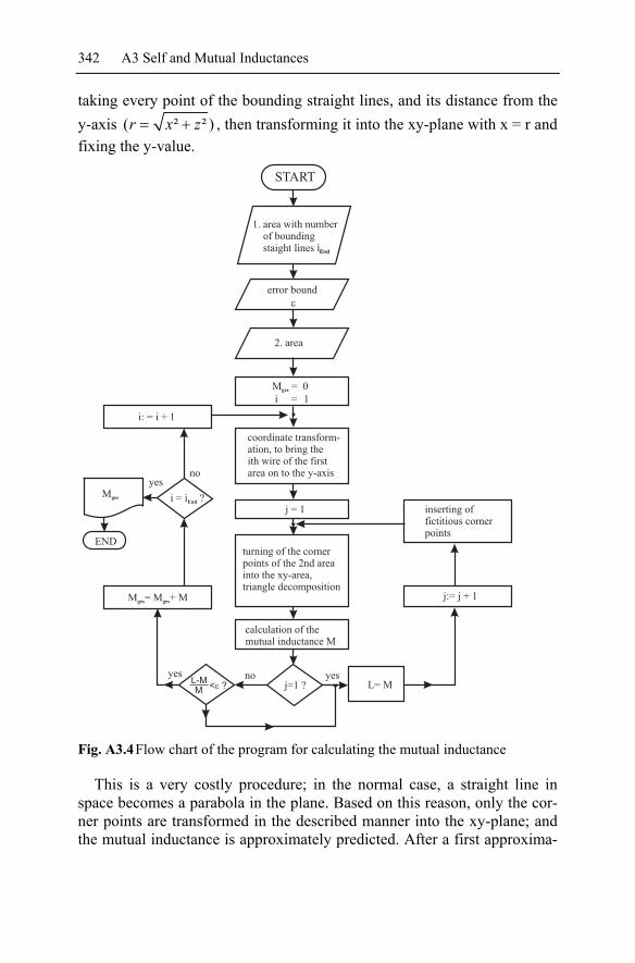
342 A3 Self and Mutual Inductances
taking every point of the bounding straight lines, and its distance from the y-axis ( ² ² )r x z= + , then transforming it into the xy-plane with x = r and fixing the y-value.
Fig. A3.4 Flow chart of the program for calculating the mutual inductance
This is a very costly procedure; in the normal case, a straight line in space becomes a parabola in the plane. Based on this reason, only the cor-ner points are transformed in the described manner into the xy-plane; and the mutual inductance is approximately predicted. After a first approxima-
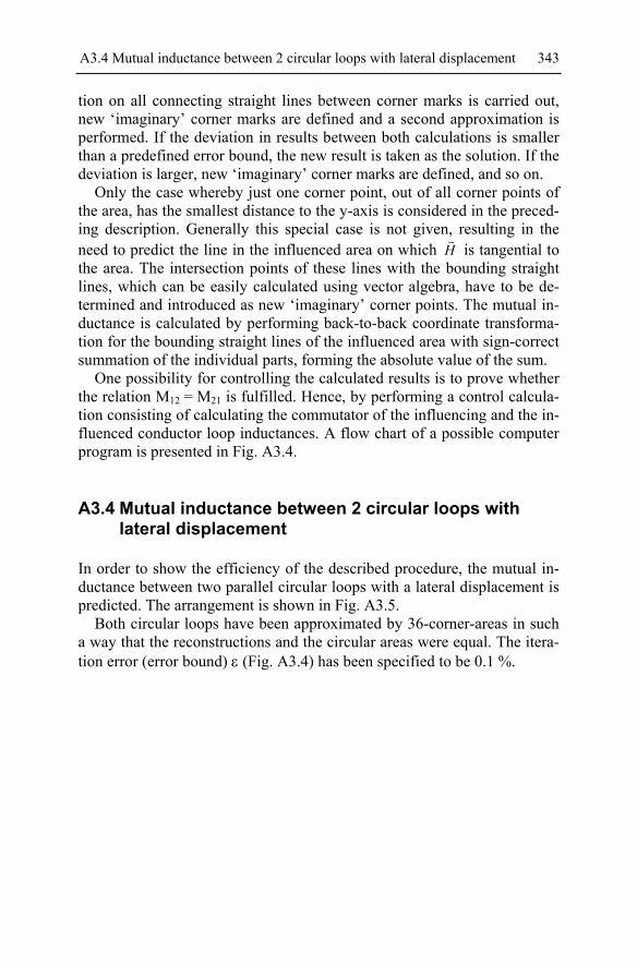
A3.4 Mutual inductance between 2 circular loops with lateral displacement 343
tion on all connecting straight lines between corner marks is carried out, new ‘imaginary’ corner marks are defined and a second approximation is performed. If the deviation in results between both calculations is smaller than a predefined error bound, the new result is taken as the solution. If the deviation is larger, new ‘imaginary’ corner marks are defined, and so on.
Only the case whereby just one corner point, out of all corner points of the area, has the smallest distance to the y-axis is considered in the preced-ing description. Generally this special case is not given, resulting in the need to predict the line in the influenced area on which H is tangential to the area. The intersection points of these lines with the bounding straight lines, which can be easily calculated using vector algebra, have to be de-termined and introduced as new ‘imaginary’ corner points. The mutual in-ductance is calculated by performing back-to-back coordinate transforma-tion for the bounding straight lines of the influenced area with sign-correct summation of the individual parts, forming the absolute value of the sum.
One possibility for controlling the calculated results is to prove whether the relation M12 = M21 is fulfilled. Hence, by performing a control calcula-tion consisting of calculating the commutator of the influencing and the in-fluenced conductor loop inductances. A flow chart of a possible computer program is presented in Fig. A3.4.
A3.4 Mutual inductance between 2 circular loops with lateral displacement
In order to show the efficiency of the described procedure, the mutual in-ductance between two parallel circular loops with a lateral displacement is predicted. The arrangement is shown in Fig. A3.5.
Both circular loops have been approximated by 36-corner-areas in such a way that the reconstructions and the circular areas were equal. The itera-tion error (error bound) ε (Fig. A3.4) has been specified to be 0.1 %.

344 A3 Self and Mutual Inductances
h
x
R
R
y
x
d
z
Fig. A3.5 Arrangement of two laterally displaced circular loops with the same area
and orientation
The mutual inductance for the arrangement of Fig. A3.5, as function of the lateral displacement d, is presented in Fig. A3.6. The different curves correspond to varied heights h between both conductor planes.
d [cm]
0 1 2 3 4 5 6 7 8 9 10 11 12 13 14 15
M
[nH]
500
200
100
50
20
10
5
2
1
0.5
0.2
0.1
h = 1 mm
h = 4 mm
h = 16 mm
h = 32 mm
h = 64 mm
1 k
Fig. A3.6 Mutual inductance between two parallel circular loops
The maximum coupling between both loops is obtained for d=0 in every case. This coupling decreases with lateral displacement, up to a value of zero, and then increases again, up to a local maximum. Starting at this lo-cal maximum, the mutual inductance smoothly decreases again towards a value of zero at d → ∞. Both the first null, as well as the local maximum, are functions of the height h between both loop planes.

A3.5 Source code of the program MUTUAL 345
A3.5 Source code of the program MUTUAL
The source code GEGEN or MUTUAL is not printed here. It is printed in the German version of the book and is available from the homepage of the authors.
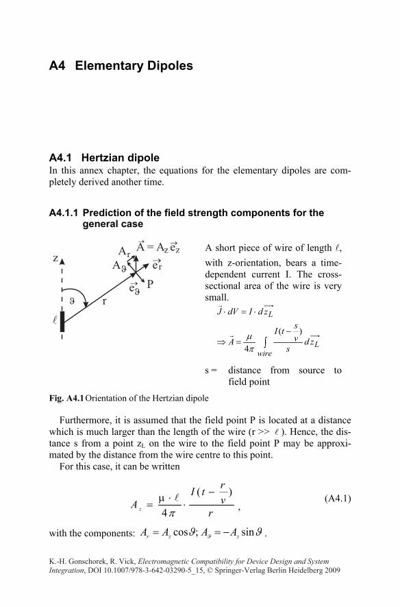
A4 Elementary Dipoles
A4.1 Hertzian dipole In this annex chapter, the equations for the elementary dipoles are com-pletely derived another time.
A4.1.1 Prediction of the field strength components for the general case
A short piece of wire of length , with z-orientation, bears a time-dependent current I. The cross-sectional area of the wire is very small.
∫−
=⇒
⋅=⋅
wireL
L
zds
vstI
A
zdIdVJ
)(
4πμ
s = distance from source to field point
Fig. A4.1 Orientation of the Hertzian dipole
Furthermore, it is assumed that the field point P is located at a distance which is much larger than the length of the wire (r >> ). Hence, the dis-tance s from a point zL on the wire to the field point P may be approxi-mated by the distance from the wire centre to this point.
For this case, it can be written
rvrtI
A z
)(
4
−⋅
⋅μ=
π , (A4.1)
with the components: ϑϑ ϑ sin;cos zzr AAAA −== .
K.-H. Gonschorek, R. Vick, Electromagnetic Compatibility for Device Design and System Integration, DOI 10.1007/978-3-642-03290-5_15, © Springer-Verlag Berlin Heidelberg 2009

348 A4 Elementary Dipoles
The magnetic field strength can be immediately determined from the vector potential
→
A :
1 1 (sin ) 0,sin
1 1 sin ( ) 0,sin
1 1 ( )
1 1( ) sin ( ) sin4
(
4
r r
r
r
AH rot A Ar
AH rot A r Ar r
AH rot A r Ar rr rI t I t
r v v v r
I
r
ϑϕ
ϑ ϑ ϕ
ϕ ϕ ϑ
∂ ∂ϑϑ ∂ϑ ∂ϕ
∂ ∂ϑϑ ∂ϕ ∂
∂ ∂∂ ∂ϑ
ϑ ϑπ
π
→
→
→
⎡ ⎤= ⋅ = ⋅ ⋅ − =⎢ ⎥μ μ ⋅ ⋅ ⎣ ⎦
⎡ ⎤= ⋅ ⋅ = ⋅ − ⋅ ⋅ =⎢ ⎥μ μ ⋅ ⋅ ⎣ ⎦
⎡ ⎤= ⋅ = ⋅ − =⎢ ⎥μ μ ⋅ ⋅ ⎣ ⎦μ ⋅ ⎡ ⎤= + − ⋅ ⋅ + − ⋅ ⋅⎢ ⎥μ ⋅ ⎣ ⎦
= +) ( )
sin .
r rt I tv v
v rϑ
⎡ ⎤− −⎢ ⎥+ ⋅⎢ ⎥
⎢ ⎥⎣ ⎦
(A4.2)
The components Hr and Hϑ are zero because, on one hand, no compo-
nent Aϕ exists and, on the other hand, →
A is not dependent on ϕ. The elec-tric field strength E can be calculated from the magnetic field strength Hϕ, either by considering the auxiliary condition
012
=⋅+→
φv
Adiv , (A4.3)
leading to the potential φ. Alternatively the 1st Maxwell equation can be used.
Here the latter method mentioned is applied:
2
2 2
,
( ) ( )1 (sin ) cos ,sin 2
( ) ( ) ( )1 1 ( ) sin ,sin 4
1 ( )
r
r
r
E rot Hr rI t I tH v vE H
r r v r
r r rI t I t I tH v v vE r Hr r r v rv r
HE r Hr r
ϑϕ
ϑ ϕ
ϕ ϑ
ε
∂ ∂ε ϑ ϑϑ ∂ϑ ∂ϕ π
∂ ∂ε ϑϑ ∂ϕ ∂ π
∂ ∂ε∂ ∂ϑ
→ →
=
⎡ ⎤− −⎢ ⎥⎡ ⎤= ⋅ − = ⋅ + ⋅⎢ ⎥⎢ ⎥
⎣ ⎦ ⎢ ⎥⎣ ⎦
⎡ ⎤− − −⎢ ⎥⎡ ⎤= ⋅ − ⋅ = ⋅ + + ⋅⎢ ⎥⎢ ⎥
⎣ ⎦ ⎢ ⎥⎣ ⎦
⎡= ⋅ −⎢⎣0.⎤ =⎥⎦
(A4.4)

A4.1 Hertzian dipole 349
A4.1.2 Solution for time harmonic excitation
.cosˆ)ˆRe()Re()( tIeIItI tj ωω ⋅=⋅== (A4.5)
Wavelength:
2v vc
πλω
= = .
( )
2
( )
2
( )
2 2
ˆ( 1 ) s in ,
4
ˆ 1 1( ) c o s ,2
ˆ 1 1( ) s in .4
rj tv
rj tv
r
rj tv
I e j rHr v
I eEr v j r
I e j rEr v v j r
ω
ϕ
ω
ω
ϑ
ω ϑπ
ϑπ ε ω
ω ϑπ ε ω
−
−
−
⋅= ⋅ ⋅ + ⋅
⋅= ⋅ ⋅ + ⋅
⋅= ⋅ ⋅ + + ⋅
(A4.6)
Ratio between Εϑ and Ηϕ
2
0
1 1ˆ 1ˆ
1
212 .
12
W
j rE vv v j r
j r vHv
rj jrj
r
ϑ
ϕ
ωω
ωε
λ ππ λ
λπ
+ += ⋅ ⋅
+
− += Γ ⋅ = Γ
+
(A4.7)
Real parts of the field strength components:
2
22
ˆ 2( ) sin( ( )) cos( ( )) sin4ˆ
sin( ( )) ( ) cos( ( )) sin ,2 2
I r r rH t t tr v v
I r rt tr v r v
ϕπ ω ω ϑ
π λ
π λ λω ω ϑλ π π
⋅ ⎡ ⎤= − ⋅ − + − ⋅⎢ ⎥⎣ ⎦
⋅ ⋅ −⎡ ⎤= ⋅ − + ⋅ − ⋅⎢ ⎥⎣ ⎦
(A4.8)

350 A4 Elementary Dipoles
2
2 3
2 32
ˆ 1 1( ) cos( ( )) sin( ( )) cos2ˆ 2 cos( ( )) sin( ( )) cos
4ˆ2 ( ) cos( ( )) ( ) sin( ( )) cos .
2 2
rI r rE t t t
r v v r v
I r r rt tr v v
I r rt tr v r v
ω ω ϑπε ω
λ π ω ω ϑπ ε λ
π λ λω ω ϑλ ε π π
⋅ ⎡ ⎤= ⋅ ⋅ − + ⋅ − ⋅⎢ ⎥⎣ ⎦
⋅ ⋅ μ ⎡ ⎤= ⋅ ⋅ − + − ⋅⎢ ⎥⋅ ⎣ ⎦
⋅ ⋅ ⋅ μ ⎡ ⎤= ⋅ ⋅ − + ⋅ − ⋅⎢ ⎥⎣ ⎦
(A4.9)
2 2
22 3
3 22
ˆ 1 1( ) ( ) sin( ( )) cos( ( )) sin4ˆ 2 21 ( ) sin( ( )) cos( ( )) sin8ˆ
( ) sin( ( )) ( ) cos( (2 2 2
I r r rE t t tr v r v v v
I r r r rt tr v v
I rt tr r v r
ϑω ω ω ϑ
πε ω
λ π πω ω ϑπ ε λ λ
π λ λ λω ωλ ε π π π
⋅ ⎡ ⎤= ⋅ − + ⋅ − + ⋅ − ⋅⎢ ⎥⎣ ⎦
⋅ ⋅ μ ⎧ ⎫⎡ ⎤= ⋅ ⋅ − ⋅ − + ⋅ − ⋅⎨ ⎬⎢ ⎥⎣ ⎦⎩ ⎭
⋅ ⋅ μ ⎡ ⎤= ⋅ ⋅ − ⋅ − + ⋅⎢ ⎥⎣ ⎦)) sin .r
vϑ⎧ ⎫
− ⋅⎨ ⎬⎩ ⎭
(A4.10)
Far field (r > λ/2π)
Only terms with the highest positive power of r are considered. Retarda-tions are also taken into account. The following result is yielded for the purely harmonic excitation:
ˆ( ) sin( ( )) sin ,
2I r
H t tr vϕ ω ϑλ
− ⋅= ⋅ − ⋅ (A4.11)
Er(t) = 0, (A4.12)
))(sin(2
ˆ)(
vrt
rItE −⋅
μ⋅−= ω
ελϑ . (A4.13)
Consequently, E and H are in phase.
The areas of constant phase are spheres → “spherical waves”,
Γεε
=μ
=⋅
=vH
E 1 . (A4.14)
In vacuum, the field impedance is given by

A4.1 Hertzian dipole 351
.73.3760 Ω=μ
=Γ=Γoo
ε
Comparison of the field strength with the values of the electrostatic field:
Electrostatic field of a point charge: 2
1 ,Er
∼
Now field of an oscillating charge: 1 .Er
∼
Flow of energy and radiation resistance
Poynting-vector:
2 2 2ˆ
( ) sin ( ( )) sin ,2rI rS E H tr vϑ ϕ ω ϑλ ε⋅ μ
= ⋅ = ⋅ ⋅ − ⋅ (A4.15)
0.S Sϑ ϕ= =
Time averaged value:
ϑελ
22 sin)2
ˆ(
21
⋅μ
⋅⋅
=r
ISmittelr . (A4.16)
Average radiated power Pa:
2
0
2 3 2
0
4/3
2 sin
ˆ ˆ( ) sin ( ) .
2 3
mittel mittela r rA
P S dA S r d
I Id
π
π
π ϑ ϑ
ππ ϑ ϑλ ε λ ε
⋅= = ⋅ ⋅ ⋅
⋅ μ ⋅ μ= ⋅ ⋅ ⋅ ⋅ = ⋅
∫ ∫
∫ (A4.17)
Radiation resistance:
ελπ μ
⋅⋅=== 2
22 )(3
2ˆ
2IP
IPR a
eff
aa . (A4.18)
For µ = µ0 and ε = ε0 (vacuum), the radiation resistance becomes

352 A4 Elementary Dipoles
.)(789)(73.3763
2 22 Ω⋅=⋅Ω⋅=λλ
πaoR (A4.19)
Near field (r < λ/2π)
Only terms with the lowest power of r (e.g. (r0/r)2, (r0/r)3 (the largest nega-tive powers of r)) are considered. Retardations are neglected.
The following components are given for a purely harmonic excitation:
2
ˆ( ) cos( ) sin
4I
H t trϕ ω ϑ
π⋅
= ⋅ ⋅ , (A4.20)
ϑωεπ
λ cos)sin(4
ˆ)( 32 ⋅⋅
μ⋅
⋅⋅= t
rItEr , (A4.21)
ϑωεπ
λϑ sin)sin(
8
ˆ)( 32 ⋅⋅
μ⋅⋅= t
rItE . (A4.22)
Wave impedance:
επλ
ωεϕ
ϑ μ⋅⋅−=⋅==Γ
rj
rjHE
w 211 . (A4.23)
This wave impedance wΓ is capacitive, and its magnitude is larger than
that of the far field wave impedanceε
Γ μ= . This is because, in the
near field, λ/2πr >> 1. Therefore, the field is called a high-impedance field.
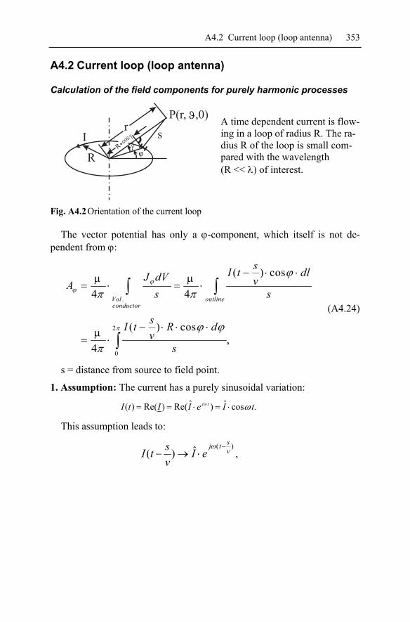
A4.2 Current loop (loop antenna) 353
A4.2 Current loop (loop antenna)
Calculation of the field components for purely harmonic processes
A time dependent current is flow-ing in a loop of radius R. The ra-dius R of the loop is small com-pared with the wavelength (R << λ) of interest.
Fig. A4.2 Orientation of the current loop
The vector potential has only a ϕ-component, which itself is not de-pendent from ϕ:
.
2
0
( ) cos
4 4
( ) cos,
4
Vol outlineconductor
sI t dlJ dV vAs s
sI t R dv
s
ϕϕ
π
ϕ
π π
ϕ ϕ
π
− ⋅ ⋅μ μ= ⋅ = ⋅
− ⋅ ⋅ ⋅μ= ⋅
∫ ∫
∫
(A4.24)
s = distance from source to field point.
1. Assumption: The current has a purely sinusoidal variation:
.cosˆ)ˆRe()Re()( tIeIItI tj ωω ⋅=⋅==
This assumption leads to:
( )ˆ( )sj tvsI t I e
vω −
− → ⋅ ,
354 A4 Elementary Dipoles
( )2
0
sin cos2( )
0
ˆ cosˆ ,4
cos sin cos
ˆ cos .4 sin cos
sj tv
Rjr vj tv
I e RA ds
s r R r R
R I eA e dr R
ωπ
ϕ
ω ϑ ϕπω
ϕ
ϕ ϕπ
γ ϑ ϕ
ϕ ϕπ ϑ ϕ
−
⋅ ⋅−
μ ⋅ ⋅ ⋅= ⋅
= − ⋅ = − ⋅ ⋅ →
μ ⋅ ⋅ ⋅= ⋅ ⋅ ⋅
− ⋅ ⋅
∫
∫
(A4.25)
The exponential expression in the integral is very small (R is small com-pared with λ)
12<<=
λπω RR
v.
Hence, from this condition an approximate solution can be reached via a series expansion of the exponential function:
,1 Ce C +≈ here →⋅⋅+ ϕϑω cossin1vRj
22
( )
0
2 2( )
0 0
( )
2 2 2
cos sin cosˆ
4 sin cos
cos (1 )ˆcos
4 sin cos
ˆ(1 ) 1 .
2 sin sin
rj tv
rj tv
rj tv
RjR I vA e dr R
rjR I ve j d dv r R
I r re jv r R
πω
ϕ
π πω
ω
ϕ ω ϑ ϕϕ
π ϑ ϕ
ϕ ωϖ ϕ ϕ ϕπ ϑ ϕ
ωϑ ϑ
−
−
−
+ ⋅ ⋅μ ⋅ ⋅= ⋅ ⋅
− ⋅ ⋅
⎡ ⎤⋅ +⎢ ⎥μ ⋅ ⋅= ⋅ ⋅ − +⎢ ⎥− ⋅ ⋅⎢ ⎥
⎣ ⎦⎡ ⎤μ ⋅
= ⋅ ⋅ + ⋅ −⎢ ⎥⋅ −⎣ ⎦
∫
∫ ∫ (A4.26)
Using the relation B = rot A , the magnetic field strength can be evalu-ated from the magnetic vector potential.
Fortunately Ar = Aϑ = 0,
2 ( )
2 2 2 3
1 (sin )sinˆ cos (1 ) ,
2 ( sin )
r
rj tv
AH Ar
I R rj evr R
ϑϕ
ω
∂ ∂ϑϑ ∂ϑ ∂ϕ
ϑ ωϑ
−
⎡ ⎤= ⋅ ⋅ −⎢ ⎥μ ⋅ ⋅ ⎣ ⎦
⋅ ⋅= ⋅ + ⋅
⋅ −
(A4.27)

A4.2 Current loop (loop antenna) 355
3( ) 22
2 2 2 2 2 2
32 2 2
2 2 2
2 2 2
4
2 2 2 22 2 2
2 2 2
1 sin ( )sin
ˆ( )
2 sin sin sin
2 sinsin
sin
3 sinsin 1
sin
r
rj tv
AH r Ar r
j rI e r vj r j rr v vr R r R
rr r Rr R
r R
j rvj r r R
v r Rr R
ϑ ϕ
ω
∂ ∂ϑϑ ∂ϕ ∂
ωω ω
ϑ ϑ ϑ
ϑϑ
ϑω
ω ϑϑ
ϑ
−
⎡ ⎤= ⋅ − ⋅ ⋅⎢ ⎥μ ⋅ ⋅ ⎣ ⎦
⎧⎪⋅
= ⋅ ⋅ + − − ⋅⎨⋅ ⋅ − ⋅ − ⋅⎪⎩
⋅ − −− ⋅−
− ⋅
⋅ ⋅ ⋅ − −− ⋅− +
− ⋅
2( )
2 2 2
3 2 2 4 2 2 2
2 2 2 3
2
ˆ( 1 )
2 sin sin
2 32 sin sin 1 2 ,( s in )
rj tv
rjv
r j rI e vj j rv vr R
r r R j r j r Rv v j
r vr r R
ω
ω
ωω ω
ϑ ϑ
ω ωϑ ϑ ωϑ
−
⎫⎪⎪⎪+ ⎬⎪⎪⎪⎭
⎧ +⎪⋅= ⋅ ⋅ − − −⎨⋅ − ⋅⎪
⎩⎫− ⋅ ⋅ ⋅ + − ⋅ ⋅ ⋅ ⎪
− + + ⎬⋅ − ⋅ ⎪
⎭
(A4.28)
0Hϕ = . (A4.29)
2. Assumption: The distance r, of the point P from the annular ring (loop) is much larger than the loop radius: r >> R.
Therefore, an approximate solution is again possible: 3 2
2 2 2 3 222
1 22 2 2 1 22
2
3( sin ) (1 sin ),
21
( sin ) (1 sin )2
Rr R r
rR
r R rr
ϑ ϑ
ϑ ϑ
−−
−−
− ≈ ⋅ + ⋅ ⋅
− ≈ ⋅ + ⋅ ⋅ →
2 ( )ˆ 1( ) cos ( )
4
rj t
vI RH j er r r v
ωωϑ
−= ⋅ ⋅ + ⋅ ⋅ , (A4.30)
( )2 2ˆ 1
( ) sin ( )4
rj t
vI RH j r e
r r v v
ω
ϑ
ω ωϑ
−
= ⋅ ⋅ ⋅ + ⋅ − ⋅⎡ ⎤⎢ ⎥⎣ ⎦
, (A4.31)

356 A4 Elementary Dipoles
.0=ϕH (A4.32)
E is calculated using the 1st Maxwell equation:
1s in1 ( )( )
1 .s in
r
r
r
E r o t HHe
rr H He
r rHe
r
ϑ
ϑϕ
ϑ
ε∂
ϑ ∂ ϕ∂ ∂
∂ ∂ ϑ∂
ϑ ∂ ϕ
•→ →
→
→
→
⋅ =−
= ⋅ ⋅⋅
⋅+ ⋅ ⋅ −
+ ⋅ ⋅⋅
(A4.33)
E has only a ϕ-component:
( )2 3 2
1 ( )( )
ˆ1( ) ( ) sin .4
r
rj tv
r H HEr r
Ij R evr v r
ϑϕ
ω
∂ ∂ε∂ ∂ϑ
ω ω ϑ−
⋅⋅ = ⋅ −
⎡ ⎤= + ⋅ ⋅ ⋅ ⋅ ⋅⎢ ⎥⎣ ⎦
(A4.34)
( )22
ˆs in .
4
rj tvI jE R e
v v r v rω
ϕω ωϑ
ε− ⎡ ⎤= ⋅ ⋅ − ⋅⎢ ⎥⎣ ⎦
(A4.35)
0rE Eϑ= = , (A4.36)
Through use of the wavelength,
ελπω
λπω
ωπλ
⋅μ⋅==→==
2;22v
vfv ,
a very illustrative solution can be found:
.sin2)2(1)(4
ˆ
;0
)(22 ϑλπ
λπ
ε
ωϕ
ϑ
⋅⋅⎥⎦⎤
⎢⎣⎡ −⋅⋅
μ⋅⋅=
==
−vrtj
r
erjrrr
RIE
EE
(A4.37)

A4.2 Current loop (loop antenna) 357
The real parts lead to the time dependent solution:
2
2
1ˆ( ) ( ) cos2
2cos( ( )) sin ( ( ))
ˆ ( ) cos
cos( ( )) sin ( ( )) ,2
rRH t Ir r
r r rt tv v
RIr
r rt tr v v
ϑ
πω ωλ
π ϑλ
λ ω ωπ
= ⋅ ⋅ ⋅
⎧ ⎫⋅ − − ⋅ −⎨ ⎬⎩ ⎭
= ⋅ ⋅ ⋅
⎧ ⎫⋅ ⋅ − − −⎨ ⎬⎩ ⎭
(A4.38)
2
2
32
3
3 2
1ˆ( ) ( ) sin42 2[1 ( ) ] cos( ( )) sin( ( ))
2ˆ sin
[( ) ] cos( ( )) ( ) sin( ( ))2 2 2
RH t Ir r
r r r rt tv v
I R
r rt tr r v r v
ϑ ϑ
π πω ωλ λ
π ϑλλ λ λω ωπ π π
= ⋅ ⋅ ⋅
⎧ ⎫⋅ − ⋅ − − ⋅ −⎨ ⎬⎩ ⎭
= ⋅ ⋅ ⋅
⎧ ⎫⋅ − ⋅ − − ⋅ −⎨ ⎬⎩ ⎭
(A4.39)
( ) 0H tϕ = , (A4.40)
( ) ( ) 0rE t E tϑ= = . (A4.41)
2
32
3
2
ˆ 1( ) ( ) sin4
2 2( ) cos( ( )) sin( ( ))
2ˆ sin
cos( ( )) ( ) sin( ( )) .2 2
I RE tr r
r r r rt tv v
I R
r rt tr v r v
ϕ ϑε
π πω ωλ λ
π ϑε λλ λω ωπ π
μ= ⋅ ⋅ ⋅ ⋅
⎧ ⎫⋅ ⋅ − + ⋅ −⎨ ⎬⎩ ⎭
μ= ⋅ ⋅ ⋅ ⋅
⎧ ⎫⋅ ⋅ − + ⋅ −⎨ ⎬⎩ ⎭
(A4.42)

358 A4 Elementary Dipoles
Far field (r > λ/2π)
Only terms with the highest power of r are now significant. It becomes clear that ϑHH r << .
0)( =tHr , (A4.43)
ϑωλ
πϑ sin))(cos(ˆ)()( 2
2
⋅−⋅⋅⋅−=vrtIR
rtH , (A4.44)
.sin))(cos(ˆ)()( 22
ϑωελ
πϕ ⋅−⋅
μ⋅⋅⋅=
vrtIR
rtE (A4.45)
It can be seen that E and H are in phase. The ratio of the two, as with the Hertzian dipole, is constant and equal to
.εϑ
ϕ μ=−=Γ
HE
Radiated power and radiation resistance (far field)
Poynting-vector
4 4 22
2 2
0 5
1 ˆ( ) ( )
cos ( ( )) sin ,
r
time mean value ,
S E H R Ir
rt
ϕ ϑμ πε λ
ω ϑν
=
= ⋅ − = ⋅ ⋅ ⋅ ⋅
⋅ − ⋅ (A4.46)
4 2 2
0 ,
ˆ1( ) ( ) s in .
2r m it te l
S S
R IS
r
ϑ ϕ
πϑ
ε λ
= =
μ= ⋅ ⋅ ⋅ ⋅
(A4.47)
Average radiated power Pa:

A4.2 Current loop (loop antenna) 359
.ˆ)(3
4
sinˆ)(
sin2
24
3/40
324
2
0
εμ
λππ
ϑϑπλπ
εμ
ϑϑπ
π
π
⋅⋅⋅=
⋅⋅⋅=
⋅⋅⋅=⋅=
∫
∫∫
IR
dIR
drSdASP mittelrra
surfaceSphere
mittel
(A4.48)
Radiation resistance:
.)(3
8)2/ˆ(
4
2 ελππ μ
⋅⋅==R
IPR a
a (A4.49)
For µ = µ0 and ε = ε0 (vacuum), the wave impedance becomes
Ωε
Γ 3770
00 =
μ= , (A4.50)
and the radiation resistance
Ω⎟⎠
⎞⎜⎝
⎛⋅⋅=4
40 107.30
λR
Ra . (A4.51)
Near field (r < λ/2π)
Only terms with the lowest power of r are considered. The wave retarda-tion is neglected.
2 1ˆ( ) ( ) c o s c o s ,2r
RH t I t
r rϑ ω= ⋅ ⋅ ⋅ (A4.52)
2 1ˆ( ) ( ) s in c o s ,4
RH t I tr rϑ ϑ ω= ⋅ ⋅ ⋅ ⋅ (A4.53)
2ˆ
( ) ( ) s in s in .2I R
E t trϕ
πϑ ω
ε λμ
= ⋅ ⋅ ⋅ ⋅ ⋅ (A4.54)
Wave impedance:

360 A4 Elementary Dipoles
ελπ
ϑ
ϕ μ⋅+=−=Γ
rjH
EW
2 . (A4.55)
This wave impedance wΓ is inductive, and its magnitude is smaller
then that of the far field wave impedanceμ
Γ =ε
. This is because, in the
near field, λ/2πr < 1. Therefore, the field is called a low-impedance field.
A4.3 Comparison of the wave impedances
Hertzian di-pole
Near field 2W j
rλπ ε
μΓ = − ⋅ ⋅ High impedance
field
Far field W εμ
Γ ≡ Γ =
Current loop Near field
2W
rj
πλ ε
μΓ = + ⋅ ⋅ Low impedance
field
Far field W εμ
Γ ≡ Γ =
A diagram of the wave impedances as functions of the distance from the source is given in chapter 5.2.2.

A5 The Polarization Ellipsis
In dealing with electromagnetic fields the question often arises as to how to add together several components of a certain vector quantity, which can each have different phases (for instance Ex, Ey, Ez). Regarding the subject of EMC, with relation to the field strength value, one generally refers to the substituting field strength. This quantity results from the addition of the squared field quantities with a subsequent square route operation:
222zyxges EEEE ++= . (A5.1)
The following points will be dealt with in this annex chapter: • It will be shown that the head of the vector of a field quantity, con-
sisting of several components, moves in a plane elliptical orbit. • The absolute maximum value will be predicted with consideration
of the phases. • The conditions will be derived that form a circular orbit (circular po-
larization), which is a special case of an elliptical orbit (elliptical po-larization).
In doing so, the solutions for the two and the three dimensional cases are presented. For the three dimensional case, two solution procedures are stated:
1. The solution procedure in the time domain, 2. The solution procedure in the frequency domain; more precisely, via
complex or symbolic calculus.
It must be admitted that the solution procedure via the time domain is simple, but very costly. This method of obtaining the solution has the ad-vantage that it is easily understood. The solution procedure using complex calculus is much shorter. On one hand, it demonstrates the advantages of performing calculus in the frequency domain. On the other hand, it is very difficult to understand if no knowledge of complex calculus exists. For fur-ther details the reader is directed to the paper [AD/ME73].
K.-H. Gonschorek, R. Vick, Electromagnetic Compatibility for Device Design and System Integration, DOI 10.1007/978-3-642-03290-5_16, © Springer-Verlag Berlin Heidelberg 2009
362 A5 The Polarization Ellipsis
The relations ( )2/sincos π+= xx and ( )2/cossin π+−= xx are regu-larly used in the following derivations. The procedure starts by assuming that the vector consists of the following three components:
( )( )( ) .sincoscos
,sincoscos,sincoscos
zzzzz
yyyyy
xxxxx
jZZEtZEjYYEtYEjXXEtXE
ϕϕϕω
ϕϕϕωϕϕϕω
⋅+⋅=→+=
⋅+⋅=→+=
⋅+⋅=→+=
(A5.2)
The polarization ellipse is formed as the path of the locus of field vector in space, which is the result of the addition of the squared field values (considering the time dependence) with a subsequent square route opera-tion.
A5.1 Two dimensional case (Ez=0)
Only the time domain solution is shown for the two dimensional case. Both the time domain and the frequency domain solution are included for the three dimensional case. The two dimensional case has special impor-tance within EMC-measurement techniques. Therefore, the well-known time domain solution is reproduced here.
The length of the resulting vector, including its algebraic sign, is ob-tained from the addition of Ex and Ey and is given by
( ) ( )( )( )
( )( )( )
( )
( )( )
2 2 2 2
2
2
2 2 2
2
2 2
4 4 2 2
cos cos
1 cos 2 212 1 cos 2 2
cos 2 212 cos 2 2
12 cos 2 2 ,
2sin 2
x y
x
y
x
y
y x
k
K X t Y t
X t
Y t
X Y X t
Y t
X Y
X Y X Y
t
ω ϕ ω ϕ
ω ϕ
ω ϕ
ω ϕ
ω ϕ
ϕ ϕ
ω ϕ
= ± ⋅ + + ⋅ +
+ += ± ⋅
+ + +
+ + ⋅ += ± ⋅
+ ⋅ +
+
= ± ⋅ + + + ⋅ −
⋅ +
(A5.3)
A5.1 Two dimensional case (Ez=0) 363
.2sin2sin2cos2cos
arctan 22
22
yx
yxk YX
YXϕϕϕϕ
ϕ⋅−⋅−
⋅+⋅= (A5.4)
Drawing a curve showing the location of K as function of ωt, in a polar coordination system, yields an ellipse.
1. The maximum of the polarization ellipse is calculated from the rela-tion
( ) 12sin =+ kt ϕω ,
resulting in
ππϕπππϕω
42
2,2
22 Tntnt kk ⎟
⎠⎞
⎜⎝⎛ ⋅+−=⋅+=+ (A5.5)
Examples:
a) 22,2
,20
0YXKTntk
y
x +=⋅==⎭⎬⎫
== πϕ
ϕϕ
The ellipsis becomes a straight line.
b) 22
22
for2
for2
2
0
YX
YXk
y
x
<−
>=
⎪⎭
⎪⎬⎫
=
=
π
π
ϕπϕ
ϕ
( )
2 2 4 4 2 2
2 2 4 4 2 2
1, für
2 21
2 1 , für4 2
nt T K X Y X Y X Y
Tt n K X Y Y X X Y
⇒ = = + + − >
= + = + − − <
2. The minimum of the ellipse is calculated from
( )sin 2 1, and results in
3 32 2 , 2 .
2 2 4
k
k k
t
Tt n t n
ω ϕ
π πω ϕ π ϕ π
π
+ = −
+ = + ⋅ = − + ⋅⎛ ⎞⎜ ⎟⎝ ⎠
(A5.6)
3. In order to produce circular polarization, the amplitude of the total oscillation must be independent of time.
( ) 022cos2 2244 =−⋅++⇒ xyYXYX ϕϕ This condition can only be fulfilled for
( ) 2 2cos 2 2 1 and X .y x Yϕ ϕ− = − =

364 A5 The Polarization Ellipsis
Verbally: Circular polarization is only obtained in the two dimen-sional case if the amplitude of the two components are equal, if the components are located orthogonal to each other and if the time phase difference between the two components amounts to 090± .
( ).12
2
,
+±=−
=
n
YX
xy
πϕϕ
4. Through a time shifting of ωt = -ϕx it is possible to reach ϕx = 0 and ϕy’ = ϕy - ϕx . Polarization ellipses are shown in Fig. A5.1 for vari-ous amplitude values and phase angles.
1. X = 4 Y = 4 ϕx = 0 ϕy = 90
2. X = 4 Y = 2 ϕx = 0 ϕy = 90 3. X = 4 Y = 4 ϕx = 0 ϕy = 45
y
x
2
3
1
4
t = 0t = 0
t = 0t = 0
t = T/8t = T/8
4. X = 4 Y = 2 ϕx = 0 ϕy = 45
Fig. A5.1 Polarization ellipses for the two dimensional case
A5.2 Three dimensional case – solution in the time domain
With ( ),2sin kp tPE ϕω +⋅=
( )xyYXYXP ϕϕ 22cos2 2244 −⋅++= , (A5.7)

A5.2 Three dimensional case – solution in the time domain 365
and ( ),cos zz tZE ϕω +⋅=
( )( ),22cos12122
zz tZE ϕω ++= (A5.8)
one obtains
( )
( )
( )( )
2 2 2
2
2 4 2
2 2 2
2 4 22 2 2
2
2
sin 21 ,2 sin 2 2
2
21 sin 2 ,2 cos 2
2
21 sin 2 ,2 sin 2
sin cosarctan ,cos sin
k
z
sz k
sz k
k zs
k z
X Y Z P tS
Z t
P Z P ZS X Y Z t
P Z P ZS X Y Z t
P ZP Z
ω ϕ
πω ϕ
ω ϕπϕ ϕ
ω ϕϕ ϕ
ϕ ϕϕϕ ϕ
+ + + ⋅ += ⋅ ⎛ ⎞+ ⋅ + +⎜ ⎟
⎝ ⎠
+ + ⋅= ⋅ + + + ⋅ +⎛ ⎞⋅ + −⎜ ⎟
⎝ ⎠
+ − ⋅= ⋅ + + + ⋅ +
⋅ −
⋅ + ⋅=
⋅ − ⋅
(A5.9)
⎟⎠⎞⎜
⎝⎛ +⋅
⎟⎠⎞⎜
⎝⎛ −⋅⋅
⎟⎠⎞
⎜⎝⎛ −⋅
++−
⎟⎠⎞
⎜⎝⎛ −⋅
+++
+++=
st
kzZ
xy
YXYX
xy
YXZYX
ZYXS
ϕω
ϕϕ
ϕϕ
ϕϕ
2sin
2sin2
22cos
22244
2
22cos
222444
222
21
. (A5.10)
Drawing the location curve S in a Cartesian-coordinate system, by en-tering the individual components for different phases ωt and adding them, yields an ellipse.
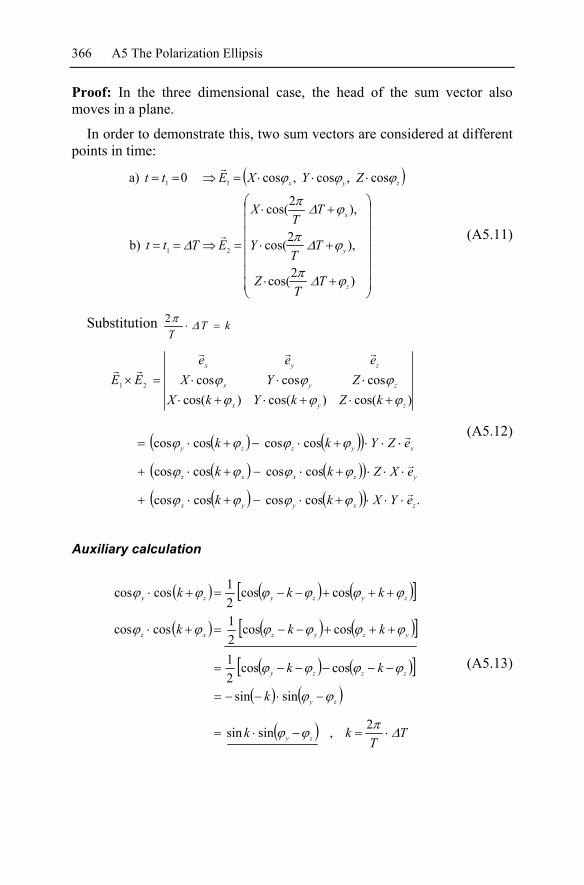
366 A5 The Polarization Ellipsis
Proof: In the three dimensional case, the head of the sum vector also moves in a plane.
In order to demonstrate this, two sum vectors are considered at different points in time:
( )
⎟⎟⎟⎟⎟⎟⎟
⎠
⎞
⎜⎜⎜⎜⎜⎜⎜
⎝
⎛
+⋅
+⋅
+⋅
=⇒==
⋅⋅⋅=⇒==
)2cos(
),2cos(
),2cos(
b)
cos,cos,cos0 a)
21
11
z
y
x
zyx
TT
Z
TT
Y
TT
X
ETtt
ZYXEtt
ϕΔπ
ϕΔπ
ϕΔπ
Δ
ϕϕϕ
(A5.11)
Substitution kTT
=⋅ Δπ2
( ) ( )( )( ) ( )( )( ) ( )( ) .coscoscoscos
coscoscoscos
coscoscoscos
)cos()cos()cos(coscoscos21
zxyyx
yzxxz
xyzzy
zyx
zyx
zyx
eYXkk
eXZkk
eZYkk
kZkYkXZYX
eeeEE
⋅⋅⋅+⋅−+⋅+
⋅⋅⋅+⋅−+⋅+
⋅⋅⋅+⋅−+⋅=
+⋅+⋅+⋅⋅⋅⋅=×
ϕϕϕϕ
ϕϕϕϕ
ϕϕϕϕ
ϕϕϕϕϕϕ
(A5.12)
Auxiliary calculation
( ) ( ) ( )[ ]
( ) ( ) ( )[ ]
( ) ( )[ ]( ) ( )
( ) TT
kk
k
kk
kkk
kkk
zy
zy
zzzy
yzyzxz
zyzyzy
Δπϕϕ
ϕϕ
ϕϕϕϕ
ϕϕϕϕϕϕ
ϕϕϕϕϕϕ
⋅=−⋅=
−⋅−−=
−−−−−=
+++−−=+⋅
+++−−=+⋅
2,sinsin
sinsin
coscos21
coscos21coscos
coscos21coscos
(A5.13)

A5.2 Three dimensional case – solution in the time domain 367
( ) ( ) ( )( ) ( ) ( )yxxyyx
xzzxxz
kkk
kkk
ϕϕϕϕϕϕ
ϕϕϕϕϕϕ
−⋅=+⋅−+⋅
−⋅=+⋅−+⋅
sinsincoscoscoscos
sinsincoscoscoscos
( )( )( )
( )
( )( )( )
( )( )( )yx
xz
zy
yx
xz
zy
yx
xz
zy
YXXZ
ZY
XYZXYZ
EEe
TT
XYZXYZ
EE
ϕϕ
ϕϕ
ϕϕ
ϕϕϕϕ
ϕϕ
Δπ
ϕϕϕϕ
ϕϕ
−⋅+
−⋅+
−⋅
⎟⎟⎟⎟
⎠
⎞
⎜⎜⎜⎜
⎝
⎛
−⋅
−⋅
−⋅
=×
⋅⋅⎟⎟⎟⎟
⎠
⎞
⎜⎜⎜⎜
⎝
⎛
−⋅
−⋅
−⋅
=×⇒
222
222
22221
21
sinsin
sin
sin,sin,sin
2sinsin
,sin,sin
(A5.14)
It can be seen from this solution that the unit vector is independent of time 2t and therefore all sum vectors must lie in a common plane. The di-rection of the plane’s normal vector can be easily predicted using this pro-cedure.
A5.2.1 Some consideration regarding the plane of the polarization ellipse
(1) Creation of a coordinate system x’’,y’,z’ containing the polarization ellipse in its y’,z’-plane
A coordinate system is produced in which the plane vector of the polariza-tion ellipse points in the x’-direction by:
a) Turning the x-axis of the xy-plane into the x’-axis, in such a way that the y’- axis lies in the plane of the polarization ellipse.
( )( )zy
xz
YZZX
yxy
yxx
ϕϕϕϕ
ϕ
ϕϕ
ϕϕ
−⋅−⋅
=
⋅+⋅−=
⋅+⋅=
sinsin
arctan
cossin'
sincos'
1
11
11
(A5.15)

368 A5 The Polarization Ellipsis
b) Rotating the z-axis around the y’-axis by an angle of 2ϕ , , in such a way that the x’-axis becomes the x’’-axis and coincides with the unit vector of the polarization plane (now the z’-axis also lies in the plane of the polarization ellipse).
( )( ) ( )xzzy
yx
XYZ
YXzxz
zxx
ϕϕϕϕ
ϕϕϕϑ
ϕϕϕϕ
−⋅+−⋅
−⋅⋅−=−=
⋅+⋅−=⋅+⋅=
22220
20
22
22
sinsin
sinarctan9090
cossin''sincos'''
(A5.16)
(2) Angle of the plane normal vector with the x-,y-,z- axes
The angles between the plane normal vectors of the polarization ellipse to the x, y and z-axis can now be predicted using the scalar product.
axes theof vector
vectornormal plane
cos,cos
=
=
⋅⋅
=⋅⋅=⋅
b
ababababa ϑϑ
(A5.17)
( ) ( )( )( ) ( )( )( ) ( )( )yxzyxz
xzyxzy
zyxzxx
XYXY
ZXZX
YZYZ
ϕϕϑϕϕϑ
ϕϕϑϕϕϑ
ϕϕϑϕϕϑ
−⋅=−⋅=
−⋅=−⋅=
−⋅=−⋅=⇒
sinarccos,sincos
sinarccos,sincos
sinarccos,sincos
(A5.18)
(3) The maximum value (minimum value) of the sum vector
The semimajor and semiminor axis of the polarization ellipse determine the maximum and the minimum value of the ellipse respectively.
The maximum of the polarization ellipse is given for ( ) 12sin =+ st ϕω .
ππϕπππϕω
42
2,2
22 Tntnt ks ⋅⎟
⎠⎞
⎜⎝⎛ ⋅+−=⋅+=+⇒ (A5.19)
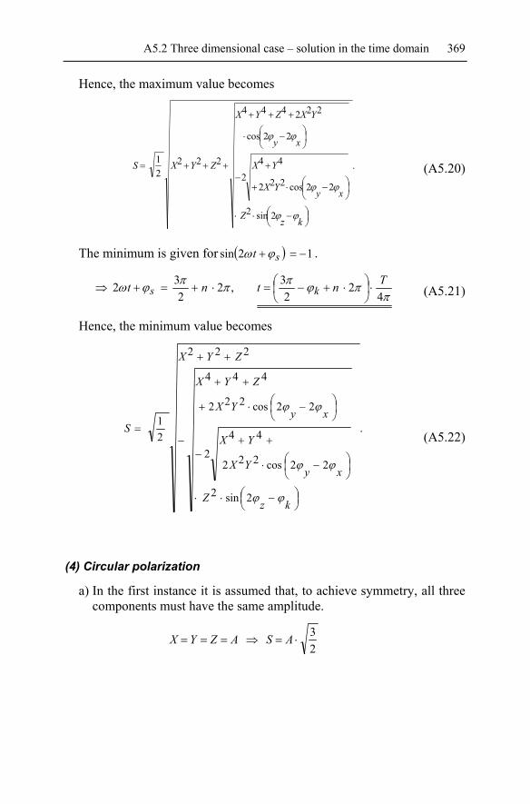
A5.2 Three dimensional case – solution in the time domain 369
Hence, the maximum value becomes
.
2sin2
22cos222
44
2
22cos
222444
22221
⎟⎠⎞⎜
⎝⎛ −⋅⋅
⎟⎠⎞
⎜⎝⎛ −⋅+
+−
⎟⎠⎞
⎜⎝⎛ −⋅
+++
+++=
kzZ
xyYX
YX
xy
YXZYX
ZYXS
ϕϕ
ϕϕ
ϕϕ
(A5.20)
The minimum is given for ( ) 12sin −=+ st ϕω .
ππϕπππϕω
42
23,2
232 Tntnt ks ⋅⎟
⎠⎞
⎜⎝⎛ ⋅+−=⋅+=+⇒ (A5.21)
Hence, the minimum value becomes
.
2sin2
22cos222
44
2
22cos222
444
222
21
⎟⎠⎞⎜
⎝⎛ −⋅⋅
⎟⎠⎞
⎜⎝⎛ −⋅
++−
⎟⎠⎞
⎜⎝⎛ −⋅+
++
−
++
=
kzZ
xyYX
YX
xyYX
ZYX
ZYX
S
ϕϕ
ϕϕ
ϕϕ
(A5.22)
(4) Circular polarization
a) In the first instance it is assumed that, to achieve symmetry, all three components must have the same amplitude.
23
⋅=⇒=== ASAZYX
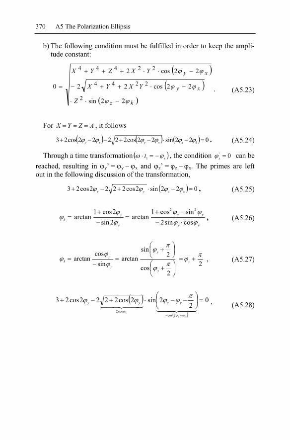
370 A5 The Polarization Ellipsis
b) The following condition must be fulfilled in order to keep the ampli-tude constant:
( )( )
( )kz
xy
xy
Z
YXYX
YXZYX
ϕϕ
ϕϕ
ϕϕ
22sin
22cos22
22cos2
0
2
2244
22444
−⋅⋅
−⋅++−
−⋅⋅+++
= . (A5.23)
For AZYX === , it follows
( ) ( ) ( ) 022sin22cos22222cos23 =−⋅−+−−+ kzxyxy ϕϕϕϕϕϕ . (A5.24)
Through a time transformation ( )xt ϕω −=⋅ 1 , the condition 0' =xϕ can be reached, resulting in ϕy’ = ϕy – ϕx and ϕz’ = ϕz – ϕx. The primes are left out in the following discussion of the transformation,
( ) 022sin2cos2222cos23 =−⋅+−+ kzyy ϕϕϕϕ , (A5.25)
yy
yy
y
yk ϕϕ
ϕϕϕϕ
ϕcossin2sincos1
arctan2sin2cos1
arctan22
⋅−−+
=−+
= , (A5.26)
22
cos
2sin
arctansin
cosarctan πϕ
πϕ
πϕ
ϕϕ
ϕ +=⎟⎠⎞
⎜⎝⎛ +
⎟⎠⎞
⎜⎝⎛ +
=−
= y
y
y
y
yk , (A5.27)
( )( )
02
2sin2cos2222cos23
2coscos2
=⎟⎠⎞
⎜⎝⎛ −−⋅+−+
−− yz
yz
y
yy
ϕϕϕ
πϕϕϕϕ , (A5.28)

A5.2 Three dimensional case – solution in the time domain 371
( )
( )
( )
( )
( ) ( )( ).12cos41
22cos
cos
,41cos2coscos
12coscos4cos4
,12coscos42cos22
,32coscos42cos2
2
2
2 ,
−−±−
−=
−=⋅−+
−=−⋅+⋅
−=−⋅++
−=−⋅+
yzyz
y
yyzy
yzyy
yzyy
yzyy
ϕϕϕϕ
ϕ
ϕϕϕϕ
ϕϕϕϕ
ϕϕϕϕ
ϕϕϕϕ
(A5.29)
A real solution is only given for the condition
( )
.22
2
3 2, 1, 0, ,2
12cos2
yz
yz
yz
yz
n
n
nn
ϕπϕ
ϕπϕ
πϕϕ
ϕϕ
+⋅=
+⋅=
=⋅=−
=−
(A5.30)
( )
00
00
00
00
240,120
300,60:1
120,60
240,120:02
coscos
=
==
=
==⇒
⋅−=⇒
z
y
z
y
y
n
n
n
ϕ
ϕ
ϕ
ϕ
πϕ
(5) Circular polarization for the general case
( )( )
( )kz
xy
xy
Z
YXYX
YXZYX
ϕϕ
ϕϕ
ϕϕ
22sin
22cos22
22cos2
02
2244
22444
−⋅⋅
−++−
−+++
= (A5.31)
⇒= 0xϕ

372 A5 The Polarization Ellipsis
( )( ) ( )kzy
y
ZYXYX
ZYXZYX
ϕϕϕ
ϕ
22sin2cos22
2cos2022244
422444
−⋅⋅++−
++++=
Simplification:
( )( )( ) ( )
4 4 2 2
2 2 4
2 4 2 41,2
2 cos2
2 sin 2
sin 2 sin 2
y
z k
z k z k
V X Y X Y
V V Z Z
V Z Z Z
ϕ
ϕ ϕ
ϕ ϕ ϕ ϕ
= + +
⇒ − ⋅ − = −
= ⋅ − ± ⋅ − −
(A5.32)
A real solution is only given for the condition
( ) ( )122
2,12sin2 +=−=− nkzkz
πϕϕϕϕ ,
22,1 ZV ±= ,
( )
( ) 42244
22244
2cos2
2cos2
ZYXYX
ZYXYX
y
y
=++
±=++
ϕ
ϕ, (A5.33)
( )
.2
arccos21
,2
2cos
22
444
22
444
YX
YXZ
YX
YXZ
y
y
−−⋅=
−−=
ϕ
ϕ
(A5.34)
Applying the values X = Y = Z results in the already known solution.
Given the condition that yϕ2cos is not allowed to become larger than 1, and not smaller than –1, the following stipulations can be derived:
I.)
( ) ( ) 4222222422
444
,012
ZYXYXZYX
YXZ≥+≤+−⇒≤
−− , (A5.35)
II.)
( ) 422222
444
12
ZYXYX
YXZ≤−⇒−≥
−− . (A5.36)

A5.2 Three dimensional case – solution in the time domain 373
From the 2 previous equations it follows
( ) ( )2224222 YXZYX +≤≤− (A5.37)
III.) It is also possible to derive conditions for 44 and YX . However, for reasons of symmetry, they must have a similar shape.
The amplitude (radius) of the total oscillation (of the circle) amounts to
222
21 ZYXS ++= (A5.38)
Example A5.1: For Z4 = X4 + Y4, the necessary phase angle ϕy (ϕx = 0 has been assumed for the derivation of these relations) is calculated from
°== 4502cos yy beto ϕϕ .
In order to predict the value of ϕz, the phase angle ϕk, according to Eq. (A5.4), must be known. It is calculated from
2
k 2
X=arctan
-Yϕ .
Choosing X2 = Y2 , for instance, yields a value of ϕk = 1350.
Having predicted ϕk it is possible to determine ϕz. According to Eq. (A5.30) the result is
0kz
π j= + = 112.5 for n = 1.
4 2ϕ
The amplitudes X = 0.841, Y = 0.841, and Z = 1 satisfy the assumptions above. The amplitude (radius) of the total oscillation (of the circle) can be calculated using these values to be equal to
.099.11707.0707.021
=++⋅=S
The polarization circle for the values mentioned previously is presented in Fig. A5.2.

374 A5 The Polarization Ellipsis
z
y
x
t = 0
t = 0
t = T/8
t = 3T/16
t = 3T/8
t = T/2
10 e
t = 5T/8
t = 3T/4
t = T/16 t = /8
S
Fig. A5.2 Polarization circle for X = 0.841, Y = 0.841, Z = 1, ϕx = 0°, ϕy = 45°,
ϕz = 112.5°
The plane containing the polarization circle has a normal vector given by
( ) ( )414.0,644.0,644.021 −−=× EEeS .
Please also see Eq. (A5.14).
Given the angles according to Eqs. (A5.15), (A5.16) and (A5.18), the following values can be determined,
00
01 135
)5.67sin(841.0
5.112sin841.0arctan =−⋅
⋅=ϕ ,
( )
0
022022
022
5.24
)5.112(sin841.0)5.67(sin841.0
45sin841.0arctan
−=
⋅+−⋅
−⋅=ϕ
,
( ) 00 141)5.67sin(841.0arccos =−⋅=xϑ ,
( ) 00 39)5.112sin(841.0arccos =+⋅=yϑ ,
( ) 002 120)45sin(841.0arccos =−⋅=zϑ .
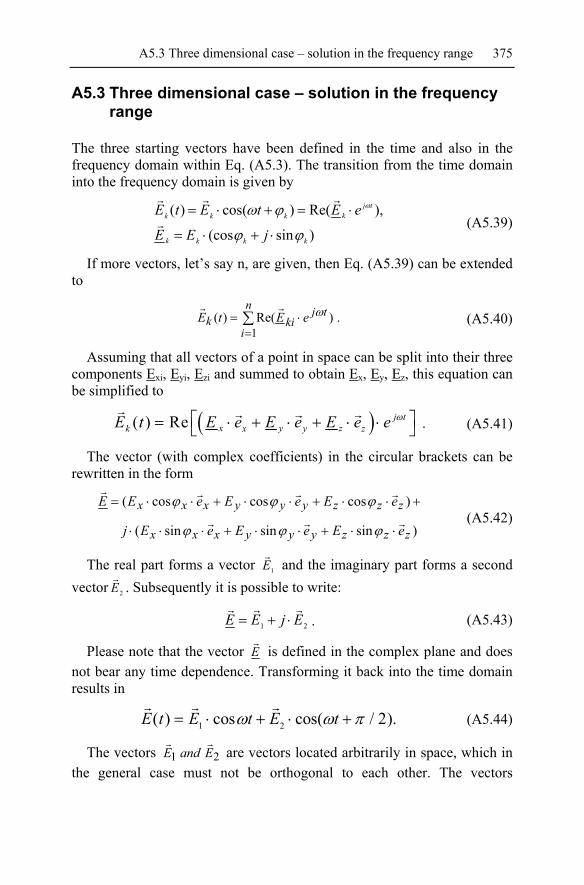
A5.3 Three dimensional case – solution in the frequency range 375
A5.3 Three dimensional case – solution in the frequency range
The three starting vectors have been defined in the time and also in the frequency domain within Eq. (A5.3). The transition from the time domain into the frequency domain is given by
)sin(cos
),Re()cos()(
kkkk
tjkkkk
jEE
eEtEtE
ϕϕ
ϕω ω
⋅+⋅=
⋅=+⋅= (A5.39)
If more vectors, let’s say n, are given, then Eq. (A5.39) can be extended to
.)Re()(1
∑=
⋅=n
i
tjkik eEtE ω (A5.40)
Assuming that all vectors of a point in space can be split into their three components Exi, Eyi, Ezi and summed to obtain Ex, Ey, Ez, this equation can be simplified to
( )( ) Re j tx y zk x y zE t E e E e E e e ω⎡ ⎤= ⋅ + ⋅ + ⋅ ⋅⎣ ⎦ . (A5.41)
The vector (with complex coefficients) in the circular brackets can be rewritten in the form
)sinsinsin(
)coscoscos(
zzzyyyxxx
zzzyyyxxx
eEeEeEj
eEeEeEE
⋅⋅+⋅⋅+⋅⋅⋅
+⋅⋅+⋅⋅+⋅⋅=
ϕϕϕ
ϕϕϕ (A5.42)
The real part forms a vector 1E and the imaginary part forms a second vector 2E . Subsequently it is possible to write:
21 EjEE ⋅+= . (A5.43)
Please note that the vector E is defined in the complex plane and does not bear any time dependence. Transforming it back into the time domain results in
1 2( ) cos cos( / 2).E t E t E tω ω π= ⋅ + ⋅ + (A5.44)
The vectors 21 EandE are vectors located arbitrarily in space, which in the general case must not be orthogonal to each other. The vectors

376 A5 The Polarization Ellipsis
21 EandE −− exist spatially in the opposite direction with relation to
21 EandE . )()( 21 tEandtE oscillate with ωt dependence and a mutual phase shift of π/2, resulting in )(tE moving from 1E to 2E at ωt = π/2, to
1E− at ωt = π, to 2E− at ωt = 3π/2 and back to 1E at ωt = 2π. The head of the resulting vector lies in a common plane.
The angle ϑ between the two vectors can be easily predicted via the vector expression
1 2
1 2
arccos .E EE E
ϑ⋅
=⋅
(A5.45)
Defining now a new coordinate system ),( yx ee , in which the vector 1E
coincides with the x-axis, it is possible to split the vector 2E into two parts in such a way that an orthogonal pair is obtained, which coincide with the axes of this new coordinate system.
yx eEeEE ⋅⋅+⋅⋅= ϑϑ sincos 222 (A5.46)
In this new coordinate system the following two vectors are given
.)2/cos(sin)(
,))2/cos(coscos()(
2
21
yy
xx
etEtE
etEtEtE
⋅+⋅⋅=
⋅+⋅⋅+⋅=
πωϑ
πωϑω (A5.47)
Eq. (A5.47) describes the two dimensional case, which has already been treated in chapter A5.1.
Please also refer to the publication [FAR03], in which additional secon-dary literature about the polarization ellipse is given.

A6 Skin Effect and Shielding Theory of Schelkunoff
A basic knowledge and understanding of the theory of the skin effect and eddy currents are necessary so that efficient measures are taken to achieve the EMC of an arrangement. The current in a conductor flows more and more on the surface of a conductor with increasing frequency due to the so-called skin effect. More accurately, it flows in a thinner and thinner layer on the surface of the conductor. The skin effect is often referred to as the effect of current displacement (to the exterior). In annex chapter A6.1, the theory is applied to the conducting half space and it is shown that cy-lindrical conductors can also be treated in a very simple way.
Theory regarding the shielding of electromagnetic fields using an im-pedance concept was first written down by Schelkunoff and is therefore called Schelkunoff’s theory. This theory should be understood from its fundamental consequences. Therefore, in chapter A6.2, Schelkunoff’s the-ory is repeated from its basic principles.
A6.1 Skin effect of a conducting half space
Fig. A6.1 Conducting half space, in which a current I is flowing
K.-H. Gonschorek, R. Vick, Electromagnetic Compatibility for Device Design and System Integration, DOI 10.1007/978-3-642-03290-5_17, © Springer-Verlag Berlin Heidelberg 2009

378 A6 Skin Effect and Shielding Theory of Schelkunoff
A sinusoidal current, I(t) = Re(I(t)) = Re(I ejωt), is assumed in the fol-lowing considerations. Furthermore, only the one-dimensional case is trea-ted.
Current den-
sity xxxx eEeJJ ⋅⋅=⋅= κ (A6.1)
Magnetic fiel-d yy eHH ⋅= (A6.2)
dtDdJHrot += Ampere’s law (A6.3)
Maxwells equations
dtHdErot ⋅−μ= Faraday’s law (A6.4)
Using the aforementioned conditions and neglecting the expression
dtDd yields
⎪⎪⎭
⎪⎪⎬
⎫
⋅−μ=
⋅−=
tH
zE
Ez
H
yx
xy
∂∂
∂∂
κ∂∂
0
22
2
2
2
=⋅μ−
⋅μ=
yy
yy
HjzH
HjzH
γκω
∂∂
κω∂∂
. (A6.5)
For the one-dimensional case the following solutions are obtained:
zyy eHH ⋅−⋅= γ
0 (A6.6a)
zzyx eEeHE ⋅−⋅− ⋅=⋅⋅= γγ
κγ
00 (A6.6b)
zzyx eJeHJ ⋅−⋅− ⋅=⋅⋅= γγγ 00 (A6.6c)
djjj 1)1( ⋅+=⋅+=μ= βακωγ (A6.7)
2d
ω κ=
μ skin depth or thickness of the
equivalent conducting layer (A6.8)
A6.1 Skin effect of a conducting half space 379
Within a strip of a width Δy, a current given by
∫⋅
=⋅⋅
−=⋅⋅=∞ ∞
⋅−⋅−
0
0
0
00 /
γΔ
γΔΔ γγ
Δ
JyeJydzeJyI zzy (A6.9)
flows. The voltage drop across a 1 m length of the surface becomes
mJdxEUm
100
1
0⋅=∫=
κ. (A6.10)
Dividing the voltage drop by the current flowing gives the impedance of the strip Δy:
κγ
ΔΔγ
κΔ ⋅=⋅
⋅⋅==y
mJy
mJIUZ y
110
0 , (A6.11)
iy LjRjdymZ ω
κΔΔ +=+⋅⋅
=⇒ ~)1(1 . (A6.12)
Expressing this impedance in terms of a 1 metre length yields:
''~
' )1(iy LjR
dyjZ ωκΔΔ +=⋅⋅
+= . (A6.13)
It is interesting to note with this result, that the real and the imaginary parts are equal. If we consider only the real part, we get the DC-resistance per metre of a strip conductor with thickness d (skin depth = thickness of the equivalent conducting layer) and width Δy.
In the case of a cylindrical conductor a very simple solution is also pos-sible, if only two extreme cases are considered.
A6.1.1 Strong skin effect within a cylindrical conductor
Strong skin effect is defined as the case where the radius of the cylindrical conductor is essentially larger than the skin depth ( dR >> ). This assumption results in
( ) ( )jd
RRjdR
Z +⋅=+⋅⋅
= = 12
'12
1'0 κπ, (A6.14)
380 A6 Skin Effect and Shielding Theory of Schelkunoff
with
κπ ⋅== 2
1'R
R . (A6.15)
A6.1.2 Weak skin effect within a cylindrical conductor
Weak skin effect is defined as the case where the radius of the cylindrical conductor is essentially smaller than the skin depth ( dR << ).
This assumption results in:
↑⋅
=κπ 20
1'R
Z ↑
+πμω
8j (A6.16)
DC-resistance per metre
Inductive reactance per me-tre (derivation is trivial)
It is interesting to note that, with the result for the weak skin effect, the inner inductive reactance per metre of a cylindrical conductor is not a function of the diameter of the conductor. Evaluating the imaginary part results in
./508
' mnHL self ==πμ
(A6.17)
For practical applications, it is sufficient to take R = d as the transition between the strong and weak skin effect.
A6.2 Shielding theory according to Schelkunoff
A6.2.1 Introduction
Schelkunoff’s theory is a powerful tool for determining the shielding effi-ciency of metallic materials. This theory is based on a matching concept, which has its counterpart in the matching concept in transmission line the-ory.
The theory is easy to understand, and also easy to apply. However, a major criticism results from the assumption of a plane wave, impinging on an infinitely large wall, with wave impedance derived from the elementary

A6.2 Shielding theory according to Schelkunoff 381
dipoles. Nevertheless, the theoretical values gained by this theory match very well with measured data.
A6.2.2 Necessary equations
The wave impedance of a Hertzian dipole amounts, according to chapter A4.1, to
rj
rrj
W
πλ
πλ
πλ
ΓΓ
21
)2(21 2
2
0
−
−−⋅= . (A6.18)
Very convenient approximations are given by
ΩΓΓ 3770 ==W for 0rr ≥ (A6.19)
and
00 ΓΓ ⋅=rr
W for 0rr ≤ . (A6.20)
The wave impedance of the magnetic dipole amounts, according to chapter A4.2, to:
2
20
)2(21
21
rrj
rj
W
πλ
πλ
πλ
ΓΓ−−
−= . (A6.21)
Convenient approximations are given by
ΩΓΓ 3770 ==W for 0rr ≥ and
00
ΓΓ ⋅=rr
W for 0rr ≤ , (A6.22)
with πλ
20 =r as the transition distance. This transition distance has a very
important meaning within EMC; it is often called the ‘magic distance’.
The following approach is commonly used when deriving the shielding efficiency:
,0ΓΓ ⋅= kW

382 A6 Skin Effect and Shielding Theory of Schelkunoff
with k =1 for the far field,
rrk 0= for the near field of the Hertzian dipole,
0rrk = for the near field of the magnetic dipole.
A6.2.3 Shielding mechanism
A plane electromagnetic wave, with the wave impedance ΓW, impinges on a very large plane metallic wall. The electric field strength of this wave lies in the plane of the wall and has an amplitude of 1 (1 V/m, 1 kV/m or similar). Due to the mismatch between the wave impedance ΓW and the impedance of the metallic wall ΓM, reflections occur, which can be de-scribed by the reflection factor ram. Please see chapter A6.2 for more de-tails. The medium in front of, and behind the shielding wall is assumed to be air, with 0ΓΓ ⋅= kW .
1
ram
am ma ma-3 tγ2t r t e
ma am ma-2 tγr t t e
2ma am-3 tγr t e
2ma am
-2 tγr t ema am
-2 tγr t ema am
- tγr t eam
- tγt eam amr = 1 + r
am ma e- tγt t
Fig. A6.2 Shielding concept according to Schelkunoff
The medium of the shielding wall is metal, with
( ) ,12 d
jjj
jM κκ
κωμωεκ
ωμΓ +=
⋅≈
+= (A6.23)

A6.2 Shielding theory according to Schelkunoff 383
where d is the skin depth, which is calculated according to chapter A6.1 to
be μκπf
d 1= . The reflection factor is calculated in the same manner as the
voltage reflection factor within theory of transmission lines:
WM
WMamr
ΓΓΓΓ
+−
= . (A6.24)
A part of the wave enters the material. This part is described by the transmission factor tam ,
amam rt +=1 . (A6.25)
The plus sign is due to the fact that the continuing wave is the result of the impinging wave plus the reflected one. If, for instance, the wave im-pedance of the material is taken to be 0 (ΓM = 0), it can be seen that ram becomes -1 and tam becomes 0.
The portion of the wave, which penetrates into the material, propagates towards the second interface. As it propagates towards this location, it is attenuated and phase shifted according to the theory of the skin effect. Subsequently, its amplitude amounts to t
am et γ−⋅ at the second interface. At
this point in the material the wave undergoes another reflection, this time described by
WM
MWmar
ΓΓΓΓ
+−
= . (A6.26)
One part penetrates the interface, given by
mama rt +=1 . (A6.27)
Finally, repeating this process several times, as illustrated in Fig. A6.2, yields the total amount of the wave that penetrates the shielding:
sreflection multi
22absorptionsreflection
11
tma
tmaamw er
ettt γγ
−−
⋅−⋅⋅⋅= . (A6.28)
The individual components (factors) are labelled below Eq. (A6.28). One factor can be associated with two transitions through the two inter-faces. This part (tw = tam⋅tma) gives the wave remaining after the reflections. The exponential function describes the attenuation and phase shifting on the way through the material. Here, a part of the wave energy is absorbed. Due to the repeated reflections at the interfaces, a correction term for mul-tiple reflections is included. From Eq. (A6.28) it is possible to write:
384 A6 Skin Effect and Shielding Theory of Schelkunoff
wED tEE ⋅= , (A6.29)
ED = penetrating field strength, EE = impinging field strength.
A6.2.4 Shielding efficiency
Finally, the shielding efficiency is given by
( ) ( )2 210 10
120 log1 20 log 1t ts w ma
am ma
a dB t e r et t
γ γ−⎡ ⎤= ⋅ = ⋅ ⋅ ⋅ − ⋅⎢ ⎥⋅⎣ ⎦
(A6.30)
Referring again to the individual components, the following differentia-tion can be made:
( ) 1020 log 8.686 , 1 /tA dB e t mit dα α α= ⋅ = ⋅ = Absorption term,
(A6.31)
( ) 10120 log
am ma
R dBt t
= ⋅⋅
Reflection term,
(A6.32)
( ) 2 21020 log 1 t
maM dB r e γ−= ⋅ − ⋅
Correction term for multiple reflections. (A6.33)
The correction term for multiple reflections is commonly called the multi-reflection term. It has to be observed that this term must lead to negative values in every case. Hence, when all quantities necessary for Eqs. (A6.30) to (A6.33) above are known, an evaluation can be performed.
A6.2.5 Simple application of Schelkunoff’s theory
The key values of the equation mentioned above, which define the reflec-tion term, are given by
dRF ⋅
=κ
1 , (A6.34)

A6.2 Shielding theory according to Schelkunoff 385
and
⎪⎪⎪⎪
⎩
⎪⎪⎪⎪
⎨
⎧
=
==
H2
E 2
1
0
0
fieldnearrrr
fieldnearrr
r
fieldfar
k
λπ
πλ
,
where RF is the HF-surface resistance which is the resistance of a block with the following properties
• length equal to the width and
• thickness equal to the skin depth,
where k is the field factor (see above). Taking k = 1 (far field) results in the reflection term
[ ]FR
ddBR Ω⋅=⋅⋅Ω⋅=
6.66log206.66log20 κ . (A6.35)
This corresponds to a decrease of 10 dB per frequency decade.
To demonstrate the practical use of Schelkunoff’s theory it is more than sufficient to look at only two cases:
a) Electrically thick materials,
b) Electrically thin materials.
A material is considered electrically thick if its thickness t is equal to or larger than the skin depth d,
,dt ≥
otherwise the material is considered to be electrically thin.
Electrically thick materials (t >d)
In the case of electrically thick materials, only the absorption loss (absorp-tion term) and the reflection loss have to be considered. Assuming that
MW ΓΓ >> and rearranging, yields the following result:

386 A6 Skin Effect and Shielding Theory of Schelkunoff
[ ]
[ ]
[ ] [ ] [ ]
10
8.686 ,
66.620 log
.F
s
tA dBd
R dB kR
a dB A dB R dB
= ⋅
Ω= ⋅
= +
(A6.36)
RF is the HF-surface resistance according to Eq. (A6.34).
Electrically thin materials
If the material is very thin, it is possible to derive an exceptionally simple equation for the total shielding efficiency. This equation is derived via a series expansion where only the greatest terms of the sum are taken into consideration so that:
.8.188log2010 kR
aG
s ⋅Ω
= (A6.37)
Comparing this with Eq. (A6.36) for the reflection term of electrically thick materials, the value of 66.6 Ω becomes 188.8 Ω and RF becomes RG ,
thicknessmateialtt
RG ...;1⋅
=κ
, (A6.38)
where RG is the DC surface resistance of a block with the dimensions • length equal to the width and • thickness equal to the thickness of the material.
A6.2.6 Procedure for a graphical determination of the shielding efficiency
Now, the relations derived in chapter A6.2.5 can be evaluated graphically very easily. The starting point is a consideration of the question: What shielding efficiency aS do I get for a material XX, with a defined thickness t, and a defined distance r between the interference source and the shield-ing wall?
The distance r to the shielding wall determines the frequency, f0, for which r = r0. Hence, this is the frequency that has its transition from the near to the far field at the given distance. All frequencies f > f 0 are part of the far field, at a distance r, and all frequencies f < f 0 are part of the near field. Therefore, a far field diagram is possible in which, starting at the

A6.2 Shielding theory according to Schelkunoff 387
frequency f = f0, the near field behaviour can be displayed towards the lower frequency scale.
The graphical evaluation is executed in the following manner:
Electrically thick materials
1. The skin depth is calculated from the material properties and the fre-
quency of interest. With [ ]dtdBA ⋅= 686.8 , the absorption losses (ab-
sorption term) can be predicted.
2. Using [ ] ddBR ⋅⋅Ω⋅= κ6.66log20 10 , together with k = 1, allows a point of the far field reflection term curve to be calculated. For in-stance, copper and f = 1 MHz leads to a value of 108 dB.
10 10 10 10 10 10 10 10 102 3 4 5 6 7 8 9 10
150
120
100
110
9080
7060
50
4030
20
10
Rin dB
f in Hz
4.8 km 480 m 48 m 4.8 m 0.48 m 4.8 cm100 10 1
f = 0
83 102πr [m] Hz
Mumetal
CopperAluminium
Iron ( = 200)GraphiteCr-Ni-Steel
μ r
Fig. A6.3 Curves of the reflection term within the far field
3. The total far field curve is now drawn on a diagram with a logarith-mic frequency scale and linear (in dB) y-axis. The drop per fre-quency decade amounts to 10 dB. In practise, a prepared diagram is normally used (See Fig. A6.3).
4. For a certain distance r, at which the shielding efficiency has to be predicted, the frequency with its near/far field transition at this point is calculated. The measuring distance (prediction distance) now be-comes the transition distance,
[ ] .2
103 8
0 Hzmr
f⋅⋅
=π

388 A6 Skin Effect and Shielding Theory of Schelkunoff
Fig. A6.4 Presentation of a transparent slider for the prediction of shield-
ing values
5. A transparent slider, such as that shown in Fig. A6.4, is now laid on the corresponding material curve with its zero point aligned with the frequency calculated in step 4. After having done this, for every fre-quency one desires, the E-field and H-field attenuation (reflection term of the shielding efficiency) can be obtained from the diagram.
6. The total shielding efficiency is given by the absorption loss (step 1) plus the reflection loss (step 5).
Example A6.1: The total shielding efficiency has to be predicted for • a distance between the source and the shielding wall of r = 4.8 m, • copper with a thickness of t = 1 mm, • a frequency f = 100 kHz, • the high-impedance (E-field) and the low impedance field (H-field).

A6.2 Shielding theory according to Schelkunoff 389
Fig. A6.5 Example showing the use of the transparent slider
Solution:
Step 1: mf
d μμκπ
2131==
18.686 410.213
A dB dB= ⋅ =
Step 2: dBR 118= at 100 kHz (the copper curve of the diagram is the best to use)
Step 3: The corresponding curve is drawn or the copper curve of Fig. A6.3 is used.
Step 4: MHzf 100 =
Step 5: The solid lines of the transparent slider have to be used for electrically thick materials. The following values can then be taken from the diagram in Fig. A6.5:
[ ] dBdBR E 158= ,
[ ] dBdBR H 78= .
Step 6: The total shielding efficiency is predicted to be dBaS 199= for the E-field,

390 A6 Skin Effect and Shielding Theory of Schelkunoff
and dBaS 119= for the H-field.
Electrically thin materials
1. The DC-surface resistance has to be calculated or measured.
2. The far field curve is fixed using [ ]G
s RdBa Ω
=8.188log2010 .
Please note: There is no frequency dependence.
3. Now, steps 4 and 5 of the prediction procedure for thick materials have to be followed. It must be remembered that, with this proce-dure, the total shielding efficiency of the thin materials is deter-mined.
Example A6.2: The DC-resistance of a metal surface on a plastic body has been measured to be ΩmRG 10= . The shielding efficiency has to be pre-dicted for a distance of 0.48 m and a frequency of 500 kHz, both for the E-field and also the H-field.
Solution:
Step 1: RG = 10 mΩ from measurement
Step 2: ( )s 10
188.8a far field = 20 log dB
0.01,
dBasFF 5.85= Step 3: f0 = 100 MHz
Step 4: SEa = 131 dB
SHa = 39 dB
A6.2.7 Error estimations
In order to get a feeling of how large the maximum error may be, some es-timations regarding the shielding efficiency at the transition point of elec-trically thick and electrically thin materials are carried out in the following paragraphs. At the transition point the material thickness is equal to the skin depth d.
a) An absorption loss of 8.686 dB is given at the transition point. The expression for the multi-reflection term (according to Eq. (A6.33) or (A6.44) yields a value of a little bit more than - 1 dB.

A6.2 Shielding theory according to Schelkunoff 391
The following statement seems permissible: At the transition point, the total shielding efficiency has been pre-dicted approximately 1 dB too high by taking the equations for an electrically thick material without considering the multi-reflection term.
a) At the transition point, the ratio between the total shielding efficiency of electrically thin materials and the reflection term of electrically thick materials is given by
dBdBRaa thickthinss 96.668.188log20// ==−=Δ .
Rearranging this equation to give thick s thinR/ = a / - 9 dB shows that
thickR / is 9 dB smaller than thinsa / , which is nearly completely compensated by the absorption term (8.686 dB for t = d).
It has to be remembered that the DC-surface resistance, RG, at the transi-tion point from electrically thin to electrically thick materials, becomes equal to the HF-surface resistance. It seems that the error between the cor-rect value (with respect to Schelkunoff’s theory) and the presented ap-proximations remain smaller than 1.5 dB in every case. The following three equations are given at the transition point:
dBRa thickthicks 686.8// += (A6.39)
dBRa thickthins 9// += (A6.40)
dBaa thickss 1/ −= (A6.41)
At the transition point, meaning the frequency at which the skin depth d is equal to the material thickness t, the error in using the equation for elec-trically thick materials Eq. (A6.36) amounts to
dBaaa thicksss 1/ −=−=Δ .
Alternatively, the error in using the equation for electrically thin materi-als amounts to
dBaaa thinsss 3.1/ −=−=Δ .

392 A6 Skin Effect and Shielding Theory of Schelkunoff
Curves for as/thick, as/thin and as as a function of the ratio t/d are presented in Fig. A6.5. All values are in relation to R/thick at a fixed d:
dBdtRa thickthins log209// ⋅+=− (A6.42)
dBMdtRa thicks +⋅=− 686.8/ (A6.43)
.)10)2cos(1021log(1074.1867.0
dBdtM d
tdt
⋅−⋅−+⋅⋅⋅−⋅= (A6.44)
The relation for M, Eq. (A6.44), for the case ΓW >> ΓM, is easily deriv-able via a series expansion of Eq. (A6.33).
Fig. A6.6 Comparison of the approximate solutions with the real course
A6.2.8 Summary
Independent of its criticisms, it has to be cherished that Schelkunoff’s the-ory is a valuable tool for the prediction of the shielding efficiencies of metal walls that have no leakage. The theory considers the material pa-rameters, the thickness of the material, the frequency, the type of the inter-ference source and the distance between the interference source and the shielding wall.
It has been shown, that for ΓW (wave impedance of the external field) much larger than ΓM (impedance of the shielding wall), it is sufficient to consider only two cases: electrically thick and electrically thin walls.
Restricting oneself to only these two cases means that very simple equa-tions can be derived, which can then be evaluated very easily using a shielding diagram.

A7 Example of an EMC-Design Guide for Systems
The expression intra system measures comprises all measures that have to be taken during the integration process where a system is produced from an assembly of devices. In particular, it comprises:
1. Grounding 2. System filtering 3. Shielding 4. Cabling
Within these EMC-system guidelines for system XXX, some general rules applicable to the system integration process are specified. Realising these guidelines ensures, to a greater extent, the compatibility of the whole system.
A7.1 Grounding
The expression ‘grounding’ describes the HF-efficient connection of a me-tallic object (housing, reference conductor) to the system ground in order to realise a low impedance ground potential. The term ground, or ground-ing, should not be confused with the expression ‘earth’, or ‘earthing’, which describes (in Germany) the LF-ground (metallic body, the soil) and the connection to it (by a green-yellow earth wire) with the sole task of personnel protection. Incompatibilities between the grounding and the measures for personnel protection are not expected.
The grounding has to be executed according to: VG 95 375 part 6. Through the use of HF-efficient grounding, high-frequency potential dif-ferences are reduced. Hence, high frequency emissions are reduced, in turn leading to a reduction in common interferences.
It is a requirement that every device has to be HF-grounded at, at least, one point. It can be taken as given that a HF-efficient grounding is pro-vided when a device is connected tightly and in a galvanically conductive
K.-H. Gonschorek, R. Vick, Electromagnetic Compatibility for Device Design and System Integration, DOI 10.1007/978-3-642-03290-5_18, © Springer-Verlag Berlin Heidelberg 2009

394 A7 Example of an EMC-Design Guide for Systems
way within a conducting frame, which itself is also grounded or connected to ground by grounding straps with a length-to-width ratio of less than 5.
Grounding straps that conform to VG 88 711 part 2 (Fig. A7.1) have to be used. Large devices have to be multiple grounded according to their surface sizes. The following rule applies: For every metre of surface pe-rimeter (surface in the direction of the system ground), a HF-efficient grounding has to be realised. The supporting surfaces for connecting the ends of the strap to ground have to be made clear of colour, paint, dirt etc. They should be completely metallic and have to be cleaned shortly before installation of the grounding straps.
The principle of a plane shaped ground is assumed. This principle im-plies that all metallic parts of the system have to be galvanically connected to each other, as often as possible, in order to realise a low impedance ground plane.
Fig. A7.1 Grounding strap according to VG 88 711 part 2
Metallic pipes, which have to be passed through several EMC-zones, have, if not screwed or welded into the zone walls, to be connected to ground at the zone transition (penetration point) by appropriately wide grounding straps. Pipes with a diameter of more than 20 cm have to be connected to ground by two grounding straps (at 0° and 180°).
Small electrical devices, such as small distribution boards, sensors, ac-tuators or detectors for example, may be grounded via their fastening screws. A knurled washer (washer with hardened teeth) made of non-corrosive steel has to be installed between the metallic box and the sup-porting surface.
In order to check for adequate grounding, the DC-resistance between the device (component) to be grounded and the system ground can be meas-ured. A resistance of RÜ < 10 mΩ is required.
l (max. 30 cm )
b (min 25 mm)
l/b max 5:1
A7.3 Shielding 395
A7.2 System filtering
Three EMC-zones are defined as follows:
EMC-zone 1: All regions outside of the shielded or partly shielded areas of the system
EMC-zone 2: All regions inside of the shielded or partly shielded ar-eas of the system
EMC-zone 3: Areas with special electromagnetic protection, such as an operations room.
System filters are not required at the EMC-zone transition from zone 2 to zone 3.
If interferences occur in communication reception (VLF, short wave), it should be investigated, in the system test phase, whether the interference in the signal path is due to insufficiently filtered power lines. In principle, us-ing the zone model, a decoupling also has to be realised for conducted in-terference signals.
Appropriate power line filters for the power supply have to be installed at the transition from zone 1 to zone 2. Filters with a LF-stage should be used, which have an insertion loss of 40 dB at 10 kHz.
Signal lines travelling from zone 1 to zone 2 have to be conducted via matched signal line filters. These filters may be neglected if the signal lines in zone 1 are shorter than 10 m and have an effective screen. The ac-tual cable screen has to be circumferentially connected at the transition point from zone 1 to zone 2, and at the metallic terminal equipment.
Telephone lines travelling from zone 1 into zone 2 should be conducted via commercially available telephone filters in every case.
The filter housings themselves have to be connected surface-to-surface to ground at the zone transition. The grounding of the filter box by a grounding strap is not sufficient.
A7.3 Shielding
Shielding between different EMC-zones as an intra system measure de-scribes the decoupling of fields by metal barriers.
In this project, XXX, no additional shielding measures are required. The shielding given by the system construction is utilized.
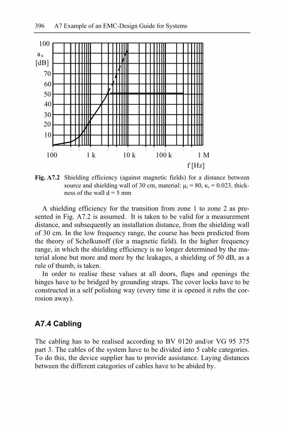
396 A7 Example of an EMC-Design Guide for Systems
100 1 k 10 k 100 k 1 M
10203040506070
100a s[dB]
f [Hz] Fig. A7.2 Shielding efficiency (against magnetic fields) for a distance between
source and shielding wall of 30 cm, material: µr = 80, κr = 0.023, thick-ness of the wall d = 5 mm
A shielding efficiency for the transition from zone 1 to zone 2 as pre-sented in Fig. A7.2 is assumed. It is taken to be valid for a measurement distance, and subsequently an installation distance, from the shielding wall of 30 cm. In the low frequency range, the course has been predicted from the theory of Schelkunoff (for a magnetic field). In the higher frequency range, in which the shielding efficiency is no longer determined by the ma-terial alone but more and more by the leakages, a shielding of 50 dB, as a rule of thumb, is taken.
In order to realise these values at all doors, flaps and openings the hinges have to be bridged by grounding straps. The cover locks have to be constructed in a self polishing way (every time it is opened it rubs the cor-rosion away).
A7.4 Cabling
The cabling has to be realised according to BV 0120 and/or VG 95 375 part 3. The cables of the system have to be divided into 5 cable categories. To do this, the device supplier has to provide assistance. Laying distances between the different categories of cables have to be abided by.

A7.4 Cabling 397
The cables of the system have to be installed on cable trays and the ca-ble trays have to be grounded. The grounding distance between two points on a cable tray should be no larger than 3 m.
Sonar, video and loudspeaker cables have to be installed separately to other cables, with a distance of 50 cm to all other cables. In partitions, where this distance cannot be realised, the cables have to be placed into special shielding tubes; these shielding tubes have to be grounded at both ends. The cables for active and passive sonar have to be installed at a dis-tance of 1 m from each other.
Power supply cables with operating currents of more than 100 A have to be implemented in a multi-core manner and installed in a low stray field arrangement. The power supply of devices (mainly motors), with currents of more than 1000 A, have to be realised by an 8-core cable (4 forward lines and 4 return lines). The phase sequence of the cables has to be ar-ranged as presented in the following sketch:
+ + + +- - - -
The cables of the system have to be divided into 5 cable categories. The example of Fig. A7.3 provides a point of reference for each decision of ca-ble category. Cables of category 1 and category 2, as well as cables of category 3 and category 4, are allowed to be installed together on the same tray. The installation distance between the common category 1/2 and the common category 3/4 must be 200 mm. Category 5 must have a distance of 100 mm to all other categories. The stated distances for the categories are valid for cables laid in parallel over more than 10 m. However, if the cables are laid in parallel over only 5 m, then the separation distance can be reduced by a factor of two.
Crossings of cable trays, which carry different categories of cable, should be arranged at an angle of 90°.
The cross section of three trays filled with cables is presented in Fig. A7.4.
If the distances specified above cannot be realised, then the necessary decoupling must be ensured by use of additional measures. Such additional measures may consist of:
• using cabling with better shielding (lower transfer impedance), • installation of additional plates between the cables of different cate-
gories.
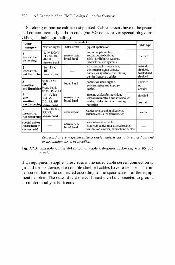
398 A7 Example of an EMC-Design Guide for Systems
Shielding of marine cables is stipulated. Cable screens have to be groun-ded circumferentially at both ends (via VG-cones or via special plugs pro-viding a suitable grounding).
Remark: For every special cable a single analysis has to be carried out and its installation has to be specified.
Fig. A7.3 Example of the definition of cable categories following VG 95 375 part 3
If an equipment supplier prescribes a one-sided cable screen connection to ground for his device, then double shielded cables have to be used. The in-ner screen has to be connected according to the specification of the equip-ment supplier. The outer shield (screen) must then be connected to ground circumferentially at both ends.
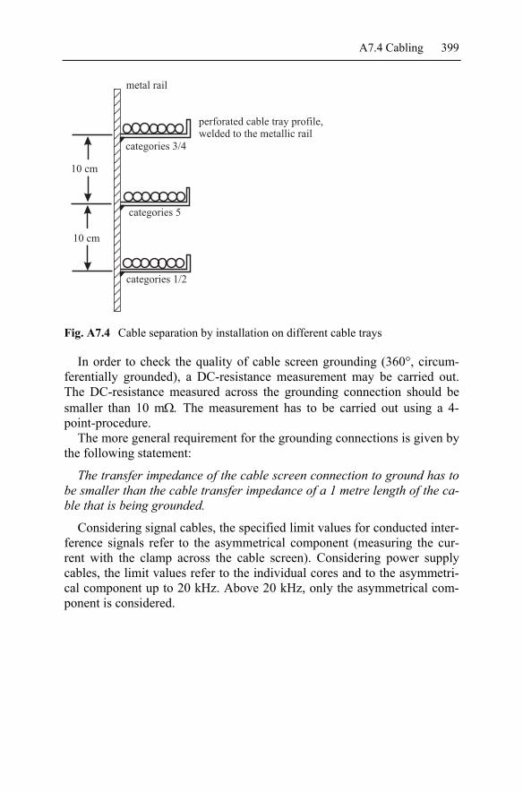
A7.4 Cabling 399
metal rail
perforated cable tray profile,
welded to the metallic rail
categories 3/4
categories 1/2
categories 5
10 cm
10 cm
Fig. A7.4 Cable separation by installation on different cable trays
In order to check the quality of cable screen grounding (360°, circum-ferentially grounded), a DC-resistance measurement may be carried out. The DC-resistance measured across the grounding connection should be smaller than 10 mΩ. The measurement has to be carried out using a 4-point-procedure.
The more general requirement for the grounding connections is given by the following statement:
The transfer impedance of the cable screen connection to ground has to be smaller than the cable transfer impedance of a 1 metre length of the ca-ble that is being grounded.
Considering signal cables, the specified limit values for conducted inter-ference signals refer to the asymmetrical component (measuring the cur-rent with the clamp across the cable screen). Considering power supply cables, the limit values refer to the individual cores and to the asymmetri-cal component up to 20 kHz. Above 20 kHz, only the asymmetrical com-ponent is considered.
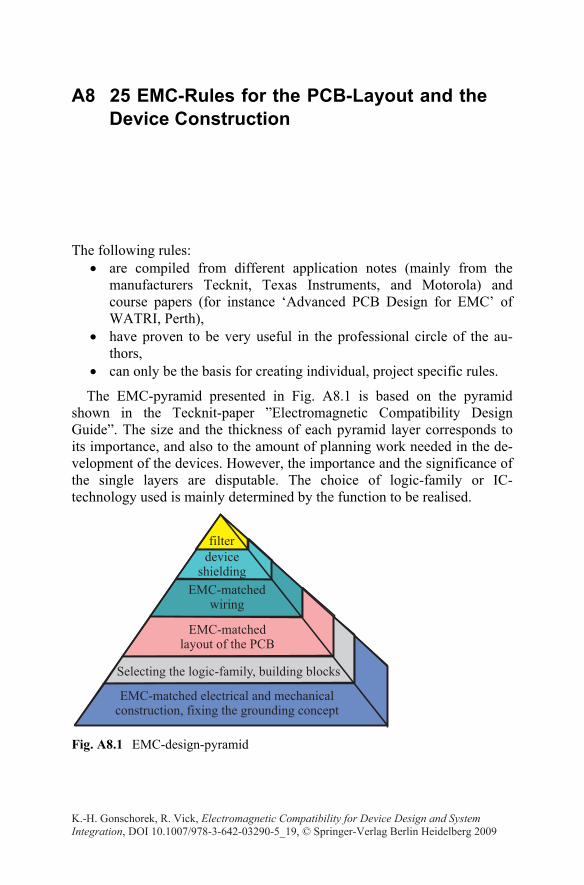
A8 25 EMC-Rules for the PCB-Layout and the Device Construction
The following rules: • are compiled from different application notes (mainly from the
manufacturers Tecknit, Texas Instruments, and Motorola) and course papers (for instance ‘Advanced PCB Design for EMC’ of WATRI, Perth),
• have proven to be very useful in the professional circle of the au-thors,
• can only be the basis for creating individual, project specific rules.
The EMC-pyramid presented in Fig. A8.1 is based on the pyramid shown in the Tecknit-paper ”Electromagnetic Compatibility Design Guide”. The size and the thickness of each pyramid layer corresponds to its importance, and also to the amount of planning work needed in the de-velopment of the devices. However, the importance and the significance of the single layers are disputable. The choice of logic-family or IC-technology used is mainly determined by the function to be realised.
Fig. A8.1 EMC-design-pyramid
K.-H. Gonschorek, R. Vick, Electromagnetic Compatibility for Device Design and System Integration, DOI 10.1007/978-3-642-03290-5_19, © Springer-Verlag Berlin Heidelberg 2009
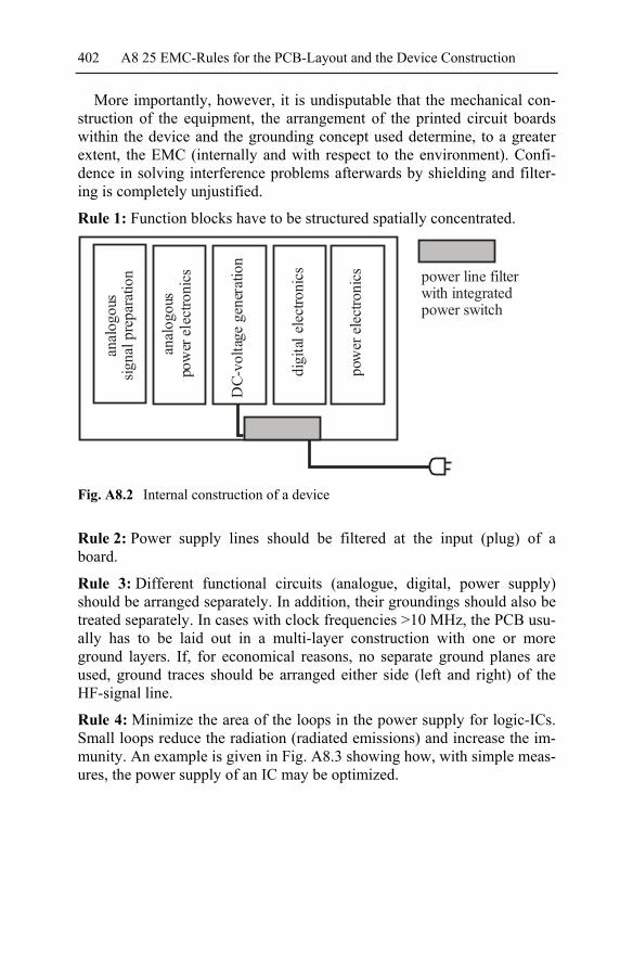
402 A8 25 EMC-Rules for the PCB-Layout and the Device Construction
More importantly, however, it is undisputable that the mechanical con-struction of the equipment, the arrangement of the printed circuit boards within the device and the grounding concept used determine, to a greater extent, the EMC (internally and with respect to the environment). Confi-dence in solving interference problems afterwards by shielding and filter-ing is completely unjustified.
Rule 1: Function blocks have to be structured spatially concentrated.
anal
ogou
ssig
nal p
repa
ratio
n
anal
ogou
spo
wer
elec
troni
cs
digi
tal e
lect
roni
cs
pow
er e
lect
roni
cs
DC-
volta
ge g
ener
atio
n
power line filterwith integratedpower switch
Fig. A8.2 Internal construction of a device
Rule 2: Power supply lines should be filtered at the input (plug) of a board.
Rule 3: Different functional circuits (analogue, digital, power supply) should be arranged separately. In addition, their groundings should also be treated separately. In cases with clock frequencies >10 MHz, the PCB usu-ally has to be laid out in a multi-layer construction with one or more ground layers. If, for economical reasons, no separate ground planes are used, ground traces should be arranged either side (left and right) of the HF-signal line.
Rule 4: Minimize the area of the loops in the power supply for logic-ICs. Small loops reduce the radiation (radiated emissions) and increase the im-munity. An example is given in Fig. A8.3 showing how, with simple meas-ures, the power supply of an IC may be optimized.

A8 25 EMC-Rules for the PCB-Layout and the Device Construction 403
V
V
CC
CC
GND
GND
C
C
a) b)
Fig. A8.3 Power supply to logic IC’s, a) large loop, b) small loop
Rule 5: Avoid current loops. Electrical circuits demand a forward and a re-turn conductor. On a PCB, the forward and its associated return conductor should be arranged close to each other. Two possible signal traces are shown in Fig. A8.4 and Fig. A8.5. As a first order approximation, it can be presumed that the radiation and also the coupling are proportional to the loop area.
I
I
GND
GND
a)
Large loop: Increases the ra-diation, which produces high magnetic fields nearby; the cou-pling in of exter-nal signals is in-creased, hence the immunity is low; increases the impedance for the signal cir-cuit, which makes it unde-fined.
Fig. A8.4 Placement of the return conductor at a great distance from the forward conductor

404 A8 25 EMC-Rules for the PCB-Layout and the Device Construction
I
I
GND
GNDb)
Small loop: Low radiation (interference emissions); small inductive and small capacitive cou-pling; increased immunity; defined impedance for the signal circuit
Fig. A8.5 Placement of the return conductor directly beneath the forward conduc-tor
Rule 6: More generally: Create well defined return paths for currents. The current always flows across the path of lowest impedance (not resistance). Referring to HF-signals, the return path always automatically follows a path near to the forward path. In order to control the radiation (and there-fore also the immunity) defined return paths have to be designed. PCB with ground plane (Fig. A8.6): The return current automatically takes the path of lowest impedance. Also see Fig. 2.2 for this effect.
GND
GND
GND
GND
Fig. A8.6 Return current conductor provided by the ground plane
The best return path is created using an uninterrupted ground plane. The coupling between the two circuits via the impedance of the return path is normally very low.
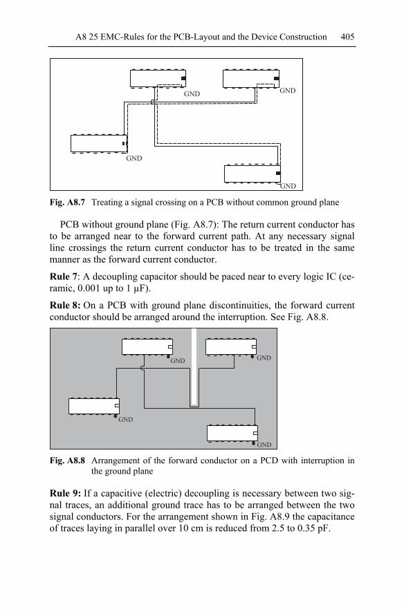
A8 25 EMC-Rules for the PCB-Layout and the Device Construction 405
GND
GND
GND
GND
Fig. A8.7 Treating a signal crossing on a PCB without common ground plane
PCB without ground plane (Fig. A8.7): The return current conductor has to be arranged near to the forward current path. At any necessary signal line crossings the return current conductor has to be treated in the same manner as the forward current conductor.
Rule 7: A decoupling capacitor should be paced near to every logic IC (ce-ramic, 0.001 up to 1 µF).
Rule 8: On a PCB with ground plane discontinuities, the forward current conductor should be arranged around the interruption. See Fig. A8.8.
GND
GND
GND
GND
Fig. A8.8 Arrangement of the forward conductor on a PCD with interruption in
the ground plane
Rule 9: If a capacitive (electric) decoupling is necessary between two sig-nal traces, an additional ground trace has to be arranged between the two signal conductors. For the arrangement shown in Fig. A8.9 the capacitance of traces laying in parallel over 10 cm is reduced from 2.5 to 0.35 pF.
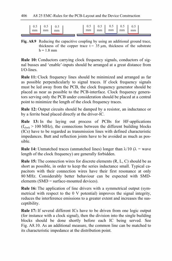
406 A8 25 EMC-Rules for the PCB-Layout and the Device Construction
Fig. A8.9 Reducing the capacitive coupling by using an additional ground trace,
thickness of the copper trace t = 35 µm, thickness of the substrate h = 1.8 mm
Rule 10: Conductors carrying clock frequency signals, conductors of sig-nal busses and ‘enable’-inputs should be arranged at a great distance from I/O-lines.
Rule 11: Clock frequency lines should be minimized and arranged as far as possible perpendicularly to signal traces. If clock frequency signals must be led away from the PCB, the clock frequency generator should be placed as near as possible to the PCB-interface. Clock frequency genera-tors serving only the PCB under consideration should be placed at a central point to minimize the length of the clock frequency traces.
Rule 12: Output circuits should be damped by a resistor, an inductance or by a ferrite bead placed directly at the driver-IC.
Rule 13: In the laying out process of PCBs for HF-applications (fclock > 100 MHz), the connections between the different building blocks (ICs) have to be regarded as transmission lines with defined characteristic impedances. Butt and reflection joints have to be avoided as much as pos-sible.
Rule 14: Unmatched traces (unmatched lines) longer than λ/10 (λ = wave length of the clock frequency) are generally forbidden.
Rule 15: The connection wires for discrete elements (R, L, C) should be as short as possible, in order to keep the series inductance small. Typical ca-pacitors with their connection wires have their first resonance at only 80 MHz. Considerably better behaviour can be expected with SMD-elements (SMD = surface-mounted devices).
Rule 16: The application of line drivers with a symmetrical output (sym-metrical with respect to the 0 V potential) improves the signal integrity, reduces the interference emissions to a greater extent and increases the sus-ceptibility.
Rule 17: If several different ICs have to be driven from one logic output (for instance with a clock signal), then the division into the single building blocks should be done shortly before each IC being served. See Fig. A8.10. As an additional measure, the common line can be matched to its characteristic impedance at the distribution point.

A8 25 EMC-Rules for the PCB-Layout and the Device Construction 407
GN
D
GND
GND
GND
Fig. A8.10 Servicing several building blocks with the same clock signal
Rule 18: Input, as well as load capacitances should be as low as possible. Through this measure the charging currents for the state change are re-duced. Therefore, the radiation of magnetic fields and the return currents in the ground are decreased.
Rule 19: Beware of demodulation problems within analogue circuits. Most EMC-problems within analogue semiconductor components are caused by demodulation of radio frequency signals. In order to prevent demodulation, analogue circuits must operate in a stable and linear manner, even when subject to interference from high frequency disturbing signals. This can only be achieved by use of an input filter or a suitable feedback circuit.
Rule 20: Similar to the procedure at the system level, all lines (here the wiring) of the devices should be separated into categories determined by the signals they carried. A specific wiring path should be chosen for each category. The categories should be arranged with the largest possible dis-tance to each other, near to the equipment ground, and in a sequence from sensitive/not disturbing up to not sensitive/highly disturbing; see Fig. A8.2.
Rule 21: A low-stray field arrangement can easily be realised through use of multi-wire flat ribbon cables. Flat ribbon cables have to be installed di-rectly on the equipment ground. If installation directly on the equipment ground results in an intolerable extension or no equipment ground is avail-able along the run of the cable, then a copper foil fixed along the underside of the multi-wire flat ribbon cable may provide a considerable improve-ment (imaging principle).
Rule 22: From the view point of EMC, no passive conductors exist within an electronic device.
408 A8 25 EMC-Rules for the PCB-Layout and the Device Construction
Rule 23: If possible, the power-switch should be integrated into the line filter. The operation indicator has to be realised by a LED (light emitting diode) on the low voltage side.
Rule 24: The following shielding rules should be obeyed when defining the shielding box:
• Low frequency electric fields (on equipment level up to 1 MHz) are easily shielded (using thin-walled metal housings or plastic housings with metallization).
• Low frequency magnetic fields (on equipment level up to 1 MHz) demand thick-walled metal housings (the fields of power frequen-cies may be lowered by highly permeable materials).
• The leakages (holes, slots) determine the shielding behaviour more and more with increasing frequency. The leakage with the greatest extension determines the degree of reduction in the total shielding efficiency. Starting with an extension of a leakage of 30 me-tre/f[MHz] (λ/10), a shielding efficiency of 0 dB can be expected.
• Assuming the areas must be equal, then a lot of small holes (for in-stance for air ventilation) are essentially better than a few large holes (the greatest extension in one direction determines the shield-ing efficiency).
Rule 25: The goal of all EMC-measures in developing a piece of equip-ment should consist of toughening up the electronics of the equipment so that the interference emission requirements, and also the immunity con-straints of the environment ‘household, light industry’ (EN 61000-3-3, EN 61000-3-1), are fulfilled without any additional shielding housing.
Further information
The following manufacturer’s application notes contain a lot of useful EMC hints and rules for the construction of analogue and digital printed boards. Developers and designers of electronic circuits and equipment are advised to read these notes:
Motorola: “Designing for Board Level Electromagnetic Compatibility”, AN 2321/D, 2002, “Noise Reduction Techniques for Microcontroller-Based Systems”, AN 1705, 1999
Teknit: “Electromagnetic Compatibility Design Guide”, 1998
Texas Instruments: “Printed-Circuit-Board Layout for Improved Elec-tromagnetic Compatibility”, SDYA011, Oct. 1996 “PCB Design Guide-lines For Reduced EMI”, SZZA009, Nov. 1999

A9 Easy-to-use Procedure for Predicting the Cable Transfer Impedance
A model was described in chapter 7.6.3 for analysing the coupling of elec-tromagnetic signals into a cable. This model is based on the assumption that first, the current on the screen of a shielded cable has to be predicted and second, the coupling-in is calculated using transmission line theory with the basic approach of distributed sources along the cable. Assuming that the current is known, the problem reduces to solving the equations of transmission line theory. Fig. A9.1, which is identical to Fig. 7.43, presents the process of coupling once again.
x
x
x
xx
I1
I2
I3
I4
I5
dU3
dU1
dU2
dUN
l
IL2
IL1
Z UL1
ZL2
UL2L1
~ ~ ~ ~ ~ ~ ~
Ii
Ui = Z
T z. .’ Fig. A9.1 Model for predicting the coupling into a shielded cable
The voltages across the load impedances ZL1 and ZL2 can be predicted by using Eqs. (A9.1) to (A9.5).
K.-H. Gonschorek, R. Vick, Electromagnetic Compatibility for Device Design and System Integration, DOI 10.1007/978-3-642-03290-5_20, © Springer-Verlag Berlin Heidelberg 2009

410 A9 Easy-to-use Procedure for Predicting the Cable Transfer Impedance
( ) ( )[ ] ,sinhcosh' 20
11 dzzlZzlIZ
DZU L
l
TL
L −+−∫−= γγΓ (A9.1)
[ ]
( ) ( )
212
0
21 2 1 2
' cosh sinh ,
cosh sinh ,
lL
T LL
L L L L
ZU Z I z Z z dzD
D Z Z l Z Z l
γ γ
γ γ
= Γ +
= Γ + Γ + Γ +
∫ (A9.2)
( ) ( )[ ] ∑ −+−−=i
iLiiL
L zlZzlUD
ZU ,sinhcosh 21
1 γγΓΔ (A9.3)
[ ] ∑ +=i
iLiL
L zZzUD
ZU ,sinhcosh 112
2 γγΓΔ (A9.4)
,' zZIU kii ΔΔ = (A9.5)
Γ = characteristic impedance, γ = propagation constant of the cable.
The equations for the voltages coupled-in across the load impedances (for instance across ZL2) can be written in the following form:
021' UFFZU TL = . (A9.6)
Here, F1 represents a complicated function for the coupling process out-side of the cable.
F2 describes the relations inside the cable (transmission line theory un-der the basic approach of distributed sources).
'TZ is the cable transfer impedance and U0 is the voltage responsible for the electromagnetic radiation process in the outer region of the cable.
Rearranging Eq. (A9.6) for 'TZ yields a relation to allow this quantity to be predicted:
.11
0210
'
S
LLT FU
UFFU
UZ == (A9.7)
If we start from the assumption that the functions F1 and F2 (FS = F1 F2) can be calculated using a computer program, only the task of predicting the relation UL/U0 remains. This can, for instance, be performed by measure-ment using a network analyser, which is the best device to use as it pro-

A9 Easy-to-use Procedure for Predicting the Cable Transfer Impedance 411
vides the highest sensitivity. The function FS, meaning the coupling factor, within a defined measuring arrangement depends on:
• The geometrical relations • The characteristic impedance of the cable under investigation • The radius R0 • The dielectric constant, εr, inside the cable
To clarify: An arrangement of a cable is constructed, which can be eas-ily analysed using a computer program; a semi-circle above conducting ground, for instance. Such an arrangement is presented in Fig. A9.2. The cable is represented by a cylindrical conductor. The arrangement is excited by a voltage U0 at a suitable point. The current distribution on the cable screen is then used as an output from the computer program. Using the above mentioned Eqs. (A9.1) to (A9.5) the voltage coupled into the cable is now calculated. If, however, the arrangement is excited, analysed and the voltage UL measured, then the complex cable transfer impedance can be predicted. The procedure works well starting at approximately 100 kHz. Below this frequency, it is possible to take the DC-resistance per metre of the cable coat to obtain the cable transfer impedance.
U U U0
0
2 LL2
L1
R
R2
Z
Z
I(z)
=
Fig. A9.2 Arrangement for predicting the complex cable transfer impedance
Proceeding one step further and defining a fixed test arrangement, then the functions F1 and F2, hence the coupling factor FS = F1 *F2, need only be calculated once. They are, in a manner of speaking, geometrical constants. The relation UL/U0 determines the complex cable transfer impedance. The coupling factor FS for Γ = 50 Ω, εr = 2.3 and R = 25 cm is shown in Fig. A9.3.
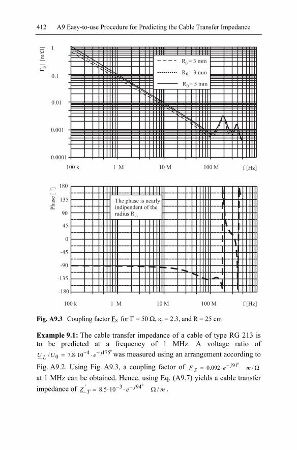
412 A9 Easy-to-use Procedure for Predicting the Cable Transfer Impedance
R = 5 mm
R = 3 mm
R = 3 mm
0
0
0
100 k 1 M 10 M 100 M f [Hz]
0.0001
0.001
0.01
0.1
1
|F|
[m/
]
S
100 k 1 M 10 M 100 M f [Hz]
Phase
[]
0
-180
-135
-90
-45
45
0
90
135
180
0
The phase is nearly
indipendent of the
radius R
Fig. A9.3 Coupling factor FS for Γ = 50 Ω, εr = 2.3, and R = 25 cm
Example 9.1: The cable transfer impedance of a cable of type RG 213 is to be predicted at a frequency of 1 MHz. A voltage ratio of
017540 108.7/ j
L eUU −− ⋅⋅= was measured using an arrangement according to
Fig. A9.2. Using Fig. A9.3, a coupling factor of Ω⋅= − /092.0091 meF j
S at 1 MHz can be obtained. Hence, using Eq. (A9.7) yields a cable transfer impedance of meZ j
T /105.80943' Ω⋅⋅= −− .

A9.1 Predicting the voltage ratio with help of an oscilloscope 413
A9.1 Predicting the voltage ratio with help of an oscilloscope
The measuring arrangement for predicting the voltage ratio 0/UU L using a dual-channel oscilloscope is presented in Fig. A9.4.
Choosing equal cable lengths, l1 and l2, and triggering the oscilloscope by the feeding signal (feeding voltage), allows the image on the oscillo-scope to be directly evaluated in order to predict the voltage ratio. It is as-sumed that both measuring cables are of the same type.
U0 U2
0
L1
R
R2
Z = 50
I(z)
50 50
oscilloscope
signal
generator
1 2I I
Fig. A9.4 Measuring the voltage ratio with help of an oscilloscope
The picture on the oscilloscope for the measurement of a cable RG 58 at 10 MHz is shown in Fig. A9.5.
U U2
U[V
]L
U[V
]0
0
t
t [ns]
0 50 100 150
4
3
2
1
0
-1
-2
-3
-4
0.004
0.002
0
-0.002
-0.004
Fig. A9.5 Picture on the oscilloscope investigating a RG 58 at 10 MHz
The cable parameters are:

414 A9 Easy-to-use Procedure for Predicting the Cable Transfer Impedance
• Outer radius of the screen R0 1.75 mm • Characteristic impedance Γ 50 Ω • Relative permeability εr 2.3
The following values can be taken from the oscilloscope’s picture: U0 = 3.8 V UL = 2.7 mV Δt = 56 ns
Fig. A9.6 Transfer impedance of the cable RG 58, predicted by an oscilloscope
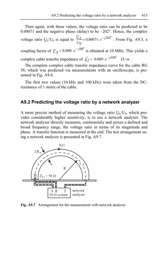
A9.2 Predicting the voltage ratio by a network analyzer 415
Then again, with these values, the voltage ratio can be predicted to be 0.00071 and the negative phase (delay) to be –202°. Hence, the complex
voltage ratio UL/U0 is equal to .00071.00202
0
jL eUU −⋅= From Fig. A9.3, a
coupling factor of 098008.0 j
S eF −⋅= is obtained at 10 MHz. This yields a
complex cable transfer impedance of meZ jT /089.0
0104' Ω⋅= − . The complete complex cable transfer impedance curve for the cable RG
58, which was predicted via measurements with an oscilloscope, is pre-sented in Fig. A9.6.
The first two values (10 kHz and 100 kHz) were taken from the DC-resistance of 1 metre of the cable.
A9.2 Predicting the voltage ratio by a network analyzer
A more precise method of measuring the voltage ratio UL/U0, which pro-vides considerably higher sensitivity, is to use a network analyser. The network analyser directly measures, continuously and across a defined and broad frequency range, the voltage ratio in terms of its magnitude and phase. A transfer function is measured at the end. The test arrangement us-ing a network analyser is presented in Fig. A9.7.
0
L1
R
R2
Z = 50
I(z)
network
analyzer
S R T
50 system
Fig. A9.7 Arrangement for the measurement with network analyser

416 A9 Easy-to-use Procedure for Predicting the Cable Transfer Impedance
f [MHz]
0.1 1 10 100 1k
0.01
0.001
0.0001
|/U
|U
L0
f [MHz]
0.1 1 10 100 1k
Phase
[]
0
-180
-135
-90
-45
45
0
90
135
180
Fig. A9.8 Voltage ratio UL/U0 for the cable RG 213 obtained using a network
analyser
The output S of the network analyser serves as the signal generator. The input R measures the signed fed into the outer circuit and the input T measures the signal coupled into the cable. The network analyser relates the measured value at input T to the value measured at R and thereby cal-culates the complex transfer function. Preliminary calibration eliminates the magnitude and phase errors introduced due to the measurement cables.
The voltage ratio UL/U0 for the cable RG 213 is shown in Fig. A9.8 as it has been obtained from the use of a network analyser. The cable RG 213 has the following parameters:
Outer radius of the screen R0 = 4 mm Characteristic impedance Γ = 50 Ω Relative permeability εr = 2.3
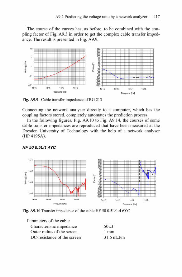
A9.2 Predicting the voltage ratio by a network analyzer 417
The course of the curves has, as before, to be combined with the cou-pling factor of Fig. A9.3 in order to get the complex cable transfer imped-ance. The result is presented in Fig. A9.9.
Frequenz [Hz]
1e+5 1e+6 1e+7 1e+8
Betra
g[Ω
/m]
,001
,01
,1
1
10
Frequenz [Hz]
1e+5 1e+6 1e+7 1e+8
Phas
e [°
]
-180-165-150-135-120-105-90-75-60-45-30-15
0153045607590
105120135150165180
Fig. A9.9 Cable transfer impedance of RG 213
Connecting the network analyser directly to a computer, which has the coupling factors stored, completely automates the prediction process.
In the following figures, Fig. A9.10 to Fig. A9.14, the courses of some cable transfer impedances are reproduced that have been measured at the Dresden University of Technology with the help of a network analyser (HP 4195A).
HF 50 0.5L/1.4YC
Frequenz [Hz]
1e+5 1e+6 1e+7 1e+8
Betra
g[Ω
/m]
1e-4
1e-3
1e-2
1e-1
Frequenz [Hz]
1e+5 1e+6 1e+7 1e+8
Phas
e [°
]
-180-165-150-135-120-105
-90-75-60-45-30-15
0153045607590
105120135150165180
Fig. A9.10 Transfer impedance of the cable HF 50 0.5L/1.4 6YC
Parameters of the cable Characteristic impedance 50 Ω Outer radius of the screen 1 mm DC-resistance of the screen 31.6 mΩ/m

418 A9 Easy-to-use Procedure for Predicting the Cable Transfer Impedance
RG 174 /U
Frequenz [Hz]
1e+5 1e+6 1e+7 1e+8
Betra
g[Ω
/m]
,001
,01
,1
1
10
Frequenz [Hz]
1e+5 1e+6 1e+7 1e+8
Phas
e [°
]
-180-165-150-135-120-105-90-75-60-45-30-15
0153045607590
105120135150165180
Fig. A9.11 Transfer impedance of the cable RG 174 /U
Parameters of the cable Characteristic impedance 50 Ω Outer radius of the screen 1 mm DC-resistance of the screen 37.5 mΩ/m
RG 214 /U
Frequenz [Hz]
1e+5 1e+6 1e+7 1e+8
Betra
g[Ω
/m]
1e-4
1e-3
1e-2
1e-1
Frequenz [Hz]
1e+5 1e+6 1e+7 1e+8
Phas
e [°
]
-180-165-150-135-120-105-90-75-60-45-30-15
0153045607590
105120135150165180
Fig. A9.12 Transfer impedance of cable RG 214 /U
Parameters of the cable Characteristic impedance 50 Ω Outer radius of the screen 4.4 mm DC-resistance of the screen 4.6 mΩ/m

A9.2 Predicting the voltage ratio by a network analyzer 419
RG 217 /U
Frequenz [Hz]
1e+5 1e+6 1e+7 1e+8
Betra
g[Ω
/m]
1e-6
1e-5
1e-4
1e-3
1e-2
1e-1
Frequenz [Hz]
1e+5 1e+6 1e+7 1e+8
Phas
e [°
]
-180-165-150-135-120-105-90-75-60-45-30-15
0153045607590
105120135150165180
Fig. A9.13 Transfer impedance of the cable RG 217 /U
Parameters of the cable Characteristic impedance 50 Ω Outer radius of the screen 5.05 mm DC-resistance of the screen 2.1 mΩ/m
RG 223 /U
Frequenz [Hz]
1e+5 1e+6 1e+7 1e+8
Bet
rag[
Ω/m
]
1e-4
1e-3
1e-2
1e-1
Frequenz [Hz]
1e+5 1e+6 1e+7 1e+8
Phas
e [°
]
-180-165-150-135-120-105-90-75-60-45-30-15
0153045607590
105120135150165180
Fig. A9.14 Transfer impedance of the cable RG 223 /U
Parameters of the cable Characteristic impedance 50 Ω Outer radius of the screen 2.1 mm DC-resistance of the screen 7.45 mΩ/m
Remark: The measurement arrangements, diagrams and results of this annex chapter were created to a large extent by Dr. Tiedemann in connec-tion with his PhD-work, [TIE01]. Additional examples and measurement curves are given in the publication [TI/GO98].

A10 Capacitances and Inductances of Common Interest
Conductor/ Construction
Inductance (per metre)
Capacitance (per metre)
1. Plane / Plane
d
d
AC ⋅=ε
2. Layered dielectric
a a1
1
2
2
r
r
01221
21 εεε
εε⋅
⋅+⋅⋅⋅
=aa
ACrr
rr
n- layers
rn
n
r
aaA
C
εε
ε
++
⋅=
1
1
0
3. Concentric spheres
Rar
Ri
ia
ia
RRRRC
−⋅⋅⋅
⋅=πε 4
Sphere against an infi-nitely far away coun-terpart
RC ⋅⋅⋅= πε 4
K.-H. Gonschorek, R. Vick, Electromagnetic Compatibility for Device Design and System Integration, DOI 10.1007/978-3-642-03290-5_21, © Springer-Verlag Berlin Heidelberg 2009

422 A10 Capacitances and Inductances of Common Interest
4. Sphere / Plane
R
b
)2
1(4b
RRC⋅
+⋅⋅⋅⋅= πε
5. Sphere / Sphere – Sphere spark gap
b
R R
bRforbRRC
RbRbbRbRRC
<<+⋅⋅⋅⋅=
⋅−−⋅−⋅
+⋅⋅⋅⋅=
)1(2
)()(1(2 22
22
πε
πε
6. Concentric cylinders
Ri
Ra
i
a
RRnlL
πμ⋅
=2
' i
a
RRnl
C πε ⋅⋅=
2'
7. Elliptical cable
a2
a1
b2b1
11
22
2'
babanlL
++
⋅=
πμ
11
22
2'
babanl
C
++⋅⋅
=πε
8. Layered dielectric within a cylindrical capacitor
R1
R2
R3
R0
r1
r2
r3
nr
n
n
r
RRnl
RRnl
lC
εε
πε
1
2
1
0
1
0
−++
⋅⋅⋅=

A10 Capacitances and Inductances of Common Interest 423
9. Eccentric cylinders with 2 axes
R
Ri
ad
)4)(
4)((
2'
222222222
222222222
aiaia
aiaia
i
a
RddRRdRR
RddRRdRRRRnl
C
−+−++−
−+−+−−⋅
⋅⋅=
πε
ia
a
RRdRnlL
⋅−
⋅=
22
2'
πμ
10. Two-conductor cable
rr
R
d
)4()4('
22
22
dRrdRdnlL
+⋅⋅−⋅⋅
=πμ 2 2
2 2
'(4 )( 4 )
Cd R d
lnr R d
ε π⋅=
⋅ ⋅ −⋅ ⋅ +
11. Cylindrical conductor / Plane
)1)((
2'2 −+
⋅⋅=
Rb
Rbnl
C πε
)1)((2
' 2 −+⋅
=Rb
RbnlL
πμ
R
b
R
bnlL ⋅⋅
=2
2'
πμ 2 22
'2
C für R bb
lnR
ε π⋅ ⋅= <<
⋅
12. Two parallel strip lines
h
d
hdL ⋅= μ'
´h
Cd
ε= ⋅
for d>>h

424 A10 Capacitances and Inductances of Common Interest
13. Vertical antenna
R
h
2
lhlh
Rlnl
lC
344
2
+⋅+⋅
⋅
⋅⋅⋅=
πε
Rlnl
lC
Rlnl
lC
⋅
⋅⋅⋅=
⋅⋅⋅=
3
22 πεπε
0→∞→ hforhfor
14. Horizontal antenna
R
h
2
⎥⎦
⎤⎢⎣
⎡−+
⋅⋅
⋅⋅
⋅⋅⋅=
11)4(4
2
2
lh
hl
Rlnl
lC πε
142
2<<
⋅⋅⋅⋅⋅
=l
hfor
Rhnl
lC πε
15. Two parallel wires of finite length
d
2r
22
22
22
)2(
)2(
)2(
lrfor
ldl
ldlrlnl
lC
<<
++
−+⋅
⋅⋅=
πε
16. Parallel cylindrical conductors
21
'rr
dnlL⋅
=πμ
mrrdmrrdnl
C
−−−+−−
⋅⋅=
212
2
212
2
)()(
2' πε
d
r2 r1
22
21
2222
21 4)( rrdrrmwith −−+=
21
21
2 ,2' rrdfür
rrdnl
C >>
⋅
⋅⋅=
πε

A10 Capacitances and Inductances of Common Interest 425
17. Two cylindrical conductors above ground
a) d
h2r
2)2(1
2'
dhr
hnlC
+⋅
⋅=
πε
2)2(1
2'
dhr
hnlL+⋅
=πμ
b)
h
2r
a/2
a/2
rh
aanl
C2)
2(1
'−⋅
⋅=
πε
rh
aanlL
2)2
(1'
−⋅=πμ
c)
a
2h1
h2r
21
2
41
'
hhar
anlC
⋅⋅+⋅
⋅=
πε
21
2
41
'
hhar
anlL
⋅⋅+⋅
=πμ
18. Conductor between 2 planes
2h/2
h/2
r
ππμ
⋅⋅=
rhnlL 2
2'
π
πε
⋅
⋅⋅=
rhnl
C22'
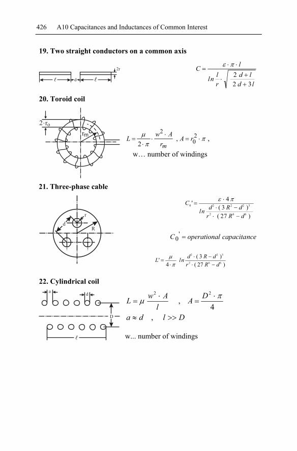
426 A10 Capacitances and Inductances of Common Interest
19. Two straight conductors on a common axis
d
2r
ldld
rlnl
lC
322
++
⋅
⋅⋅=
πε
20. Toroid coil
rm
2.ro
ππμ
⋅=⋅
⋅⋅
= 20
2,
2rA
rAwL
m,
w… number of windings
21. Three-phase cable
d
r
R
)72()3(
4'
662
32220
dRrdRdnl
C
−⋅−⋅
⋅=
πε
ncecapacitaloperationaC ='0
)27()3(
4'
662
322
dRrdRdnlL−⋅
−⋅⋅
=πμ
22. Cylindrical coil
D
ad
Dlda
DAl
AwL
>>≈
⋅=
⋅=
,4
,22 πμ
w... number of windings
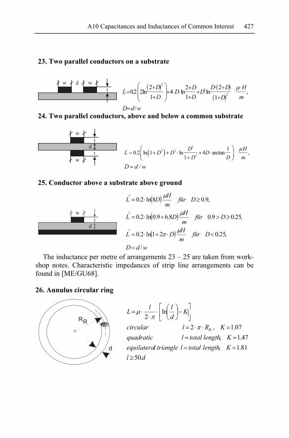
A10 Capacitances and Inductances of Common Interest 427
23. Two parallel conductors on a substrate
dw w
t( ) ( )
( )
2' 2
2
2 220.2 2ln 4 ln ln ,
1 1 1
/
D D DD HL D D
D D mD
D d w
μ+ ⋅ ++ ⋅= + ⋅ ⋅ +
+ + +
=
⎛ ⎞⎜ ⎟⎝ ⎠
24. Two parallel conductors, above and below a common substrate
d
w
w
t
t ( )2
' 2 22
10.2 ln 1 ln 4 arctan ,
1
/
D HL D D D
D D m
D d w
μ= + + ⋅ + ⋅
+
⎛ ⎞⎜ ⎟⎝ ⎠
=
25. Conductor above a substrate above ground
d
w
t
( )
( )
( )wdD
DfürmHDL
DfürmHDL
DfürmHDL
/
,25.021ln2.0
,25.09.08.69.0ln2.0
,9.08ln2.0
'
'
'
=
<⋅+⋅=
≥>+⋅=
≥⋅=
μπ
μ
μ
The inductance per metre of arrangements 23 – 25 are taken from work-shop notes. Characteristic impedances of strip line arrangements can be found in [ME/GU68].
26. Annulus circular ring
RR
d
dl
KlengthtotalltrianglelequilateraKlengthtotallquadratic
KRlcircular
KdllL
R
5081.1,47.1,
07.1,2
ln2
≥====
=⋅⋅=
⎥⎦
⎤⎢⎣
⎡−⎟⎠⎞
⎜⎝⎛⋅
⋅⋅=
ππ
μ
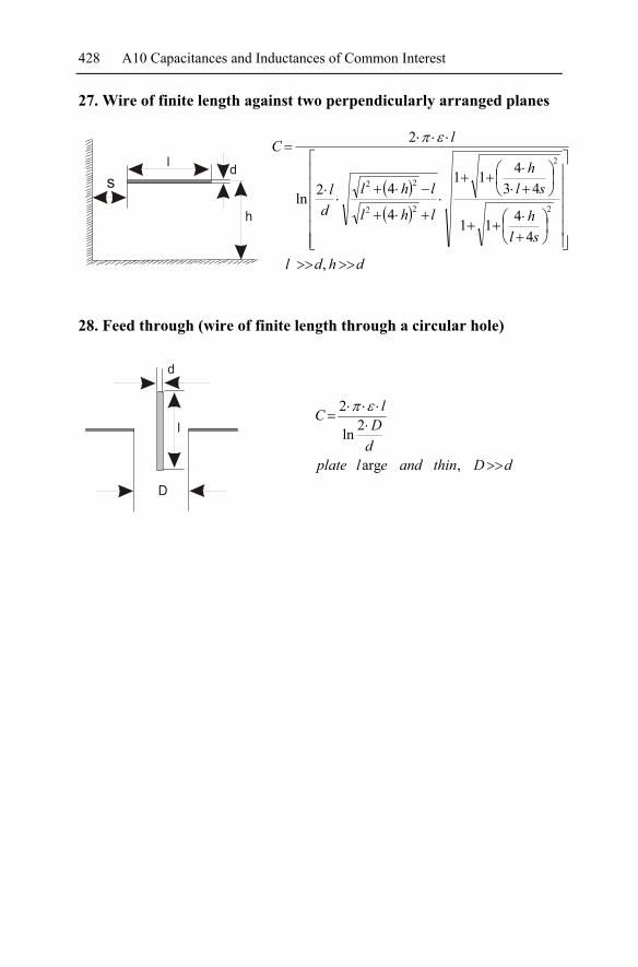
428 A10 Capacitances and Inductances of Common Interest
27. Wire of finite length against two perpendicularly arranged planes
ls
d
h
( )( )
dhdl
slh
slh
lhl
lhld
l
lC
>>>>⎥⎥⎥⎥⎥⎥
⎦
⎤
⎢⎢⎢⎢⎢⎢
⎣
⎡
⎟⎠⎞
⎜⎝⎛+⋅
++
⎟⎠⎞
⎜⎝⎛
+⋅⋅
++⋅
+⋅+
−⋅+⋅
⋅
⋅⋅⋅=
,
4411
43411
4
42ln
2
2
2
22
22
επ
28. Feed through (wire of finite length through a circular hole)
l
d
D
dDthinandelplatedD
lC
>>
⋅⋅⋅⋅
=
,arg
2ln
2 επ

A11 Reports of Electromagnetic Incompatibilities
The spectrum of electromagnetic incompatibilities is as large as the spec-trum utilising the electric, magnetic, and electromagnetic effects. In order to demonstrate to the reader the large variety of possible interferences, the following paragraphs present some inference case descriptions and self-experienced incompatibilities. Furthermore, they aim to demonstrate ways to analyse and contemplate special interrelations for solving electromag-netic incompatibilities.
Tony Dibiase reported in ITEM UPDATE 2001:
1. Problem In March 1998, when a TV station in Austin, Texas, began testing its new Digital Television System (DTV), a nearby hospital’s wireless telemetry system became nearly useless.
Cause: The hospital’s telemetry system and the TV station’s DTV sig-nals both occupied the same frequency band.
2. Problem A magnetic resonance imaging (MRI) system facility experienced mal-functions in the MRI equipment’s operation at about the same time each day.
Cause: A large refuse truck made a pickup each day at the hospital, at a location adjacent to the MRI facility. The refuse truck represented a sig-nificant metal mass that distorted the MRI’s magnetic field.
3. Problem His pacemaker malfunctioned when a man leaned against a pylon of a de-partment store’s Electronic Article Surveillance (EAS) system for several minutes.
Cause: The frequency and power levels of the EAS emissions interfered with the proper operation of the pacemaker.
4. Problem A student wearing a hearing aid experienced discomfort (jaw vibrations) when entering a classroom that had recently been retrofitted with a new high efficiency lighting system. K.-H. Gonschorek, R. Vick, Electromagnetic Compatibility for Device Design and System Integration, DOI 10.1007/978-3-642-03290-5_22, © Springer-Verlag Berlin Heidelberg 2009

430 A11 Reports of Electromagnetic Incompatibilities
Cause: Her hearing aid amplified the 27 kHz signal emitted from the new lighting system’s electronic circuit.
5. Problem Some types of cell phones, primarily digital types, have been reported to have caused malfunctions to pacemakers.
Cause: Due to their small size, cell phones are sometimes placed in a shirt pocket of a person who has a pacemaker, which is close the person’s heart. The likelihood of EMI interactions is greatly increased by the close proximity of the cell phone’s antenna to the pacemaker electronics.
6. Problem It was reported that medical equipment inside an ambulance shut down be-cause of an EMI interaction with the ambulance communications equip-ment.
Cause: The mobile transmitter in the ambulance created a field in ex-cess of 20 volts per metre, which exceeded the immunity threshold of the equipment.
Self-experienced EMI (electromagnetic incompatibilities)
1. Problem The demodulated signal of a medium wave radio station could be clearly heard coming out of some EEG-equipment (EEG = electroencephalo-gram).
Reason: A field strength of appr. 1 V/m at 1 MHz existed at the operat-ing position of the EEG-equipment that was being produced by a near-by medium wave radio station.
Solution: Forcing the manufacturer to satisfy the requirement to increase the immunity.
2. Problem The monitors inside a control room for observing and controlling the tram operation of a city showed only unfocused and shaking readings (pictures).
Reason: The switching equipment, in which currents of up to 4 kA at 16 2/3 Hz were flowing, was located below the control room.
Solution: The monitors were shielded using double-walled housings made of mumetal.
3. Problem Within a heating control system (gas) a relay was switching in time with the Morse characters of a radio amateur.
Reason: Operation of the transmitter using a whip antenna without a counterpoise.

A11 Reports of Electromagnetic Incompatibilities 431
Solution: Changing the unsymmetrically operating antenna (whip a-gainst undefined ground) to a symmetrically driven one (Yagi) solved the problem.
4. Problem Interference signals occurred in a radio observation station, which, in the beginning, could not be indentified.
Reason: An electronic device working at a clock frequency of 4 MHz with insufficient suppression was identified after some on/off-switchings.
Solution: Replacement of the electronic device.
5. Problem In a computer cabinet, slight, but unacceptable movements occurred on some monitors in a certain region of the room.
Reason: A defect in a heating control system was leading to currents of approximately 30 A to ground.
Solution: Repair of the heating system solved the problem.
6. Problem Sporadically shutdowns of a computer system occurred wthin a room for controlling and steering the melting of aluminium.
Reason: Below the control room, the current for the melting process was rectified with total amplitudes up to 120 kA. Field strength values of more than 500 A/m could be measured at the position of the computer system.
Solution: Increasing the distance between the current carrying conduc-tors and the PC-system.
7. Problem On a certain wall, at certain times, within a sales outlet for radio and TV equipment, very strong distortions of the TV pictures occurred.
Reason: The interference source was detected very quickly. It was the diathermy equipment used in a nearby doctor’s surgery.
Solution: The problem has been solved by organisational measures (agreement about operation times).
8. Problem Sporadic, minor, but inconvenient picture interferences occurred on some monitors placed near the window to the street of an architect’s office. The closest tram rails were at a distance of at least 200 m from the office.
Reason: After half an hour of searching the interference source was de-tected and located below the pavement in front of the building. An inquiry at the transport services made the situation clear. Running at a depth of 80 cm below the pavement there was a conductor for emergency feeding and, at that point in time, it was in operation.

432 A11 Reports of Electromagnetic Incompatibilities
Solution: The interferences had been accepted during the period of emergency feeding.
9. Problem A laser writing system within a very rough industrial environment dis-
played sporadic blackouts. It was assumed to be an EMC-problem. Reason: It transpired that the oscillator for driving the writing head of
the system simply showed a very strong temperature dependency.
10. Problem During a normal quality check, some electronic control units showed con-siderable limit overshoots, although up to that date the limits had been met. The developing engineers denied any change in the construction or layout.
Reason: Change of supplier of the logic integrated circuits. Solution: Using only the IC’s provided by the first supplier.
11. Problem An automobile could not be restarted within a shortwave transmission plant during a measurement action.
Reason: No sufficient immunity of the automobile’s ignition system a-gainst the given fields.
Solution: Moving the automobile by 10 m away from a nearby antenna made the ignition system work again. The situation was reproducible.
Report from the Falkland war
In 1982, Great Britain lost its destroyer HMS Sheffield during action with Argentina in the Falkland war. The radio installation for communication with Great Britain did not work sufficiently whilst the ships-own anti-rocket-detection-system was being operated as a result of electromagnetic interferences. In order to avoid interferences, the anti-rocket-detection-system was temporarily switched off during a radio connection. Unfortu-nately, this switching off coincided with the launching of an enemy rocket, leading to the loss of the destroyer.
ABS-systems in their first time
During the initiation of the ABS-system (ABS = anti blocking-system, antilock braking system), some functional problems occurred due to high electro-magnetic fields. On a stretch of highway near to Kaiserslautern (Ger-many), some serious brake problems occurred. The brakes had been repro-ducibly influenced by a radio station near the highway. The engineer’s solution was the installation of a wire mesh along a section of the highway in order to reduce the field. Furthermore, several occurrences had been re-

A11 Reports of Electromagnetic Incompatibilities 433
ported of uncontrolled brake-actions within automobiles with ABS-systems as a result of passing radio amateurs.

A12 Solutions to the Exercises
Exercise 2.1:
The plates attract each other with a force of 0.5 N.
Exercise 2.2:
a) Up to f = 1 MHz (2D+d = 23 m = λ/10), it is normally acceptable to use the static field relations for the calculation.
b) 80 MHz (λ/10 = 0.36 m)
Exercise 2.3:
a) Hϕ = 38.16 A/m b) Hϕ = 43.71 A/m
Exercise 2.4:
mmvm
sHedxe
xz 33.02
2=
⋅⋅⋅⋅⋅
=μ
Exercise 2.5:
a) Δx = SL/2 = 0.4 m b) Ui = 12.6 μV c) Δx = SL = 0.8 m d) Ii = 0.11 mA e) fT = 14.2 kHz
K.-H. Gonschorek, R. Vick, Electromagnetic Compatibility for Device Design and System Integration, DOI 10.1007/978-3-642-03290-5_23, © Springer-Verlag Berlin Heidelberg 2009
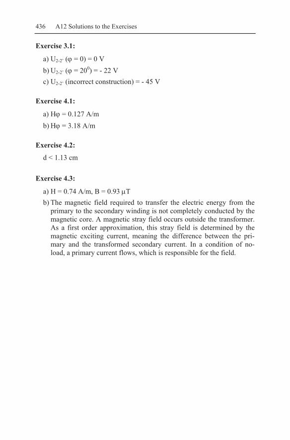
436 A12 Solutions to the Exercises
Exercise 3.1:
a) U2-2’ (ϕ = 0) = 0 V b) U2-2’ (ϕ = 200) = - 22 V c) U2-2’ (incorrect construction) = - 45 V
Exercise 4.1:
a) Hϕ = 0.127 A/m b) Hϕ = 3.18 A/m
Exercise 4.2:
d < 1.13 cm
Exercise 4.3:
a) H = 0.74 A/m, B = 0.93 μT b) The magnetic field required to transfer the electric energy from the
primary to the secondary winding is not completely conducted by the magnetic core. A magnetic stray field occurs outside the transformer. As a first order approximation, this stray field is determined by the magnetic exciting current, meaning the difference between the pri-mary and the transformed secondary current. In a condition of no-load, a primary current flows, which is responsible for the field.

A12 Solutions to the Exercises 437
Exercise 4.4:
a)
(0; 0.1; 0) 1.0; 0.1; 0)(0.5; 0.1; 0)
B[dB ]pT μT
200 10.000
180 1.000
160 100
140 10
100
80
60
0.01
0.001
twisted cable
rebuilding by cells
b) D = 10.8 dB (the twisted cable yields higher values)
Exercise 4.5:
a) Hz = - 3.18 A/m b) Hz = - 2.85 A/m c) Ampere’s law in the form of equation 4.3 requires complete symme-
try; for instance, the magnetic field of an infinitely long conductor can be calculated. With equation 4.7, there is no point where the cur-rent circuit is closed. In conclusion, the result of this equation can only form part of a more extensive calculation.
d) x = 0.141 m
Exercise 4.6:
a) B (10 m; 10 m; 7.5 m) = 360 μT b) Ui = 4.5 V c) H (0; 0.3 m; 5 m) = 13.2 kA/m
Exercise 5.1:
a) S = 2.29 mW/m b) vx = 260 km/ms c) 5.3 mA/m at h = 0, 30 m, 60 m, 90 m,...

438 A12 Solutions to the Exercises
Exercise 5.2:
a) Htan, Hnorm, Etan = 0 b) Spar = 2.49 mW/m2, Ssenk = 0.91 mW/m2
c) The parallel part will be guided undamped above the plane. The per-pendicular part will be reflected. The reflected part combines with the impinging part leading to the interference pattern.
Exercise 5.3:
a) σ(x) = Dz(x) = 220
00
22ln
)(hx
h
Rh
UxEz +⋅⋅−=⋅ εε
b) 22
)()(hx
hIxHxJ xF +⋅==
π
c) σmax = 334 pAs/m2, JF,max = 3.18 A/m
Exercise 5.4:
a) ω
0max
IQ =
b) Qmax = 0.16 µAs
Exercise 5.5: Ieff = 0.5 A
Exercise5.6:
The pointing vector is given by HES ×= . ϑϕ HwithtogetherE +− leading to a radiation direction away from the radiation source (in +r-direction).
Exercise 5.7:
a) 270 μV/m b) 42.7 μV/m
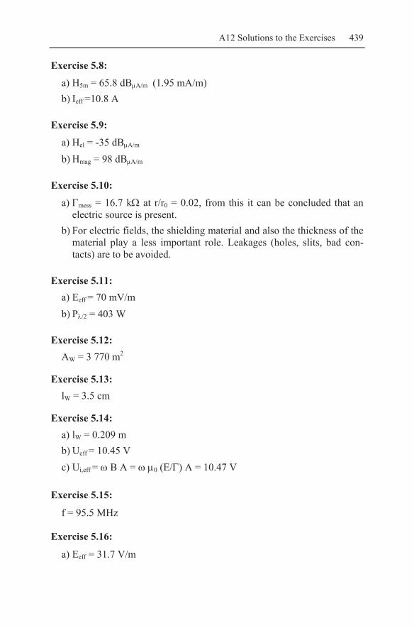
A12 Solutions to the Exercises 439
Exercise 5.8:
a) H5m = 65.8 dBμA/m (1.95 mA/m) b) Ieff =10.8 A
Exercise 5.9:
a) Hel = -35 dBμA/m b) Hmag = 98 dBμA/m
Exercise 5.10:
a) Γmess = 16.7 kΩ at r/r0 = 0.02, from this it can be concluded that an electric source is present.
b) For electric fields, the shielding material and also the thickness of the material play a less important role. Leakages (holes, slits, bad con-tacts) are to be avoided.
Exercise 5.11: a) Eeff = 70 mV/m b) Pλ/2 = 403 W
Exercise 5.12: AW = 3 770 m2
Exercise 5.13: lW = 3.5 cm
Exercise 5.14: a) lW = 0.209 m b) Ueff = 10.45 V c) Ui,eff = ω B A = ω μ0 (E/Γ) A = 10.47 V
Exercise 5.15:
f = 95.5 MHz
Exercise 5.16:
a) Eeff = 31.7 V/m
440 A12 Solutions to the Exercises
b) The wavelength of the electromagnetic radiation amounts to 306 m. The danger of exciting electromagnetic resonances is still low for ve-hicles and the cables installed in the vehicles.
Exercise 5.17:
UL,eff = 12.8 mV
Exercise 5.18:
a) Ieff = 7.55 A b) E = 9.5 mV/m, H = 25.2 μA/m c) If the radiation losses Pab are substantially higher than the losses by
conduction (thermal losses) PV (Pab >> PV), the current used for calcu-lating the radiation can also be used for calculating the conduction losses; possibly making a correction afterwards.
Calculation procedure: 1. Prediction of the current, necessary for the radiation (lossless case):
)()( 0 zhhIzI −⋅=
2. Calculation of the resistance per unit length of the antenna consid-ering the skin effect:
μκπκπ fd
RdRW
1,2
1' ==
3. Calculation of the conduction losses (thermal losses) through use of the integral
3)(
'20
0
22
'20 hRIdzzhh
RIP Wh
WV
⋅⋅=∫ ⋅−⋅
⋅=
PV = 1.88 W
d) η = 98.2 %
e) 3108.1// −⋅=≈ BabBW PPPP
Exercise 5.19:
An electrically short linear antenna has an input impedance with a very small real part (radiation resistance). The current required to radiate at a

A12 Solutions to the Exercises 441
given power becomes very high. Therefore, a very high imaginary part of the input impedance, compared with the real part, leads to the antenna voltage becoming extremely high. The distance between the capacitor plates must be calculated for the highest possible voltage and the wire of the coils for the maximum possible current.
Exercise 5.20:
E2 = 0.1 V/m
Exercise 6.1:
The resonance of a screen of a 5.3 m long cable, grounded at only one
end, occurs at l = λ/4 (l
cf s ⋅=
40
Re = 14.15 MHz).
Two aspects should be taken into consideration: 1. In the evening hours, switching actions occur that excite the λ/4-
resonance. The electronics are particularly sensitive at the corre-sponding frequency.
2. A radio amateur in the neighbourhood makes intensive connections in the 20 m band, especially during the evening hours.
Exercise 6.2:
a) 11.2 mV b) 59.3 mV c) 593 mV

442 A12 Solutions to the Exercises
Exercise 6.3:
a) Partial capacitances ======================
C 1 0 = 6.036116 pF/m
C 1 2 = 2.534546 pF/m
C 1 3 = .5223917 pF/m
C 1 4 = .4358155 pF/m
C 2 1 = 2.534546 pF/m
C 2 0 = 5.537686 pF/m
C 2 3 = .8263816 pF/m
C 2 4 = .7712098 pF/m
C 3 1 = .5223917 pF/m
C 3 2 = .8263815 pF/m
C 3 0 = 4.452631 pF/m
C 3 4 = 3.148848 pF/m
C 4 1 = .4358154 pF/m
C 4 2 = .7712097 pF/m
C 4 3 = 3.148848 pF/m
C 4 0 = 4.56957 pF/m
b) U34 = 1.3 V
Exercise 6.4:
Ueff,A = 74.4 V, Ieff,F = 3.4 mA
Exercise 6.5:
a) 0.0465 μH using the program MUTUAL, 0.0413 μH using the equa-tion for parallel conductors, equation (6.14)
b) 0.0313 μH using the program MUTUAL, 0.0249 μH using the equa-tion for parallel conductors
Exercise 6.6:
a) I2 = 16.8 mA b) fü = 239 Hz c) The reaction can be neglected:
21
262 8.21022.0)( Ω=<<Ω⋅= −eigenLZM ωω .

A12 Solutions to the Exercises 443
Exercise 6.7:
a)
⎟⎟⎠
⎞⎜⎜⎝
⎛⎟⎠⎞
⎜⎝⎛+
⎟⎟⎠
⎞⎜⎜⎝
⎛⎟⎠⎞
⎜⎝⎛+
⋅=2
2
21ln
1lnlog20
sd
sd
a
b) a = 9.8 dB
Exercise 6.8:
a) 13.5 mV/m b) PEmpf = 264 nW, Ueff,Empf = 3.65 mV
Exercise 7.1:
a) n = 4
ZZ
G
L
L L
C C1
1 2
2
b) The circuit presented is suitable for filtering (low pass filtering), if the
interference source has a small source impedance ZG and the load im-pedance ZL is high. Using the inductance L1 means that the source impedance is increased. Inclusion of the capacitor C2 means that the load is capacitively short-circuited.
Exercise 7.2:
a) h = 0.134 m b) aS = 38.6 dB c) The shield arrangement may be interpreted as electrically short.
Therefore, the simple relations for static fields can still allowed be used. The actual shielding efficiency is substantially higher because, as a resulting of an alternating field in the wire mesh, a current is pro-duced that additionally compensates the outer field to be shielded.

444 A12 Solutions to the Exercises
Exercise 7.3:
a) EMitte = 57.5 mV/m b) I = 0.42 μA c) Grounding is not necessary for the effect of shielding. However, for
personnel protection reasons (personnel protection insulation) and for leading static electricity to ground, grounding is highly recom-mended.
Exercise 7.4:
a) High magnetic alternating fields occur in the vicinity of the railroad tracks (in Germany: at 16 2/3 Hz). The starting current of the trains may be several times higher than the normal driving current. As the power feeding into the tracks occurs only selectively (at certain points), the track section with increased fields depends on the position of the starting train with respect to the feeding point.
b) The greatest possible distance (r > 50 m) for the point of installation from the conductor rail should be chosen during the planning phase (best solution),
- Changeover to a LCD-monitor (with it no further restriction with regard to the installation place),
- Compensation coils (needs external supply), - Mu-metal housing (only conditionally, because of the direction de-
pendence and the comfort restrictions, worst solution).
Exercise 7.5:
t = 0.63 mm
Exercise 7.6:
a) aS = 8.0 dB b) aS = 7.9 dB c) aS = 9.8 dB
Exercise 7.7:
μμ0,sin1
21coslog20 ⋅=⋅⋅⎟
⎠⎞
⎜⎝⎛ ++⋅⋅= kKtkh
KKtkhaSW ,

A12 Solutions to the Exercises 445
0,00,1)1( →→⇒→⋅+== Kkfd
jjk κμω
( )R
ttktkK
tkhK
Ktkh r ⋅⋅+→⎟⎟
⎠
⎞⎜⎜⎝
⎛ ⋅+⋅⋅+→⋅⋅⎟
⎠⎞
⎜⎝⎛ ++⋅
μ211
!31
211sin1
21cos
3
⎟⎠⎞
⎜⎝⎛ ⋅
⋅+⋅=R
ta rSG
μ211log20
Exercise 7.8:
a) cmDR 32.1732
=⋅
= . Regarding alternating magnetic fields, the
shielding efficiency increases with increasing size of the space to be shielded. For that reason, a ‘worst-case’-estimation has to take the in-ner-sphere as the substitute arrangement.
b) cmDR 49.2432
=⋅
= Regarding magnetic DC-fields, the shielding
decreases with increasing size of the space to be shielded. For that reason, a ‘worst-case’-estimation has to take the outer cylinder as the substitute arrangement.
Exercise 7.9:
The external field to be shielded can be decomposed into a transverse and a longitudinal field: Ha,quer = 1 A/m, Ha,längs = 1.732 A/m. A trans-verse field of 1 A/m produces an inner field of 26.1 – j 97.6 mA/m, a longitudinal field of 1 A/m produces an inner field of –104.3 –j 279.5 mA/m. Hence, the results are mAeH j
queri /101.0075
,−⋅= and
mAeH jlängsi /517.0
05.110,
−⋅= .
Exercise 7.10:
The shielding efficiency of housings made of highly permeable materi-als against magnetic DC-fields can be approximated by
⎟⎠⎞
⎜⎝⎛ ⋅
⋅⋅≈R
ta rSG
μ21log20 , t = thickness of the material, R = radius of the
substituting cylinder. Doubling the radius requires a doubling of the ma-terial thickness in order to obtain the same shielding efficiency. Using

446 A12 Solutions to the Exercises
the data of the example leads to a room shielding with Mu-metal walls of approximately 1 cm in thickness (purely theoretical).
Exercise 7.11:
fG = 1.02 1018 Hz
Exercise 7.12:
a) Hertzian dipole: j
rr
rrj
rr
WHD
+
⎥⎥⎦
⎤
⎢⎢⎣
⎡−⎟
⎠⎞
⎜⎝⎛−
⋅=0
2
00
0
1ΓΓ
Magnetic dipole:
rrj
rr
rrj
WMD
0
2
0
0
0
1
1
⋅−⎟⎠⎞
⎜⎝⎛−
⋅−⋅= ΓΓ
b) jWHD +
⋅=1
10ΓΓ
c) )1(0 jWMD +⋅= ΓΓ
Exercise 7.13:
Interpreting d⋅κ
1 as the HF-surface resistance, RF,HF, of the material
yields a wave impedance of Γm = (1+j) RF,HF. The HF-surface resistance is the resistance of a quadratic probe with the dimensions l = b (length equal to the width) and a thickness equal to the skin depth.
Exercise 7.14:
In order to be able to interpret a shielding efficiency value then, apart from the value alone, the field type, the frequency and the distance to the shielding wall must also be known. If the value to be understood is a measured value then the method of measurement should also be given.

A12 Solutions to the Exercises 447
Exercise 7.15:
a) ram = -0.9999978 + j 2.22 10-6 b) J0 = 252.5 (1+j) A/m2
Exercise 7.16:
Sniffer-Test: This test is carried out far below the critical frequency of the rebuilding waveguide of the channel (fg = 375 MHz). Therefore it is carried out in a frequency range in which no wave propagation within the channel is possible. As a result, an insulated cable should be led into the channel, which is excited at one end, against the channel, by a HF-signal of 200 .... 500 kHz and terminated at the far end by approxi-mately 100 ... 150 Ω against the channel. The outer region of the chan-nel has to be checked for leakages using a receiving coil. Leakage-Test: The test should be carried out above 375 MHz. Through use of a suitable antenna, the empty channel is excited as a waveguide above its critical frequency. The outer region of the channel has to be checked for leakages using a receiving antenna.
Exercise 7.17:
a) aS = 39.8 dB b) aS = 186.9 dB c) The transformation of a meshed shield into a foil shield is not allowed
for a static field. The shielding efficiency becomes infinitively high. In deriving the equations it is assumed: - The E-field lines end perpendicular to the meshing wires for
meshed shields. - In Schelkunoff’s theory, a plane wave (E-field lines parallel to the
wall) is impinging onto the wall. - No induction processes are considered with meshed shields.
Exercise 7.18:
Ltube = 11.25 cm (pure waveguide attenuation)
Exercise 7.19:
f110 = 53 MHz, f101 = f011 = 62.5 MHz, f111 = 72.9 MHz, f210 = 83.8 MHz, f201 = 90.1 MHz

448 A12 Solutions to the Exercises
Exercise 7.20:
a) aS = 96 dB b) aSges = 180 dB c) The length may be shortened by 44 % , L = 0.56 Lalt.
Exercise 7.21:
a) fr = 4.57 kHz b) aSA = 27.3 dB
Exercise 7.22:
Ui = 0.19 μV
Exercise 7.23:
a) UOP = 0.2 V
b) dBdBU
U
mmmm 1.0log20
52.2 =⋅
c) Adding an additional shielding to the twisted cable, with a connection of the shield at both ends to ground, results in a significant reduction in the voltage coupling into the signal circuit.
Exercise 7.24:
fG = 1.04 kHz
Exercise 7.25:
a) AlR
UI Hz μ947'2
2100,1 =
⋅≈
b) mAlL
UI MHz 25.8'2
21,2 =
⋅≈
ω
Exercise 7.26:
UA = 428 μV

A12 Solutions to the Exercises 449
Exercise 7.27:
H(h2) = 112.8 mA/m
Exercise 8.1:
S/Ngesamt = 7.2 dB
Exercise 8.2:
a) S/NEmpf = 22 dB b) S/NSonne = 6.7 dB c) Undisturbed reception in not possible, S/Nges = 6.6 dB.
Exercise 8.3:
a) En = 10.5 dBμV/m
b) VEUG
nLeerl μπλ
λ
7.6210 202/
=⋅⋅=
Exercise 8.4:
a) f = 30 MHz → λ = 10 m → r0 = 1.6 m, the test object is small com-
pared with the wavelength: mVNM
MN dBrrEE /5.49 μ=⋅=
b) f = 100 MHz → λ = 3 m → r0 = 0.48 m, the test object with its power supply and sensor cable act as a linear
antenna: mVNM
MN dBrrEE /5.39 μ=⋅=
c) Assuming the diagonal of the radiating surface of a 19“-plug-in hous-ing to be D = 0.7 m, it is calculated that the Fraunhofer zone starts at a value of rF = 3.26 m. Therefore, an electric field strength calculation
is justifiable, yielding mVNM
MN dBrrEE /5.29 μ=⋅= .
Exercise 8.5:
EV = -24 dBμV/m
450 A12 Solutions to the Exercises
Exercise 8.6:
a) H0 = 42 dBμA/m b) EV0 = 93.5 dBμV/m c) H0 = -69 dBμA/m, EV0 = -17.5 dBμV/m
Exercise 10.1: The statement is considered to be almost impossible. To produce a field strength of 10 V/m at a distance of 10 m from a radiated power of 5 W would require an antenna gain of Gi = 18.3 dB is necessary.
Exercise 10.2:
Eeff,max = 7.2 V/m
Exercise 10.3: Cstat = 95.3 pF
Exercise 10.4:
Lself = 0.81 μH
Exercise 10.5:
a) CONCEPT: L1 = 3.32 μH, L2 = 4.96 μH, M12 = 0.264 μH b) MUTUAL: L1 = 3.27 μH, L2 = 4.90 μH, M12 = 0.262 μH c) I2,CONCEPT= 0.256 A, I2,MUTUAL= 0.260 A, the difference is smaller than
1 dB
Exercise 10.6:
a) Z21 = - 0.708 + j 19.148 kΩ, Z12 = - 0.402 + j 19.186 kΩ The open circuit at the antenna input has been simulated by a load im-pedance of 100 MΩ. The agreement can be considered to be very good, taking into account the extreme situation of the capacitive cou-pling of two electrically short antennas.
b) Z21 = - 0.26 + j 18.53 Ω, Z12 = - 0.23 + j 18.54 kΩ The open circuit at the antenna inputs has been simulated using a load impedance of 1 MΩ. The matching is very good.

A12 Solutions to the Exercises 451
c) Z21 = - 0.021 + j 0.108 Ω, Z12 = - 0.021 + j 0.108 kΩ The open circuit at the antenna inputs has been simulated using a load impedance of 1 MΩ. The matching is perfect.
Exercise 10.7:
a) he = hMast – λ/4 = 13.5 m b) hm = hMast = 16 m oder hm = hMast –λ/2 = 13.5 m c1) he = hMast – λ/4 = 12.25 m c2) hm = hMast = 16 m oder hm = hMast – λ/2 = 8.5 m
d)
0.02
0.10
0.12
0.06
0.08
0.04
I(z)[A]
z [m] 2 4 6 8 10 12 14 16 z = h
e) E(z = 15.9 m) = 58 V/m, H(z = 15.9 m) = 15 mA/m, E(z = 13.5 m) = 18 V/m, H(z = 13.5 m) = 93 mA/m
Exercise 10.8:
a) A cable connected to ground at both ends experiences a first reso-
nance at MHzl
cf beids 75.182
0,Re =
⋅= .
b) A cable connected to ground at only one end experiences a first reso-
nance at MHzl
cf eins 375.94
0,Re =
⋅= .
Exercise 10.9:
a) 1 MHz: Z11 = 0.5810 – j1256 Ω, Z22 = 1.061 – j1097 Ω, Z12 = 0.8192 – j33.74 Ω, Z21 = -0.8130 – j33.76 Ω
3 MHz: Z11 = 5.866 – j 338.8 Ω, Z22 = 11.48 – j 234.5 Ω, Z12 = -7.573 + j6.568 Ω, Z21 = -7.571 + j6.589 Ω
8 MHz: Z11 = 88.52 + j 205.3 Ω, Z22 = 789.3 + j 690.2 Ω, Z12 = -24.01 + j 183.7 Ω, Z21 = -24.12 + j 183.2 Ω

452 A12 Solutions to the Exercises
b) 1 MHz: P2 = 0.97 P1 (97 %), 3 MHz: P2 = 0.54 P1 (54 %), 8 MHz: P2 = 0.10 P1 (10 %)
c) The coupling becomes smaller with increasing frequency. At f = 1 MHz (r0 = 47.75 m) and f = 3 MHz (r0 = 15.9 m), antenna 2 is located in the electric near-field of antenna 1 (with decreasing field impedance from 1 MHz to 3 MHz). At f = 8 MHz (r0 = 5.96 m) an-tenna 2 is still located in the near-field of antenna 1 (D < l1 < l2), but the nature of the field is no longer non-ambiguous.
Exercise 10.10:
a) ZA,2 = 54.88 + j 123.5 Ω,
b) ZA,1 = 50 Ω, Pab = 100 W c) Pab = 41.8 W
Exercise 10.11: a)
2 4 6 8 10
-330
-332
-334
-336
-338
j 225
j 220
j 210
j 232
j 250
Re ( ) [ ]
ZΩ
Im ( ) [ ]
ZΩ
11
11
Remark: The parameter values inside the circle refer to the load val-ues of antenna 2 given in Ohms.
b) The locus of the input impedance of antenna 1, for the imaginary axis of the load impedance plane, is a circle. This results in the circle sur-rounding all possible values of the input impedance of antenna 1. A matching network for antenna 1 must be able to match all values in-side the circle to the output impedance of the transmitter.
Exercise 10.12:
With help of a coil of L = 0.381 μH positioned at the half the height, a purely real antenna input impedance is achieved.

A12 Solutions to the Exercises 453
Exercise 11.1:
The fault frequency can be calculated to be h = 0. Using Eq. 11.18 and a statistical confidence of ß = 0,95, the upper confidence limit can be calcu-lated to be po = 0.3. The resulting probability of a susceptibility fault is within the interval [0;0.3]. This means, therefore, that if the equipment is tested again, malfunction could be registered in 30% of all cases.

A13 Physical Constants and Conversion Relations
A13.1 Physical Units and Constants
Absolute temperature CK °−= 15.273 Angström mA 1010−=
Boltzmann-Constant KJ231038047.1 −=κ
Density of air 31.2929airkgm
ρ =
Dielectric constant of free space VmAs12
0 10854.8 −=ε
Dielectric strength of air for a ho-mogeneous field cm
kVED 30=
Radius of an electron mre15104.1 −=
Energy of an electron accelerated by 1 Volt JeV 19106030.1 −=
Elementary charge Ase 1910603.1 −−= Faraday-Constant (for monovalent materials) mol
CF 96487=
Density 38.96Cu
gm
ρ =
Concentration of electrons 2838.45 10n
nn
m=
Mobility of electrons 2
443 10n
mVs
μ −=
Conductivity 657 10Cu
Sm
κ =
Copper
Fusion point 1083.4fusionT C= °
K.-H. Gonschorek, R. Vick, Electromagnetic Compatibility for Device Design and System Integration, DOI 10.1007/978-3-642-03290-5_24, © Springer-Verlag Berlin Heidelberg 2009

456 A13 Physical Constants and conversion relations
Velocity of light in vacuum smc 6
0 108.299=
Mass of the earth kgmE2410977.5=
Acceleration of mass on earth due to gravitation 281.9
s
mg =
Permeability constant of free space AmVs6
0 104.0 −= πμ
Planck constant Jsh 3410624.6 −=
Radius of the earth, equator kmrE 6378=
Radius of the earth, pole kmrp 6356=
Rest mass of an electron kgme31101066.9 −=
Rest mass of a neutron kgmn27106749.1 −=
Rest mass of a proton kgm p271067248.1 −=
Triple point of water 273.16waterT K=
Universal gravitational constant 2
21110658.6
kgs
mG −=
Ideal gas constant 423144.8
Km
WR =
Impedance of free space Ω=Γ 6.3760
Standard pressure 25
0 10101325.1mNp =
A13.2 Conversion table for pressure
Bar at Torr 2m
N 2m
kp atm
bar 1.020 750.1 105 1.0197⋅104 0.9869 at 0.9807 735.6 0.9807⋅105 104 0.9678
Torr 1.333⋅10-3 1.360⋅10-3 133.3 13.60 1.3158⋅10-3 2/ mN 10-5 1.020⋅10-5 0.7501⋅10-2 0.1020 0.9869⋅10-5
2mkp 0.9807⋅10-4 10-4 0.7356⋅10-1 9.807 0.9678⋅10-4
atm 1.0132 1.0332 760 1.0132⋅105 1.0332⋅104

A13 Conversion table for energy 457
A13.3 Conversion table for energy
J kcal kpm 1 kWh 1 PS h J= Ws= Nm
2.389⋅10-4 0.1020 2.778⋅10-7 3.777⋅10-7
kcal 4.187⋅103 427.0 1.163⋅10-3 1.581⋅10-3 kpm 9.807 2.342⋅10-3 2.724⋅10-6 3.704⋅10-6 kWh 3.6⋅106 859.8 3.671⋅105 1.360 PS h 2.648⋅106 632.4 2.7⋅105 0.7355
Example for using the table: 1 J = 2.389 10-4 kcal
A13.4 Conversion relations for electric and magnetic quantities
Electric resistance 1 Ohm 23
12
1/11AskgmAV ==Ω
Electric power 1 Watt 3
12
111skgmVAW ==
Electric energy 1 Joule 2
12
1111skgmVAsWsJ ===
Capacitance 1 Farad 12
24
1/11kgmAsVAsF ==
Electric field strength 1 Volt per Meter mV /1
Dielectric flux density As
kgmAs2
12 1/1 =
Inductance 1 Henry 22
12
1/11AskgmAVsH ==
Magnetic field strength 1 Ampere per Meter
mA /1
1 Tesla 12
1
221111
Askg
mWb
mVsT ===
TTG μ100101 4 == − Magnetic flux density 1 Gauß
0/6.791 μμ == fürmAG
Magnetic flux 1 Weber 12
12
11AskgmVs =

458 A13 Physical Constants and conversion relations
Voltage, potential 1 Volt 13
12
11AskgmV =
A13.5 Conversion of logarithmic quantities
• 1 Neper = 8.686 dB⇔ 1 dB = 0.1151 Neper • 0 dBm = 107 dBµV für Ri = 50 Ω (1 mW corresponds to 0.2236 V
across 50 Ω) • 0 dBm = 117.8 dBµV für Ri = 600 Ω (1m W corresponds to 0.7746 V
across 600 Ω)
Table A13.1 Some relations for calculations with dB-values
Factor dB- value for power or for engergy
dB- value for current, voltage and related field values
1 0 0 2 3 6 3 5 (4.8) 10 (9.5) 10 10 20 100 20 40 1000 30 60 1/2 -3 -6 1/3 -5 (-4.8) -10 (-9.5) 0.1 -10 -20 1.1 (+10%) 0.5 (0.414) 1 (0.828) 0.9 (-10%) -0.5 (-0.414) -1 (-0.915) 1.01 (+1%) 0.05 (0.0432) 0.1 (0.0846) 0.99 (-1%) -0.05 (-0.0436) -0.1 (-0.0872)
Examples for using the table:
6872 V = (2⋅2⋅2⋅2⋅2⋅2⋅100 + 8 %) V ⇔ (6+6+6+6+6+6+40+0.8) dBV = 76.8 dBV (76.74 dBV) 375 mA = (1/2/2/2⋅3) A ⇔ (0-6-6-6+9,5) dBA = -8.5 dBA (-8.52 dBA)
54 dBµV/m = (20+20+20-6) dBµV/m ⇔ (10⋅10⋅10/2) µV/m = 500 µV/m

A13 Abbreviations 459
A13.6 Abbreviations
ANSI American National Standards Institute BCI Bulk current injection BEM Boundary element method BSI British Standards Institution CDN Coupling-decoupling network
CENELEC European Committee for Electrotechnical Standardi-zation
CISPR Int. Special Committee on Radio Interference COTS Commercial off the shelf
DKE Deutsche Kommission Elektrotechnik Elektronik In-formatik (German commission for electrotechnique)
EEG Electro encephalogram
EIRP Equivalent isotropically radiated power
EKG Electro cardiogram
ELF Extremely low frequency
EMC Electromagnetic compatibility
EMG Elektro myogram
EMI Electromagnetic interference ERP Effective radiated power, 1.64*ERP = EIRP ESD Electrostatic discharge
EUT Equipment under test
ETSI European Telecommunication Standards Institute
FCC Federal Communications Commission
FDTD Finite differences time domain
GRP Ground reference plane
GTD Geometrical Theory of Diffraction

460 A13 Physical Constants and conversion relations
GTEM Gigahertz Transverse Electromagnetic
HIRF High Intensity Radiated Field
HPM High power microwaves
IEC Internationale elektrotechnische Kommission (Inter-national Electrotechnical Commission
ISM Industrial, Scientific and Medical ISO International Organization for Standardization ITU International Telecommunication Union LCL Longitudinal Conversion Loss LEMP Lightning Electromagnetic Pulse LISN Line impedance stabilization network MIL-STD Military standard MOM Method of Moments NEMP Nuclear electromagnetic pulse NIST National Institute of Standards and Technology NSA Normalized Site Attenuation PLC Power line communication RADHAZ Radiation hazards SAR Specific Absorption Rate SHF Super high frequency SMD Surface mounted device
STANAG Standardization Agreement
SWR Standing wave ratio
TEM Transverse Electromagnetic Mode
THD Total Harmonic Distortion
TLM Transmission Line Model
TREE Transient Radiation Effects on Electronics
TTE Telecommunication Terminal Equipment

A14 Bibliography
[AD/ME73]
Adams, A.T., Mendelovicz, E.: „The Near-Fild Polari-zation Ellipse“, Trans. IEEE AP 1973, pp 124–126
[AN91] ANSI C63.16-1991 (Draft) 1991 Guide for Electro-static Discharge Test Methodologies and Criteria for Electrostatic Equipment
[BI/HA59] Bickmore, R.W., Hansen, R.C.: „Antenna Power Den-sities in the Fresnel Region“, Proc. IRE, Dec. 1959, pp. 2119–2120
[BOE02] Böge, W.: „Vieweg Handbuch Elektrotechnik 2. Au-flage“, vieweg, Braunschweig/Wiesbaden, 2002
[BU/GO97] Buss, E., Gonschorek, K.H.: “EMV der aktuellen Ma-rine-Projekte F124 und U212”, Wehrtechnisches Sym-posium Elektromagnetische Verträglichkeit EMV 97, Mannheim 1997
[Bu87] Bush DR (1987) Statistical Considerations of Electro-static Discharge Evalua-tions. 1987 Zurich Interna-tional Symposium on EMC: 487-490
[CH/SI80] Chari, M.V.K., Silvester, P.P.: “Finite Elements in Electrical and Magnetic Field Problems”, J. Wiley, Toronto, 1980
[CIS92] CISPR publication 16: “CISPR Specifications for Ra-dio Interference Measuring Apparatus and Measure-ment Methods”
[FAR03] Faria, B.: „The Polarization Ellipsoid Revisited“, EMC, IEEE EMC Society Newsletter, No. 198, 2003, pp. 38–39
K.-H. Gonschorek, R. Vick, Electromagnetic Compatibility for Device Design and System Integration, DOI 10.1007/978-3-642-03290-5_25, © Springer-Verlag Berlin Heidelberg 2009

462 A14 Bibliography
[GON80] Gonschorek, K.H.: “Die Berechnung des elektromag-netischen Impulsverhaltens dreidimensionaler Anord-nungen schlanker Elektroden“, PhD Thesis Hochschu-le der Bundeswehr, Hamburg, 1980
[GON82] Gonschorek, K.H.: “Numerische Berechnung der durch Steilstromimpulse induzierten Spannungen und Ströme“, Siemens Forsch.- und Entwickl.-Ber. Bd 11 (1982) Nr. 5, Seiten 235–240
[GON84] Gonschorek, K.H.: “Elektromagnetische Verträglich-keit (EMV) in Systemen mit eng benachbarten Anten-nen“, FREQUENZ 38 (1984) 4, Pages 78–84
[GON85] Gonschorek, K.H.: "Magnetic Stray Fields of Twisted Multicore Cables and Their Coupling to Twisted and Non-Twisted Two-Wire Lines", 6. Int. Symposium on EMC, Zurich 1985, Paper 96 P 7
[GO/NE93] Gonschorek, K.H., Neu, H.: “Die elektromagnetische Umwelt des Kraftfahrzeuges”, FAT Schriftenreihe Nr. 101, Forschungsvereinigung Automobiltechnik EV, Frankfurt/Main, 1993
[GON88] Gonschorek, K.H.: „Beeinflussung von Rechnerkom-ponenten durch niederfrequente Magnetfelder“, Kon-gress EMV ’88, Scientific contributions, Pages 91–101
[GO/SI92] Gonschorek, K.H., Singer, H.: „Elektromagnetische Verträglichkeit“, B.G. Teubner, Stuttgart 1992
[Ha92] Habiger E, u. a. (1992) Elektromagnetische Verträg-lichkeit - Grundlagen Maßnahmen und Systemgestal-tung. Verlag Technik, Berlin
[Ha/Wo/We94] Was leisten normgerechte EMV-Störfestigkeits-nachweise gegenüber pulsförmigen Prüfstörgrößen aus statistischer Sicht?. In: Schmeer HR (Hrsg) Elektro-magnetische Verträglichkeit / EMV'94, Int. Fachmesse und Kongress für Elektromagnetische Verträglichkeit. vde-verlag, Berlin
A14 Bibliography 463
[HE/HA/GON99] Helmers, S., Harms, H.-F., Gonschorek, K.H.: Analyz-ing Electromagnetic Pulse Coupling by Combining TLT, MoM , and GTD/UTD”, IEEE TEMC, Nov. 1999
[ITU64] C.C.I.R.-Report 322, „World distribution and charac-teristics of atmospheric radio noise“, ITU Genf, 1964
[KAD59] Kaden, H.: „Wirbelströme und Schirmung in der Nachrichtentechnik“, Springer-Verlag, Berlin, 1959
[Le/Mo04] Verkopplung der Innenräume von Gehäusen mit Öff-nungen über externe Verkabelung, Beitrag zum EMV-Kongress 2004, Düsseldorf
[ME/GU] Meinke, H., Gundlach, F.W.: „Taschenbuch der Hoch-frequenztechnik“, Springer-Verlag, Berlin 1968
[Me78] Shielding theory of enclosures with apertures, IEEE TEMC, Vol. 20, No. 2, PP. 296-305, May 1978
[MO/KO80] Mönich, G., Kombrink, F.: „Simultanbetrieb zweier Sendeanlagen bei eng benachbarten, abgestimmten Antennen“, Frequenz 34 (1980) 6, Seiten 158–164
[NC/PI/MA90] McNamara, D.A., Pistorius, C.W.I., Malherbe, J.A.G.: „The Uniform Geometrical Theory of Diffraction“, Artech House, Boston, 1990
[Ni/Os90] Diagnostic Effectiveness in Computer Systems Using Deterministic Random ESD. 1990 IEEE International Symposium on Electromagnetic Compatibility: 274-279
[Re92] Optimized Statistical Method for System-Level ESD Tests. 1992 IEEE International Symposium on Elec-tromagnetic Compatibility: 474-484
[SCH94] Schlagenhaufer, Fr.: „Berechnung transienter Ver-gänge auf verlustbehafteten Leitungen mit Feldan-regung“, Diss. TU Hamburg-Harburg, 1994
[SC/HE/FY03] Schlagenhaufer, F., He, J., Fynn, K.: „Using N-Port-Models for the Analysis of Radiation Structures“, Sci. Cont. to IEEE Symp. On EMC, Istanbul, 2003
[SIN69] Singer, H.: „Das Hochspannungsfeld von Gitterelek-

464 A14 Bibliography
troden“, PHD Thesis TU München, 1969
[SI/ST/WE74] Singer, H., Steinbigler, H., Weiss, P.: „ A Charge Simulation Method for the Calculation of High Volt-age Fields“, Trans. IEEE, PAS-93, 1974
[TI/GO98] Tiedemann, R., Gonschorek, K.H.: „Einfaches Ver-fahren zur Bestimmung der komplexen Kabeltransfer-impedanz“, Teil1: EMV-ESD, 2/98, Seiten 28–31 Teil2: EMV-ESD, 3/98, Seiten 27–29
[TIE01] Tiedemann, R.: „Schirmwirkung koaxialer Geflechtss-trukturen“, PhD Thesis TU Dresden, 2001
[VAC88] Firmenschrift FS-M 9 der Fa. Vacuumschmelze GmbH, Hanau, 1988
[VAN78] Vance, E.F.: „Coupling to Shielded Cables”, John Wiley & Sons, New York,1978
[VG993] Beiblatt 1 zu VG 95 374 Teil 4: „Elektromagnetische Verträglichkeit (EMV) einschließlich Schutz gegen den Elektromagnetischen Impuls (EMP) und Blitz, Programm und Verfahren, Verfahren für Systeme und Geräte, Rechenverfahren für die EMV-Analyse“, Beuth Verlag, Berlin, 1993
[VG994] VG 95375-3: „Grundlagen und Maßnahmen für die Entwicklung von Systemen, Teil 3: Verkabelung“, Beuth Verlag, Berlin, 1994
[VG996] Beiblatt 2 zu VG 95374-4: „Elektromagnetische Ver-träglichkeit (EMV) einschließlich Schutz gegen den Elektromagnetischen Impuls (EMP) und Blitz, Pro-gramm und Verfahren, Teil 4:Verfahren für Systeme und Geräte, EMV-Analyse von Kabelkopplungen“, Beuth Verlag, Berlin, 1996
[Vi95] Die Abhängigkeit der Störfestigkeit digitaler Geräte von den internen Funktionsabläufen. PhD Thesis; Technische Universität Dresden

A14 Bibliography 465
[We96] Störfestigkeit computerbasierter Geräte gegenüber pulsförmigen elektrischen Störgrößen - Statistische Modellierung und Störfestigkeitsprüfung mit sta-tistischen und selbstadaptiven Methoden. PhD Thesis Technische Universität Dresden

Index
A
abbreviations ..............................459 absolute temperature...................455 acceleration of mass on earth......456 antenna coupling.........................275 antenna gain Gk ............................69 aperture antennas..........................75 application examples of analysis 265 atmospheric noise ...............205, 208
B
Babinat’s principle .....................167 band pass ....................................132 Binomial distribution..................292 Boltzmann-Constant ...................455 burst............................................205 Butterworth-low pass .................137
C
cable categories ..................127, 398 cable coupling.............................171 cable shield connection...............200 cable transfer impedance ....171, 409 cable trays...................................399 cabling ................................122, 123 capacitances................................421 capacitive coupling.......................93 cavity resonances........................157 charge density...............................19 circuit analysis............................253 circular polarization....................369 closed line integral........................20 compensation coils .....................145 concentric cylinders....................422 concentric spheres ......................421 conceptual phase.........................227 conducting half space .................377 conductor between 2 planes........425 conductor loops in space ............341 construction and building phase .230 conversion E H ......................221
conversion H E ......................222 conversion of limit values ..........218 conversion table for energy ........457 conversion table for pressure......456 core radius ..................................173 coupling................................97, 104 coupling out................................191 critical state.................................299 current.............................................9 current density ..............................19 cylindrical conductor / plane ......423
D
definition phase ..........................228 density of air ...............................455 development phases....................227 dielectric strength of air..............455 directivity......................................69 directivity functions....................186 displacement current density ........19 distance conversion ..............61, 218 double-walled shields .................144
E
earthing.......................................393 eccentric cylinders ......................423 effective antenna area .............68, 70 effective height .............................68 effective mutual inductance........101 effects of electric fields ................22 effects of electromagnetic fields...50 effects of magnetic fields..............29 effektive antenna height .........70, 74 EIRP ...........................................109 electric charge...............................19 electric field strength ................8, 22 electrically thick materials..........385 electrically thin materials ...........385 electromagnetic coupling............106 electromagnetic environment ....205,
214 electromagnetic field ....................19 electromagnetic waves..................45
K.-H. Gonschorek, R. Vick, Electromagnetic Compatibility for Device Design and System Integration, DOI 10.1007/978-3-642-03290-5_BM2, © Springer-Verlag Berlin Heidelberg 2009

468 Index
electrostatic discharge ..................87 elementary dipoles......................347 elliptical cable ............................422 EMC design guide......................393 EMC engineering .......................225 EMC- test planning ....................232 EMC-design guide......................123 EMC-design-pyramid.................401 EMC-forecast .............................227 EMC-plan...................................227 EMC-system test ........................231 EMC-zones.................................226 emission limit .............................213 ESD ............................................205 execution of analysis ..................242
F
far field region..............................76 Faraday-Constant .......................455 fault frequency............................290 fault frequency function .............292 field impedance ......................57, 66 field of a single layered coil .......329 field strength in main beam
direction ...................................71 filtering...............................122, 129 finite differences.................254, 255 finite elements ............................254 five-step-procedure.....................242 flowchart for cable coupling.......128 Fourier transform........................176 Fraunhofer region.........................75 Fresnel region...............................75
G
galvanic coupling .........................90 galvanic decoupling......................92 Geofol transformer .......................34 grounding ................... 122, 123, 393
H
Hertzian dipole .....................54, 347 HF...............................................417 high frequency field .....................21
high impedance field ....................58 high pass.....................................132 HLEITER ...................................309 hollow cylinder...........................151 horizontal polarization..........48, 186 horizontally polarized wave .......183
I
immunity ....................................285 immunity testing.........................285 impedance.....................................10 impedance of free space .............456 inductive coupling ........................97 insertion loss...............................133 integral equation method ............255 interference detection ...................89 interference model........................83 interference safety margins.........240 interference source .......................85 interference victim........................85 intrasystem measures..................121
L
law of induction............................19 layered dielectric ........................421 leakage-test.................................158 limit curves.................................213 limiting the coupling impedances.92 longitudinal voltage....................188 low frequency resonances ..........167 low impedance field .....................58 low pass......................................132 low pass filter .............................133 low stray field arrangements ........33
M
magnetic decoupling...................100 magnetic dipole ............................56 magnetic field strength .................19 magnetic fields .............................29 magnetic flux................................19 magnetic flux density ...................19 magnetic stray fields.............35, 321 malfunction probability ......289, 290

Index 469
man made noise ..........................213 Maxwell’s equations...............19, 20 measures to reduce the
electromagnetic coupling .......107 medium voltage transformers .......34 mesh shields ...............................159 mirror image .................................52 multicore cables............................31 mutual inductance.......................105
N
network analyzer ........................415 N-port theory ..............................275 numerical techniques ..................247
O
operator.......................................286 oscilloscope ................................413
P
parallel cylindrical conductors....424 partial capacitances.....................308 permeability constant..................456 physical constants.......................455 pig-tail connection......................202 Planck constant...........................456 plane / plane................................421 plate with holes...........................161 plausibility check........................256 potential coefficients ..................308 power balance.............................256 probability ..................................290
Q
quasi stationary fields ...................21
R
radar equation ...............................72 radiation resistance .......71, 351, 358 radius of an electron ...................455 reciprocity...................................257 rest mass of a neutron .................456 rest mass of an electron ..............456
RG 174 .......................................418 RG 213 ...............................412, 416 RG 214 .......................................418 RG 217 .......................................419 RG 58 .........................................413 rod arrangements ........................307
S
safety ..........................................285 Schelkunoff ........................153, 377 self and mutual inductances........337 separation distances ....................128 service openings .........................143 SFELD................................320, 335 SHIELD......................................156 shielding .............................122, 138 shielding against electric fields...138 shielding against magnetic fields141 shielding efficiency ....................384 shielding efficiency for copper ...155 shielding mechanism ..................382 shielding solution .......................126 single conductor arrangement.....309 single core cables..........................31 skin effect ...................................379 sniffer-method ............................158 sphere / plane..............................422 sphere / sphere – sphere spark gap
...............................................422 standing waves ...........................168 star-four-arrangement ...................96 static fields....................................21 static magnetic fields ..................141 static stochastic system...............289 stationary fields ............................21 stochastic interpretation..............285 stray field....................................254 strong skin effect ........................379 sum vector ..................................368 susceptibility...............................289 susceptibility window.................297 switch on/switch off tests ...........235 system analysis ...........................228 system cabling ............................126
470 Index
T
three-phase cable ........................426 three-step-procedure.....................84 three-wire arrangements .............317 time invariant susceptibility .......289 time variant immunity ................296 transition distance.........................59 transmission line theory .....179, 252 triple point of water ....................456 turn length ....................................37 turn width .....................................37 twisted cable.................................38 two conductor cable ...................324 two cylindrical conductors above
ground ....................................425 two parallel conductors on a
substrate .................................427 two parallel plates.......................149 two parallel strip lines ................423 two parallel wires .......................424
two port parameter......................276
U
unsymmetrical disturbance voltages.................................................88
V
vertical antenna ..........................424 vertical conductors .....................315 vertical polarization..............49, 186 vertically polarized wave............183 voltage ............................................8
W
waveguide attenuation................162 weak skin effect..........................380
Λ
λ/2-coupling model.....................108