Embed Size (px)
Citation preview

UNIVERSIDAD DE CHILE FACULTAD DE CIENCIAS FÍSICAS Y MATEMÁTICAS
DEPARTAMENTO DE INGENIERÍA ELÉCTRICA
ELECTROMAGNETIC AND DEVICE
SIMULATIONS FOR IMPROVEMENTS ON
VERTICALLY ILLUMINATED TRAVELLING-
WAVE UNI-TRAVELLING-CARRIER
PHOTODIODES
TESIS PARA OPTAR AL GRADO DE DOCTOR EN INGENIERÍA ELÉCTRICA
VICTOR HUGO CALLE GIL
PROFESOR GUÍA
ERNEST ALEXANDER MICHAEL
PROFESOR GUÍA 2 PATRICIO MENA MENA
MIEMBROS DE LA COMISIÓN ENRIQUE MORENO PÉREZ
ANTONIO JESÚS GARCÍA LOUREIRO RICARDO FINGER CAMUS
ESTA TESIS DE INVESTIGACIÓN FUE FINANCIADA POR LA COMISIÓN
NACIONAL DE INVESTIGACIÓN CIENTÍFICA Y TECNOLÓGICA CONICYT
SANTIAGO DE CHILE 2016

i
Resumen
Los fotomezcladores Verticalmente Iluminados (VI) de Onda Viajera (TW)
de Portadores Unipolares (UTC) son fuentes continuas de radiación de THz.
Este dispositivo usa la conversión heterodino para generar señales de onda
milimétrica. Este dispositivo genera además una corriente distribuida para
incrementar su capacidad de manejar mayores cantidades de corriente y
además eliminar la limitación de constante RC.
Este trabajo se divide en simulaciones electromagnéticas de alta
frecuencia y simulaciones de dispositivos semiconductores. Los estudios de
dispositivos semiconductores se enfocan en el modelado numérico del
fenómeno de transporte de portadres proveyendo una descripción cualitativa
y cuantitativa del transporte de portadores en fotodiodos UTC. Como resultado
del análisis de semiconductor, resultados de brecha de energía, espacio de
carga, densidad electrónica, velocidad del electrón, todos ellos bajos diferentes
valores de potencia de iluminación son presentados en esta sección. Una curva
de responsividad versus potencia óptica se muestra también. Esta tesis
desarrolla además simulaciones electromagnéticas de alta frecuencia para
estudiar la propagación de la onda electromagnética a lo largo del dispositivo
VI-TW-UTC. Los fotodiodos VI-TW-UTC ultra-rápidos requieren una capa base
altamente dopada que hace de conexión conductora entre el fondo de la
estructura mesa y los contactos metálicos de la capa base. Tal estructura se
denomina mesa vertical p-i-n o de Uni-Portador. La capa base dopada tiene
una fuerte influencia en las perdidas de THz. Por lo tanto, simulaciones
electromagnéticas de alta frecuencia fueron ejecutadas en HFSS y CST
Microwave Studio para estudiar las pérdidas de THz. El dispositivo VI-TW-UTC
fue modelado como una línea de transmisión cuasi-coplanar (Q-CPW).
Posteriormente, las pérdidas de THz fueron calculadas indirectamente a través
de los parámetros de dispersión S21. Las simulaciones muestran un valle de
baja pérdida cerca de la conductividad 5 × 10⁴ Sm-1, en medio de un rango de
conductividad de excesiva absorción de THz haciendo este valor la mejor
elección para el rango de frecuencia de 0 a 2000 GHz.
Adicionalmente, estructuras de Mushroom-CPW y Wall-CPW se
desarrollaron y simularon en la presente tesis para comparar sus pérdidas de
THz. Un modelo analítico describiendo la potencia entregada a la entrada de
antena del fotomezclador se desarrolló. El modelo analítico tiene como
variables de entrada la curva de responsividad versus potencia óptica y la
absorción de THz. Como resultado, la conductividad de la capa base muy alta
es necesaria para alcanzar una potencia de THz razonablemente alta.

ii
Abstract
The Vertically-Illuminated (VI) Traveling-Wave (TW) Uni-Traveling Carrier
(UTC) photomixers are continuous sources of THz radiation. This device uses
the heterodyne conversion to generate millimeter-wave signals. This device
also generates a distributed current to increase the capability to drive higher
currents and also suppress the RC limitation. This device is also vertically
illuminated because this way of illumination allows controlling the matching
between the optical interference and the THz current traveling along the
transmission line. The incident angle between the two lasers illuminating the
photomixer controls the phase matching between the optical interference and
the THz current.
This work is focused in the numerical modeling of VI-TW-UTC photomixers
by dividing the work in semiconductor and High-Frequency RF simulations. The
semiconductor studies are focused in the numerical modeling of carrier-
transport phenomena providing quantitative and qualitative description of
semiconductor transport in UTC photodiodes. The semiconductor analysis is
based on the Hydrodynamic Carrier transport Model which treats the
propagation of electrons and/or holes in a semiconductor device as the flow of
a charged compressible fluid. As a result of the semiconductor analysis, studies
of energy bandgap, space charge, electron density, electron velocity, versus
distance, and with different applied optical powers are presented in this
section. A curve of Responsivity versus Optical power is obtained.
This thesis also performs High-Frequency RF Simulations to study the
electromagnetic wave propagation of the VI-TW-UTC device. The VI-TW UTC
ultra-fast photodiodes require a highly doped base layer that makes a well-
conducting transverse connection between the mesa bottom layer and the
bottom metal contacts. Such structure is a vertical p-i-n or uni-traveling (UTC)
mesa. The base layer doping has a strong influence in the THz losses.
Therefore, High-Frequency Electromagnetic simulations were executed in
HFSS and CST Microwave Studio to study the THz losses. The VI-TW UTC
device was modeled as a Quasi-CPW transmission line. Then, the THz losses
were calculated indirectly through the scattering parameters S21. The
simulations show a low-loss valley about a conductivity of 5 × 10⁴ Sm-1, in the
middle of a conductivity range of excessive THz absorption and, making this
the best choice for the frequency range from 0 to 2000 GHz.
Additionally, the Mushroom-CPW and Wall-CPW structures are also
developed and simulated in the present thesis to make a comparison of THz
losses against the Quasi-CPW structure. An analytical model for the VI-TW-

iii
UTC photomixer, describing the THz Power delivered at the antenna input
versus Frequency and versus Conductivity is developed. The analytical model
has as input variables the curve of Responsivity versus Optical power and The
THz absorption. As a result, a high n-layer conductivity is needed to reach a
reasonable THz power.

iv
“Dedicado a mi madre por todo su amor y soporte en darme la mejor
educación posible. Por todos sus grandes sacrificios sin los cuales no hubiese
sido posible culminar este gran paso para mi vida”

v
Acknowledgements
First of all, I would like to express my gratitude to my supervisor Prof. Dr.
Ernest Michael, for his continuous support and encouragement throughout this
research, his professional guide and an inexhaustible pool of ideas. I deeply
appreciate his commitment to academic excellence. I consider it a privilege to
have been part of the Radio Astronomical Instrumentation Group at the Faculty
of Physical and Mathematical Sciences (FCFM) of the University of Chile.
I would also like to thank Prof. Dr. Patricio Mena for his help with a lot of
technical discussions, advices and suggestions. My sincere thanks also go to
Prof. Dr. Marcos Diaz, for all the technical guidance, advices and help he
rendered during my Ph.D. studies. I also want to thank Dr. Jerald Ramaclus
for his help with all his advices, reviews and, suggestions. I want thank visiting
student Santiago Bernal from Ecuador for valuable help. Additionally, I would
like to thank Prof. Dr. Martin Adams for his comments and suggestions given
during the paper preparation. I would also like to acknowledge Prof. Dr.
Antonio García Loureiro for your valuable help performing the TCAD
simulations in Synopsys Sentaurus.
I am privileged to be a part of this very cordial and friendly Radio
Astronomical Instrumentation Group. My research at the University of Chile
has been enriched by many discussions with present and previous members
of the Radio Astronomical Instrumentation group, especially Laurent Pallanca,
Pablo Zorzi, Jaime Álvarez, Claudio Barrientos, Felipe Besser, Dr. Richard
Querel, Pablo Barrios, Cristobal Vio, Rafael Rodriguez, and Valeria Tapia. Apart
from the research discussions, I would like to thank you all for the fun and
refreshing activities we did together. These activities helped me a lot during
tough times and gave me the inspiration to go on.
In the end, I would like to thank my mother for their constant
encouragement and emotional support, which has been essential in fulfilling
this endeavor. Thanks to my brothers Freddy and Carlos, together with their
wives, July and Martha, who through their love, persistence, and patience
taught me what truly matters in life. Thank you for supporting me through the
tough times without expecting anything in return, giving me encouragement
to persist this big task. I also want to thank my nephews María José and Martín
for being so sweet and giving me their love. I cannot express enough gratitude
to my family, and I dedicate this dissertation to them.
This work was realized in the framework of the CONICYT Chile grants
Fondecyt number 1090306, ALMA 31080020, 31090018 and 31110014, and a
doctoral stipend for V.C. Support was also given through the Chilean Center

vi
for Excellence in Astrophysics and Associated Technologies (CONICYT Project
PFB 06).
Victor Hugo Calle
June, 2016.
Santiago, Chile

vii
Contents
1. Introduction ........................................................................ 1
1.1. Photonic terahertz technology ................................................ 1
1.2. Photomixers ........................................................................ 2
1.2.1. Photomixing theory .............................................................. 5
1.2.2. Materials for THz photomixer ................................................. 6
1.2.2.1. Trap-time limited materials and structures (LT-GaAs photoconductive mixers) ....................................................... 6
1.2.2.2. Transit-time limited materials and structures (InGaAs/InP PIN photodiodes (PDs) and UTC PDs) ........................................... 8
1.2.3. THz Photomixer Geometries ................................................ 13
1.2.3.1. Lumped-Element (LE) Photomixers (LE PM) ........................... 13
1.2.3.1.1. VI Photomixers .................................................................. 15
1.2.3.1.2. Edge-Coupled (EC) Photomixers........................................... 16
1.2.3.2. Travelling-wave photomixers (TW) ....................................... 17
1.2.3.2.1. VI-TW photomixers ............................................................ 19
1.2.4. Antenna Geometries ........................................................... 22
1.2.5. Why investigating VI-TW-UTC photomixers with broadband
antennas? ......................................................................... 24
1.2.6. Hypothesis ........................................................................ 25
1.2.7. Contributions of this work to the state of the art .................... 25
1.2.8. Overview of this Thesis ....................................................... 26
2. Carrier Transport Modeling of LE P-I-N and UTC Photodiodes ... 27
2.1. LE-UTC-Photodiodes ........................................................... 28
2.1.1. Drift-Diffusion Model ........................................................... 30
2.1.2. Hydrodynamic Carrier Transport Model ................................. 31
2.1.3. Numerical results from DD and HD Model .............................. 34
3. RF Electromagnetic Modeling ............................................... 48
3.1. Time-domain modeling (CST Microwave Studio) ..................... 48
3.2. Frequency domain modeling (HFSS) ..................................... 48
3.3. Electromagnetic simulation results for TW-mixer structures in
different simulators ............................................................ 49
3.3.1. Port-to-Transmission-line transmission losses and impedance
matching .......................................................................... 49
3.3.2. Dependence of the dark THz-absorption on the base n-layer conductivity ....................................................................... 53
3.3.2.1. Analytical Model ................................................................. 55
3.3.2.2. Simulations in CST Microwave Studio™ and High-Frequency
Structural Simulator (HFSS™) ............................................. 62
3.3.2.2.1. Structural Model ................................................................ 62
3.3.2.2.2. Extraction of the absorption constant from S-parameter simulations ........................................................................ 63
3.3.2.2.3. Calculation of the absorption constant from the decay of the central stripline current ....................................................... 65

viii
3.3.2.3. Discussion ......................................................................... 68
3.3.3. Achievable sub-millimeter THz-power ................................... 70
4. Conclusions ....................................................................... 86
4.1. Discussion ......................................................................... 86
4.2. Future Work ...................................................................... 87
5. Bibliography ...................................................................... 89
Appendix A. Photomixer Circuit Analysis ............................................. 99
Appendix B. Appendix: Optical heterodyne power ............................... 101
Appendix C. Relevant Scattering lengths ............................................ 102
Appendix D. Analytical model ........................................................... 104
Appendix E. Supplemental Material ................................................... 120

ix
List of Figures
Figure 1.1. Photodiode model. a) Photodiode symbol. b) Equivalent Circuit. 3
Figure 1.2. Principle of optical heterodyning. ............................................ 6
Figure 1.3. a) Top view of an interdigitated form of the MSM photodetector.
b) Transversal section of the MSM photodetector. ..................................... 8
Figure 1.4. a) The p-i-n photodiode structure, the energy-band diagram, the
charge distribution, and the electric-field distribution. B) The device can be illuminated either perpendicularly to, or parallel to, the junction [44]. ......... 9
Figure 1.5. Electron velocity field characteristics for InGaAs, GaAs and InP [50]. ................................................................................................. 10
Figure 1.6. Band diagrams (left) and structures (right) of UTC-PD and a PIN-PD in comparison. .............................................................................. 12
Figure 1.7. Principle of THz generation. (a) Schematic view of two-beam photomixing with a photomixer. (b) Equivalent circuit of the photomixer [18].
........................................................................................................ 14
Figure 1.8. Photographs of spiral antenna (left) and interdigitated fingers
(right). The fingers are 0.2 µm wide and separated by 1.6 µm [56]. ......... 15
Figure 1.9. Vertically Illuminated photodetector. a) Schematic
representation. b) Equivalent circuit [57]. ............................................. 16
Figure 1.10. Waveguide photodetector. a) Schematic representation. b) Equivalent circuit [56]. ........................................................................ 17
Figure 1.11. Velocity matched distributed photodetector. a) Side view. b) 3D view [59][56]. ................................................................................... 18
Figure 1.12. Traveling-wave photodetector. a) Simplified schematic. b) Propagation of optical (𝑃𝑜𝑝𝑡) and microwave (𝑃𝑅𝐹) powers along the
transmission line [56]. ........................................................................ 18
Figure 1.13. Operation principle of a Distributed Photomixer. In this case the
waveguide is formed by a CPS loading a dipole antenna. Left CPS: The
transmission line is illuminated vertically by two lasers. Right CPS: The two lasers interfere constructively making mobile fringes. ............................. 21
Figure 1.14. Experimental setup from Matsuura et al [7]. ...................... 22
Figure 1.15. Different antennas geometries: a) TW waveguide with a Bow Tie
antenna [39], b) TW waveguide with a Planar 2-arm log-periodic antenna [39], c) LE device with a Planar 2-arm log-periodic antenna [15], d) LE device
with a Planar Spiral antenna [64], e) TW waveguide with a slot Bow Tie antenna [30]. .................................................................................... 23
Figure 2.1. Proposed principle of travelling-wave UTC structures. a) layer configuration. b) Vertically illuminated TW-UTC [71]. c) The input NIR beams
passes through the top surface, it is reflected at the back side of the chip and absorbed by the absorption layer. The dashed oval represents the cross-
sectional UTC PD. ............................................................................... 27
Figure 2.2. Plot of responsivity of the LE-UTC photodiode versus optical
intensity for the 3, 5, and 10 m diameter under an applied reverse bias of 2
V. The results for the 5-m LE-UTC were taken from reference [80] ........ 35

x
Figure 2.3. Responsivity of the InGaAs/InP UTC-PD device versus optical
intensity for for a 3 and 10 m diameter device under a reverse bias of 2 V.
........................................................................................................ 36
Figure 2.4. Energy band-diagram for different optical injection levels, the line
style matches the optical intensity for each curve for both, the valence and conduction bands. .............................................................................. 37
Figure 2.5. Electric field under different optical power. a) Optical intensities from 5 × 10³ and 5 × 10⁵ W/cm2. b) 5 × 10⁵ and 1 × 10⁷ W/cm2. ............... 40
Figure 2.6. Space charge under different optical power. a) Optical intensities from 5 × 10³ to 7.5 × 10⁴ W/cm2. b) from 5 × 10⁵ to 1 × 10⁷ W/cm2. ........... 41
Figure 2.7. Electron density versus distance under different optical intensities.
........................................................................................................ 42
Figure 2.8. a) Electron velocity distribution where the reported results were
obtained from S.M. Mahmudur Rahman et al [80], and b) electron temperature across the UTC-PD at a 2 V reverse bias and optical intensity of 5000 W/cm2,
also compared with the reported results in reference [80]. ...................... 45
Figure 2.9. Physical principle of the transferred-electron effect: The main plot
shows the Electron velocity vs the applied electric field. The linear dashed
shows the linear region where the electron velocity behaviors linearly. Under this situation the electrons remain in the lower valley (inset 1). At electric field
values higher than 1 kV/cm, the electrons start to transfers from the lower valley to the upper valley represented in the figure inset 2 [76]. .............. 46
Figure 2.10. Electric field versus distance under different applied optical intensities. This plot corresponds to figure Figure 2.5a, but with a vertical axis
scale between 0 and 4 × 10³ V/cm, to focus on the electric field inside the
absorption layer. ................................................................................ 47
Figure 3.1. Procedure used by HFSS in order to solve an electromagnetic
problem [87]. .................................................................................... 49
Figure 3.2. Flowchart diagram explaining the procedure to get the best
characteristic impedance of the transmission line by simple visual inspecting of the Smith Chart. ............................................................................. 50
Figure 3.3. Smith chart showing the results of the procedure depicted in Figure 3.2. ......................................................................................... 51
Figure 3.4. a) Port 1 impedances versus conductivity determined by centering the Smith chart (left inset) using CST Microwave Studio™ in the pulsed domain
with a frequency range of 0 − f2, with f2 = 1, 2, or 4000 GHz. There was the
problem that the reflected pulse was not anymore Gaussian for f2 > 1000 GHz in b). These values were confirmed in HFSS™. ....................................... 52
Figure 3.5. Photodiodes fabricated in the form of mesa structures grown on semiconductor substrates, a) p-i-n and b) UTC (simplified). There are two
limiting cases for these structures, one where the n-layer becomes a dielectric (𝜎 = 0) (c), and the other when it becomes a perfect conductor (d). .......... 53
Figure 3.6. a) Conductances and capacitances represented on the waveguide.
b) Voltage and current definitions and equivalent circuit for an incremental

xi
length ∆𝑧 of transmission line. The reduced geometry is obtained from the
symmetry in a). ................................................................................. 56
Figure 3.7. Cross-sectional view of the CPW structure with relevant parameters. Specific dimensions are given in Table 3.1. .......................... 58
Figure 3.8. Analytical solutions for the absorption constants a) 𝛼1 and b) 𝛼2
(real parts of 𝛾1 and 𝛾2) plotted versus conductivity for 0.5, 1.0, 1.5, and 2.0
THz. .................................................................................................. 60
Figure 3.9. Absorption constant versus frequency for different conductivities for a) 𝛼1 and b) 𝛼2. c) Absorption and frequency of the interception points
between the curves of 𝛼1and 𝛼2, from the plot a) and b) within a conductivity
range of 1 × 10 − 1 − 4.5 × 10⁷ S/m. ........................................................ 61
Figure 3.10. The geometry of the simulations. a) Port geometry used in CST™ (discrete port) and HFSS™ (distributed port). b) Top view of the quasi-CPW
model to simulate characteristic impedance and absorption constant where P1 and P2 are the ports. c) A cross-sectional view of the quasi-CPW model. d) An
example of a simulation result in HFSS™ for 𝜎 = 5 × 10⁴ 𝑆/𝑚 (the ripple is due
to residual standing waves). ................................................................ 63
Figure 3.11. THz-absorption as a function of a) conductivity and b) frequency.
The results shown are obtained using HFSS™. A couple of experimental values from own measurements on a distributed UTC-photodiode [30] are also
inserted. The n-layer doping level of the measured devices is 1 × 1019cm-3,
which corresponds to a conductivity of roughly 1.6 × 10⁵ S/m. .................. 64
Figure 3.12. The instantaneous current density on the central stripline for a
lossy layer with 5.0 × 10⁴ S/m, as simulated in HFSS™ for the 1-µm gap device.
The maxima move with time to the right (see movie in the supplemental material). An exponential function with offset is fitted to it. a) device simulated
at 500 GHz and b) device simulated at 2000 GHz. .................................. 66
Figure 3.13. Line: Simulated absorption 1 against conductivity is obtained
as the fitting constant from current density vs. length plots as shown in Figure 3.12 for the 1-µm gap device. Dash-Dot: Fitting the analytical model to the
simulation results for a) for 500 GHz b) for 2000 GHz. ............................ 67
Figure 3.14. THz absorption as a function of conductivity for a 1-μm-gap and
a 3-μm-gap between the center and lateral striplines at a frequency of 500 GHz indicating their differences in THz values. The results shown are obtained
using HFSS™. .................................................................................... 68
Figure 3.15. The geometry for the simulations performed in CST™ and
HFSS™. a) Quasi-CPW structure[70]. b) Mushroom structure. c) Wall structure geometry. ......................................................................................... 71
Figure 3.16. Transmission line geometry used in the computation of the achievable THz power. This is a micrograph of the fabricated mixers in the
stage before the air-bridge is fabricated which connects the top of the mesa
diode structure with the right side of the antenna. .................................. 72
Figure 3.17. a) Gaussian Beam pattern 𝑝𝑧 from equation (3.15). b)
Photocurrent 𝐼𝑝ℎ, 𝑎𝑛𝑡 obtained from equation (3.9) as a function of the
Gaussian beam maximum position 𝑧0. c) Plot of terahertz power versus the

xii
underlying-doped layer conductivity at 500 GHz. d) Plot of terahertz power vs
frequency with the doped layer at a conductivity of 4.5 × 10⁷ S/m. ............ 77
Figure 3.18. THz absorption as a function conductivity for the Wall-CPW (left), and Mushroom-CPW (right) structures. ................................................. 78
Figure 3.19. Curves of THz Vs doped-layer conductivity for 500, 1000, 1500 and 2000 GHz for a) Quasi-CPW structure, b) Wall-CPW structure, and c)
Mushroom-CPW structure. ................................................................... 80
Figure 3.20. Curves of double axis showing the THz absorption (left axis) and
THz absorption (right axis) Vs doped-layer conductivity for 500, 1000, 1500
and 2000 GHz for a) Quasi-CPW structure, b) Wall-CPW structure, and c) Mushroom-CPW structure. ................................................................... 81
Figure 3.21. Curves of THz Power vs frequency for five doped-layer conductivities for a) Quasi-CPW structure, b) Wall-CPW structure, and c)
Mushroom-CPW structure. ................................................................... 82
Figure 3.22. Curves of photocurrent vs frequency for Quasi-CPW, Wall-CPW,
and Mushroom-CPW devices for the following n-layer conductivities a) 1.0 ×10 − 1, b) 2.1 × 10³, c) 5.0 × 10⁴, d) 5.8 × 10⁵ and, e) 4.5 × 10⁷ S/m. ............. 84
Figure 3.23. Plot of impedance vs the underlying layer conductivity ........ 85

xiii
List of Tables
Table 2.1. Layer parameters of the simulated InGaAs/InP UTC-PD in TCAD. ........................................................................................................ 29
Table 3.1: Overview of coplanar waveguide parameters used in literature (b =a + 2s). .............................................................................................. 59
Table 3.2: Parameter values of the analytical model as determined from
material constants and geometry. ........................................................ 59
Table 3.3. Parameter values as determined by fitting the analytical model to the simulation result. .......................................................................... 67
Table 3.4: CPW parameters. ............................................................... 71
Table 3.5. Parameter values used (𝐷 is the cylindrical diameter used in TCAD
simulations). ...................................................................................... 76

xiv
List of Acronyms and Abbreviations
Numerical Methods and Computer Software
FEM finite element method
TLM transmission-line matrix FDTD finite-difference time-domain
FDTLM frequency-domain transmission-line matrix MoM Method of moments
HFSS High Frequency Structure Simulator CST Microwave CST Studio
2-D two dimensional 3-D three dimensional
SCN symmetrical condensed node PML perfectly matched layer
PDCM photodistributed current model BTE Boltzmann transport equation
MC Monte Carlo DD drift-diffusion
EB energy balance
HD hydrodynamic LHS left hand side
RHS right hand side SG Scharfetter and Gummel
Electromagnetics
EM electromagnetic
CW continuous wave RF radio frequency
MMW millimeter-wave LO local oscillator
DC zero frequency RC resistance-capacitance
CPW coplanar waveguide
CPS coplanar stripline RPW reverse-propagating wave
FPW forward-propagating wave E electric
H magnetic PEC perfect electric conductor
PMC perfect magnetic conductor TE transverse electric
TM transverse magnetic

xv
Optoelectronics
EO electrooptic OCS optical communication system
PLO photonic local oscillator OFP optical field profile
Photodetectors
VPD vertically illuminated photodetector
WGPD waveguide photodetector TWPD traveling-wave photodetector
VMDPD velocity-matched distributed photodetector PD photodiode
UTC uni-traveling-carrier MSM metal-semiconductor-metal
FWHM full-width half-maximum
Semiconductors
UD unintentionally doped
SI semi-insulating LTG low-temperature-grown
EH electron-hole SRH Shockley-Read-Hall
GR generation-recombination QW quantum well
MBE molecular-beam epitaxy MSM Metal-Semiconductor-Metal device type
GaAs Gallium Arsenide HDCTM Hydrodynamic Carrier Transport Model
DDCTM Drift-Diffusion Carrier Transport Model.

xvi
List of Symbols
𝑓 frequency [GHz] 𝜔 radial frequency [rad/s] 𝑐 velocity of light in free space [m/s]
electric field vector [V/m]
magnetic field vector [A/m]
electric displacement vector [As/m2]
magnetic induction vector [Vs/m2]
𝑍 impedance [Ω] 𝑅𝐿 Load resistance [Ω] 휀0 dielectric permittivity constant [A s/(V m)] 𝜇0 magnetic permeability constant 휀𝑟 relative dielectric permittivity 𝜇𝑟 relative magnetic permeability
𝐴 vector field potential
𝐽 current density vector [A/m2]
𝐼𝑝ℎ Photomixer photocurrent [A]
𝐼𝑁𝐼𝑅 Near Infrared Radiation Intensity ℛ Responsivity [A/W] 𝑍0 characteristic impedance [Ω] 𝑅A Antenna impedance [Ω] 𝑌0 characteristic admittance [S] ℎ Planck’s constant [Js] ℏ Planck’s constant [Js] 𝑘𝐵 Boltzmann’s constant [J/K] 𝐷𝑒 Diffusion’s constant [cm2/s] 𝜌 volume charge density [cm-3] 𝑛 electron concentration [cm-3] 𝑝 hole concentration [cm-3] 𝑁𝐴 Acceptor concentration [cm-3] 𝑁𝐷 Donor concentration [cm-3] 𝑛1 Concentration of trap states for electrons [cm-3] 𝑝1 Concentration of trap states for holes [cm-3] 𝑛𝑖 Intrinsic carrier concentration [cm-3] 𝜑 electrostatic potential [V] 𝑥 spatial position [cm]
wave vector [1/cm]
𝑢𝜈 carrier group velocity [cm/s] 𝑓𝜈 non-equilibrium probability distribution 𝑓𝜈0
equilibrium probability distribution
𝐹𝜈𝑒 external force [CV/cm] 𝑅𝜈 carrier recombination rate [cm-3s-1] 𝐺𝜈 carrier generation rate [cm-3s-1]

xvii
𝑣𝜈 carrier drift velocity [cm/s] 𝑣𝑡𝜈 carrier thermionic recombination velocity [cm/s] 𝑝𝜈 carrier momentum [kg-cm/s] 𝑊𝜈 carrier energy [J] 𝑊𝜈0
equilibrium energy [J]
𝑆𝜈 carrier energy flux [Jcm-2s-1]
𝑇𝜈 carrier temperature [K] 𝑇𝐿 crystal lattice temperature [L]
𝑓𝜈ℎ𝑓
Coefficients for heat flux
𝑓𝜈𝑡𝑑 Coefficients for thermal diffusion
𝑟𝜈 Coefficients for energy flux 𝑚𝜈
∗ carrier constant effective mass [kg] 𝜏𝑝𝜈 momentum relaxation time [s]
𝜏𝜔𝜈 energy relaxation time [s] 𝜏𝜈 carrier lifetime [s] 𝜏𝑒𝑙 Electrode time [s] 𝜏𝑡𝑟 Transit time [s] 𝜏𝐴 Transit time through the absorption layer [s] 𝜏𝐶 Transit time through the collection layer [s] 𝜏𝑅𝐶 RC time [s] 𝜏𝑟𝑒𝑐 Recombination time [s] 𝑊𝐴 Absorption layer thickness [cm] 𝑣𝑡ℎ Thermionic emission velocity (2.5 × 107 cm/s) [cm/s] 𝑣𝑂𝑆 Velocity overshoot of the electrons [cm/s]
𝐽𝜈 carrier current density [A/cm2]
𝜇𝜈 carrier mobility [cm2/(Vs)] 𝐸𝑔 energy gap [eV]
𝐸𝑡𝑟𝑎𝑝 Difference between the defect and intrinsic level [eV]
𝜒 electron affinity [eV] 𝜂 quantum efficiency 𝜂𝑖𝑛𝑡 internal quantum efficiency ℛ responsivity [A/W] 𝑣𝑠𝜈 carrier saturation velocity [m/s] Γ𝑜𝑝𝑡 optical confinement factor
𝑀 Modulation index ℓ𝑂𝐸 Optical and electrical losses 𝛼𝑜𝑝𝑡 optical power absorption coefficient [m-1]
𝛼𝑅𝐹 attenuation coefficient [m-1] 𝑃𝑜𝑝𝑡 Optical power [W]
𝑃𝑅𝐹 Microwave power [W] 𝑃𝑇𝐻𝑧 Terahertz power [W] 𝑃𝑖𝑛𝑗 Input optical power [W]
휀𝑒𝑓𝑓 effective permittivity of RF waveguide
𝑍0 characteristic impedance [] 𝑐 light speed in free space [m/s]

xviii
𝐵𝑣𝑚 velocity mismatch bandwidth [Hz] 𝐼𝑣𝑚 frequency response due to velocity mismatch [dB] 𝐼𝑡𝑟 transit frequency response [dB] 𝐼𝑓 total frequency response [dB]
𝜃 thermal impedance [°C mm/W] 𝜎𝑡 thermal conductivity [W/(°Cmm)] 𝑇𝑜𝑝𝑡 duration of the optical pulse [s]
𝑅𝑜𝑝𝑡 optical reflection coefficient
Subscript 𝜈 stands for “𝑛” and “𝑝” denoting the respective quantity for
electrons or holes.

1
1. Introduction
1.1. Photonic terahertz technology
The generation of powerful tunable continuous-wave (CW) radiation, in
the so-called “terahertz gap”, has been intensively studied in the last couple
of decades [1]–[15]. In fact, there has been rapid progress in the field and
several technologies have emerged to fill this gap. One of them is CW systems
based on photoconductive mixers (photomixers). They have several attractive
features, among them high spectral resolution and tunability in a wide
frequency range, both based on the relatively cheap semiconductor lasers.
Nevertheless, THz photomixers have a substantial disadvantage: their output
power is very low [16]. The generation of THz sources with photonic
technology promises new developments in several applications such as high-
speed measurements [17], spectroscopy [18], wireless communications [19],
security, medicine [17], [20], [21], and, in case the output power problem
were alleviated, photonic local oscillators (LO) in radio astronomy [19].
The development of photonic LOs for heterodyne receivers in radio
telescopes could be regarded as a challenging research because of the
difficulty in obtaining high power and ultra-wide bandwidth sources. The main
advantages of this technique over conventional electronic devices are the
extremely wide bandwidths (e.g. a 3dB-down frequency of 700 GHz for low-
temperature grown (LT) GaAs [22]). In the last years, several research groups
have developed new high-speed photodiodes to obtain higher conversion
efficiency (responsivity) and ultra-wide bandwidth. Among these devices are
the Uni-Traveling Carrier (UTC) photodiodes. These photodiodes have
demonstrated to be the most efficient for the generation of CW-THz waves
[16], [23]–[25].To eliminate the device RC-time constant and so increase the
3dB-down-frequency, the concept of traveling-wave (TW) in photomixers [26]
has been applied for developing edge-coupled photodetectors with larger
bandwidth-efficiency products [9], [27]–[30]. However, edge-coupled TW-
devices inherently suffer from velocity mismatch between optical and sub-mm
wave, as well as power limitations due to the small optical cross section. In
contrast, VI-TW-Metal-Semiconductor-Metal (MSM)-mixer structures have
been demonstrated to be in full TW mode due to the in-situ adjustability of the
optical fringe velocity. These structures have additionally high power
capabilities if large optical absorption areas are used (large-area travelling-
wave mixers).
Travelling-wave (TW) p-i-n photodiodes are based on the distribution of
the photodiode along a (quasi-)planar microwave waveguide and were
originally designed for illumination from a buried on-chip optical waveguide

2
(“edge” illumination) [31] [32]. The principle is based on a phased distribution
of excitation along the structure, so that the output signal (CW or pulse) is
summed up constructively at the end of the microwave waveguide at the
transition to the antenna. This results in bypassing the capacitance of the
photodiode structure and, therefore, results in the elimination of the RC-cutoff
frequency. This principle has been applied to increase the response speeds of
telecommunication-type photodiodes towards the deep gigahertz range [33].
A built-in phase mismatch [34] and excessive absorption in the sub-mm
range resulted in very short structures suited for the deep gigahertz range as
needed for telecommunications but not for signal generation in the higher sub-
mm range. One consequence of short structures and edge illumination is the
limitation of the input power to still less than 100 mW, because of the very
limited absorption volume. In 1999, sub-mm and terahertz (THz) generation
from a TW-photomixer structure was demonstrated on a vertically illuminated
planar metal-semiconductor-metal (MSM) structure on low-temperature-
grown (LT) GaAs layer [35][7]. This structure allowed a useful velocity match
between the optical and the THz signal, which enabled longer structures to be
optically excited. In a separate research, the uni-travelling-carrier (UTC)
photodiode structure was invented in 1997, which demonstrated a
substantially more efficient CW-signal generation in the sub-mm and terahertz
range [36]. A combination with the “edge-coupled” waveguide-illuminated TW
structure has recently been studied [37] and realized [38][39]. To study an
in-situ velocity-match for a distributed UTC-photodiode and to enable high
input power, a combination with the vertically illuminated TW scheme has been
proposed [30] and is still under investigation.
1.2. Photomixers
A photodetector is an optical-to-electrical signal transducer. Its function
is to convert an incoming modulated light wave into a modulated electrical
current. The semiconductor photodetector absorbs the incident light in the
absorbing (active) region where the bandgap energy of the material is smaller
than the energy of the photons. The absorption of the light generates free
carriers which are swept out by a strong electric field inside the active region
of the device.
The photodetector can be considered as an electrical two-port device for
the electrical output, with an internal generator driven by the optical input (see
Figure 1.1). As a linear system, this generator is completely characterized by
its impulse or frequency response. The bandwidth of the photodetector is
usually defined as the frequency at which the magnitude of the response is 3
dB below the magnitude of the zero frequency (DC) response. Generally, the

3
bandwidth is determined by two characteristic time-constants. A first
contribution is given by the electrode response time, 𝜏𝑒𝑙, which is a mixture
between the transit time (𝜏𝑡𝑟) of the carriers from the active (photon-
absorbing) region to the contacts. The second contribution is the
recombination time of the carriers, 𝜏𝑟𝑒𝑐, before they can reach the electrodes.
The (effective) electrode response time is
1
𝜏𝑒𝑙=
1
𝜏𝑡𝑟+
1
𝜏𝑟𝑒𝑐 (1.1)
The transit-time is determined by the velocity of the carriers and the
distance they need to travel to reach the electrodes. A large transit-time
bandwidth requires a very thin/narrow active region of the photodetector. A
second contribution to the bandwidth is given by the RC-time due to the
capacity of the photomixer and the resistance of the embedding (load) circuit.
Figure 1.1. Photodiode model. a) Photodiode symbol. b) Equivalent Circuit.
The responsivity ℛ of a photodetector is defined as the number of
electron-hole (EH) pairs generated per photon and detected through the
electrodes. It is defined as the output current produced per unit of incident
optical power:
ℛ ≔𝐼𝑝ℎ
𝑃𝑜𝑝𝑡 [ℛ] =
𝐴
𝑊 (1.2)
Its maximum possible value is given by

4
ℛ0 ≔ 𝜂𝑒
ℎ𝜈 (1.3)
where 𝜂 is the quantum efficiency of the photomixer, which depends on the
material and the electrode structure. The realistic responsivity is reduced by
the absorbance, 𝛼, in the photoconducting medium and its thickness, 𝑑, and
by the surface reflectivity, 𝑅, of the photomixer:
ℛ = ℛ0(1 − 𝑅)𝑒−𝛼𝑑 (1.4)
The quantum efficiency, 𝜂, is then determined by the ratio of the
generated photoelectrons in the external circuit to the absorbed photons inside
the photoconductor volume. This depends mainly on the ratio of the total
recombination time and the total transit time, the so-called “photoconductive
gain” 𝐺 and the multiplication factor 𝑚, which are both functions of the applied
E-field, i.e. the bias voltage V:
𝜂(𝑉):= 𝑚(𝑉) ∙ 𝐺(𝑉) =, where 𝐺(𝑉) =
𝜏𝑟𝑒𝑐
𝜏𝑡𝑟(𝑉) , 𝜏𝑟𝑒𝑐 < 𝜏𝑡𝑟(𝑉)
1 , 𝜏𝑟𝑒𝑐 > 𝜏𝑡𝑟(𝑉) (1.5)
In photodiodes or photoconductors 𝑚 > 1 is caused by impact ionization
(Avalanche effect). This is the case in Avalanche photodiodes and also in ultra-
fast LT-GaAs photomixers under high bias voltages [40]. It could be seen as if
the recombination time is increasing by the factor 𝑚(𝑉).
When the recombination time becomes larger than the transit-time, the
photoconductive gain stays at 1. Photoconductive mixers in this regime are
called “transit-time limited”, in the other case they are called “recombination-
time limited” or “trap-time limited”. Therefore, for a simple photoconductor or
a normal photodiode it is 𝐺 ≤ 1
It has to be noted that the involvement of these two time constants into
the efficiency also makes it dependent on the modulation frequency, i.e. the
transit-time roll-off can be seen as a deterioration of efficiency at higher
frequencies.
Bandwidth and responsivity are the two most important parameters of
photodetectors. They are interrelated, and usually one cannot be improved
without deteriorating the other. That is why the so-called “bandwidth-
efficiency product” is a very important figure of merit for photodetectors. A
large bandwidth-efficiency product is an essential requirement in the design of
THz-photomixers. Several different types of photodetectors have been
developed in order to satisfy this requirement. In general, they can be
separated into lumped and distributed photomixers.

5
1.2.1. Photomixing theory
Photomixers are based on the physical principle of down-conversion to a
microwave, millimeter-wave or THz-signal by employing a high-frequency
photodetector (a photomixer) [41]. This is also called optical heterodyning.
Two optical waves with frequencies 𝜔1 and 𝜔2 and average powers 𝑃1 and 𝑃2
are superimposed and injected into a nonlinear device such as a
photoconductor which down-converts the input signals by generating a beat
signal with the frequency 𝑓 = 𝜔2 − 𝜔2, as shown in Figure 1.2. During
photomixing, the photons of energy higher than the semiconductor band-gap
are absorbed by the electrons present in the valence band which are then
excited into the conduction band leaving behind a hole in the valence band –
an electron-hole pair has been created. Both photogenerated carriers will
remain active during the electrode-response time. After this time, the electron-
hole pairs will perform any of the three following processes. In the first
process, the electron-hole pair recombines directly between conduction and
valence bands (interband transition), eventually assisted by an intermediate
energy level (intraband transitions). In the second process, the electron can
be trapped for some time by that intermediate level (a defect in the crystal)
before a hole is attracted by that charged electron trap and recombines finally
(𝜏ℎ). In this situation, the carrier can be reemitted or recombined in case that
a counterpart carrier interacts with the trap [42]. These devices are
recombination-lifetime photodetectors. In the third case, the electrons and
holes can reach the electrodes before they recombine. These devices are called
transit-time limited photodetectors [43].
During the interference of two laser beams with frequencies 𝜔1 and 𝜔2 on
the photomixer the instantaneous optical power on the photomixer is given by
[18]:
𝑃𝑖(𝑡) = 𝑃0 + 2√𝑚𝑃1𝑃2[cos(𝜔2 − 𝜔1)𝑡 + cos(𝜔2 + 𝜔1)𝑡] (1.6)
where 𝑃0 = 𝑃1 + 𝑃2 is the total incident power (averaged over several oscillation
periods) and 𝑚 is the spatial overlap of both laser beams that ranges between
0 and 1. The first cosine term modulates the photocurrent at the difference
frequency 𝜔𝑇𝐻𝑧 = 𝜔2 − 𝜔1 but the second term, approximately twice the optical
frequency, varies on a time scale much shorter than the carrier lifetime 𝜏, and
thus does not modulate the photocurrent significantly, since the responsivity
is a decaying function with frequency [43]:
𝐼𝑝ℎ(𝜔) = ℛ(𝜔) ∙ 𝑃𝑁𝐼𝑅(𝜔) =ℛ(0)
(1 + 𝑖𝜏𝑒𝑙𝜔)(1 + 𝑖𝜏𝑅𝐶𝜔)∙ 𝑃𝑁𝐼𝑅(𝜔) (1.7)
Thus, one gets:

6
𝐼𝑝ℎ(𝑡) = ℛ0 ∙ 𝑃0 + 2ℛ𝑇𝐻𝑧 ∙ √𝑚𝑃1𝑃2 cos𝜔𝑇𝐻𝑧𝑡 (1.8)
so that with 𝑃1 = 𝑃2 = 𝑃 and equal to
𝑃𝑇𝐻𝑧 =1
2𝑅𝐴𝐼𝑝ℎ
2=
𝑅𝐴𝑚[ℛ0𝑃]2
[1 + (𝜏𝑒𝑙𝜔)2][1 + (𝜏𝑅𝐶𝜔)2] (1.9)
where RA is the antenna impedance (see Appendix B).
Figure 1.2. Principle of optical heterodyning.
1.2.2. Materials for THz photomixer
When the system is designed such the difference of the laser frequencies
falls in the THz range, it is called a THz photomixer.
1.2.2.1. Trap-time limited materials and structures (LT-GaAs
photoconductive mixers)
LT-GaAs photomixers are planar metal-semiconductor-metal
(MSM)structures which consist of interdigitated metallic electrodes deposited
on top of a semiconductor material, as shown in Figure 1.3. The semiconductor
material should be an ultrafast photoconductive (PC) material. The most
widely used PC material is Low-Temperature grown Gallium Arsenide (LT-
GaAs), which is grown at around 200°C in thin layers of 1-2 µm by molecular
beam epitaxy (MBE) on top of SI-GaAs. This temperature is used instead of
600 °C, which is the optimum temperature for SI-GaAs, because at 200 °C a
lot of defect are created which act as electron-traps. The LT-GaAs has
properties of great quality, such as short carrier lifetime (~<0.5 ps), large
breakdown-field threshold (>300 kV/cm), and relatively high carrier mobility
(~3000 cm2/Vs [45])[18]. When the MSM photomixer is illuminated with two
lasers (the gap of GaAs is at 𝜆 ≈ 800 nm) and a bias voltage V is applied to the
electrodes, a depleted high-field zone is generated between the fingers. In this
region, the photogenerated carriers are accelerated into opposite directions
and a small fraction is collected by the electrodes whereas the main fraction

7
recombines within the gap (a small photoconductive gain is the cost of high
speed). The gap between the fingers is made small (typically 2 µm, but down
to 0.2 µm was demonstrated) to decreases the transit time and so to increase
the photoconductive gain. Additionally, the fingers are made thin to reduce
their shadow-effect on the responsivity ℛ. Since the reduction of the finger
spacing reduces the RC-cutoff frequency, the total area is made as smallest as
possible in tradeoff with the total responsivity, proportional to the total area,
and thus in tradeoff with the input power capability, which is wanted as high
as possible. Overall, due to the fast electron-trapping time, these detectors
are extremely fast (cutoff-frequency>500 GHz), but their responsivity is
affected largely by that short time in relation to the still relatively long
electron-transit time. Although that trapping time should be so extremely short
(<0.2ps), it is found that the quantum efficiency increases with increasing bias
voltage, which suggests that there is some electron-multiplication gain that
arises due to impact-ionization at the electron-traps (avalanche effect) [51].
This impact ionization is equivalent to an increase of the effective electron-
trap time, and so this shows that the shortest trap-times in LT-GaAs are not
optimal for generation around 1 THz. In fact, one expects naively that the
recombination time should be largest possible to increase the photoconductive
gain, but not larger than 𝜏𝑟𝑒𝑐 ≈ 1/𝑓𝑇𝐻𝑧, where 𝑓𝑇𝐻𝑧 is the desired frequency range
to be generated, so that the conductivity-modulation is not washed out by the
long transit time. Experiments with ion-implantation of different dose could
generate different zero-E-field electron-trap times, and show that there is a
maximum of photomixer output power as a function of implantation dose and
thus as a function of electron-trap time [46].
If Au/Pt metal contacts are deposited onto the unmodified intrinsic LT-
GaAs, the interface forms a Schottky contact barrier which is equivalent to an
increased contact resistance. Such resistance could be very detrimental to the
optimal performance of those photomixers. However, when such mixers were
fabricated with Schottky and ohmic contacts to be compared systematically,
only a marginal factor of improvement could be observed [47].

8
Figure 1.3. a) Top view of an interdigitated form of the MSM photodetector.
b) Transversal section of the MSM photodetector.
1.2.2.2. Transit-time limited materials and structures (InGaAs/InP
PIN photodiodes (PDs) and UTC PDs)
A transit-time limited device is defined as a device whose frequency
bandwidth is limited by the time employed by the carriers to travel across its
structure. Among them are the PIN and UTC photodiodes. A p-i-n structure is
a p-n diode with an intrinsic (lightly doped) layer sandwiched between the p
and n layers. The energy-band diagram, the charge distribution, and the
electric field for a reverse-biased p-i-n photodiode are illustrated in Figure 1.4.
This structure serves to extend the width of the region supporting an electric
field, in effect widening the depletion layer [44]. The ‘i’ region can be also a
p— or n— layer. In this device, the depletion layer extends through the whole
‘i’ region. By virtue of bandgap engineering, the absorption takes place only
in the i-layer.

9
Figure 1.4. a) The p-i-n photodiode structure, the energy-band diagram, the charge distribution, and the electric-field distribution. B) The device can
be illuminated either perpendicularly to, or parallel to, the junction [44].
PIN photodiodes work as follows. Photons enter to the device with
energies at or above the band gap of the i-layer semiconductor, but below the
bandgaps of the n- and p-contact semiconductors, and generate electron-hole
pairs in the i-layer. The electric field present in this zone pulls electrons and
holes in opposite directions, the holes to the p-contact and the electrons to
the n-contact, because of the reverse bias [47].
PIN photodiodes offer several advantages over PN (photo)diodes like
increased width of the depletion layer (where photons can be absorbed and
the generated carriers see an electric field and are transported by drift)
increases the volume available for absorbing photons, furthermore restricting
it to a region with electric field (in a pn-diode the band gap is everywhere the
same). Increasing the width of the depletion layer reduces the junction
capacitance and so the RC time constant. As a consequence, a greater
proportion of the generated carriers are influenced by the faster drift process
[43].
The performance of PIN photodiodes suffers from the fact that holes are
much slower than electrons (both have different mobility and effective
masses). Because the photocurrent is the sum of electron and hole current,
and the contribution of the holes to the high-frequency response of the
photodiode is small when compared to that of electrons, the presence of holes
in the intrinsic region is detrimental to the electron behavior. This leads to the
build up of a space-charge in front of the cathode, causing positive band
bending (less bias field in front of the cathode, or even a collapse of the bias
field) which leads to a low electron saturation current [38].

10
Uni-travelling carrier (UTC) photodiodes were invented in 1997 with the
intention to decrease this field-screening effect resulting from the bipolar drift
and diffusion by suppressing the contribution of holes to the total current of
the device [49][36][50]. With this, UTC photodiodes are able to operate at
much higher photocurrents [50]. Furthermore, they use a thin depleted
transport layer, in which electrons can drift at an overshoot velocity, which
can be five times higher than the saturation velocity (see Figure 1.5). Thus,
the carrier density in the depletion layer is one-fifth of that in conventional p-
i-n structures, further reducing any possible space charge effects [50]. At
thicknesses of less 0.2 m (less than the mean free path in InP), such a layer
admits even a totally ballistic transport of the electrons.
Figure 1.5. Electron velocity field characteristics for InGaAs, GaAs and InP [50].
The energy diagram of a typical UTC-PD device is shown in Figure 1.6.
The active layer (the “absorption layer”) of the UTC-PD (see ref [50]) is highly
p-type doped InGaAs and has a thickness 𝑊𝐴 in the range of 100-200 nm. The
following wider-gap (depleted) carrier-collection layer is intrinsic or slightly
doped InP of a slightly larger thickness. Carriers are photo-generated in the
absorption layer, and the electrons (being minority carriers) diffuse/drift into
the collection layer. The electrons, having higher mobility than the holes or
even overshoot velocity, bridge the complete distance between the electrodes

11
in the same time as the slower holes drift over the short distance from the
absorption layer to the p-contact. The diffusion block layer gives electrons
unidirectional motion toward the collection layer. Since holes are the majority
carriers, their transport behaves depending on the electron current. Therefore,
the photo-response of a UTC-PD is determined by the electron transport in the
whole structure. In a typical UTC-PD structure with similar absorption layer
thickness 𝑊𝑎 and collection layer thickness WC, the absorption layer traveling
time Ta is dominant because the diffusive velocity is usually smaller than the
drift velocity in the collection layer with its high electric field [20].
The operation of a UTC-PD device is as follows. The photo-generated
electrons in the absorption layer diffuse to the edge of the transport layer by
virtue of the concentration gradient built up by the electrons pulled away by
the electric field of the transport (collection) layer. Only the electrons enter
the transport region, the holes are confined to the absorption region by proper
selection of the band profile at the interface between the regions of absorption
and transport. On the other hand, the conduction band edge profile must be
smooth enough so that it does not hinder the electron transport from the
absorption into the transport layer. Ideally, the electrons move ballistically
through the entire transport layer, minimizing the transit time. The energy gap
of all layers, except the absorption layer, is sufficiently larger compared with
the photon energy of illumination so that optical absorption occurs only in the
absorption layer [52]. This is the same concept as in the PIN PD.
In a PIN-PD, on the other hand, both electrons and holes in the depleted
absorption layer contribute to the response. When electrons and holes travel
independently, the output response is the sum of both current components.
Here, due to the significant difference in carrier velocities, the 3-dB-down
bandwidth is determined by the hole transport. Therefore, due to the large
difference in carrier velocities, the UTC design can finally provide a shorter 𝜏𝑐
(carrier transit time) and superior frequency response[50].
The transit time tr of a UTC photodiode is given by [50]
𝜏𝑡𝑟 = 𝜏𝐴 + 𝜏𝐶 ≈ 𝜏𝐴 =𝑊𝐴
2
3𝐷𝑒+
𝑊𝐴
𝑣𝑡ℎ (1.10)
where 𝜏𝑡𝑟 is the transit time through the absorption layer, 𝜏𝐶 is the transit time
through the collection layer, which is defined as 𝜏𝐶 = 𝑊𝐶/𝑣𝑜𝑠 (𝑣𝑜𝑠 is the velocity
overshoot), 𝑊𝐴 is the absorption layer thickness as defined in Figure 1.6, 𝐷𝑒 is
the diffusion constant and, 𝑣𝑡ℎ is thermionic emission velocity (2.5 × 107 cm/s).
𝜏𝐶 is much smaller than 𝜏𝐴. This is the reason why 𝜏𝐴 + 𝜏𝐶 is approximated as
𝜏𝐴 in equation (1.10). Thermionic emission is the process where electrons are

12
emitted across a barrier. The driving force of this process is the thermal energy
which provides a non-zero density of carriers at energies larger than the
confining barrier [53]. The approximately equal symbol in equation (1.10) is
given by the fact that transport through the absorption layer is dominated by
diffusive transport (which is essentially slow), thereby the transit time through
this layer is larger than the transit time through the collection layer. Therefore,
we can approximate both transit times as the transit time through the
absorption layer.
Figure 1.6. Band diagrams (left) and structures (right) of UTC-PD and a PIN-PD in comparison.
The RC-time constant is expressed as [54]
𝜏𝑅𝐶 = 𝑅𝐶 =휀𝐴
𝑤(𝑅𝐿 + 𝑅𝑖𝑛𝑡) (1.11)
here, 𝑅𝑖𝑛𝑡 is the internal resistance, 𝑅𝐿 is the load resistance, 𝐴 is the junction
area and 𝑤 is the full thickness when the UTC photodiode is fully depleted
(w=WC + thicknesses of the intrinsic spacers).

13
To increase the carrier velocity in the photodiode, 𝜏𝑡𝑟 needs to be
decreased by reducing 𝜏𝐴 and/or 𝜏𝐶. It is interesting to note that both layers
lead different roles, the absorption layer is related with photogenerated
carriers whereas the collection layer interact with carrier transport. The
thickness of each layers can be changed without inducing modification in the
behavior pattern of the other layer. However, a thinner absorption layer would
decrease the photodiode responsivity. Therefore, a balance between speed
and responsivity needs to be considered. Moreover, we need to decrease the
RC-time constant.
The output power of the UTC photodiode can be expressed as [54],
𝑃𝑇𝐻𝑧 =𝑅𝐿ℛ
2𝑃𝑖𝑛𝑗2 𝑀ℓ𝑂𝐸
2[1 + (𝜔𝜏𝑡𝑟)2][1 + (𝜔𝜏𝑅𝐶)2] (1.12)
where ℛ is the responsivity, 𝑃𝑖𝑛𝑗 is the input optical power, 𝑀 is the modulation
index, and ℓ𝑂𝐸 is related to optical and electrical losses such optical coupling
loss, optical absorption, optical reflection, dielectric loss, conductors loss, and
radiation loss[55]. If 𝜏𝑡𝑟 is not too different from 𝜏𝑅𝐶, we can write the roll-off
as
𝑃𝑇𝐻𝑧 ∝1
[1 + (𝑓/𝑓3𝑑𝐵)2]2 (1.13)
with a 3-dB bandwidth given by [54]
𝑓3𝑑𝐵 =1
2𝜋√𝜏𝑡𝑟2 + 𝜏𝑅𝐶
2 (1.14)
1.2.3. THz Photomixer Geometries
1.2.3.1. Lumped-Element (LE) Photomixers (LE PM)
The LE photomixer is a device that employs the heterodyne principle. Its
maximum length meets the requirement 𝐿𝐶 ≪ 𝜆, where 𝐿𝐶 denotes the
photomixer’s characteristic length, and 𝜆 denotes the photomixer output
wavelength. Under this condition, the voltage and current parameters can be
considered constant along the device length.
In these devices, the THz-radiation power is given by [18]:

14
𝑃𝑇𝐻𝑧(𝜔) =𝐼𝑝ℎ2 𝑅𝐴
2[1 + (𝜔𝜏)2][1 + (𝜔𝑅𝐴𝐶)2] (1.15)
where, 𝑅𝐴 is the antenna-radiation resistance and 𝐼𝑝ℎ is the DC photocurrent.
The parameters 𝑅𝐴, 𝐶, and the photocurrent 𝐼𝑝ℎ are represented in Figure 1.7
(see appendix 2). This expression is valid for moderate optical power. Equation
(1.15) shows that the output power of THz radiation increases in proportion to
the square of the bias voltage 𝑉𝑏 and the photocurrent and hence, total incident
power 𝑃0. It also shows that the output power decreases, on the higher-
frequency side, influenced by whether 𝜏 or 𝑅𝐴𝐶 is dominant, or by both when
they are comparable. If small-area mixers are used with broadband antennas
of load resistance 𝑅𝐴, the uncompensated device capacitance, 𝐶, introduces a
roll off, ~1/[1 + (𝜔𝑅𝐴𝐶)2], which is usually around 1 THz. This is followed by the
unavoidable roll off ~1/[1 + (𝜔𝜏)2], given by the effective response time, 𝜏, for
the electronic current seen locally at the electrodes. It is increased by the
intrinsic transit time of a space-charge dominated current pulse initiated by
the short-living photoelectrons between the electrodes. The restriction on the
capacitance imposes upper limits on the device area. All together this results
in restrictions on the ultimate generated power above 1 THz [40].
Figure 1.7. Principle of THz generation. (a) Schematic view of two-beam
photomixing with a photomixer. (b) Equivalent circuit of the photomixer [18].

15
Figure 1.8. Photographs of spiral antenna (left) and interdigitated fingers (right). The fingers are 0.2 µm wide and separated by 1.6 µm [56].
Figure 1.8 shows a typical photomixer with a maximum power typically of
12 µW around ~90 GHz [56] and the band width is ranging from ~20 GHz to
~2 THz. This photomixer has interdigitated fingers, and it is grown on
ErAs:GaAs thin films. Each photomixer is coupled to a composite dipole-spiral
planar antenna that emits a Gaussian-type beam into free space. The beam
switches from dipole to spiral antenna behavior as the frequency increases. A
distributed Bragg reflector is embedded in the device beneath the photomixer
to increase its external quantum efficiency. The photomixer has a 900 Å thick
silicon nitride coating which serves as an antireflection and passivation layer.
1.2.3.1.1. VI Photomixers
The laser beams illuminate the VI photomixer vertically, i.e. they
propagate transversal to VI-photomixer layers as shown in Figure 1.9.
Therefore, the absorption path length equals the thickness of the absorption
(intrinsic) layer. For high efficiency, the absorption layer has to be made as
thick as possible. If the VI photomixer is a transit-time based device, then the
thick absorption layer means a large distance the photogenerated carriers
must travel. This causes long response time and small transit bandwidth of the
photodetector. Additionally, since the VI photomixer is a lumped photodetector
with and their equivalent circuit is shown in Figure 1.9, others factors such as
resistance-capacitance (RC) time constant also limit the bandwidth. The RC
bandwidth is inversely proportional to the capacitance of the device, given by
𝐶 = 휀𝐴/𝑑. Here, 휀 is the dielectric constant of the intrinsic region. Thus, the RC-
bandwidth can be increased by decreasing the junction area, 𝐴 [57].

16
Figure 1.9. Vertically Illuminated photodetector. a) Schematic representation. b) Equivalent circuit [57].
Assuming that the junction area can be made small enough to eliminate
the RC limitation, transit response is the only limitation of the bandwidth. In
this case, bandwidth-efficiency product of a VI photomixer made of a certain
material is a constant. For example, the maximum possible bandwidth-
efficiency product of a GaAs-based VPD is about 40 GHz [58]. This constant
can be improved only by using a different absorbing material with larger carrier
velocity and optical absorption coefficient. However, the availability of such
absorbing materials in the range of interest is limited.
1.2.3.1.2. Edge-Coupled (EC) Photomixers
A simplified schematic diagram and the equivalent circuit of a Waveguide
Photodetector (WGPD) are shown in Figure 1.10. Layers of the WGPD form a
dielectric waveguide, with light-transparent p- and n-doped claddings. The
light propagates along the waveguide in the direction perpendicular to the drift
direction of the photogenerated carriers. This structure permits a long
absorption path while maintaining a short distance traveled by the carriers.
Thus, the transit bandwidth and the efficiency of the WGPD can be specified
almost independently [57].
The equivalent circuit of Figure 1.10b shows a large mismatch between
the characteristic impedance of the photodetector and the load RL.
Consequently, there are multiple electrical reflections from the load degrading
the performance of the photodetector. Thus, the WGPD is modeled as a
lumped-element device, and its bandwidth is limited by the RC time constant.
To decrease this factor, the capacitance should be reduced. Early works
focused on decreasing the junction area of the photodetector. However,
although smaller area decreased the junction capacitance, it increased the
parasitic resistance of the device. Thus the tradeoff between the capacitance
and the parasitic resistance was the problem for enlarging the RC bandwidth.

17
Figure 1.10. Waveguide photodetector. a) Schematic representation. b) Equivalent circuit [56].
1.2.3.2. Travelling-wave photomixers (TW)
In this case, the photogenerated RF power is guided by a microwave
planar waveguide in distributed photodetectors. The characteristic impedance
of this waveguide can be designed for perfect matching to the load impedance.
Therefore, the reflection from the load is eliminated or significantly reduced
along with the RC bandwidth limitation. Two of the most common types of
distributed photodetectors are the velocity matched distributed photodetector
(VMDPD) and the traveling-wave photodetector (TWPD).
The VMDPD is a linear array of ultrafast photodiodes (PDs) serially
connected over a light-transparent optical waveguide [59]. Figure 1.11 shows
a schematic diagram of the VMDPD. The laser beams are guided from the
waveguide to the photodiodes. Each photodiode generates a photocurrent,
which is collected by a -coplanar stripline (CPS). The electrical signal phase
velocity traveling along the planar stripline is larger than the group velocity of
the laser beams in the optical waveguide. The VMDPD reaches its maximum
THz power when the RF phase velocity in the CPS matches the optical group
velocity of the laser beam interference. VMPDP is used for generation of RF
signals in W-band in reference [60] (frequencies up to 100 GHz) through
optical heterodyning. A Maximum output current of 25 mA was achieved, with
a DC-responsivity of 0.25 A/W.
A traveling-wave photodetector is a WGPD with a planar structure, like a
microstrip line or coplanar waveguide with enough length to allow the
propagation of RF waves [27]. The photoabsorption process occurs in a
distributed manner along the length of the device such that it contributes to
the overall electrical signal in the contact transmission line. Therefore, the
traveling-wave photodetectors are not limited by the RC time constant, since
electrically the devices are not lumped elements with a concentrated
capacitance but an electrical waveguide [59]. Figure 1.12 shows a traveling-
wave device in which light propagating in the optical waveguide is absorbed
exponentially, thus generating a RF power along the way. The RF waveguide
is designed with a characteristic impedance matched to that of the embedding
microwave circuit. Therefore, the TWPD is modeled as a matched transmission

18
line with position-dependent photocurrent sources distributed along its length
[56].
Figure 1.11. Velocity matched distributed photodetector. a) Side view. b) 3D view [59][56].
Figure 1.12. Traveling-wave photodetector. a) Simplified schematic. b) Propagation of optical (𝑃𝑜𝑝𝑡) and microwave (𝑃𝑅𝐹) powers along the
transmission line [56].

19
1.2.3.2.1. VI-TW photomixers
As indicated above, the distributed photomixer is constituted by a CPS or
CPW on a photoconductive substrate connected at one of its ends to a planar
antenna. In a VI TW mixer, the photoconductive gaps of this waveguide is
illuminated vertically throughout its length by a laser beam (dual-frequency
laser in our case) which can excite the fundamental mode of the
waveguide. This mode propagates along the guide, loads the antenna, which
leads to a continuous terahertz radiation to free space. We consider a local
illumination of the photoconductive area of the waveguide between two
polarized electrodes. This generates a local THz beat current that produces a
periodic perturbation of the voltage across the electrodes. Given the structure
of the waveguide, the perturbation will propagate along the waveguide until
its end and excites the antenna [62].
A VI-TW mixer works as follows: The TW photoconductor is illuminated
vertically by two optical lasers of two similar optical frequencies,𝜐1 and 𝜐2 with
𝜐1 − 𝜐2 = 𝜐THz (see Figure 1.13, left CPS). The two laser beams create a beating
signal at the photoconductor; with the cross term 𝐸1𝐸2∗cos[2𝜋(𝜐1 − 𝜐2)𝑡] oscillating
at the desired THz frequency (see Figure 1.13, right CPS). Here,𝐸1 and 𝐸2∗
represent the electric fields of the two laser beams with their respective phases
[63]. After the efficient conversion of the photons into electron-hole pairs,
these carriers produce an oscillating photocurrent 𝐼THz ∝ 𝐸1𝐸2∗cos[2𝜋(𝜐1 − 𝜐2)𝑡]. This
photocurrent is only a contribution from one differential element of the
photoconductor. After that, all these contributions have to be added by varying
the spatial phase of the dual optical lasers to meet the phase matching
condition. This is done by using a structure in which the THz and optical waves
can propagate in the same direction with the same phase velocity, thus
avoiding the capacitive problems. One way to meet the phase matching
condition is to tilt the two lasers at an angle with respect to each other in order
to generate optical interference fringes moving along the waveguide. In the
case of a structure vertically illuminated using optical interference fringes to
satisfy the condition of phase matching, the running fringes speed must be
equal to that of the wave in the waveguide. The two waves then travel along
the whole structure. This is the reason for which this mechanism is called
“Traveling-Wave Photomixer” [62].
Assuming that the two laser wave fronts are flat, the speed of the optical
interference fringes along the surface is given by [7]

20
𝑣𝑜𝑝𝑡 =2𝜋(𝑓1 − 𝑓2)
𝑘1 − 𝑘2=
(𝑓1 − 𝑓2)𝑐
𝑓1 sin 𝜃1 − 𝑓2 sin 𝜃2 (1.16)
where 𝜃1 and 𝜃2 are the incidence angles of the two lasers with respect to a
line normal to the photomixer surface, 𝑓1 and 𝑓2 are the laser frequencies, 𝑘1
and 𝑘2 are optical propagation wave constant along the surface, 𝑐 is the light
speed (see the definition of these parameters in Figure 1.14). By changing the
angle between the lasers we can change the optical velocity in order to meet
the phase matching condition which is given by 𝑣𝑜𝑝 = 𝑣THz, where 𝑣THz is the
group speed of a THz wave generated in a dispersionless transmission line and
it is given by [7]
𝑣𝑇𝐻𝑧 =
𝑐
√(1 + 휀𝑟)2
(1.17)
where 𝜖𝑟 is the dielectric constant of the substrate material.

21
Figure 1.13. Operation principle of a Distributed Photomixer. In this case
the waveguide is formed by a CPS loading a dipole antenna. Left CPS: The transmission line is illuminated vertically by two lasers. Right CPS: The two
lasers interfere constructively making mobile fringes.

22
Figure 1.14. Experimental setup from Matsuura et al [7].
1.2.4. Antenna Geometries
As one of the most important part of the chain in the photomixer
experiment, the performance and efficiency of the CW-THz source depends
strongly on the impedance matching between the photomixer and the
antenna. To understand how the antenna affects the performance of a CW THz
source, let us consider the power emitted by the different type of photomixers.
The THz power of a lumped-element (LE) is given by equation (1.15) [18] [1].
In the case of Traveling-Wave photomixers the THz power is given by
simplifying [18] [1] equation (1.15):
𝑃𝑇𝐻𝑧 =𝐼𝑝ℎ2 𝑅𝐴
2[1 + (𝜔𝜏)2] (1.18)
Therefore, the THz power is directly proportional to the antenna
impedance. As the impedance of the antenna increases, the THz power will do.
Figure 1.15 shows the different broadband antennas used in VI TW

23
photomixers. The following antennas can be used in both, LE and TW devices,
as photomixers.
Reference [39] reports the use of Bow Tie (Figure 1.15a) and planar 2-
arm log-periodic antennas (Figure 1.15b) with a TW waveguide as part of their
THz sources using Uni-Traveling Carrier (UTC) photodiodes. The Bow Tie
antenna reached a maximum of 110 W at 200 GHz. The planar 2-arm log-
periodic antenna climbed up to 600 W at 10 GHz. Reference [15] reports the
use of a planar 2-arm log-periodic antenna with a LE UTC-PD reaching an
output power of 2.3 W at 1.5 THz (Figure 1.15c). Reference [64] reports the
use of a LT-GaAs photomixer with a logarithmic spiral (Figure 1.15d).
Reference [56] reports the use of a LT-GaAs with a rectangular spiral antenna
(Figure 1.8) capable of reach 12 W. As TW device. Reference [30] reports the
development of a TW photomixer based in a distributed UTC-PD along its
structure. Its antenna is complementary Bow Tie (Figure 1.15e). For the best
of our knowledge, this is the first device which mix the concepts of distributed
UTC-PD with a slotted bow tie.
a) b) c)
d) e)
Figure 1.15. Different antennas geometries: a) TW waveguide with a Bow Tie antenna [39], b) TW waveguide with a Planar 2-arm log-periodic antenna
[39], c) LE device with a Planar 2-arm log-periodic antenna [15], d) LE
device with a Planar Spiral antenna [64], e) TW waveguide with a slot Bow Tie antenna [30].

24
1.2.5. Why investigating VI-TW-UTC photomixers with broadband
antennas?
In both, LE and TW photomixers, the output power is proportional to the
square of the photocurrent, and the bandwidth is limited by the photocarrier
transit in the case of carrier transit time devices and carrier lifetime in the case
of MSM photomixers. In LE photomixers, the electrode capacitance plays a role
and it is given by the factor RaC present in equation (1.15) [65][2]. The LE
photomixers can be classified according its carrier behavior, which can be
photomixers based in photoconductor material with and without electron traps
(devices whose performance is based in the carrier traveling from the
absorption layer to one of their cathodes) [34]. The RC tradeoff is common to
both devices. As example of photomixers based in carrier transport
phenomena is the PIN photodiode, both electrons and holes are involved in its
carrier transport. Because the electron velocity is high when it is compared
with hole velocity, their transport dominates the space charge effect and
saturation current. This is known as space-charge tradeoff [50]. Conversely,
the UTC-PD device is designed to have an unidirectional motion dominated
only by the electrons, overcoming by this way the space-charge tradeoff
[50][66]. The PIN photodiode bandwidth is mainly determined by the time that
carriers take to travel between the contacts. Therefore, as the intrinsic layer
thickness of the PIN photodiode is made thinner, shorter the transit time of
the electrons and holes, and consequently, higher is its bandwidth. However,
the reduction of the thickness has two negative consequences: an increased
capacitance of the depleted region and lower responsivity in the case of
photodetectors illuminated vertically [26]. The photomixers based in electron-
trap behavior have been designed to have narrow electrode gaps for high
photocurrent and small active areas for small capacitance. Consequently, such
designs have limited power handling capabilities [5][7]. The edge-coupled
WGPD has an optical waveguide structure in itself. Its main tradeoff is that it
is difficult to obtain efficient coupling or good overlap integral between the
input optical field and the optical field at the photodiode [67]. The TW
photomixer overcome these tradeoffs. However, the TW photomixer adds
another tradeoff, the matching between the optical interference fringe and the
THz waves [34]. Again, to overcome this effect, the VI TW photomixer was
proposed. The phase matching is fulfilled by tuning the incident angle of two
laser beams. Up to date, the highest generated output power delivered by a
LE photomixer is a UTC-PD device, which generates 25 W output power at
914 GHz [68][67]. Therefore, they are promissory candidates for CW sources,
because its carrier transport based in only electron transport. To reach new
levels of THz-power output, a combination of VI-TW- UTC photomixer is
studied here. Therefore, the goal of this thesis is on the design and analysis of
VI TW UTC with broadband antennas by the use of computer simulations. We

25
will focus mainly on two areas: Semiconductor Carrier Transport and High-
Frequency and Electromagnetic simulations.
1.2.6. Hypothesis
The hypothesis presented in this doctoral thesis are the following:
It is possible to obtain the VI-TW-UTC-PD performance by performing
carrier transport and electromagnetic high-frequency RF simulations
separately over the electromagnetic structure where the UTC
photodiode is supported.
As the doping of the UTC-PD n-layer is changed, its conductivity
changes, the THz absorption of the transmission line which composes
the VI-TW-UTC device changes. Therefore, the n-layer doping has a
strong influence in the RF behavior of the VI-TW-UTC photomixer.
1.2.7. Contributions of this work to the state of the art
This Thesis deals with computational simulation of the VI-TW-UTC
photomixer dividing the simulations in two different kinds of modeling due to
its semiconductor and electromagnetic nature. They are referred as
Semiconductor Carrier Transport and High-Frequency Electromagnetic
Modeling.
The contributions come mainly from the High-Frequency Electromagnetic
Modeling and are the following. The first contribution from this thesis is the
study of the dependence of the THz loss with the highly doped base layer
doping measured indirectly through the conductivity. This study was
performed in HFSS™ and CST Studio™. This study lead to a publication in
Journal of Physics D: Applied Physics [70].
Full-Wave numerical calculations of the THz losses of a VI-TW-UTC
photodiode as a function of the ground layer conductivity were done in this
paper. These results were validated by the employ of an analytical model and
the decay rate of a photocurrent along its transmission line. Finally, the most
important conclusion from this paper was that there is ground layer
conductivity when the THz loss is minimum. This conductivity value will be
used as a reference value for the best doping value of the ground layer.
This thesis also contributes with the proposal of an analytical model for
the THz power developed by the VI-TW-UTC photomixers. This analytical
model takes into account the THz losses calculated using HFSS™, the
conductivity of the n-doped layer, the applied voltage, the responsivity

26
calculated from the Carrier Transport Simulations. The optical Intensity
employed by the lasers. From this analysis, the optimal n-doped layer
conductivity values for which the THz output is maximum matches with these
reported by the publication for this thesis [70].
In the semiconductor field, this thesis also proposes the use of
homojunction materials for the absorption and collection layer to suppress the
cliff layers to make the transition between these layers totally smooth.
1.2.8. Overview of this Thesis
Chapter 2 starts by defining the VI-TW-UTC photomixer. It also explains
that the VI-TW-UTC photomixer will be analyzed by two parts, the
semiconductor parts which corresponds with LE-UTC photodiode, and the
electromagnetic part which corresponds with the transmission line, i. e., the
TW line. This chapter also gives a short review of the hydrodynamic carrier
transport. Responsivity and charge space are investigated.
Chapter 3 presents a brief review about High-Frequency RF modeling and
the tools used in this dissertation with a short explanation of the numerical
method used by these tools. This section contains the two most important
issues discussed in this thesis. To understand them, this section will focus
particularly in the strong doped layer and its influence in the High-Frequency
RF outputs. The most important output from these simulations are the THz
losses, calculated from the scattering parameters. The doping is measured
indirectly through the conductivity value. The second issue regards the THz
power generated at the junction between the transmission line and the
antenna. Moreover, the THz losses and THz power of two new structures are
evaluated with the purposes of making a comparison.

27
2. Carrier Transport Modeling of LE P-I-N and UTC
Photodiodes
The Astronomical Instrumentation Group is developing a novel device
[71], which is a merger of two ideas, the concept of vertically illuminated TW
photomixers and the concept of UTC layer systems: vertically pumped TW-
UTC structures. Figure 2.1 shows a schematic diagram of the vertically
illuminated TW-UTC photodiode. Figure 2.1a) shows the layer structure along
a vertical axis extending along a CPW line as shown in Figure 2.1b. The TW-
UTC photodiode is a transmission line which is composed of a vertically stacked
semiconductor layers corresponding to the UTC photodiode (see Figure 2.1a)
placed in a distributed manner along the center conductor of a CPW
configuration (see Figure 2.1b).
Figure 2.1. Proposed principle of travelling-wave UTC structures. a) layer
configuration. b) Vertically illuminated TW-UTC [71]. c) The input NIR beams passes through the top surface, it is reflected at the back side of the chip
and absorbed by the absorption layer. The dashed oval represents the cross-sectional UTC PD.

28
2.1. LE-UTC-Photodiodes
The LE-UTC photomixer has demonstrated to have the highest output
power in the submillimeter range due to their high saturation currents and
record fast transit times [50]. A UTC-PD-based photomixer for THz wave
generation with an output of of 1.1 µW at 940 GHz for 50 mW of total optical
power (photocurrent) was developed in reference [72]. A system of two
discrete UTC-PDs were developed. They reached output records of 1.2 mW at
300 GHz with a saturation current of around 40 mA from a 240-mW optical
input [73]. Moreover, an output power of 10.9 µW at 1.04 THz and a twin-
dipole planar antenna [74].
These devices suffer limitations because of heating, optical absorption, or
space charge deformation. The main heating mechanism loss is the Joule
Heating (ohmic heating) [52]. The limitation by optical absorption is due to
the accumulation of electrons in the absorption layer. These electrons can
block the flow of light through this layer [52]. The deformation of the space
charge appears because the electric field inside the device is modified due to
the oscillating space charges and they disturb the currents flowing there and,
in the end, they can also limit the output THz power of the photodiode [52].
This chapter will focus in the space charge limitation, and with the help of
computer simulations, demonstrate the strong influence of the cliff layers in
the electric field inside the LE-UTC device.
This section will describe the layer structure of the InGaAs/InP UTC-PD
and the models used to describe the carrier transport, the Drift-Diffusion and
Hydrodynamic carrier transport models.
To account for velocity overshoot (see section 1.2.2.2) in the simulations,
the Hydrodynamic Carrier Transport Model (HDCTM) was used[75], [76]. The
HDCTM treats the propagation of electrons and holes in a semiconductor
device as a flow of charged compressible fluid, producing hot electron effects
and velocity overshoot. The transport model is based on the approach
involving the solution of a number of partial differential equations. The model
consists of the Poisson’s equation, continuity equations and the energy
conservation equations for electrons, holes, and the lattice.
The epitaxial layer of the InGaAs/InP were modeled using the software
Sentaurus TCAD™ from Synopsys™ [77]. Table 2.1 shows the epitaxial layers
of the device and the layer parameters. This layer’s arrangement allows the
use of only electrons as the active carrier and it also gives the unidirectional
motion of the electrons [49]. Sentaurus Device is a widely used and
commercially available multi-dimensional numerical device simulator [77]. It

29
is primarily designed for simulating the thermal, electrical, and optical
characteristics of silicon devices, but it is also capable of simulating compound
semiconductor material such as GaAs. Terminal currents, voltages, and
charges are computed based on a set of physical device equations based on
the carrier distribution and conduction mechanism. Sentaurus can adopt
various 1D, 2D & 3D mesh sizes, generated by the Sentaurus Device Editor
software. Sentaurus Device self-consistently solves Poisson’s equation and two
current continuity equations in order to calculate the carrier densities,
potential, field strength, and carrier distribution. In addition, one of the major
advantages is its ability to selectively include specific numerical model
functions such as mobility, tunneling effects, or bandgap narrowing.
This thesis will be restricted to 2D simulations with the HDCTM model. To
compute the carrier density crossing through the device, a cylindrical device
is assumed. Therefore, when the current density is calculated, Sentaurus TCAD
automatically translate the 2D current profile using cylindrical coordinates,
that is, it is rotated around the y-axis [73]. Two cylindrical devices were
simulated. They were about 3 and 10 m diameter. The simulations were
performed with the purpose of getting a physical understanding by numerical
modelling, the original UTC-PD epitaxial structure was used [49].
Table 2.1. Layer parameters of the simulated InGaAs/InP UTC-PD in TCAD.
Layer Material Thickness (nm)
Doping
Level (cm-
3)
Band
gap (eV)
P-Contact p-In0.53Ga0.47As 50 3 × 10¹⁹ 0.73
Diffusion Barrier
p-In0.63Ga0.37As0.80P0.20 20 2 × 10¹⁹ 0.85
Absorption p-In0.53Ga0.47As 220 1 × 10¹⁸ 0.73
Spacing i-In0.53Ga0.47As 8 0.73
Spacing i-In0.76Ga0.24As0.52P0.48 16 1.0
Spacing i-InP 6 1.35
Spacing n-InP 7 1 × 10¹⁸ 1.35
Collector n-InP 263 1 × 10¹⁶ 1.35
Subcollector n-InP 50 5 × 10¹⁸ 1.35
Etch stop, n-contact
P-In0.53Ga0.47As 10 1.5 × 10¹⁹ 0.73
Etch Stop P-In0.53Ga0.47As 10 0.73

30
2.1.1. Drift-Diffusion Model
The drift-diffusion carrier transport model[57][78] consists of a set of
Poisson’s equations and the first two moments of Boltzmann’s transport
equation. The total carrier energy is assumed to be constant throughout the
device; thus, the carrier velocity is dependent on the electric field only. The
equations are given by [77]
∇(휀0휀𝑟∇𝜑) = 𝑞(𝑛 − 𝑝 − 𝐶) (2.1)
∇ ∙ 𝐽 𝑛 = 𝑞𝑅𝑛𝑒𝑡,𝑛 + 𝑞𝜕𝑛
𝜕𝑡 (2.2)
−∇ ∙ 𝐽 𝑝 = 𝑞𝑅𝑛𝑒𝑡,𝑝 + 𝑞𝜕𝑝
𝜕𝑡 (2.3)
𝐽 𝑛 = −𝑞𝜇𝑛𝑛 + 𝑞𝐷𝑛∇ 𝑛 (2.4)
𝐽 𝑝 = −𝑞𝜇𝑝𝑝 + 𝑞𝐷𝑝∇ 𝑝 (2.5)
= −∇ 𝜑 (2.6)
where is the electrostatic potential, n and p are the electron and hole carrier
concentrations, q is the electron charge, 휀0 and 휀𝑟 are vacuum and relative
dielectric permittivities, 𝐽 𝑛,𝑝 are the electron and hole current densities, is
the electric field, 𝑅𝑛𝑒𝑡,𝑛 and 𝑅𝑛𝑒𝑡,𝑝 are the electron and hole net recombination
rate, while 𝜇𝑛,𝑝 and 𝐷𝑛,𝑝 are the electron and hole mobilities and diffusivities,
respectively. Similarly,
𝐶 = 𝑁𝐷 − 𝑁𝐴 (2.7)
where 𝑁𝐷,𝐴 are the donor and acceptor concentrations.
The net recombination takes into account the carrier generation and
recombination processes to maintain a balance between the electron and hole
concentrations inside the semiconductor crystal. The Shockley-Read-Hall

31
(SRH) process is one of the most widely modeled generation-recombination
processes. The SRH rate is given by [77]
𝑅𝑆𝑅𝐻 =𝑛𝑝 − 𝑛𝑖
2
𝜏𝑝(𝑛 + 𝑛1) + 𝜏𝑛(𝑝 + 𝑝1) (2.8)
Where 𝑛𝑖 is the intrinsic carrier concentration, 𝜏𝑛 and 𝜏𝑝 are the electron and
hole lifetimes, 𝑛1 and 𝑝1 are concentrations of trap states for electrons and
holes, respectively, and they are given by
𝑛1 = 𝑛𝑖,𝑒𝑓𝑓 exp (𝐸𝑡𝑟𝑎𝑝
𝑘𝐵𝑇) (2.9)
and
𝑝1 = 𝑝𝑖,𝑒𝑓𝑓 exp (−𝐸𝑡𝑟𝑎𝑝
𝑘𝐵𝑇) (2.10)
where 𝐸𝑡𝑟𝑎𝑝 is the difference between the defect level and intrinsic level. The
minority lifetimes 𝜏𝑛 and 𝜏𝑝 are modeled as a product of doping-, field-, and a
temperature-dependent factor as
𝜏𝑐 =𝜏𝑑𝑜𝑝𝑓(𝑇)
1 + 𝑔𝑐(𝐹) (2.11)
where 𝑐 = 𝑛 for electrons or 𝑐 = 𝑝 for holes.
In equations (2.1)-(2.6), it was assumed that carrier ge1neration and
recombination always refer to electron-hole pairs; thus, 𝑅𝑛 = 𝑅𝑝 = 𝑅 and 𝐺𝑛 =
𝐺𝑝 = 𝐺. Furthermore, the equations include the diffusion constant 𝐷𝜈, defined
by the Einstein relation for non-degenerate semiconductors
𝐷𝜈 = 𝜇𝜈 (𝑘𝐵𝑇𝐿
𝑞) (2.12)
where 𝑇𝐿 is the lattice temperature.
2.1.2. Hydrodynamic Carrier Transport Model
The hydrodynamic carrier transport model treats the propagation of
electrons and/or holes in a semiconductor device as the flow of a charged
compressible fluid producing hot electron effects and velocity overshoot. The
transport model is based on the approach involving the solution of a number
of partial differential equations. The model consists of the Poisson’s equation,
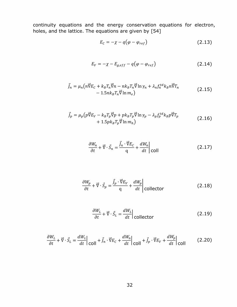
32
continuity equations and the energy conservation equations for electron,
holes, and the lattice. The equations are given by [54]
𝐸𝐶 = −𝜒 − 𝑞(𝜑 − 𝜑𝑟𝑒𝑓) (2.13)
𝐸𝑉 = −𝜒 − 𝐸𝑔,𝑒𝑓𝑓 − 𝑞(𝜑 − 𝜑𝑟𝑒𝑓) (2.14)
𝐽 𝑛 = 𝜇𝑛(𝑛∇ 𝐸𝐶 + 𝑘𝐵𝑇𝑛∇ 𝑛 − 𝑛𝑘𝐵𝑇𝑛∇ ln 𝛾𝑛 + 𝜆𝑛𝑓𝑛
𝑡𝑑𝑘𝐵𝑛∇ 𝑇𝑛
− 1.5𝑛𝑘𝐵𝑇𝑛∇ ln𝑚𝑒) (2.15)
𝐽 𝑝 = 𝜇𝑝(𝑝∇ 𝐸𝑉 − 𝑘𝐵𝑇𝑝∇ 𝑝 + 𝑝𝑘𝐵𝑇𝑝∇ ln 𝛾𝑝 − 𝜆𝑝𝑓𝑝
𝑡𝑑𝑘𝐵𝑝∇ 𝑇𝑝
+ 1.5𝑝𝑘𝐵𝑇𝑝∇ ln𝑚ℎ) (2.16)
𝜕𝑊𝑛
𝜕𝑡+ ∇ ∙ 𝑆 𝑛 =
𝐽 𝑛 ∙ ∇ 𝐸𝐶
q+
𝑑𝑊𝑛
𝑑𝑡|coll
(2.17)
𝜕𝑊𝑝
𝜕𝑡+ ∇ ∙ 𝑆 𝑝 =
𝐽 𝑝 ∙ ∇ 𝐸𝑉
q+
𝑑𝑊𝑝
𝑑𝑡|collector
(2.18)
𝜕𝑊𝐿
𝜕𝑡+ ∇ ∙ 𝑆 𝐿 =
𝑑𝑊𝐿
𝑑𝑡|collector
(2.19)
𝜕𝑊𝐿
𝜕𝑡+ ∇ ∙ 𝑆 𝐿 =
𝑑𝑊𝐿
𝑑𝑡|coll
+ 𝐽 𝑛 ∙ ∇ 𝐸𝐶 +𝑑𝑊𝑛
𝑑𝑡|coll
+ 𝐽 𝑝 ∙ ∇ 𝐸𝑉 +𝑑𝑊𝑝
𝑑𝑡|coll
(2.20)

33
𝑆 𝑛 = −5𝑟𝑛𝜆𝑛
2(𝑘𝐵𝑇𝑛
𝑞𝐽𝑛 + 𝑓𝑛
ℎ𝑓𝑘𝑛∇ 𝑇𝑛) (2.21)
𝑆 𝑝 = −5𝑟𝑝𝜆𝑝
2(−
𝑘𝐵𝑇𝑝
𝑞𝐽𝑝 + 𝑓𝑝
ℎ𝑓𝑘𝑝∇ 𝑇𝑝) (2.22)
𝑆 𝐿 = −𝑘𝐿 ∇ 𝑇𝐿 (2.23)
𝑘𝑛 =𝑘𝐵
2𝑛𝜇𝑛𝑇𝑛
𝑞 (2.24)
𝑘𝑝 =𝑘𝐵
2𝑝𝜇𝑝𝑇𝑝
𝑞 (2.25)
Equations (2.13) and (2.14) represent the conduction and valence band
edges. The current densities are given by equations (2.15) and (2.16), where
𝑇𝑛 and 𝑇𝑝 are the carrier temperatures whereas 𝐸𝐶 and 𝐸𝑉 are the conduction
and valence band potentials, respectively. The first two terms take into
account the contribution due to the spatial variations of electrostatic potential,
electron affinity, and the energy bandgap. The three left terms take into
account the contribution due to the gradient of concentration, the carrier
temperature gradients, and the spatial variation of the effective masses 𝑚𝑒
and 𝑚ℎ. For Fermi statistics, 𝛾𝑛 and 𝛾𝑝 are given by 𝛾𝑛 = 𝑛 exp(−𝜂𝑛) 𝑁𝐶⁄ and 𝛾𝑝 =
𝑝 exp(−𝜂𝑝 ) 𝑁𝐶⁄ , with 𝜆𝑛 = 𝐹1 2⁄ (𝜂𝑛) 𝐹−1 2⁄ (𝜂𝑛)⁄ and 𝜆𝑝 = 𝐹1 2⁄ (𝜂𝑝) 𝐹−1 2⁄ (𝜂𝑝)⁄ and, 𝜂𝑛 =
(𝐸𝐹,𝑛 − 𝐸𝐶) (𝑘𝐵𝑇⁄ ), 𝜂𝑝 = (𝐸𝑉 − 𝐸𝐹,𝑝) (𝑘𝐵𝑇⁄ ). 𝐹1 2⁄ and 𝐹−1 2⁄ are the Fermi integral of
order ½ and -½, respectively. For Boltzmann statistic, 𝛾𝑛 = 𝛾𝑝 = 𝜆𝑛 = 𝜆𝑝 = 1.
The energy balance equations are given in equations (2.17) and (2.18)
while equations (2.21) to (2.23) represent the energy flux [54]. 𝑓𝑛ℎ𝑓
and𝑓𝑝ℎ𝑓
are
the coefficients for heat flux, 𝑓𝑛𝑡𝑑and 𝑓𝑝
𝑡𝑑 are the coefficients for thermal
diffusion, 𝑟𝑛 and 𝑟𝑝are the coefficients for energy flux.
The drift-diffusion carrier transport model takes into account carrier
velocity and lifetime, bias voltage, and optical field intensity, while the
hydrodynamics carrier transport also takes into account carrier temperature

34
dependent parameters such as mobilities and diffusion coefficients and thereby
models more accurately the carrier transport.
The DDCTM is valid as the absorption and collection layers lengths (𝐿𝑎 =
220 nm and 𝐿𝑐 = 263 nm) are too lower when compared with their respective
electron-phonon scattering lengths (𝐿 ≫ 𝐿𝑒−𝑝ℎ, 𝐿𝑒−𝑝ℎ,𝑎 ≅ 16 and 𝐿𝑒−𝑝ℎ,𝑐 ≅ 7.9 nm,
respectively) [79]. The HDCTM is valid as the length device are too lower when
compared with the electron-electron scattering length (𝐿 ≫ 𝐿𝑒−𝑒). Under this
situation, the simulation is valid because the absorption and collection layer
lengths (𝐿𝑎 = 220 nm and 𝐿𝑐 = 263 nm) are too larger when compared with their
respective electron-electron scattering lengths (𝐿𝑒−𝑒,𝑎 ≅ 1.3 nm and 𝐿𝑒−𝑒,𝑐 ≅ 1.0
nm) [79]. See Appendix C to see the procedures used in the computing of the
different relevant scattering lengths.
2.1.3. Numerical results from DD and HD Model
This section will show several simulation results using the drift-diffusion
and hydrodynamic model of the InGaAs/InP UTC-PD structure shown in Table
2.1. DC simulations were performed under different input optical power. Figure
2.2 shows the responsivity curve for the 3 and 10 m diameter cylindrical
devices. Figure 2.2 also shows also the responsivity curve reported in
reference [80], which is a 5-m diameter cylindrical device. The responsivity
is a common measure of the photodetector performance, which is defined as
the ratio of the photocurrent to the optical intensity (see equation (1.2)). The
InGaAs/InP UTC-PD responsivity was also investigated by varying the optical
intensity from 5×10³ W/cm2 to 1×10⁷ W/cm2, under an applied reverse voltage
of 2 V. Under low-level illumination, the 10-m InGaAs/InP UTC-PD device
presents a responsivity of 0.13 A/W, and the 3-m InGaAs/InP UTC-PD device
present a 0.17 A/W. With high-level illumination, the 10-m InGaAs/InP UTC-
PD device responsivity falls abruptly at 5×10⁵ W/cm2, while the 3-m
InGaAs/InP UTC-PD device responsivity falls at 3×10⁵ W/cm2. Therefore, the
devices with greater surface supports higher optical intensity but with lower
responsivity. The 3-m and 10-m diameter LE-UTC gives maximum of
responsivity values of 0.2 and 0.14 A/W, respectively. These values are not
far from 0.25 A/W reported by Mahmuddur Rahman et al [80], performing

35
hydrodynamic simulations with a 5-m-diameter LE-UTC photodiode. Figure
2.3 shows the same as Figure 2.2, but with the optical input expressed in W.
Figure 2.2. Plot of responsivity of the LE-UTC photodiode versus optical
intensity for the 3, 5, and 10 m diameter under an applied reverse bias of
2 V. The results for the 5-m LE-UTC were taken from reference [80]

36
‘
Figure 2.3. Responsivity of the InGaAs/InP UTC-PD device versus optical
intensity for for a 3 and 10 m diameter device under a reverse bias of 2 V.
For the sake of simplicity and the purpose of this thesis, a definition of
curvature is given here. The curvature is the reciprocal of the radius of a circle.
Therefore, the curvature of a circle of radius R is small if R is short and small
if R is long. Following this, one says, the higher is the curvature, more is the
bending. Figure 2.4 shows the energy band diagrams for a 3 m diameter UTC-
PD device under different optical injection levels at a reverse bias of 2 V. Figure
2.4 also shows the distance corresponding to the absorption, cliff, and
collection layers. Under low-level optical-input injection (optical injection with
values lower than 1 × 10⁵ 𝑊/𝑐𝑚2), the curvature value of the collection bandgap
is practically zero (no bending). Under high-level optical-input injection, this
value increases (bending start to appears). This band-bending phenomenon is
in agreement with published results [81]. An interesting feature of this bending
appears as the optical intensity increases from 2.5 × 10⁶ 𝑊/𝑐𝑚2 to 1 ×
107 𝑊/𝑐𝑚2: the curvature value decreases making the collection bandgap
practically linear. This behavior suggests that the cliff layers as the main cause
why the energy bandgap deviates that much from its shape under low-level
optical-input injection. In the following, more results will be shown to support
this conjecture The cause of this behavior appears to happen in the cliff-layers,
where first a reduction of the gradient and then a reversal of the electrical field
occurs for the electrons in the conduction band (but only a minor reduction for

37
the holes in the valence band) as the optical intensity is increased to the
highest value of 1 × 10⁷ 𝑊/𝑐𝑚2 [50]. Until 104 𝑊/𝑐𝑚2 only marginal changes
occur.
Figure 2.4. Energy band-diagram for different optical injection levels, the line style matches the optical intensity for each curve for both, the valence
and conduction bands.
To understand better this reduction in the electrical field, the electric field
profile is shown in Figure 2.5 for different optical intensities with an applied
reverse bias of 2 V. Figure 2.5a) shows the calculated electric fields for optical
intensities between 5×10³ and 5×10⁵ W/cm2. Figure 2.5b) shows the
calculated electric fields for optical intensities between 5×10⁵ and 1×10⁷
W/cm2. The electric field is nearly zero in the heavily doped absorption and
subcollector regions, it peaks at the junctions between the p-contact and block
layers, block layer and absorption layer, absorption layer and cliff layers, and
between the collection and subcollector layers.
At low light levels, the electric field inside the cliff layers, as shown in
Figure 2.5a), is higher than present at high light levels as shown in figure
Figure 2.5b). To understand better, the nature of this decreasing electric field
inside the cliff layers when a strong optical input is applied, Figure 2.6 shows
the space charge vs distance plot. When the light conditions change from low

38
to high level, the space charge inside the cliff layers increases strongly. This
is explained by the accumulation of electrons around the pikes present at the
cliff layer energy bandgap.
Under low light levels (between 5×10³ and 7.5×10⁴ W/cm2) (see Figure
2.5a), the electric field inside the collector layer has a negative slope. When
the optical intensity is increased again to 5×10⁵ W/cm2, the slope of the
electric field inside the collector layer changes from a slightly negative to a
slightly positive value. During this increasing optical intensity, the electric field
inside the cliff layers is clearly lower and its maximum peak decreases from
1.5×10⁵ to 1.2×10⁵ V/cm. For high light levels (between 5×10⁵ and 1×10⁷
W/cm2), the slope of the electric field inside the collector retains its positive
value, leaving the electric field fixed at the collection layer end and increasing
their its value close the cliff layers as shown in Figure 2.5b. At high light levels
also accentuates the decreasing nature of the electric field inside the cliff layers
as showed in Figure 2.5b. This behavior can be explained with the help of
Figure 2.7, which shows the electron density vs distance present along the
structure layer of the UTC-PD device. For low light levels (up to 7.5×10⁴
W/cm2), the electron density is similar in value in both layers, the absorption
and collection layer. Under this condition, the electric field has a positive slope
as shown in Figure 2.5a). With optical intensities larger, like 5×10⁵ W/cm2, the
electrons start to accumulate at the absorption layer changing the space
charge profile. To explain this behavior, the conjecture that the band bending
is due to the cliff layers, as proposed in Figure 2.4, will be resumed. Observing
the cliff layers in Figure 2.7, the electron density has values similar to those
from the absorption and collection layers under conditions of low-level lights.
Under high-level light conditions, the accumulation of electrons in the cliff layer
is greater than the electron density at the absorption and collection layers
having an effect of electron trapping at the absorption layer. Therefore, the
space charge effect is strongly influenced by the cliff layers. This suggest a
route in improving future UTC-PD devices by engineering the cliff layers in
order to smooth the transition between absorption and collection layer. One
possibility is the Other way to do improvement in the UTC-PD devices is the
suggestion of a homojunction between the absorption layer to suppress the
cliff layers making the transition totally smooth, but this is not possible
because it is needed to avoid electron-hole generation inside the collection
layer. This is, the collection layer needs to be completely transparent to the
wavelength of operation. A third way to solve this issue was the use of a
staggered heterojunction (type II). The lattice-matched GaAs0.51Sb0.49 instead
of In0.53Ga0.47As in the UTC-PD absorption layer was used [82]. The GaAsSb
absorbing layer conduction band edge lines up Δ𝐸𝐶 = 0.11 eV above that of InP,
making a type-II heterojunction with the InP collection layer. This allows

39
avoiding the compositional grading layer between the absorption and collection
layer simplifying the UTC-PD final structure and suppressing the conduction
band energy peaks between the absorption and collection layer of the InGaAs-
InP UTC-PD [82]. Therefore, space charge limitation is suppressed.

40
a)
b)
Figure 2.5. Electric field under different optical power. a) Optical intensities from 5 × 10³ and 5 × 10⁵ W/cm2. b) 5 × 10⁵ and 1 × 10⁷ W/cm2.

41
a)
b)
Figure 2.6. Space charge under different optical power. a) Optical intensities from 5 × 10³ to 7.5 × 10⁴ W/cm2. b) from 5 × 10⁵ to 1 × 10⁷ W/cm2.
At enough high optical power levels, the space-charge-induced electric
field is strong enough to collapse the external electric field. This leads to a
decrease in the transit time (and corresponding decreasing in bandwidth), a

42
reduction in the saturation photocurrent. The number of photogenerated
carriers that travels through the UTC photodiode also increases enough to
increase the space charge inside the cliff layers. This leads to a screening effect
on the electrons traveling across the device, decreasing the saturation
photocurrent and electron velocity (decreasing in bandwidth).
Figure 2.7. Electron density versus distance under different optical intensities.
Figure 2.8a shows curves of electron velocity against the distance
measured from the block layer. Three plots are presented, two resulted from
the HDCTM and, the other plot from the Drift-Diffusion Carrier Transport Model
(DDCTM). The simulated DDCTM plot was compared with the reported by
Rahman et al [80], and they are exactly the same results. Then, only one
DDCTM plot was depicted in Figure 2.8a. The HDCTM predicts velocity
overshoot, which is observed in Figure 2.8a when this is compared with the
results from the DDCTM. The velocity overshoot is present because the DDCTM
only predicts a saturated velocity [80]. The physical origins of the velocity
overshoot is shown in Figure 2.9. This figure shows the measured electron drift
velocity versus the applied electric field for InGaAs. In low electric field regime
(0-1 kV/cm), the electron velocity increases proportional to the electric field.
This region has a linear dependence a represented by the dashed line. In this
electric field regime, the conduction electrons are in the high-mobility energy
minimum (called a valley) represented by the lower valley (see inset 1). If the
electric field is increased more than the electric linear regime, the electric field
delivers an additional energy Δ𝐸 to the conduction electrons. As a result, the

43
electrons are transferred to the upper valley, where the electron mobility is
lower (see Figure 2.9, inset 2) [83, pp. 73–75].
An interesting feature shown by our simulation, which is presented in
Figure 2.8a, is the electron overshoot appearing at the absorption layer,
contrary to the prediction by the DDCTM, which guesses a lower electron
velocity. The electron velocity starts increasing in the absorption layer and it
almost reaches a maximum velocity of 4 × 107 cm/s value close the cliff layers.
This is explained in Figure 2.10 and Figure 2.9. Figure 2.10 is a plot of Electric
field vs distance like Figure 2.5. The difference is the vertical axis are limited
between 0 and 4 kV/cm to zoom the electric field at the absorption layer. The
electric field has values that go from 2.5 × 10⁻² to 3 kV/cm, and according to
Figure 2.9, the electron energy falls in the lower valley where the electrons
have the highest mobility. Therefore, velocity overshoot occurs in the
absorption layer. The electron velocity starts with its maximum value
decreasing as the electron travels along the collection layer. This lower velocity
is explained qualitatively in Figure 2.9. According to Figure 2.5, the collector
electric field values oscillates around 65 and 160 kV/cm, which means that the
electrons operate in the electron-velocity saturated regime. Therefore, the
electrons populate completely the upper valley with lower mobility.
Additionally, the electron velocity shows a monotonically decrease in the
collection layer, according to our results. This is explained qualitatively with
the help of the Figure 2.8b. Figure 2.8b shows the electron temperature versus
the distance. The maximum electron temperature appears to be at the
collection layer. The electron temperature is a measurement of the kinetic
energy of the electrons. It is clearly that the maximum electron kinetic energy
appears across the collection layer.
A comparison between Figure 2.8a and Figure 2.8b, our simulation shows
an apparently contradiction between the electron velocity and the kinetic
energy of the electrons, because the absorption layer presents the maximum
electron velocity, the electron temperature is the lowest among the whole
structure. Contrary to this, the collection electron velocity is decreasing and
has the highest electron temperature. This is explained qualitatively in the
following manner. At any finite temperature above the absolute zero, the free
electrons are in a random motion inside the lattice, and due the imperfections
originated in the thermal lattice vibration, the electrons are colliding with the
lattice atoms. The average of all the free paths taken by the electrons between
successive collisions is the mean free path, 𝑙, and associated with this value is
the mean free flight time, , which is calculated as 𝜏 = 𝑙 𝑣𝑇⁄ , where 𝑣𝑇 =
√2𝑘𝐵𝑇 𝑚𝑒⁄ is the thermal velocity of the electrons, 𝑘𝐵 is the Boltzmann’s
constant, 𝑚𝑒 is the electron mass (9 × 10⁻²⁸ g), and 𝑇 is the absolute

44
temperature taken a room temperature (usually taken at 300 K, the room
temperature). The mean free flight time is interpreted as the time for which
an electron is allowed to freely accelerate and build up a superposed velocity
(over and above its thermal velocity) and hence a superposed displacement.
When a small electric field is applied, the electrons receive an additional
energy, it is shared with the lattice in the form of collisions. Anyway, the
probability of a collision and the mean free time, 𝜏, are not affected by this
small increase in electron velocity. However, when the electric field applied to
a semiconductor is increased significantly (higher than 69 kV/cm), the electron
velocity between two successive collisions inside the collection layer is
increased significantly over the thermal velocity 𝑣𝑇 according Figure 2.5.
Therefore, the probability of the electron encountering a collision increases,
leading to a reduction of mean free flight time (𝜏) and electron mobility 𝜇𝑛
[77]. As the electric field becomes more intense, the number of collisions
increases, implying that the charge carriers increase the intensity of their
interaction with the lattice potential, and that means that they become
heavier. Therefore, their kinetic energy is increased by increasing the electron
mass from the standpoint of the system, but their velocity is lower.
The first difference is the higher electron velocity inside the block layer.
But, this has to be discarded because its role is to block the electron passing
through this layer. Therefore, there is not a physical meaning off the electron
velocity magnitude inside this layer. This thesis also reports a slightly higher
electron velocity across the absorption layer than the reported by Rahman et
al. Therefore, there is not a significant difference between them. Across the
collection layer, the physical behavior is different. According to Rahman et al,
the electron velocity starts decreasing up to reaching a minimum at some
position of the collection layer. After this position, the electron velocity starts
to increase its magnitude reaching a new local maximum to decrease after
reaching such position. This thesis reports a different physical behavior for the
electron velocity across the collection layer. In this case, the electron velocity
starts with a maximum at the beginning of the collection layer. After this
maximum, the electron velocity is always decreasing. A comparison between
Figure 1.5 and Figure 2.5 justify this behavior. Figure 2.5 shows that the
maximum velocity appears when the electric field is about 13 kV/cm (for InP,
because this is the collection layer material), while the electric field inside the
collection layer has values higher than the electric field for the maximum
electron velocity of the InP materials. This means that the electron velocity
has to be valued lower than the maximum electron velocity at the collection
layer, and looking the electron temperature in Figure 2.8b, the number of
collisions of electrons inside the collection layer should be the highest among

45
the whole UTC photodiode. Therefore, the electron velocity has to be a
decreasing fashion at the collection layer.
a)
b)
Figure 2.8. a) Electron velocity distribution where the reported results were
obtained from S.M. Mahmudur Rahman et al [80], and b) electron temperature across the UTC-PD at a 2 V reverse bias and optical intensity of
5000 W/cm2, also compared with the reported results in reference [80].

46
Figure 2.9. Physical principle of the transferred-electron effect: The main
plot shows the Electron velocity vs the applied electric field. The linear dashed shows the linear region where the electron velocity behaviors
linearly. Under this situation the electrons remain in the lower valley (inset 1). At electric field values higher than 1 kV/cm, the electrons start to
transfers from the lower valley to the upper valley represented in the figure
inset 2 [76].

47
Figure 2.10. Electric field versus distance under different applied optical
intensities. This plot corresponds to figure Figure 2.5a, but with a vertical
axis scale between 0 and 4 × 10³ V/cm, to focus on the electric field inside
the absorption layer.
Despite there are simulation results, the results here presented are really
reported results [80], and therefore not relevant to publish. The initial goal
was simulating different layers’ thickness to study the performance behavior,
and also the transient, and AC response of the LE UTC devices but they were
not possible due to numerical convergence.

48
3. RF Electromagnetic Modeling
RF electromagnetic modeling is used in general as design tool, but in this
thesis, the purpose of RF electromagnetic modeling is to understand the THz
losses from physical principles. Therefore, by the help of RF electromagnetic
modeling tools, it is expected to be understood the influence of THz losses in
VI-TW-UTC photomixers. This chapter will give a short review about the time-
domain modeling and the corresponding tool used for this purpose. This will
give also a short explanation about the tool used for the frequency domain
modeling.
3.1. Time-domain modeling (CST Microwave Studio)
The Transient solver used in CST Microwave Studio is based on the Finite
Integration Technique (FIT). It applies highly advanced numerical techniques
like the Perfect Boundary Approximation (PBA)® in combination with the Thin
Sheet Technique™ (TST) to allow accurate modeling of small and curved
structures without the need for an extreme refinement of the mesh at these
locations. This allows a memory-efficient computation together with a robust
hexahedral meshing to successfully simulate extremely complex structures.
The fields are calculated step by step through time by the “Leap Frog” updating
scheme [85]. It is proven that this method remains stable if the step width for
the integration does not overcome a known limit. This value of the maximum
usable time step is directly related to the minimum mesh step width used in
the discretization of the structure. Therefore, a denser means a smaller time
step size [86].
3.2. Frequency domain modeling (HFSS)
To calculate the full three-dimensional electromagnetic field inside a
structure and the corresponding S-parameters, HFSS employs the finite
element method (FEM) [87]. FEM is a very powerful tool for solving complex
engineering problems, the mathematical formulation of which is not only
challenging but also tedious. The basic approach of this method is to divide a
complex structure into smaller tetrahedral sections known as finite elements.
These elements are connected to each other via joint scaled nodes. Each
unique element is then solved independently of the others thereby drastically
reducing the solution complexity. The final solution is then computed by
reconnecting all the elements and combining their solutions. These processes
are named assembly and solution respectively in the FEM [87]. FEM finds
applications not only in electromagnetics but also in other branches of
engineering such as plane stress problems in mechanical engineering,
aerodynamics and heat transfer.

49
FEM is the basis of simulation in HFSS. HFSS divides the geometric model
into a large number of tetrahedral elements. Each tetrahedron is composed of
four triangles and the collection of tetrahedral forms what is known as the
finite element mesh. Figure 3.1 shows the finite element mesh for a sample
horn antenna. This figure was taken from [87]. At each vertex of the
tetrahedron, components of the field tangential to the three edges meeting at
that vertex are stored. The other stored component is the vector field at the
midpoint of selected edges, which is also tangential to a face and normal to
the edge. Using these stored values, the vector field quantity such as the H-
field or the E-field inside each tetrahedron is estimated. A first-order tangential
element basis function is used for performing the interpolation. Maxwell’s
equations are then formulated from the field quantities and are later
transformed into matrix equations that can be solved using traditional
numerical techniques.
Figure 3.1. Procedure used by HFSS in order to solve an electromagnetic
problem [87].
3.3. Electromagnetic simulation results for TW-mixer
structures in different simulators
3.3.1. Port-to-Transmission-line transmission losses and impedance
matching
The procedure used to get the best value for the characteristic impedance
𝑍0 of the CPW at which the power from port 1 is transferred best to the
waveguide, and extracted from it in port 2 is shown in Figure 3.2. We start by
giving an arbitrary and reasonable initial input 𝑍0 value at the device shown in
Figure 3.10. The simulations were performed in the time domain (see Figure
3.4b), then the smith chart with the scattering 𝑆11 parameter for each
conductivity is created and inspected. If the 𝑆11 curve is far from the
intersection between the 𝑍0 = 1 circle and the horizontal axis, a new value for
𝑍0 is proposed and then simulated. This is repeated up to find the 𝑍0 value for
which the 𝑆11 curve is the closest to the intersection between the 𝑍0 = 1 circle

50
and the horizontal axis (see Figure 3.3). This procedure and its results are
shown in Figure 3.4. The program CST Microwave Studio™ was manually
stopped after the seed pulse coupled in completely.
Figure 3.2. Flowchart diagram explaining the procedure to get the best
characteristic impedance of the transmission line by simple visual inspecting of the Smith Chart.

51
Figure 3.3. Smith chart showing the results of the procedure depicted in
Figure 3.2.

52
Figure 3.4. a) Port 1 impedances versus conductivity determined by
centering the Smith chart (left inset) using CST Microwave Studio™ in the pulsed domain with a frequency range of 0 − f2, with f2 = 1, 2, or 4000 GHz. There was the problem that the reflected pulse was not anymore Gaussian
for f2 > 1000 GHz in b). These values were confirmed in HFSS™.

53
3.3.2. Dependence of the dark THz-absorption on the base n-layer
conductivity
Two types of waveguides have been used for sub-mm and THz generation.
The first type of waveguide consists of planar metal-semiconductor-metal
(MSM) CPS for (non-polar) one-layer photoconductors where the electron-trap
phenomenon dominates (e.g. LT-GaAs). The second type of waveguide
illustrated in Figure 3.5(a) and (b), is a coplanar waveguide (CPW) for polar
vertical (mesa) photodiode semiconductor structures where the transit time
phenomenon dominates (e.g. the InGaAs/InP system). In this second case,
the mesa structure is contained under the central stripline.
Figure 3.5. Photodiodes fabricated in the form of mesa structures grown
on semiconductor substrates, a) p-i-n and b) UTC (simplified). There are two limiting cases for these structures, one where the n-layer becomes a
dielectric (𝜎 = 0) (c), and the other when it becomes a perfect conductor
(d).
In the first analytical and simulated evaluations of TW photodiodes [27],
the signal-collecting microwave waveguide was regarded as a vertical MSM
microstrip waveguide, which is a vertical arrangement of metal stripline
followed by a semiconductor layer and again a metal stripline (“a vertical
sandwich MSM”). However, since semiconductor layers cannot be grown on a
metal bottom layer, they can only be realized through a flip-chip process [88]
which further complicates the already difficult fabrication process. Therefore,
the bottom conductor stripline of the vertical (mesa) structure is normally
realized by a highly doped semiconductor layer (n-layer in Figure 3.5),
connecting the central mesa structure to the outer metal CPW-striplines. For
either p-i-n or UTC lumped-element and TW photodiodes, this doping was
usually taken in the range of 1 × 1019 cm-3 [39][50], roughly corresponding to
a conductivity of 1.6 × 10⁵ S/m [50]. Figure 3.5 shows these two types of
photodiodes. Therefore, this conductivity range was analyzed so as to find an
absorption in the sub-mm and THz range as low as possible, i.e. for obtaining
the highest possible THz output power. The n-layer in Figure 3.5 is the
underlying doped layer for which the effect of changing the conductivity is
investigated in this work.

54
The Drude model, 𝜎(𝑛𝑒) = 𝑒 ⋅ 𝜇(𝑛𝑒) ⋅ 𝑛𝑒, can be used to estimate the
conductivity, assuming that the electron concentration equals the doping
concentration. The decaying tendency of the mobility, μ(ne), as a function of
doping, can be estimated for example from Kopf et al. [89].
However, the full-wave simulations described in the present paper work
with the conductivity 𝜎. The correct conversion in doping levels is secondary
and not analyzed further here. In the simulations presented, the conductivity
range corresponds roughly to a carrier concentration range from 1012 cm-3
(intrinsic semiconductor) to 1022 cm-3 (value for gold). Such very high doping
values cannot be reached in a practical semiconductor since structural
problems will occur. Doping levels as high as 7 × 1019 cm-3 can be achieved in
InP, and 5 × 1019 cm-3 in InGaAs, using metal organic chemical vapor phase
deposition (MOCVD) [90].
By varying the conductivity of this n-layer from 0 to ∞, the effective
waveguide structure changes from a quasi-planar co-planar waveguide (Figure
3.5c) to a vertical microstrip arrangement (Figure 3.5d). Since the i-layer is
ideally an insulator, both limiting cases have low losses. However, the
intermediate cases, the real cases of p-i-n or UTC-TW photodiodes with
intermediate conductivity in the n layer, should have higher losses. This can
be understood as follows. Generally, the ohmic losses per length unit result
from the cross-sectional overlap of electric field and current density pattern
𝑗 (𝑟 ),
𝑣𝑝ℎ ∙𝑑𝑊
𝑑𝑧=
𝑑𝑊
𝑑𝑡≈ −∫𝑗 ⋅ 𝑑𝑉
𝑉
≈ −∫𝜎(𝑟 )𝑉
⋅ | (𝑟 )|2𝑑𝑉
≈ −𝜎 ∫| (𝑟 )|2𝑑𝑉 ≈ −
2𝜎
휀0휀𝑊
𝑉
, (3.1)
where 𝑊 = 𝜖0 2⁄ ∙ ∫ 휀(𝑟 )| (𝑟 )|2𝑑𝑉
𝑉≈ 𝜖0 2⁄ ∙ ∫ | (𝑟 )|
2𝑑𝑉
𝑉 is the energy stored in a
volume 𝑉 with a sufficiently large cross section, 𝐴, outside of which the field
can be neglected. The length of the test volume may be chosen to be half of
the wavelength to account for one whole current pattern, i.e. 𝑉 = 𝐴 ∙ 𝜆/2. Then,
we can write 𝑑𝑊 𝑑𝑧⁄ = −𝛼𝑊, where 𝛼 = 2 𝑐𝜖0√휀⁄ is the absorption constant.
Note that 𝜎, the average conductivity, increases first with low values of 𝜎. In
contrast, 𝜎 does not necessarily increase when 𝜎 increases further in sub-
volumes (high-doping areas and metal contacts), since the penetration depth
of the electric field is increasingly reduced (skin depth effect), so that the
overlap integral is dominated by the intermediate and low conductivity areas.
This expression may also provide the possibility to determine the absorption
constant directly from the numerical electric field and current density solution
or the 𝜎 profile at a specific position on the transmission line. However, for

55
high conductivities, the spatial resolution required in the thin overlap regions
between high E-field (and low current density) and low E-field (and high
current density) must be appropriately high to obtain a sufficiently precise
numerical solution in this way. This constitutes a difficulty in terms of
computational time, so that in praxis we could not show that this method
produces consistent results.
The way the waveguide losses develop when the underlying “sub-
collector” n layer changes from an insulating layer to a perfectly conducting
one, is therefore investigated in the present work by using full-wave
simulations in two different simulation platforms via Ansoft’s High Frequency
Structural Simulator (HFSS™) and CST’s Microwave Studio™.
These simulations were originally deemed worthwhile because a previous
experiment, with travelling-wave photomixers based on planar electrodes on
LT-GaAs, revealed increased sub-mm transmission-line losses when the free-
electron density below the transmission line was increased by optical
absorption [91].
We first develop an idealized analytical transmission line model and derive
the model parameters from first principles. Then we describe the structural
model used for the simulations and compare the absorption constant results
obtained with two different methods.
3.3.2.1. Analytical Model
A simplified analytical model of the structures, presented in Figure 3.6
was set up to support the full-wave analysis described further below. Although
the analytical model is not showing all the features of the full-wave analysis,
it still justifies the overall behavior.
Note that in the following analysis no radiation losses (Poynting vector)
are included. From the simulation results and from earlier work [6][92] it can
be seen that they are small in comparison with the level of absorption losses
discussed here. Nevertheless, they complicate the simulations and are
discussed accordingly.

56
Figure 3.6. a) Conductances and capacitances represented on the
waveguide. b) Voltage and current definitions and equivalent circuit for an incremental length ∆𝑧 of transmission line. The reduced geometry is obtained
from the symmetry in a).
Figure 3.6a shows the cross-section of a waveguide structure, which
represents the intermediate cases between a coplanar waveguide and a
microstrip line. In the cross-section, the equivalent conductances and
capacitances, taken into account in the analytical model, are represented. A
longitudinal representation of an infinitesimal Δ𝑧-length section of this
waveguide is illustrated in Figure 3.6b. Its cross-sectional symmetry can be
modeled as a lumped-element circuit for which the following quantities per
unit of length are defined:
𝑅1 and 𝑅2 = series resistances,
𝐿1 and 𝐿2 = series inductances,
𝐺1 and 𝐺2 = shunt conductances,
𝐶1 and 𝐶2 = shunt capacitances.
The series inductances 𝐿1 and 𝐿2 represent mainly the mutual inductances
between the two inner striplines and the ground line (outer CPW striplines),
respectively. On the other hand, the mutual inductance between the two inner
striplines is neglected due to a much lower separation. A finite length of the
waveguide is viewed as a series of sections of the form shown in Figure 3.6b.
The replacement geometry in Figure 3.6b is now equivalent to an
asymmetric CPW. Although the Eigen-modes of a symmetric CPW (as in Figure
3.6a) are the symmetric mode and the anti-symmetric mode, those of an
asymmetric one (as in Figure 3.6b) should be hybrid combinations of both.
The following linear differential equation system is established:

57
[ 𝑑𝑉1(𝑧) 𝑑𝑧⁄
𝑑𝑉2(𝑧) 𝑑𝑧⁄
𝑑𝐼1(𝑧) 𝑑𝑧⁄
𝑑𝐼2(𝑧) 𝑑𝑧⁄ ] = [
0 0 𝐴 𝐵0 0 0 −𝐵𝐶 0 0 0
−𝐶 𝐷 0 0
]
[ 𝑉1(𝑧)
𝑉2(𝑧)
𝐼1(𝑧)
𝐼2(𝑧)] with
𝐴 = −(𝑅1 + 𝑗𝜔𝐿1)
𝐵 = −(𝑅2 + 𝑗𝜔𝐿2)
𝐶 = −(𝐺1 + 𝑗𝜔𝐶1)
𝐷 = −(𝐺2 + 𝑗𝜔𝐶2).
(3.2)
The normalized general solution of this system for one propagation
direction, determined in Matlab™ using symbolic evaluation, is given by:
[ 𝑉1(𝑧)
𝑉2(𝑧)
𝐼1(𝑧)
𝐼2(𝑧)] = 𝑐1
[ 𝛾1
𝛾12 + 𝐵𝐶 + 𝐵𝐷
𝐴𝐶2
𝛾1
𝛾12 + 𝐵𝐶 − 𝐴𝐶 + 𝐵𝐷
𝐴𝐶𝐷
−𝛾1
2 + 𝐵𝐶 + 𝐵𝐷
𝐴𝐶1 ]
𝑒−𝛾1𝑧
+ 𝑐2
[ 𝛾2
𝛾22 + 𝐵𝐶 + 𝐵𝐷
𝐴𝐶2
𝛾2
𝛾22 + 𝐵𝐶 − 𝐴𝐶 + 𝐵𝐷
𝐴𝐶𝐷
−𝛾2
2 + 𝐵𝐶 + 𝐵𝐷
𝐴𝐶1 ]
𝑒−𝛾2𝑧
(3.3)
where the two complex propagation constant distinguish two wave modes and
are given by:
𝛾𝑞(𝑓, 𝜎) = 𝛼𝑞(𝑓, 𝜎) + 𝑗𝛽(𝑓,𝜎)
=√𝐴𝐶
2∓
√𝐴2𝐶2 − 2𝐴𝐵𝐶2 + 2𝐴𝐵𝐶𝐷 + 𝐵2𝐶2 + 2𝐵2𝐶𝐷 + 𝐵2𝐷2
2−
𝐵𝐶2
−𝐵𝐷2
(3.4)
where the subscripts 𝑞 = 1,2 refers to complex propagation constant 1 and 2.
𝛼𝑞 is the absorption constant and it arises from Ohmic losses in the conductors
and the dielectric materials. The dielectric losses dominate when the substrate
is highly conductive due to, for example, free carriers coming from the doping
of the semiconductor substrate. 𝛽𝑞 is the phase constant, and it determines
the degree of dispersion a signal experiences, and it is affected primarily by
the geometry of the transmission line, its dimensions, and the substrate
permittivity. The two solutions obtained for the two complex propagation
constants, 𝛾1 and 𝛾2, correspond to two different propagation modes. This
section will show that the second mode has a much higher absorption constant
than the first mode which suggests that propagation will occur in the first
mode.

58
Figure 3.7. Cross-sectional view of the CPW structure with relevant parameters. Specific dimensions are given in Table 3.1.
The parameters 𝐺1, 𝐺2, 𝑅1, 𝑅2, 𝐿1, 𝐿2, 𝐶1, and 𝐶2 must be determined to
find the coefficients 𝐴, 𝐵, 𝐶, and 𝐷. The resistances per length, 𝑅1 and 𝑅2, are
found from the gold conductivity of 𝜎 = 4.5 × 10⁷ S/m, using the geometry of
Figure 3.7 and 𝑅 = 𝜌/𝐴 = 1/(𝜎𝐴), where 𝐴 is the area of the transversal cross
section of each conductor. The capacitance 𝐶1 is found from 𝐶1 = 휀0휀𝑟𝑎/𝑡𝑑, where
𝑎 and 𝑡𝑑 are defined in Figure 3.7. The second capacitance per length is given
by 𝐶2 ≈ 𝜋 ∙ (1 + 휀𝑟)휀0𝑠/[2(𝑑 + 𝑠) log[2(1 + √𝜅)/(1 − √𝜅)]], where 휀𝑟 is the relative
permittivity of the substrate, 𝑑 = (𝑐 − 𝑏)/2 ≈ 𝑎 is the electrode width of both
outer conductors, 𝑠 = (𝑏 − 𝑎)/2 is the gap width between the electrodes, and
𝜅 = 1 − tan4[𝜋𝑑/4(𝑑 + 𝑠)]1/2 is a dimensionless quantity [3]. The inductance 𝐿2
is calculated as 𝐿2 = 𝜇0𝑡𝑑2 + ((𝑏 − 𝑎)/2 )21/2/𝑎 [93]. In the same manner, 𝐿1 is
calculated as 𝐿1 = 𝜇0𝑡𝑑/𝑡 [93]. If we regard the layer corresponding to 𝐶1 and
𝐺1 as intrinsic, then we have 𝐺1 = 0. If there is an average photo-illumination,
the conductivity per length can be calculated from the photocurrent per length
as 𝐺1 = 𝜕𝐼𝑝ℎ/𝜕𝑧/𝑉𝑏𝑖𝑎𝑠 while it can also be expressed as 𝐺1(𝜔) ≈ 𝜎𝑖𝑙𝑙𝑢(𝜔) ∙ 𝑎/𝑡𝑑. The
conductance 𝐺2 is estimated as 𝐺2(𝜔) ≈ 𝜎(𝜔) ∙ 𝛿/2𝑠, where 𝛿 ≔ min (𝛿(𝜔), 𝛿𝐷𝐶) is
the minimum function between the skin depth, 𝛿2(𝜔) = 2(√1 + (𝜔휀/𝜎)2 + 𝜔휀/𝜎)/
𝜎𝜔𝜇 [94], and the DC E-field penetration depth, 𝛿𝐷𝐶, which depends only on
the gap 𝑠 and not on the frequency. The ab-initio values of these circuit
parameters are given in Table 3.2, using the geometry of Figure 3.7 and the
dimensions of Table 3.1, where typical dimensions of waveguides used for
microwave, sub-mm, and THz generation are compared. The dimensions of
our waveguide were considered the smallest possible to be reliably reached in
micro-fabrication over larger areas, to access the highest possible frequencies.
Later, the present model is fitted to the simulation results in order to determine
a second set of constants.

59
Table 3.1: Overview of coplanar waveguide parameters used in literature
(b = a + 2s).
Maximum intended
frequency
𝒂 𝒔 𝒄 Mesa
thickness 𝒕𝒅
Metal
thickness 𝒕
Substrate
thickness 𝒕𝒔
Ref.
(GHz) (𝜇m) (𝜇m) (𝜇m) (𝜇m) (𝜇m) (𝜇m) ---
16 12 - 0.1 200 [95]
300 10 10 - 500 [96]
500 36 3 342 - 500 [97]
2000 4 1 (3)* 10 1 0.1 500 our work
* The present study is made with 𝑠 = 1 µm, but 𝑠 = 3 µm is also discussed.
Figure 3.8 summarizes the main results of this model plotted over the
conductivity range 1 × 10⁻¹ − 4.5 × 10⁷ S/m. The absorption constant 𝛼1 is found
to be constant up to 10 S/m, and exhibits a peak beginning well before
1 × 10³ S/m which has an increasing maximum towards higher frequencies
(Figure 3.8a). Up to the conductivity value of that maximum of 𝛼1, 𝛼2 is
constant, but much larger than it, but then begins to increase without limit.
Table 3.2: Parameter values of the analytical model as determined from
material constants and geometry.
Parameter Unit Calculated Value
𝑅1 Ω m⁄ 1.2 × 10⁵ 𝑅2 Ω m⁄ 6.1 × 10⁴ 𝐿1 H m⁄ 4.4 × 10⁻⁷ 𝐿2 H m⁄ 1.3 × 10⁻⁵ 𝐶1 F m⁄ 4.6 × 10⁻¹⁰ 𝐶2 F m⁄ 2.6 × 10⁻¹¹ 𝐺1 S m⁄ 0 or <103 𝐺2 S m⁄ 0.1 − 4.5 × 10⁷

60
Figure 3.8. Analytical solutions for the absorption constants a) 𝛼1 and b)
𝛼2 (real parts of 𝛾1 and 𝛾2) plotted versus conductivity for 0.5, 1.0, 1.5, and
2.0 THz.
Figure 3.9 shows a spectral comparison between 𝛼1 (Figure 3.9a) and 𝛼2
(Figure 3.9b) for various conductivities. The absorption constant 𝛼1 has a
square-root dependence up to a frequency of 10 GHz as shown in Figure 3.9a,
where it starts to saturate. For the conductivity values of 4.8 × 10⁴ and 1.7 ×
105 S/m, it starts to rise again at frequencies of 200 GHz and 300 GHz,
respectively. From that standpoint, higher conductivities seem to be favorable.
In Figure 3.9b it can be seen that 𝛼2 increases linearly for frequencies up to
1 GHz and then with the square-root of the frequency, except for very low
conductivities. 𝛼2 is larger than 𝛼1 starting from a given frequency in the sub-
GHz range where they cross. This crossing frequency decreases as the n-layer
conductivity increases (Figure 3.9c). These findings at low frequencies may
be just of academic interest, as the present article is aimed at the sub-mm
and THz range. Nevertheless, they were followed to find the parameters which
could lead to the identification of the second mode in the simulations.
However, interestingly this was not successful.

61
Figure 3.9. Absorption constant versus frequency for different conductivities
for a) 𝛼1 and b) 𝛼2. c) Absorption and frequency of the interception points
between the curves of 𝛼1and 𝛼2, from the plot a) and b) within a conductivity
range of 1 × 10⁻¹ − 4.5 × 10⁷ S/m.
Initially simplifying the model to two coupled parallel transmission lines,
the buried central stripline between the top central and outer ground striplines
(see the layer labeled as metal or doped semiconductor in Figure 3.7) was
assumed to have the conductivity of gold. The results have been described
above. As a straightforward approach to making the model more realistic, the
central buried stripline was also assumed to have the medium conductivity of
the underlying highly doped semiconductor layer. In this case, this line would
be unified with the n-layer and virtually insignificant. This is the case in the
numerical simulations. Modeling in this manner, the graph of absorption vs.
conductivity was surprisingly almost identical. This suggests that basically no
longitudinal (i.e. in the z-direction) currents are flowing in this central buried
conductor. Analysis of the current density animations of the doped
semiconductor (see Appendix E) renders that assumption reasonable. We also
varied 𝐺1 instead of 𝐺2, keeping the latter at a constant intermediate value.
This gives, as expected from the symmetry of the solution in equations (3.2)-
(3.4), a similar curve as in Figure 3.8a. This situation is important for
considering the photonic excitation of sub-mm waves along the stripline, since
a modulation of the conductivity 𝐺1 in time and in the z-direction (phase-
match [7]) of a TW-UTC or TW-p-i-n also implies an average stationary
conductivity. Assuming that a photocurrent would not be larger than 100 mA
per 100 µm stripline length, this would correspond to a conductivity 𝐺1 of less
than 1 × 10³ S/m, and, therefore would, according to Figure 3.8a, give an
absorption constant of less than 5 mm-1. Additionally, according to the
following simulation results, the absorption constant would give less than 15
mm-1. Moreover, it should be possible to measure the illumination-induced
absorption by a pump-probe experiment on vertically illuminated distributed
photomixers [91].

62
3.3.2.2. Simulations in CST Microwave Studio™ and High-Frequency
Structural Simulator (HFSS™)
Simulations performed in CST Microwave Studio™ and in HFSS™ are
reported for the dimensions indicated in Table 3.1. Results as a function of
frequency and n-layer conductivity are given here.
3.3.2.2.1. Structural Model
Figure 3.10a and Figure 3.10b show the model of a given CPW structure
(cross-sectional and top view, respectively) used in HFSS™ and CST™. This is
a mesa structure where losses are introduced by the medium conductivity
(0.1 − 4.5 × 10⁷ S/m) of the underlying doped semiconductor. The mesa
structure corresponds to a p-i-n or UTC photodiode as shown in Figure 3.5, in
which the intrinsic semiconductor layer thickness is on the order of 1 µm. Since
it is representative for those cases, the doped semiconductor layer, located
below the intrinsic layer, is assumed to be 0.5 µm thick and 7 µm wide, with
an unchanged dielectric permittivity of 휀 = 12. The central gold CPW line is 100
nm thick. The dimensions according to Figure 3.10a are: 𝑠 = 1 µm, 𝑎 = 4 µm
and each of the outer striplines is about 2 µm wide. The length L is chosen
appropriately for the range of absorption values (e.g. 300 µm). Figure 3.10b
shows the ports used in CST™ and HFSS™. Figure 3.10d displays a typical
scattering parameter S12 obtained in HFSS™.

63
Figure 3.10. The geometry of the simulations. a) Port geometry used in
CST™ (discrete port) and HFSS™ (distributed port). b) Top view of the quasi-CPW model to simulate characteristic impedance and absorption
constant where P1 and P2 are the ports. c) A cross-sectional view of the quasi-CPW model. d) An example of a simulation result in HFSS™ for 𝜎 = 5 ×10⁴ 𝑆/𝑚 (the ripple is due to residual standing waves).
3.3.2.2.2. Extraction of the absorption constant from S-parameter
simulations
Under the assumption that the port impedances are matched to the
stripline, and defining 𝐿 as the length of the CPW, the absorption coefficient 𝛼
is determined in the first approach from 𝑆12 by equating 𝑒−𝛼𝐿 = 𝐼2/𝐼1 = |𝑆12|2, or
𝛼(𝑓) = −2
𝐿ln(|𝑆12(𝑓)|) (3.5)
To obtain the optimum value for the CPW characteristic impedance 𝑍0, at
which the power from port 1 is transferred best to the waveguide (and
extracted from it at port 2 of equal impedance), the Smith chart for 𝑆11 was
inspected in CST Microwave Studio™, and centered on each conductivity value
by adjusting the port impedance. For this, the simulation is stopped after the

64
seed pulse is coupled in completely, so that multiple reflections and thus
resonances are ignored (see section 3.3.1).
Figure 3.11 shows the absorption coefficient as a function of conductivity
and frequency. They were obtained by first computing the S12 parameters
(through the simulations explained in section 3.3.2.2.1), then the absorption
values are calculated using equation (3.5). Only the results from HFSS™ are
displayed, as those from CST™ are strikingly similar. The most interesting
feature of the result is the presence of a “central valley” of minimum losses
appearing around a conductivity value of 5 × 10⁴ S/m. The estimated doping
value to obtain this conductivity is a doping level of approximately 2 × 1018 cm-3
[39][50]. From the absence of a second peak in the theoretical model, and
from naïve thinking, one would expect the best conductivity to be the highest
possible value achievable with heavy doping. In contrast, the result presented
here shows that such doping values should be on top of the second peak, thus
not giving the least possible absorption.
Figure 3.11. THz-absorption as a function of a) conductivity and b) frequency. The results shown are obtained using HFSS™. A couple of
experimental values from own measurements on a distributed UTC-photodiode [30] are also inserted. The n-layer doping level of the measured
devices is 1 × 1019cm-3, which corresponds to a conductivity of roughly 1.6 ×10⁵ S/m.
As an explanation of the two peaks, Figure 3.11a can be subdivided in
three regions. In the first region, 1×10⁻¹-2.1×10³ S/m, the absorption is due
to dielectric losses. In the second region, 2.1×10³ - 5×10⁴ S/m, the absorption
starts to decrease due to that the THz wave travels in a slow-wave regime in

65
which the electric field does not pass through the doped layer but only the
magnetic field [98]. Indeed, we observe in the simulations a drop in group-
velocity over this region. This decreasing absorption reaches a minimum at a
conductivity σmin=5×10⁴ S/m. For larger conductivities, the doped layer acts
as a poor conductor with associated skin-effect, and the absorption rises again.
Finally, at metal-like conductivities for the doped semiconductor layer the
absorption is that of a microstrip line without dielectric losses. Furthermore, it
is clear that this two-fold behavior of the electric and magnetic field
penetration cannot be reflected in the analytical model with one set of
constants. Rather, two different sets of constants would be necessary for the
two regimes.
3.3.2.2.3. Calculation of the absorption constant from the decay of the
central stripline current
The results from Figure 3.11a were supported by plots of current density
vs distance obtained as follow. First, the volume current density was calculated
in HFSS™. Second, an imaginary line was placed parallel to the contact center
stripline main axis, centered and located 0.1 um below its surface. Third, the
current density was measured along this imaginary line and plotted as shown
in Figure 3.12. Finally, the current density was fitted using the equation 𝑦 =
𝑎 exp(−𝑏𝑥) + 𝑐 to obtain the current decay, where 𝑎 represents the RMS current
value at zero distance, 𝑏 is the absorption constant, and 𝑐 represents the
background current. The power absorption constant 2𝑏, which is obtained in
this way, is plotted against conductivity for 500 GHz and 2000 GHz, as shown
in Figure 3.13a and Figure 3.13b. Again, two peaks of maximum absorption
appear.
A background current is observed in Figure 3.12, whose values are in the
range of a few percent. This remnant current could be explained by coupling
from the CPW into the lossless substrate (radiation losses), formation of
substrate modes in the lossless substrate, and re-coupling of those to the rear
part of the CPW. The increasing value of the remnant current, i.e. radiation
(output and input) coupling, with frequency, supports this view. To confirm
this explanation, a waveguide port was inserted at the bottom of the substrate
and indeed a transmission through this port was detected.
Due to this background current, the S12 parameter may be perturbed and
so the determination of the absorption constant according to equation (3.5)
may be not reliable in the case of high absorption values. In particular, the
absorption peaks in Figure 3.11 are expected to be underestimated by the
approach presented in this section.

66
Figure 3.12. The instantaneous current density on the central stripline for
a lossy layer with 5.0 × 10⁴ S/m, as simulated in HFSS™ for the 1-µm gap
device. The maxima move with time to the right (see movie in the
supplemental material). An exponential function with offset is fitted to it. a) device simulated at 500 GHz and b) device simulated at 2000 GHz.
Superior values for the parameters 𝑅1, 𝑅2, 𝐿1, 𝐿2, 𝐶1, and 𝐶2 were obtained
by fitting the analytical model for the absorption expressed by equations (3.4).
To fit the analytical model, the plots shown in Figure 3.12 were used in such
a way that the parameter values, which were used to calculate the absorption
value in the analytical model, fit consistently for both frequencies 500 GHz and
2000 GHz, simultaneously. The results of the fit are shown in Figure 3.13 for
500 GHz and 2000 GHz, respectively. The fitted values for the
parameters 𝑅1, 𝑅2, 𝐿1, 𝐿2, 𝐶1, and 𝐶2 are summarized Table 3.3.

67
Table 3.3. Parameter values as
determined by fitting the analytical model
to the simulation result.
Parameter Unit Calculated Value
R1 /m 55 10 R2 /m 46.1 10 L1 H/m 65 10 L2 H/m 51.3 10 C1 F/m 104 10 C2 F/m 91 10 G1 S/m 0
G2 S/m 1 71.0 10 4.5 10
Figure 3.13. Line: Simulated absorption 1 against conductivity is
obtained as the fitting constant from current density vs. length plots as shown in Figure 3.12 for the 1-µm gap device. Dash-Dot: Fitting the
analytical model to the simulation results for a) for 500 GHz b) for 2000 GHz.
The gap width of 1 µm for which we determined the full picture of the
absorption may not be realistic to fabricate in many cases. Therefore, we made
a spot check with a 3 µm gap which is compared in Figure 3.14 with the result
for 1 µm. The important result is the position of the valley and, therefore, the
optimum conductivity and the absorption value at that conductivity does not
appear to change with the gap width. Only the strengths of the absorption
peaks vary.
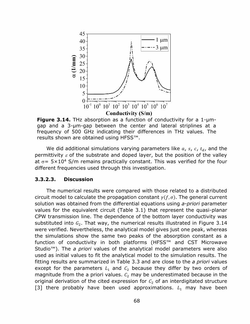
68
Figure 3.14. THz absorption as a function of conductivity for a 1-μm-
gap and a 3-μm-gap between the center and lateral striplines at a frequency of 500 GHz indicating their differences in THz values. The
results shown are obtained using HFSS™.
We did additional simulations varying parameters like 𝑎, 𝑠, 𝑐, 𝑡𝑑, and the
permittivity of the substrate and doped layer, but the position of the valley
at = 5×10⁴ S/m remains practically constant. This was verified for the four
different frequencies used through this investigation.
3.3.2.3. Discussion
The numerical results were compared with those related to a distributed
circuit model to calculate the propagation constant 𝛾(𝑓, 𝜎). The general current
solution was obtained from the differential equations using a-priori parameter
values for the equivalent circuit (Table 3.1) that represent the quasi-planar
CPW transmission line. The dependence of the bottom layer conductivity was
substituted into 𝐺2. That way, the numerical results illustrated in Figure 3.14
were verified. Nevertheless, the analytical model gives just one peak, whereas
the simulations show the same two peaks of the absorption constant as a
function of conductivity in both platforms (HFSS™ and CST Microwave
Studio™). The a priori values of the analytical model parameters were also
used as initial values to fit the analytical model to the simulation results. The
fitting results are summarized in Table 3.3 and are close to the a priori values
except for the parameters 𝐿1 and 𝐶2 because they differ by two orders of
magnitude from the a priori values. 𝐶2 may be underestimated because in the
original derivation of the cited expression for 𝐶2 of an interdigitated structure
[3] there probably have been used approximations. 𝐿1 may have been

69
underestimated because we assumed that just the distance between the two
conductors matters.
In the simulations, the absorption constant 𝛼 was extracted from the S12
parameter (Figure 3.11, both simulation programs) and from the decay of the
current-density traveling along the center stripline (Figure 3.12 and Figure
3.13, only HFSS™) and shows a significant “central valley” near 5 × 10⁴ S/m.
The results obtained by HFSS™ and CST™ were consistently similar, despite
them employing two different numerical methods. Even the various side-peaks
in the (𝛼,𝑓)–plane occur in both simulations, therefore it is unlikely that they
are artifacts. The analytical model predicts two modes (see equation (3.4)).
The first mode has a maximum of absorption whereas the absorption of the
second mode is increasing with conductivity without limit according to Figure
3.8. These second-mode absorption values are constant and proportional to
frequency for conductivity values lower than 1×10⁴ S/m, because the
transmission line acts as a low-pass filter. Beyond this conductivity value, the
second-mode absorption value increases without limit. This could be
understood by assuming that it is the CPW mode between the buried center
conductor and the outer striplines which is increasingly shortened out towards
larger values of 𝐺2. In this picture, the first mode should then be more related
to the pure microstrip mode between the two vertically separated center
conductors. For the asymmetric CPW-substitution circuit of Figure 3.6b, both
modes should then rather be linear combinations of the two Eigen-mode
solutions, the symmetric and the anti-symmetric, of a planar symmetric CPW.
However, the appearance of any second mode could not be identified from the
simulations (see Appendix E). This is probably because its absorption constant
is very high (see Figure 3.8b and Figure 3.9), so that even very close to the
input port it is too weak to be noticed. The simulation of the case of 1.0 × 10⁻¹
S/m at 1.0 × 10⁻² GHz (see Figure 3.9a), where the absorption of the second
mode should be less, did not reveal a different mode. The question then
remains as to why it exhibits that much absorption. Therefore, the analytical
model appears to be too simple to explain this unseen second mode and the
second absorption peak appearing in the plots versus conductivity.
Nevertheless, the described model fits fairly well with the first absorption peak.
From the symmetry of the replacement circuit model of Figure 3.6b, it is not
surprising that by varying 𝐺1 in the range in which previously 𝐺2 was varied,
and keeping 𝐺2 constant, produces a result similar to that of Figure 3.8. As 𝐺1
can be steered by the optical illumination of the diode structures, this effect
could be studied in the future in an optical experiment with vertically
illuminated distributed photodiodes, similar to that demonstrated previously
[91].

70
Full-wave numerical calculations of the sub-millimeter and THz losses of
a quasi-planar, coplanar waveguide (CPW) of a distributed (travelling-wave)
p-i-n-like photodiode were performed in CST™ and HFSS™ as a function of the
ground layer conductivity and frequency. Additionally, an analytical model was
implemented to validate the absorption values obtained by the simulations.
Plots of absorption versus conductivity were made in three ways. The first
method was by using equation (3.5). The second was by fitting plots of current
density versus distance with the exponential function; the argument of the
exponential function represents the absorption constant. The third approach
was by obtaining a closed-form expression for the propagation constant from
an equivalent-circuit model. The first two methods showed a local minimum in
the absorption plot around a conductivity of 5 × 10⁴ S/m. The third way, after
obtaining a priori parameter values followed for a second iteration by fitting
them with the absorption plot of the second method, showed a single peak
instead of two peaks. Despite this, the absorption values are consistently
similar to those from the first and second way, for frequencies of 500 and 2000
GHz. A possible physical reason for a second peak arising is the slow-wave
transition, where the first peak corresponds to a transition to just the electric
field being shield, while the second corresponds to a transition to the complete
electromagnetic field being shielded by the semi-conducting layer. This shows
that the equivalent-circuit model cannot be precise enough to describe the
THz-absorption behavior of the quasi-planar, coplanar waveguide (CPW) of a
distributed (travelling-wave) p-i-n-like photodiode.
According to this research the maximum possible doping value in InP of
5 × 1019 cm-3 should be on top of the second peak, thus not giving the least
possible absorption value. Doping levels higher than 5 × 1020 cm-3, equivalent
to a conductivity value of 8.0 × 10⁵ S/m and still on the second peak, are
generally not physically possible in doped semiconductors. Therefore, the
valley-value of 5 × 10⁴ S/m, corresponding to a doping of ≈ 2 × 1018 cm-3, is the
best practical conductivity value in distributed photodiode structures for THz-
applications. However, to draw more precise conclusions as to which exact
doping level to use in practice, the accurate dependence of the conductivity on
the doping level must be known for the specific semiconductor used.
3.3.3. Achievable sub-millimeter THz-power
As a continuation of the previous section, where analytical models and
simulations were performed to study the behavior of the conductivity change
of the underlying doped layer on the THz absorption, here we develop a
theoretical model describing the THz power generated from the devices
depicted in Figure 3.15. Figure 3.15 also shows two new structures (Figure
3.15b and Figure 3.15c) additional to the structure depicted in Figure 3.10.

71
These structures were simulated in HFSS with the purpose of making a
comparison in THz loss and THz power. Their dimensions are defined in Table
3.4. The analytical model for the THz power was developed taking into account
the underlying-doped-layer conductivity, the THz absorption and impedance
obtained by the RF simulations performed in Microwave CST Studio™ and
HFSS™. This chapter will start with a description of the theoretical model
employed to model the THz power originated from three different structures
defined in Figure 3.15, followed from the results and explanation of the results
obtained from this theoretical model.
Figure 3.15. The geometry for the simulations performed in CST™ and HFSS™. a) Quasi-CPW structure[70]. b) Mushroom structure. c) Wall
structure geometry.
Table 3.4: CPW parameters.
Structure a s c Mesa
thickness td
Metal
thickness t
Substrat
e
thickness ts
(m) (m) (m) (m) (m) (m)
Quasi CPW Structure 4 1 10 1 0.1 200 Mushroom-CPW
Structure 4 1 10 1 0.1 500
Wall-CPW Structure
[70] 4 1 10 1 6 500
Figure 3.16 shows a VI-TW-UTC photomixer, where the transmission line
(CPW) and its antenna is clearly depicted. This picture shows the axis
coordinates, where the z axis is parallel to the CPW, and the y axis is
perpendicular to the photomixer surface. The origin of this system coordinates
is located at the intersection between the backward wave attenuator and the

72
CPW. This transmission line has a length L. The antenna is located at position
L. The antenna of this device is similar to a slot bow tie, but with transmission
lines substituting all edges. The motivation to do this is to allow laser
illumination (on the left side) to enter from above into the chip (with a
reflection at a Bragg-reflector at the bottom of the chip, to be focused onto
the waveguide from below). From symmetry reasons for the antenna the same
is introduced also on the right side.
Figure 3.16. Transmission line geometry used in the computation of the achievable THz power. This is a micrograph of the fabricated mixers in the
stage before the air-bridge is fabricated which connects the top of the mesa diode structure with the right side of the antenna.
The THz power generated at the position of the antenna of a vertically
illuminated traveling-wave photomixer is given by:
𝑃𝑇𝐻𝑧(𝜔) =1
2𝑍 ∙ |𝐼𝑝ℎ,𝑎𝑛𝑡(𝜔)|
2 (3.6)
where
𝐼𝑝ℎ,𝑎𝑛𝑡(𝜔) =𝐼𝑝ℎ,𝑎𝑛𝑡(0)
1 + 𝑖𝜔𝜏𝑡𝑟 (3.7)
is the peak-value of the modulation part at angular frequency 𝜔 = 𝜔2-𝜔1 of the
photocurrent obtained by the beat of the two lasers (see section 1.2.1). Its
theoretical maximum at 𝜔 → 0 is:
𝐼𝑝ℎ,𝑎𝑛𝑡(0) = 2ℜ(0)√𝑃𝑁𝐼𝑅1 ∙ 𝑃𝑁𝐼𝑅2 = ℜ(0)𝑃𝑁𝐼𝑅,𝑡𝑜𝑡
=𝜂𝑒
ℎ𝜈(1 − 𝑅)(1 − 𝑒−𝛼𝐿)𝑃𝑁𝐼𝑅,𝑡𝑜𝑡
(3.8)
as the maximum THz-power is obtained at 𝑃𝑁𝐼𝑅1 = 𝑃𝑁𝐼𝑅2 = 0.5𝑃𝑁𝐼𝑅,𝑡𝑜𝑡. 𝜂 is the
quantum-efficiency, which is given mainly by the photoconductive gain, 𝐺 ≤
𝜏𝑟𝑒𝑐 𝜏𝑡𝑟⁄ . The responsivity ℜ was simulated in Synopsis TCAD. Details about
these simulations are explained in chapter 2. The total responsivity for a 3 µm
diameter UTC-PD was found to be ℜ ≈ 0.2 A/W (see Figure 2.3), and

73
experimentally observed by us on a 5-µm-diameter UTC PD (focus from a with
4mm-diameter illumination of an aspheric lens with f=6.25mm) to be 0.05
A/W at 𝑉𝑏 = −1.6 V, while the quantum limit is ℜ𝑚𝑎𝑥(1.5μ𝑚) ≈ 1.25 A/W.
𝜏𝑡𝑟 is the transit time between the doped absorption layer and the highly
doped “sub-collector” bottom layer as shown in Figure 3.15 (a, b, or c), Iph is
the total photocurrent, Z is the characteristic transmission line impedance
(ideally matched to the antenna impedance). 𝜏𝑡𝑟 is calculated as 𝜏𝑡𝑟 = 𝑡𝑑/𝑣𝑒,
where td is the mesa thickness, as shown in Figure 3.15 and listed in Table 3.5,
ve is the electron velocity which can be as high as the overshoot velocity, which
is ve=4×107 cm/s in InGaAs. Therefore, = 2.5 ps, whose value corresponds to
𝑓𝑚 = 1/(2π𝜏𝑡𝑟) = 64 GHz.
The total photocurrent superimposed at the antenna (at location 𝑧 = 𝐿)
from all contributions along the transmission line shown in Figure 3.16 is
calculated as the convolution of the total photocurrent at:
𝐼𝑝ℎ,𝑎𝑛𝑡(𝜔) = ∫ 𝑖(𝜔, 𝑧)𝑒−𝛾𝑇𝐻𝑧(𝜔)∙(𝐿−𝑧)𝐿
0
𝑑𝑧 (3.9)
where 𝛾𝑇𝐻𝑧 ≔ 𝛼𝑇𝐻𝑧 + 𝑗𝛽𝑇𝐻𝑧 is the propagation constant defined in section
3.3.2.1, 𝑖( 𝜔, 𝑧) is the incremental part of the photocurrent generated over an
interval Δ𝑧 at the position z. In equation (3.9) the propagation phase delay on
the transmission line is modeled as 𝑒−𝛾𝑇𝐻𝑧(𝜔)∙𝑧.
To realize phase matching, i.e. the coincident arrival of all the partial
current waves at the foot-point of the antenna, the additional phase shift to
impose on the incremental photocurrents should be 𝑖(𝜔, 𝑧) = |𝑖(𝜔, 𝑧)| ∙ 𝑒−𝑗𝛽𝑇𝐻𝑧∙𝑧.
This phase cancels the phase in eq. (3.9), so that one can leave out the
imaginary part of the exponential term (the “phasor”) and set 𝛾𝑇𝐻𝑧 to be just
𝛼𝑇𝐻𝑧. This phase-match (Δ𝑘 = 0 between the optical fringes and the submm-
signal propagation) is obtained from the angle tuning between the two laser
beams as described in section 1.2.3.1.1 and is fulfilled if 𝑣𝑜𝑝𝑡 = 𝑣𝑇𝐻𝑧, where 𝑣𝑜𝑝𝑡
is the velocity of the interference fringes along the surface, and 𝑣𝑇𝐻𝑧 is the
group velocity of a THz wave generated in a dispersionless transmission line
[7]. The attenuation 𝛼𝑇𝐻𝑧 is obtained from the simulations done in CST
Microwave Studio™ y HFSS™ as explained in section 3.3.2.2.2.
Using with the conductivity, the total photocurrent over the stripline is
𝐼(𝜔) = 𝑉𝑏 ∙ 𝐺𝑇𝑂𝑇𝐴𝐿(𝜔) (3.10)
and the incremental part of it over an interval 𝛥𝑧, 𝑖(𝑧, 𝜔), is computed as:

74
𝑖( 𝜔, 𝑧) = 𝑉𝑏 ∙ 𝑔𝑇𝑂𝑇𝐴𝐿(𝜔, 𝑧) (3.11)
where 𝐺𝑇𝑂𝑇𝐴𝐿(𝜔) would be equal to 𝑔𝑇𝑂𝑇𝐴𝐿(𝜔, 𝑧) ∙ 𝐿 in case of uniform illumination.
But as there is an illumination profile, the following considerations should be
taken into account. 𝑉𝑏 is the applied voltage, 𝑔𝑇𝑂𝑇𝐴𝐿(𝜔, 𝑧) is the conductivity
modulated by the illumination. The modulated conductivity due to the optical
illumination results from two resistances in series. Written in conductances per
length:
𝑔𝑇𝑂𝑇𝐴𝐿 =𝑔𝑝ℎ ∙ 𝑔0
𝑔𝑝ℎ + 𝑔0 (3.12)
where 𝑔𝑝ℎ is the length-specific conductance due to the optical illumination in
the absorption layer, and 𝑔0 is the intrinsic conductance due to the doped
bottom layer. The intrinsic conductivity due to the effective current cross
section of the doped layer is approximately
𝑔0 = 2 ∙ 𝜎 ∙𝐴𝑒𝑓𝑓
𝑠 𝐿= 2𝜎
𝛿
𝑠 (3.13)
where 𝑠 ≈ (𝑏 + 𝑐)/2 is the effective distance traveled by the electrons between
the lateral two (therefore the factor of 2) striplines and the center stripline of
the devices shown in Figure 3.15, and their values are listed in table Table 3.4.
𝐴𝑒𝑓𝑓 is approximated as 𝐴𝑒𝑓𝑓 = 𝛿 ∙ 𝐿, where 𝛿 is the doped layer thickness. 𝜎 is
the conductivity of the bottom layer.
The incremental THz photocurrent per length generated at the position z
of a vertically illuminated traveling-wave photomixer is given by:
|𝑖𝑝ℎ(𝑃, 𝜔, 𝑧)| ≔𝑑𝐼𝑝ℎ(𝑃, 𝜔, 𝑧)
𝑑𝑧= ℜ(𝜔) ∙ 𝑝(𝑃, 𝑧) (3.14)
where
𝑝(𝑃, 𝑧) =𝑃
√𝜋𝑤𝑁𝐼𝑅
∙ exp (−(𝑧−𝑧0
𝑤𝑁𝐼𝑅)2
) (3.15)
is the astigmatic Gaussian beam illumination one-dimensional intensity
distribution along the transmission line whose maximum is located at z0,
expressed in [W/m], the other direction is integrated over the lateral
dimension of the central stripline mesa structure. ℜ is the responsivity related
to the vertical mesa-structure explained and simulated in section 1.2, which is
now here in series with the doped bottom layer. 𝑃 is the total optical power.
The (two-dimensional) photocurrent density is obtained from equation (3.14),
by dividing it through the central stripline width, 𝑎,

75
|𝐽𝑝ℎ(𝑧)| =|𝑖𝑝ℎ(𝑧)|
𝑎≔
1
𝑎
𝑑𝐼𝑝ℎ
𝑑𝑧= ℜ ∙
𝑝(𝑧)
𝑎= ℜ ∙
𝑑𝑃
𝑑𝐴 (3.16)
The total photocurrent of a LE-device would be
𝐼𝑝ℎ = 𝐽𝑝ℎ ∙𝜋
4𝐷2 = ℜ𝐿𝐸 ∙ 𝑃 (3.17)
From the TCAD simulations of a cylindrical device of diameter 𝐷 = 3 m
(without a bottom layer which connects to a sideward metal electrode!) the
lumped-element responsivity ℜ𝐿𝐸 was obtained to be 0.2 A/W under 2V of
reverse bias and an optical input power of 1.8 × 10⁻⁴ W. We assume here that
a TW-device of 4 m central stripline (mesa) width would have a similar
responsivity per area. However, note that simulations for a 𝐷 = 10 m device
gave a slightly higher responsivity, see Figure 2.2, although the optical power
was confined to the devices (no radiation spill-over in the simulation).
Therefore, we estimate that the TW responsivity ℜ would be similar,
though somewhat higher. Under the simplifying assumption that ℜ: = ℜ/𝑉𝑏 is
a constant, which would be 0.025 A/WV at -2V, we obtain
𝐺𝑝ℎ(𝑃, 𝜔) = ℜ(𝜔) ∙ 𝑃 (3.18)
𝑔𝑝ℎ(𝑃, 𝜔, 𝑧) = ℜ(𝜔) ∙ 𝑝(𝑃, 𝑧) (3.19)
using eq. (3.12),
𝑔𝑡𝑜𝑡𝑎𝑙(𝑃, 𝜔, 𝑧) =
ℜ(𝜔) ∙ 𝑝(𝑃, 𝑧)
1 +ℜ(𝜔)𝑔0
∙ 𝑝(𝑃, 𝑧)
(3.20)
This represents also the modulation amplitude, since the dark conductivity
is zero. In case of 𝑃 → ∞ we have 𝑔𝑡𝑜𝑡𝑎𝑙(𝑃, 𝜔, 𝑧) → 𝑔0, so that a saturated output
power limit is given. The NIR input saturation power is then 𝑃𝑠𝑎𝑡(𝑃, 𝜔) =
𝑔0/ℜ(𝜔). Note that this infrared power level might be beyond the thermal
damage threshold we observe (13mA/250mW for a 5-µm diameter LE device).
The THz-power is now given from eq. (3.6), using eq. (3.20) and (3.15),
𝑃𝑇𝐻𝑧 =𝑍
2[Δ𝐼𝑝ℎ,𝑎𝑛𝑡(𝑃, 𝜔)]
2=
𝑍
2[∫ 𝑔𝑡𝑜𝑡𝑎𝑙(𝑃, 𝜔, 𝑧)𝑑𝑧
𝐿
0
∙ 𝑉𝑏]
2
(3.21)
The values used in this research are described in Table 3.5.

76
Table 3.5. Parameter values used (𝐷 is the cylindrical diameter used in TCAD
simulations).
Symbol Value Units
Lumped element device in the TCAD simulations
Applied voltage 𝑉𝑏 2 V
Responsivity ℜ 2.9 × 10⁻² A/W
Optical Power 𝑃 2.5 × 10⁻¹ W
Device area (𝐷 = 3 𝜇𝑚) 𝐴 = 4𝜋(𝐷 2⁄ )2 1.8 × 10⁻¹² m2
Device area (𝐷 = 10 𝜇𝑚) 𝐴 = 4𝜋(𝐷 2⁄ )2 2.0 × 10⁻¹¹ m2
TW device
Length 𝐿 3 × 10⁻⁴ m
illumination waist 𝑤𝑁𝐼𝑅 1 × 10⁻⁴ m
The steps used to obtain the THz power are as follows. First, the
impedance Z is obtained through the procedure used in section 3.3.1 for the
structures depicted in Figure 3.15. A responsivity value ℜ ≈ 0.2 A/W and optical
power of 2.1 × 10⁻² W were used. This value was chosen because this is the
optical input power before the responsivity falls abruptly for the 3-m diameter
device (see Figure 2.3). The next step is to plot 𝑃𝑇𝐻𝑧(𝑧, 𝜔) vs 𝑧0 through
equation (3.9) to obtain the value of 𝑧0 where 𝐼𝑝ℎ,𝑎𝑛𝑡(𝑧, 𝜔) is maximum. This 𝑧0
value is used to compute 𝑃𝑇𝐻𝑧(𝑧, 𝜔) again, which will be used to obtain the THz
power from equation (3.21).
Figure 3.17a shows the Gaussian beam pattern 𝑝(𝑃, 𝑧) used to excite the
devices of Figure 3.15. The Gaussian beam has a maximum of 120 W/m,
computed with a power of 2.1 × 10⁻² W, which corresponds to a responsivity of
0.2 A/W, according to the results for the 3-m diameter device shown in Figure
2.3. Before showing the results, an optimization should be carried, and this is
the position 𝑧0 where the terahertz power is maximum. Figure 3.17b shows
the photocurrent as a function of the position 𝑧0. The maximum terahertz
power occurs at 𝑧0 = 3 × 10⁻⁴ m. The underlying-doped layer conductivity was
also varied. For all the conductivities, the position 𝑧0 where the terahertz
power is maximum were the same. Therefore, the value 𝑧0 = 3 × 10⁻⁴ m will be
used for all the computation. Figure 3.17c and Figure 3.17d show the terahertz
power 𝑃𝑇𝐻𝑧(𝜎, 𝑓) as a function of the underlying-doped layer conductivity and
frequency, respectively.

77
Figure 3.11a shows the absorption versus conductivity for the Quasi-CPW
structure. As was stated earlier, there is a valley where a minimum of
absorption exist. Figure 3.18 shows the plots of THz absorption vs doped layer
conductivity for the Wall-CPW and Mushroom-CPW structures (see Figure
3.15) at frequencies of 500, 1000, 1500, and 2000 GHz. These plots were
obtained using the procedure described in section 3.3.2.2 with the HFSS™
software. Different from the THz absorption in the Quasi-CPW structure, the
minimum of the absorption valley is not clearly defined.
a) b)
c) d) Figure 3.17. a) Gaussian Beam pattern 𝑝(𝑧) from equation (3.15). b)
Photocurrent 𝐼𝑝ℎ,𝑎𝑛𝑡 obtained from equation (3.9) as a function of the
Gaussian beam maximum position 𝑧0. c) Plot of terahertz power versus the
underlying-doped layer conductivity at 500 GHz. d) Plot of terahertz power
vs frequency with the doped layer at a conductivity of 4.5 × 10⁷ S/m.

78
a)
10-1
100
101
102
103
104
105
106
107
108
0
1x10⁴
2x10⁴
3x10⁴
4x10⁴
5x10⁴
TH
z A
bsorp
tion (
m-1)
Conductivity (S-1)
500 GHz
1000 GHz
1500 GHz
2000 GHz
Wall CPW
b)
10-1
100
101
102
103
104
105
106
107
108
0
1x10⁴
2x10⁴
3x10⁴
4x10⁴
5x10⁴
TH
z A
bso
rpti
on (
m-1
)
Conductivity (S-1
)
500 GHz
1000 GHz
1500 GHz
2000 GHz
Mushroom CPW
Figure 3.18. THz absorption as a function conductivity for the Wall-CPW
(left), and Mushroom-CPW (right) structures.
Figure 3.19 shows the THz power vs the doped-layer conductivity with
both axes in logarithmic scale, values for 500, 1000, 1500, and 2000 GHz and
for all the three devices specified in Figure 3.15. The THz power increases as
the n-layer conductivity increases for all the three devices. This figure also
shows an approximately linear log-log plot with small deviations from this
behavior. These deviations suggest the influence of the THz absorption in the
THz power by the three devices. Figure 3.20 shows double-axis plots, in which
the left axis is the THz absorption and the right axis is the THz absorption. The
maximum deviations from the approximately linear log-log behavior appears
to happen when the THz absorption is maximum in both peaks as shown in
Figure 3.20, for the QCPW device. These deviations are also shown in Figure
3.20b y Figure 3.20c, which instead of two deviations as the case of the QCPW

79
device, appears to be one clearly defined on a small n-layer conductivity
interval. Figure 3.19 also shows the decreasing nature of the THz power as the
frequency increases from 500 to 2000 GHz. This decreasing nature of the THz
Power with the frequency is observed also in Figure 3.21. Figure 3.21 shows
the behavior of the THz power vs the frequency for conductivities of 1.0 × 10⁻¹,
2.1 × 10³, 5.0 × 10⁴, 5.8 × 10⁵, and 4.5 × 10⁷ S/m.

80
a)
b)
c)
Figure 3.19. Curves of THz Vs doped-layer conductivity for 500, 1000, 1500 and 2000 GHz for a) Quasi-CPW structure, b) Wall-CPW structure,
and c) Mushroom-CPW structure.

81
a)
b)
c)
Figure 3.20. Curves of double axis showing the THz absorption (left axis)
and THz absorption (right axis) Vs doped-layer conductivity for 500, 1000, 1500 and 2000 GHz for a) Quasi-CPW structure, b) Wall-CPW structure,
and c) Mushroom-CPW structure.

82
a)
b)
c)
Figure 3.21. Curves of THz Power vs frequency for five doped-layer conductivities for a) Quasi-CPW structure, b) Wall-CPW structure, and c)
Mushroom-CPW structure.

83
Figure 3.22 shows the behavior of the THz power vs the frequency for
conductivities of 1.0 × 10⁻¹, 2.1 × 10³, 5.0 × 10⁴, 5.8 × 10⁵, and 4.5 × 10⁷ S/m by
making a comparison between the three devices defined in Figure 3.15. The
comparison between the three devices with the n-layer conductivity of 1.0 ×
10−1 and 4.5 × 10⁷ S/m, which correspond with the ideal cases of microstrip line
and CPW (see Figure 3.5), shows that the Quasi CPW device have a higher
output THz power than the Wall- and Mushroom-CPW devices. The Mushroom-
CPW device also has a higher output power than the Wall-CPW device. This is
explained using Figure 3.23. This picture shows that for all the n-
conductivities, the Quasi-CPW characteristic impedance is always higher than
the Mushroom-CPW and Wall-CPW characteristic impedance; the Mushroom-
CPW characteristic impedance is also higher than the Wall-CPW characteristic
impedance. The advantages of higher THz output power for any of the three
devices is not clear with the n-layer conductivities of 2.1 × 10³, 5.0 × 10⁴ and,
5.8 × 10⁵.

84
a) b)
c) d)
e)
Figure 3.22. Curves of photocurrent vs frequency for Quasi-CPW, Wall-CPW, and Mushroom-CPW devices for the following n-layer conductivities a) 1.0 × 10⁻¹,
b) 2.1 × 10³, c) 5.0 × 10⁴, d) 5.8 × 10⁵ and, e) 4.5 × 10⁷ S/m.

85
Figure 3.23. Plot of impedance vs the underlying layer conductivity
Therefore, the main way to reach reasonable THz power at the antenna
position according to the above described model is by increasing the n-layer
conductivity. Note that other than suspected from the beginning, the effect of
the THz absorption shown in Figure 3.18 is not appreciable.
Geometries in which a metal layer replaces the semiconductor layer
should lead, according to Figure 3.21, to a significant increase in output power.
Unfortunately, conventional microfabrication architectures exclude this. Flip-
chip techniques should be the way to introduce a metal bottom layer, but those
techniques are extremely complicated and unreliable. Though, a metal-
semiconductor-metal sandwich structure is not to be illuminated anymore
vertically, so that then only edge-illuminated designs would make sense.
Note that the finding that the influence of the conductivity on the output
power is stronger through the responsivity than through the waveguide
absorption, is also very relevant for the discussion of the output power of
lumped-element devices. Similarly, here designs with a bottom electrode from
metals instead from highly-doped semiconductors should also then bring a
breakthrough in output power.
The structures depicted in Figure 3.13b and Figure 3.13c, which are the
Mushroom-CPW and Wall-CPW structure respectively, are characterized by a
lower characteristic impedance, as showed in Figure 3.19. Therefore, despite
they modify the distributed parameters, they do not contribute significantly in
THz output power. Additionally, equation (3.22) marks the way to improve the
THz output power: The research of high-impedance characteristic transmission
lines.

86
4. Conclusions
4.1. Discussion
To reach our goal of performing simulations to analyze and design of VI
TW UTC photomixers the following simulations areas were done:
Semiconductor Carrier Transport and High-Frequency and Electromagnetic
simulations.
DC carrier transport were done using the Hydrodynamic Carrier Transport
Model with the aid of the numerical simulator Sentaurus TCAD. For this study,
a cylindrical UTC photodiode of 3-m diameter LE UTC device was studied. The
physical behavior of the LE-UTC device was investigated at both low and high
light levels. Under high light levels, the electrons start to accumulate at the
cliff layers due to the discontinuities present at the cliff layers in the energy
bandgap structure. Under this situation, the space charge effect become
strong reducing the linearity of the LE-UTC devices and maximum output
power. This suggest also the way in which the LE-UTC devices can be
improved by the change of the material of the absorption layer from InGaAs
to GaAsSb. This makes the junction between the absorption and collection
layer a heterojunction type 2, by which the conduction and valence band
energies from the absorption layer are higher than the energies from the
collection layer. This allows a smooth transition for the carrier transport
between these layers. The 3-m diameter LE UTC device showed a maximum
responsivity of 0.2 A/W. A velocity overshoot of 4 × 107 cm/s was obtained at
the absorption layer. A maximum electron temperature of 7000 K was
obtained at the collection layer. Despite the electron velocity is maximum at
the absorption layer, the highest electron temperature is due to the intervalley
scattering present at the collection layer and strong electric field. Finally, due
to the complex carrier transport, several planned simulations were not
successful carried out.
Full-wave numerical calculations of the sub-millimeter and THz losses of
a quasi-planar, coplanar waveguide (CPW) of a distributed (travelling-wave)
p-i-n-like photodiode were performed in CST™ and HFSS™ as a function of the
ground layer conductivity and frequency. Additionally, an analytical model was
implemented to validate the absorption values obtained by the simulations.
Plots of absorption versus conductivity were made in three ways. The first
method was by using equation (3.5). The second was by fitting plots of current
density versus distance with the exponential function; the argument of the
exponential function represents the absorption constant. The third approach
was by obtaining a closed-form expression for the propagation constant from

87
an equivalent-circuit model. The first two methods showed a local minimum in
the absorption plot around a conductivity of 5 × 10⁴ S/m. The third way, after
obtaining a priori parameter values followed for a second iteration by fitting
them with the absorption plot of the second method, showed a single peak
instead of two peaks. Despite this, the absorption values are consistently
similar to those from the first and second way, for frequencies of 500 and 2000
GHz. A possible physical reason for a second peak arising is the slow-wave
transition, where the first peak corresponds to a transition to just the electric
field being shield, while the second corresponds to a transition to the complete
electromagnetic field being shielded by the semi-conducting layer. This shows
that the equivalent-circuit model cannot be precise enough to describe the
THz-absorption behavior of the quasi-planar, coplanar waveguide (CPW) of a
distributed (travelling-wave) p-i-n-like photodiode.
According to this research the maximum possible doping value in InP of
5 × 1019 cm-3 should be on top of the second peak, thus not giving the least
possible absorption value. Doping levels higher than 5 × 1020 cm-3, equivalent
to a conductivity value of 8.0 × 10⁵ S/m and still on the second peak, are
generally not physically possible in doped semiconductors. Therefore, the
valley-value of 5 × 10⁴ S/m, corresponding to a doping of ≈ 2 × 1018 cm-3, is the
best practical conductivity value in distributed photodiode structures for THz-
applications. However, to draw more precise conclusions as to which exact
doping level to use in practice, the accurate dependence of the conductivity on
the doping level must be known for the specific semiconductor used.
An analytical model to account the THz output generated by three type of
devices, Quasi-CPW, Wall-CPW, and Mushroom-CPW devices was developed
at the input of the photomixer antenna. This analytical model takes into
account the optical responsivity measured through the photocurrent delivered
by the hydrodynamic carrier transport simulation, the characteristic
impedance, the optical input power, the operating frequency, the n-layer
doping (measured indirectly through the conductivity). This analytical model
showed an increasing terahertz output power as the n-layer conductivity
increases. The maximum THz output power is reached when the n-layer is
replaced by a metal, but at the current state of the art, the conventional
microfabrication excludes this possibility.
4.2. Future Work
The simulations based in carrier transport modeling and high-frequency
RF simulations have proved to be of great help in the understanding of the
physical functioning of VI-TW-UTC-PD devices. As a continuation of this
project, several further steps can be taken.

88
One step is the simulation of UTC-PD devices in which the transition
between the collection and absorption layer uses a junction of the type
homojunction to study the performance in which the cliff layers are suppressed
and, consequently, the transition between the collection and absorption layer
is smooth.
A second step, simulations using the Silvaco TCAD tools are proposed to
understand the differences with Synopsys Sentaurus TCAD.
The third step was a consequence that more different semiconductor
analysis was needed and were not possible to develop in this thesis. These are
mixed simulations like AC analysis, small-signal analysis and, transient
response analysis.
The fourth step comes from the fact that the VI-TW-UTC-PD device is a
transmission line based in UTC-PD device, it is known that both kind of
simulations are needed to develop knowledge of performance. This doctoral
thesis developed both simulations separately. The next step will be the
integration between the semiconductor modeling and high-frequency RF
simulations by use of the tools like Comsol Multiphysics. The software not only
allows to simulate both types of physical phenomena, but also other
phenomena such as optical and thermal simulations. Therefore, a future work
will include the simulations of the vertical illumination by the two lasers and
the simulation of the optical lenses needed to elaborate the photomixer
experiment. The last version of Comsol (5.2a, year 2016) only supports the
Drift-Diffusion Carrier Transport Model. Therefore, the integration with carrier
transport modeling will be limited to the Drift-Diffusion Model. Other ways to
integrate the different physical phenomena will be the use of programming
tools like Visual Studio (C++, C#, Visual Basic, Java), Matlab, and Python.
The fifth step comes from analyzing equation (1.9), which shows that one
way to improve the THz-power output is by increasing the antenna resistance.
But, to increase the antenna resistance it is needed to develop new high-
frequency structures for the transmission line that have a high characteristic
impedance value assuming that this is perfectly coupled to the VI-TW-UTC-PD
device. As they are developed, the behavior of the absorption versus the n-
layer conductivity is proposed as part of the study to understand the
performance of these new structures.

89
5. Bibliography
[1] E. R. Brown, K. A. McIntosh, F. W. Smith, M. J. Manfra, and C. L. Dennis, “Measurements of optical-heterodyne conversion in low-temperature-grown GaAs,” Appl. Phys. Lett., vol. 62, no. 11, pp. 1206–1208, Mar.
1993.
[2] E. R. Brown, K. a. McIntosh, F. W. Smith, K. B. Nichols, M. J. Manfra, C. L. Dennis, and J. P. Mattia, “Milliwatt output levels and superquadratic
bias dependence in a low-temperature-grown GaAs photomixer,” Appl. Phys. Lett., vol. 64, no. 24, p. 3311, 1994.
[3] E. Brown, K. McIntosh, K. Nichols, and C. L. Dennis, “Photomixing up to 3.8 THz in low-temperature-grown GaAs,” Appl. Phys. Lett., vol. 66, no.
3, pp. 285–287, 1995.
[4] K. a. McIntosh, E. R. Brown, K. B. Nichols, O. B. McMahon, W. F. DiNatale,
and T. M. Lyszczarz, “Terahertz photomixing with diode lasers in low-temperature-grown GaAs,” Appl. Phys. Lett., vol. 67, no. 26, p. 3844,
1995.
[5] S. Verghese, K. a. K. A. McIntosh, and E. R. Brown, “Optical and terahertz
power limits in the low-temperature-grown GaAs photomixers,” Appl. Phys. Lett., vol. 71, no. 19, pp. 2743–2745, 1997.
[6] S. Verghese, E. Duerr, K. McIntosh, and SM, “A photomixer local
oscillator for a 630-GHz heterodyne receiver,” IEEE Microw. Guid. Wave Lett., vol. 9, no. 6, pp. 245–247, 1999.
[7] S. Matsuura, G. a. Blake, R. A. Wyss, J. c. C. Pearson, C. Kadow, A. W. Jackson, and A. C. Gossard, “A traveling-wave THz photomixer based on
angle-tuned phase matching,” Appl. Phys. Lett., vol. 74, no. 19, p. 2872, 1999.
[8] S. Duffy, S. Verghese, A. McIntosh, and A, “Accurate modeling of dual dipole and slot elements used with photomixers for coherent terahertz
output power,” IEEE Trans. Microw. Theory Tech., vol. 49, no. 6, pp. 1032–1038, 2001.
[9] K. Giboney, J. Rodwell, and JE, “Traveling-wave photodetector theory,” IEEE Trans. Microw. Theory Tech., vol. 45, no. 8, pp. 1310–1319, 1997.
[10] K. S. K. Giboney, M. J. W. M. Rodwell, and J. J. E. Bowers, “Traveling-wave photodetector design and measurements,” IEEE J. Sel. Top.
Quantum Electron., vol. 2, no. 3, pp. 622–629, 1996.
[11] D. Saeedkia, “Modeling and design of photoconductive and

90
superconductive terahertz photomixer sources,” University of Waterloo,
2005.
[12] A. W. M. Lee, Q. Qin, S. Kumar, B. S. Williams, Q. Hu, and J. L. Reno, “Real-time terahertz imaging over a standoff distance (>25 meters),”
Appl. Phys. Lett., vol. 89, no. 14, p. 141125, 2006.
[13] J. Danielson, Y.-S. Lee, J. Prineas, J. Steiner, M. Kira, and S. Koch,
“Interaction of Strong Single-Cycle Terahertz Pulses with Semiconductor Quantum Wells,” Phys. Rev. Lett., vol. 99, no. 23, Dec. 2007.
[14] N. Shimizu, N. Watanabe, T. Furuta, and T. Ishibashi, “Improved Response of Uni-Traveling-Carrier Photodiodes by Carrier Injection,” Jpn.
J. Appl. Phys., vol. 37, pp. 1424–1426, 1998.
[15] H. Ito, T. Furuta, F. Nakajima, K. Yoshino, and T. Ishibashi, “Photonic
generation of continuous THz wave using uni-traveling-carrier photodiode,” J. Light. Technol., vol. 23, no. 12, pp. 4016–4021, Dec.
2005.
[16] G. Torrese, I. Huynen, J. Raskin, and A. Vander Vorst, “Analysis and
Design of pin Traveling-Wave Photodetectors for High Power and Wide-
Bandwidth Applications,” IEEE Trans. Microw. Theory Tech., vol. 29, no. 11, pp. 1174–1182, 1981.
[17] S. Kodama and H. Ito, “UTC-PD-Based Optoelectronic Components for High-Frequency and High-Speed Applications,” IEICE Trans. Electron.,
vol. E90–C, no. 2, pp. 429–435, Feb. 2007.
[18] K. Sakai, Terahertz optoelectronics. Heidelberg: Springer, 2005.
[19] T. G. Phillips, “Submillimeter astronomy (heterodyne spectroscopy),” Proc. IEEE, vol. 80, no. 11, pp. 1662–1678, 1992.
[20] P. H. Siegel, “Terahertz Technology in Biology and Medicine,” IEEE Trans. Microw. Theory Tech., vol. 29, no. 6, pp. 575–2447, Oct. 2004.
[21] A. Fitzgerald, E. Pickwell, V. Wallace, A. Purushotham, S. Pinder, M. Linan, R. Pye, and T. Ha, “Medical Applications of Broadband Terahertz
Pulsed Radiation,” in Lasers and Electro-Optics Society, 2005. LEOS 2005. The 18th Annual Meeting of the IEEE, 2005, vol. 3, pp. 103–104.
[22] E. Peytavit, S. Arscott, D. Lippens, G. Mouret, S. Matton, P. Masselin, R.
Bocquet, J. F. Lampin, L. Desplanque, and F. Mollot, “Terahertz frequency difference from vertically integrated low-temperature-grown GaAs
photodetector,” Appl. Phys. Lett., vol. 81, no. 7, p. 1174, 2002.
[23] T. Ishibashi, S. Kodama, N. Shimizu, and T. Furuta, “High-speed

91
response of uni-traveling-carrier photodiodes,” Jpn. J. Appl. Phys., vol.
36, no. 10, pp. 6263–6268, 1997.
[24] N. Shimizu, Y. Muramoto, Y. Miyamoto, and T. Ishibashi, “High speed InP/InGaAs uni-traveling-carrier photodiodes,” Conf. Proceedings. 2000
Int. Conf. Indium Phosphide Relat. Mater. (Cat. No.00CH37107), pp. 313–316, 2000.
[25] T. Noguchi, A. Ueda, H. Iwashita, S. Takano, Y. Sekimoto, M. Ishiguro, T. Ishibashi, H. Ito, and T. Nagatsuma, “Millimeter wave generation using
a uni-traveling-carrier photodiode,” in 12th Int. Space Terahertz. Technol. Symp., San Diego, CA, 2001.
[26] J. Liu, Photonic devices, First. New York: Cambridge University Press, 2005.
[27] K. S. Giboney, M. J. W. Rodwell, and J. E. Bowers, “Traveling-wave photodetectors,” IEEE Photonics Technol. Lett., vol. 4, no. 12, pp. 1363–
1365, 1992.
[28] V. M. Hietala, G. a. Vawter, T. M. Brennan, and B. E. Hammons,
“Traveling-wave photodetectors for high-power, large-bandwidth
applications,” IEEE Trans. Microw. Theory Tech., vol. 43, no. 9, pp. 2291–2298, 1995.
[29] D. Lasaosa, J. Shi, D. Pasquariello, K.-G. Gan, M.-C. Tien, H.-H. Chang, S.-W. Chu, C.-K. Sun, Y.-J. Chiu, and J. E. Bowers, “Traveling-wave
photodetectors with high power-bandwidth and gain-bandwidth product performance,” IEEE J. Sel. Top. Quantum Electron., vol. 10, no. 4, pp.
728–741, 2004.
[30] C. Barrientos Z, V. Calle, M. Diaz, F. P. Mena, J. Vukusic, J. Stake, and
E. a Michael, “Vertically illuminated TW-UTC photodiodes for terahertz generation,” in Proceedings of SPIE, 2012, vol. 8452, no. 1, p. 84522I–
84522I–11.
[31] J. E. Giboney, K.S.; Rodwell, Mark J W; Bowers, “Traveling-wave
photodetector,” IEEE Photonics Technol. Lett., vol. 4, no. 12, pp. 1363–1365, Jul. 1992.
[32] J. E. Bowers and C. A. Burrus, “High-speed zero-bias waveguide
photodetectors,” Electronics Letters, vol. 22, no. 17. p. 905, 1986.
[33] K. S. K. Giboney, R. L. Nagarajan, T. T. E. Reynolds, S. T. S. Allen, R. R.
P. Mirin, M. J. W. M. Rodwell, J. E. J. Bowers, and R. Ngarajan, “Travelling-wave photodetectors with 172-GHz bandwidth and 76-GHz
bandwidth-efficiency product,” IEEE Photonics Technol. Lett., vol. 7, no.

92
4, pp. 412–414, Apr. 1995.
[34] E. A. Michael, “Travelling-wave photonic mixers for increased continuous-
wave power beyond 1 THz,” Semicond. Sci. Technol., vol. 20, no. 7, pp. S164–S177, Jul. 2005.
[35] H. R. Khazaei, O. Berolo, R. James, W. J. Wang, P. Maigné, M. Young, K. Ozard, M. Reeves, and F. M. Ghannouchi, “Charge carrier effect on the
microwave losses observed on traveling-wave electrodes used in electro-optic modulators,” Microw. Opt. Technol. Lett., vol. 17, no. 4, pp. 236–
241, 1998.
[36] T. Ishibashi, N. Shimizu, S. Kodama, H. Ito, T. Nagatsuma, and T. Furuta,
“Uni-Traveling-Carrier Photodiodes - OSA Trends in Optics and Photonics Series,” in Ultrafast Electronics and Optoelectronics, 1997, vol. 13, pp.
83–87.
[37] D. Pasalic and R. Vahldieck, “A hybrid drift-diffusion-TLM analysis of
traveling-wave photodetectors,” IEEE Trans. Microw. Theory Tech., vol. 53, no. 9, pp. 2700–2706, Sep. 2005.
[38] Y. Hirota, T. Hirono, T. Ishibashi, and H. Ito, “Traveling-wave
photodetector for 1.55 um wavelength fabricated with unitraveling-carrier photodiodes,” Appl. Phys. Lett., vol. 78, no. 24, pp. 3767–3769,
2001.
[39] E. Rouvalis, C. C. Renaud, D. G. Moodie, M. J. Robertson, and A. J. Seeds,
“Continuous wave terahertz generation from ultra-fast InP-based photodiodes,” IEEE Trans. Microw. Theory Tech., vol. 60, no. 3, pp. 509–
517, 2012.
[40] E. A. Michael, B. Vowinkel, R. Schieder, M. Mikulics, M. Marso, and P.
Kordos, “Large-area traveling-wave photonic mixers for increased continuous terahertz power,” Appl. Phys. Lett., vol. 86, no. 11, p.
111120, 2005.
[41] J. DiDomenico M., R. H. Pantell, O. Svelto, and J. N. Weaver, “Optical
Frequency Mixing in Bulk Semiconductors,” Appl. Phys. Lett., vol. 1, no. 4, pp. 77–79, Dec. 1962.
[42] I. C. Mayorga, “Photomixers as tunable terahertz local oscillators,”
Rheinischen Friedrich-Wilhelms-Universität Bonn, 2008.
[43] S. Y. Chou, Y. Liu, W. Khalil, T. Y. Hsiang, and S. Alexandrou, “Ultrafast
nanoscale metal-semiconductor-metal photodetectors on bulk and low-temperature grown GaAs,” Appl. Phys. Lett., vol. 61, no. 7, pp. 819–821,
1992.

93
[44] B. E. A. Saleh and M. C. Teich, Fundamentals of photonics, Second., vol.
13. Hoboken, New Jersey.: WILEY SERIES IN PURE AND APPLIED
OPTICS, 2007.
[45] M. C. Beard, G. M. Turner, and C. A. Schmuttenmaer, “Subpicosecond
carrier dynamics in low-temperature grown GaAs as measured by time-resolved terahertz spectroscopy,” J. Appl. Phys., vol. 90, no. 12, 2001.
[46] E. a. Michael, I. Camara Mayorga, R. Gusten, a. Dewald, and R. Schieder, “Terahertz continuous-wave large-area traveling-wave
photomixers on high-energy low-dose ion-implanted GaAs,” Appl. Phys. Lett., vol. 90, no. 17, p. 171109, 2007.
[47] N. Vieweg, M. Mikulics, M. Scheller, K. Ezdi, R. Wilk, H. W. Hübers, and M. Koch, “Impact of the contact metallization on the performance of
photoconductive THz antennas.,” Opt. Express, vol. 16, no. 24, pp. 19695–19705, 2008.
[48] Sheila Prasad, H. Schumacher, and A. Gopinath, High-Speed Electronics and Optoelectroncs. New York, 2009.
[49] T. Ishibashi, S. Kodama, N. Shimizu, and T. Furuta, “High-speed
response of uni-traveling-carrier photodiodes,” Jpn. J. Appl. Phys., vol. 36, pp. 6263–6268, 1997.
[50] T. Ishibashi, T. Furuta, H. Fushimi, S. Kodama, H. Ito, T. Nagatsuma, N. Shimizu, and Y. Miyamoto, “InP/InGaAs uni-traveling-carrier
photodiodes,” IEICE Trans. Electron. E Ser. C, vol. 83, no. 6, pp. 938–949, 2000.
[51] M. Shur, Physics of semiconductor devices. New Jersey: Prentice Hall, 1990.
[52] M. N. Feiginov, “Analysis of limitations of tetrahertz pin uni-traveling-carrier photodiodes,” J. Appl. Phys., vol. 102, no. 8, pp. 84510-1-12,
2007.
[53] B. Van Zeghbroeck, “Thermionic emission current,” 1997. [Online].
Available: http://ecee.colorado.edu/~bart/book/msthermi.htm. [Accessed: 19-Jan-2016].
[54] B. Banik, J. Vukusic, H. Hjelmgren, and J. Stake, “Optimization of the
UTC-PD Epitaxy for Photomixing at 340 GHz,” Int. J. Infrared Millimeter Waves, vol. 29, no. 10, pp. 914–923, 2008.
[55] H. Ito, S. Kodama, Y. Muramoto, T. Furuta, T. Nagatsuma, and T. Ishibashi, “High-Speed and High-Output InP–InGaAs Unitraveling-Carrier

94
Photodiodes,” IEEE J. Sel. Top. Quantum Electron., vol. 10, no. 4, pp.
709–727, Jul. 2004.
[56] J. E. Bjarnason, T. L. J. Chan, A. W. M. Lee, E. R. Brown, D. C. Driscoll, M. Hanson, A. C. Gossard, and R. E. Muller, “ErAs:GaAs photomixer with
two-decade tunability and 12 μW peak output power,” Appl. Phys. Lett., vol. 85, no. 18, p. 3983, 2004.
[57] D. Pasalic and R. Vahldieck, “A hybrid drift-diffusion-TLM analysis of traveling-wave photodetectors,” Swiss Federal Institute of Technology
Zurich, 2005.
[58] K. S. Giboney, “Travelling-wave photodetectors,” University of California,
1995.
[59] L. Y. Lin, M. C. Wu, T. Itoh, T. a. Vang, R. E. Muller, D. L. Sivco, and A.
Y. Cho, “High-power high-speed photodetectors-design, analysis, and experimental demonstration,” IEEE Trans. Microw. Theory Tech., vol. 45,
no. 8, pp. 1320–1331, 1997.
[60] T. Chau, N. Kaneda, T. Jung, A. Rollinger, S. Mathai, Y. Qian, T. Itoh, M.
C. Wu, W. P. Shillue, and J. M. Payne, “Generation of Millimeter Waves
by Photomixing at 1.55 um Using InGaAs-InAlAS-InP Velocity-Matched Distributed Photodetectors,” IEEE Photonics Technol. Lett., vol. 12, no.
8, pp. 1055–1057, 2000.
[61] S. Iezekiel, Microwave photonics, First. Chichester: John Wiley & Sons,
2009.
[62] S. Matsuura, G. A. Blake, R. A. Wyss, J. c. Pearson, C. Kadow, A. W.
Jackson, and A. C. Gossard, “Free-space traveling-wave thz photomixers,” in IEEE 7th Int. Conference on Terahertz Electronics,
1999, pp. 24–27.
[63] S. Preu, S. Malzer, G. H. Dohler, Q. Z. Zhao, M. Hanson, J. D.
Zimmerman, A. C. Gossard, L. J. Wang, and G. H. Döhler, “Interference between two coherently driven monochromatic terahertz sources,” Appl.
Phys. Lett., vol. 92, no. 22, p. 221107, 2008.
[64] S. Verghese, “Highly tunable fiber-coupled photomixers with coherent
terahertz output power,” IEEE Trans. Microw. Theory Tech., vol. 45, no.
8, pp. 1301–1309, 1997.
[65] E. R. Brown, F. W. Smith, and K. A. Mcintosh, “Coherent millimeter-wave
generation by heterodyne conversion in low-temperature-grown GaAs photoconductors,” J. Appl. Phys., vol. 73, no. 3, pp. 1480–1484, 1993.

95
[66] T. Nagatsuma, H. Ito, and T. Ishibashi, “High-power RF photodiodes and
their applications,” Laser Photonics Rev., vol. 3, no. 1–2, pp. 123–137,
2009.
[67] K. Kato, “Ultrawide-band/high-frequency photodetectors,” IEEE Trans.
Microw. Theory Tech., vol. 47, no. 7, pp. 1265–1281, Jul. 1999.
[68] C. Renaud, M. Robertson, D. Rogers, R. Firth, P. Cannard, R. Moore, and
A. Seeds, “A high responsivity, broadband waveguide uni-travelling carrier photodiode,” Proc. SPIE, vol. 6194, no. 1, pp. C1940–C1940,
2006.
[69] D. Saeedkia and S. Safavi-Naeini, “Terahertz Photonics: Optoelectronic
Techniques for Generation and Detection of TerahertzWaves,” J. Light. Technol., vol. 26, no. 15, pp. 3–27, 2008.
[70] V. H. Calle and E. A. Michael, “Free-electron THz-reabsorption in distributed photodiode structures,” J. Phys. D. Appl. Phys., vol. 48, no.
39, p. 395104, Oct. 2015.
[71] C. Barrientos Z., V. Calle, M. Diaz, F. P. Mena, J. Vukusic, J. Stake, E. a.
Michael, and C. Barrientos, “Vertically illuminated TW-UTC photodiodes
for terahertz generation,” in Millimeter, Submillimeter, and Far-Infrared Detectors and Instrumentation for Astronomy V, 2010, vol. 7741, no. 1,
p. 77412L–6.
[72] A. Beck, G. Ducournau, M. Zaknoune, E. Peytavit, T. Akalin, F. Mollot, F.
Hindle, C. Yang, and G. Mouret, “High-efficiency uni-travelling-carrier photomixer at 1.55 $\mu$m and spectroscopy application up to 1.4 THz,”
Electron. Lett., vol. 44, no. 22, pp. 1320–1321, 2008.
[73] H.-J. Song;, K. Ajito, Y. Muramoto, A. Wakatsuki, T. Nagatsuma, and N.
Kukutsu, “Uni-Travelling-Carrier Photodiode Module Generating 300 GHz Power Greater Than 1 mW,” Microw. Wirel. Components Lett. IEEE, vol.
22, no. 7, pp. 363–365, 2012.
[74] F. Nakajima, T. Furuta, and H. Ito, “High-power continuous-terahertz-
wave generation using resonant-antenna-integrated uni-travelling-carrier photodiode,” Electron. Lett., vol. 40, no. 20, pp. 1297–1298,
2004.
[75] H. Ito, T. Furuta, S. Kodama, S. Watanabe, and T. Ishibashi, “InP/lnGaAs uni-travelling-carrier photodiode with 220GHz bandwidth,” Electron.
Lett., vol. 35, no. 18, pp. 1556–1557, 1999.
[76] T. J. Maloney and J. Frey, “Transient and steady-state electron transport
properties of GaAs and InP,” J. Appl. Phys., vol. 48, no. 2, p. 781, 1977.

96
[77] Synopsys, “SentaurusTM Device User Guide,” System, no. September.
Synopsys, p. 1536, 2014.
[78] D. Pasalic and R. Vahldieck, “Hybrid drift-diffusion-TLM analysis of high-speed and high-output UTC traveling-wave photodetectors,” Int. J.
Numer. Model. Electron. Networks, Devices Fields, vol. 21, no. 1–2, pp. 61–76, 2007.
[79] D. Vasileska and S. M. Goodnick, Computational Electronics : Semiclassical and quantum device modeling and simulation, vol. 1, no.
1. 2006.
[80] S. M. M. Rahman, H. Hjelmgren, J. Vukusic, J. Stake, P. A. Andrekson,
and H. Zirath, “Hydrodynamic Simulations of Unitraveling-Carrier Photodiodes,” IEEE J. Quantum Electron., vol. 43, no. 11, pp. 1088–
1094, Nov. 2007.
[81] S. Srivastava, “Simulation Study of In-Based Uni-Traveling Carrier
Photodiode,” University of Cincinnati, 2003.
[82] S. R. Tatavarti, S. P. Watkins, C. R. Bolognesi, S. Demiguel, and J. C.
Campbell, “Demonstration of high-speed staggered lineup GaAsSb-InP
unitraveling carrier photodiodes,” IEEE Photonics Technol. Lett., vol. 17, no. 3, pp. 651–653, Mar. 2005.
[83] S. M. Sze and M.-K. Lee, Semiconductor Devices: Physics and Technology, 3rd ed. Wiley.
[84] M. Achuthan, Fundamental of Semiconductor Devices. 2006.
[85] W. Yu, X. Yang, Y. Liu, R. Mittra, and A. Muto, Advanced FDTD methods:
Parallelization, Acceleration, and Engineering Applications. Norwood, MA: Artech House, 2011.
[86] “CST STUDIO SUITE help documentation.” Computer Simulation Technology, 2014.
[87] L. Ansoft, “AN INTRODUCTION TO HFSS Fundamental Principles, Concepts, and Use.” Ansoft, Pittsburgh, p. 88, 2009.
[88] J. H. Lau, Flip Chip Technologies, First. McGraw-Hill Professional, 1995.
[89] C. Kopf, G. Kaiblinger-Grujin, H. Kosina, and S. Selberherr, “Influence of
dopant species on electron mobility in InP,” in International Conference
on Indium Phosphide and Related Materials, 1997., 1997, pp. 280–283.
[90] W. S. Marek Wesolowski, “Private Communication.” ITME Institute,
Warshaw, 2014.

97
[91] E. a. Michael and M. Mikulics, “Losses from long-living photoelectrons in
terahertz-generating continuous-wave photomixers,” Appl. Phys. Lett.,
vol. 100, pp. 1–5, 2012.
[92] J.-H. Son, H.-H. Wang, J. F. Whitaker, and G. . Mourou, “Picosecond pulse
propagation on coplanar striplines fabricated on lossy semiconductor substrates: Modeling and experiments,” IEEE Trans. Microw. Theory
Tech., vol. 41, no. 9, pp. 1574–1580, 1993.
[93] M. Takeda, T. Kojima, A. Saito, and K. Makise, “Evaluation of kinetic-
inductance nonlinearity in a single- crystal NbTiN-based coplanar waveguide,” in JJAP Conference Proceedings, 2015, vol. 4, pp. 1–6.
[94] E. C. Jordan and K. G. Balmain, Electromagnetic Waves and Radiating Systems, Second. London: Prentice Hall, 1968.
[95] F. Schnieder, T. Tischler, and W. Heinrich, “Modeling Dispersion and Radiation Characteristics of Conductor-Backed CPW With Finite Ground
Width,” IEEE Trans. Microw. Theory Tech., vol. 51, no. 1, pp. 137–143, 2003.
[96] J. Zhang, “Attenuation characteristics of coplanar waveguides at
subterahertz frequencies,” IEEE Trans. Microw. Theory Tech., vol. 53, no. 11, pp. 3281–3287, 2005.
[97] L. Cao, A.-S. Grimault-Jacquin, N. Zerounian, and F. Aniel, “Design and VNA-measurement of coplanar waveguide (CPW) on benzocyclobutene
(BCB) at THz frequencies,” Infrared Phys. Technol., vol. 63, pp. 157–164, Mar. 2014.
[98] H. Guckel, P. A. Brennan, and I. Palocz, “A Parallel-Plate Waveguide Approach to Microminiaturized, Planar Transmission Lines for Integrated
Circuits,” IEEE Trans. Microw. Theory Tech., vol. 15, no. 8, pp. 468–476, 1967.
[99] P. Schwab, “Electron-Electron Interactions and Charge Transport in Mesoscopic Conductors,” 2002.
[100] J. Zou and A. Balandin, “Phonon heat conduction in a semiconductor nanowire,” J. Appl. Phys., vol. 89, no. 5, pp. 2932–2938, 2001.
[101] B. G. Streetman and S. K. Banerjee, Solid State Electronic Devices,
Sixth. New Delhi: Prentice Hall India, 2009.
[102] NSM, “Semiconductors on NSM,” 2016. [Online]. Available:
http://www.ioffe.ru/SVA/NSM/Semicond/index.html.
[103] L. W. Molenkamp and M. J. M. de Jong, “Electron-electron-scattering-

98
induced size effects in a two-dimesional wire,” Physical Review B, vol. 49,
no. 7. p. 5038, 1994.
[104] N. W. Ashcroft and N. D. Mermin, Solid State Physics, vol. 2, no. ISBN 0-471-92805-4. 1976.
[105] M. O. Manasreh, InP and Related Compounds: Materials, Applications and Devices. CRC Press, 2000.
[106] E. Schöll, Theory of Transport Properties of Semiconductor Nanostructures. Springer Science+Business Media Dordrecht, 1998.

99
Appendix A. Photomixer Circuit Analysis
Figure 1.7 shows a THz photomixer with a small active area and its
equivalent electrical model. The photocurrent is given by
𝑖𝑝ℎ =𝑞𝜂𝑒
ℏ𝜔(𝑃1 + 𝑃2 + 2√𝑚𝑃1𝑃2 cos(𝜔2 − 𝜔2)𝑡) (A.1)
where 𝜂𝑒 is the external quantum efficiency, 𝑃1 and 𝑃2 are the optical power of
the laser beams. 𝜔2 − 𝜔2 is the frequency difference of the laser beams.
The photoconductance can be written as
𝐺𝑝(𝑡) = 𝐺0(1 + 𝛽 sin(𝜔𝑇𝐻𝑧𝑡) ) (A.2)
where 𝐺0 is the DC-photoconductance, 𝜔𝑇𝐻𝑧 is the difference frequency 𝜔2 −
𝜔2, used in equation (A.1), and 𝛽 is the frequency-dependent parameter given
by
𝛽 =2√𝑚𝑃1𝑃2
(𝑃1 + 𝑃2)√1 + 𝜔2𝜏2 (A.3)
where 𝜏 is the carrier lifetime.
At low power levels where the saturation is not an issue, 𝐺0 is given by
𝐺0 =ℛ0𝑃𝑎𝑏𝑠
𝑉𝑏 (A.4)
where ℛ0 is the responsivity as defined in equation (1.3) and 𝑃𝑎𝑏𝑠 is the
absorbed optical power. Using Kirchoff’s current law at the node between 𝑅𝑑,
𝐶, and 𝑅𝐴, we got the following dynamic current equation for the equivalent
circuit of the photomixer shown in figure 1.7:
𝐺𝑝(𝑡)𝑉𝐶 + 𝐶𝑑𝑉𝐶
𝑑𝑡=
𝑉𝑏 − 𝑉𝐶
𝑅𝐴 (A.5)
where 𝐺𝑝 is the photoconductance modulated at angular frequency 𝜔
(represented by 𝑅𝑑 in Figure 1.7, and they are related by 𝐺𝑝 = 1 𝑅𝑑⁄ ), 𝐶 the
capacitance across the antenna gap, 𝑅𝐴 the antenna-radiation resistance and
𝑉𝑏 is the DC bias voltage.
𝐶𝑑𝑉𝐶
𝑑𝑡+ [𝐺(𝑡) +
1
𝑅𝐴] 𝑉𝐶 =
𝑉𝑏
𝑅𝐴 (A.6)
where the photoconductance is expressed by equation (A.2).

100
The steady-state first harmonic solution to equation (A.6) can be written
as
𝑉𝑐(𝑡) = 𝑉0 + 𝑉1 sin(𝜔𝑡 + 𝜙) + 𝑉2cos(𝜔𝑡 + 𝜙) (A.7)
with
𝑉0 =[(1 + 𝐺0𝑅𝐴)2 + (𝜔𝑅𝐴𝐶)2]
(1 + 𝐺0𝑅𝐴) [(1 + 𝐺0𝑅𝐴)2 + (𝜔𝑅𝐴𝐶)2 −12
(𝐺0𝑅𝐴𝛽)2]𝑉𝑏 (A.8)
𝑉1 =𝐺0𝑅𝐴𝛽
(1 + 𝐺0𝑅𝐴)2 + (𝜔𝑅𝐴𝐶)2 −12
(𝐺0𝑅𝐴𝛽)2𝑉𝑏 (A.9)
𝑉2 =(𝜔𝑅𝐴𝐶)(𝐺0𝑅𝐴𝛽)
(1 + 𝐺0𝑅𝐴) [(1 + 𝐺0𝑅𝐴)2 + (𝜔𝑅𝐴𝐶)2 −12
(𝐺0𝑅𝐴𝛽)2]𝑉𝑏 (A.10)
The delivered THz power to the antenna is
𝑃𝑇𝐻𝑧 =1
2𝑅𝐴
[𝑉12 + 𝑉2
2]
=
12
(𝑉𝑏𝐺0𝛽)2𝑅𝐴[(1 + 𝐺0𝑅𝐴)2 + (𝜔𝑅𝐴𝐶)2]
(1 + 𝐺0𝑅𝐴) [(1 + 𝐺0𝑅𝐴)2 + (𝜔𝑅𝐴𝐶)2 −12
(𝐺0𝑅𝐴𝛽)2]
(A.11)
When 𝐺0𝑅𝐴 ≪ 1, equation (A.11) reduces to
𝑃𝑇𝐻𝑧 =1
2𝑉𝑏
2𝐺0
2𝑅𝐴
1 + (𝜔𝑅𝐴𝐶)2
1
1 + 𝜔2𝜏2 (A.12)
The DC photocurrent is 𝐼𝑝ℎ = 𝐺0𝑉𝑏, the output THz-radiation power 𝑃𝑇𝐻𝑧 is
transformed finally into,
𝑃𝑇𝐻𝑧 =𝐼𝑝ℎ2 𝑅𝐴
2(1 + 𝜔2𝜏2)(1 + (𝜔𝑅𝐴𝐶)2) (A.13)
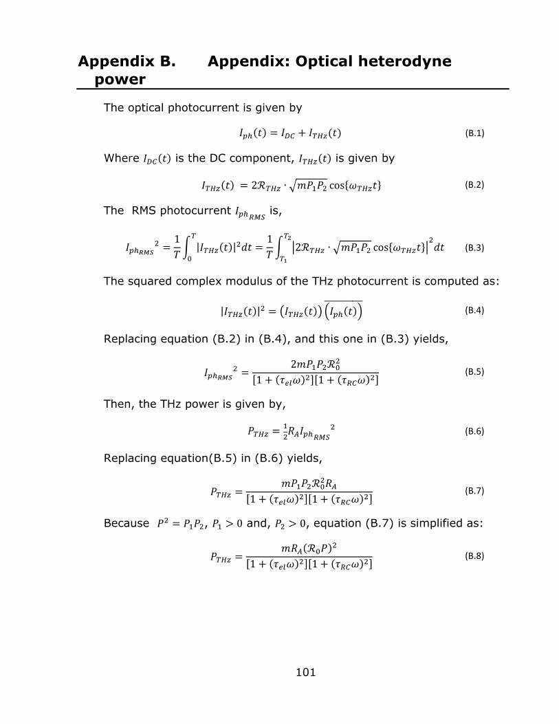
101
Appendix B. Appendix: Optical heterodyne
power
The optical photocurrent is given by
𝐼𝑝ℎ(𝑡) = 𝐼𝐷𝐶 + 𝐼𝑇𝐻𝑧(𝑡) (B.1)
Where 𝐼𝐷𝐶(𝑡) is the DC component, 𝐼𝑇𝐻𝑧(𝑡) is given by
𝐼𝑇𝐻𝑧(𝑡) = 2ℛ𝑇𝐻𝑧 ∙ √𝑚𝑃1𝑃2 cos𝜔𝑇𝐻𝑧𝑡 (B.2)
The RMS photocurrent 𝐼𝑝ℎ𝑅𝑀𝑆 is,
𝐼𝑝ℎ𝑅𝑀𝑆
2 =1
𝑇∫ |𝐼𝑇𝐻𝑧(𝑡)|
2𝑑𝑡𝑇
0
=1
𝑇∫ |2ℛ𝑇𝐻𝑧 ∙ √𝑚𝑃1𝑃2 cos𝜔𝑇𝐻𝑧𝑡|
2𝑑𝑡
𝑇2
𝑇1
(B.3)
The squared complex modulus of the THz photocurrent is computed as:
|𝐼𝑇𝐻𝑧(𝑡)|2 = (𝐼𝑇𝐻𝑧(𝑡)) (𝐼𝑝ℎ(𝑡))
(B.4)
Replacing equation (B.2) in (B.4), and this one in (B.3) yields,
𝐼𝑝ℎ𝑅𝑀𝑆
2 =2𝑚𝑃1𝑃2ℛ0
2
[1 + (𝜏𝑒𝑙𝜔)2][1 + (𝜏𝑅𝐶𝜔)2] (B.5)
Then, the THz power is given by,
𝑃𝑇𝐻𝑧 =1
2𝑅𝐴𝐼𝑝ℎ𝑅𝑀𝑆
2 (B.6)
Replacing equation(B.5) in (B.6) yields,
𝑃𝑇𝐻𝑧 =𝑚𝑃1𝑃2ℛ0
2𝑅𝐴
[1 + (𝜏𝑒𝑙𝜔)2][1 + (𝜏𝑅𝐶𝜔)2] (B.7)
Because 𝑃2 = 𝑃1𝑃2, 𝑃1 > 0 and, 𝑃2 > 0, equation (B.7) is simplified as:
𝑃𝑇𝐻𝑧 =𝑚𝑅𝐴(ℛ0𝑃)2
[1 + (𝜏𝑒𝑙𝜔)2][1 + (𝜏𝑅𝐶𝜔)2] (B.8)

102
Appendix C. Relevant Scattering lengths
The electron-phonon scattering length is calculated as [99]:
𝐿𝑒−𝑝ℎ = √𝐷𝑒𝜏𝑒−𝑝ℎ (C.1)
where 𝐷𝑒 is the coefficient diffusion for electrons, 𝜏𝑒−𝑝ℎ is the electron-phonon
scattering time which is calculated as [100]:
1
𝜏𝑒−𝑝ℎ=
𝑛𝑒𝜖12𝜔
𝜌𝑉2𝑘𝐵𝑇√
𝜋𝑚∗𝑉2
2𝑘𝐵𝑇exp(−
𝑚∗𝑉2
2𝑘𝐵𝑇) (C.2)
where 𝑛𝑒 is the concentration of conduction electrons, 𝜖1 is the deformation
potential, 𝜌 is the mass density, 𝑚∗ is the effective mass, 𝑉 is the phonon
group velocity, 𝜔 is the phonon frequency, 𝑘𝐵 is the Boltzmann equation, 𝑇 is
the temperature. The electron conductions for InP was assumed to be equal
to InGaAs Absorption layer because it is assumed that there is not electron-
phonon pairs and it is calculated by the mass action law (𝑛0 ≅ 𝑛𝑖2 𝑁𝐴⁄ , were 𝑛0
is the minority carriers concentration, 𝑛𝑖 the intrinsic carrier concentration and,
𝑁𝐴 the concentration of aceptor atoms) [101, pp. 90–95].
Table Appendix C.1. Value parameters and results used in equation (C.1)
and (C.2).
units In1-xGaxAs InP 𝑛𝑖 cm-3 6.3 × 10¹¹ 1.3 × 10⁷
𝑛𝑒 cm-3 4.0 × 10⁹ 4.0 × 10⁹
𝜖1 eV 7 7
𝜌 g/cm3 5.5 4.81
𝑚∗ Kg 3.7 × 10⁻³² 7.28 × 10⁻³²
𝑉 cm/s 3.7 × 10⁻³² 3.7 × 10⁻³²
𝑇 K 300 300
𝜔 Hz 7.2 × 10¹² 9.95 × 10¹²
𝐷𝑒 cm2/s 300 130 𝜏𝑒−𝑝ℎ s 8.1 × 10⁻¹⁵ 3.9 × 10⁻¹⁵
𝐿𝑒−𝑝ℎ m 1.6 × 10⁻⁸ 7.1 × 10⁻⁹
The data were obtained from reference [102].
The electron-electron scattering length is calculated as [103]:

103
𝐿𝑒−𝑒 = 𝑣𝐹𝜏𝑒−𝑒 (C.3)
where 𝑣𝐹 is the Fermi velocity, 𝜏𝑒−𝑒 is the electron-electron scattering time and
it is calculated as [103]:
1
𝜏𝑒−𝑒=
𝐸𝐹
ℎ(𝑘𝐵𝑇
𝐸𝐹)
2
[ln (𝐸𝐹
𝑘𝐵𝑇) + ln (
2𝑞
𝑘𝐹) + 1] (C.4)
Here 𝑞 is the 2D Thomas-Fermi screening wave vector (𝑞 =
𝑚∗𝑒2 2𝜋휀𝑟휀0ℏ2⁄ ), 𝐸𝐹 is the Fermi-level energy, 𝑘𝐹 is the Fermi wave vector (𝑘𝐹 =
(9𝜋 4⁄ )1 3⁄ 𝑟𝑠⁄ , with 𝑟𝑠 = (3 4𝜋𝑛⁄ )1 3⁄ and, 𝑛 the number of conduction electrons per
cubic centimeter[104]). The Fermi velocity is calculated as 𝑣𝐹 = ℏ𝑘𝐹 𝑚∗⁄ [105,
p. 333] [106, p. 13]. The Fermi energy value used here was the intrinsic value
because it was impossible to get real Fermi values for doped-semiconductors
in literature. The Fermi level was calculated as:
𝐸𝐹 =𝐸𝑔
2+
𝑘𝐵𝑇
2ln (
𝑁𝑉
𝑁𝐶) (C.5)
where 𝐸𝑔 is the energy bandgap, 𝑁𝑉 and 𝑁𝐶 are the effective density of states
for the valence and conduction bands.
Table Appendix C.2. Value parameters and results used in equation (C.3)
and (C.4).
units In0.53Ga0.47As InP 𝑁 cm-3 1 × 10¹⁸ 1 × 10¹⁶
𝑛 cm-3 1 × 10¹⁸ 1 × 10¹⁶
𝑁𝐶 cm-3 2.1 × 10¹⁷ 5.7 × 10¹⁷ 𝑁𝑉 cm-3 7.7 × 10¹⁸ 1.1 × 10¹⁹
𝑛𝑖 cm-3 6.3 × 10¹¹ 8.6 × 10⁷
𝑇 K 300 300
𝜏𝑒−𝑒 s 2.0 × 10⁻¹³ 3.1 × 10⁻¹³ 𝐿𝑒−𝑒 m 1.3 × 10⁻⁹ 1.0 × 10⁻⁹

104
Appendix D. Analytical model
Figure Appendix D-1a shows the transversal section of a Coplanar Waveguide
where inside this is represented the conductance and the capacitance. The piece of
waveguide of infinitesimal length Δ𝑧 of Figure Appendix D-1a can be modeled as a
lumped-element circuit, as shown in Figure Appendix D-1b, where R, L, G, C per unit
length quantities defined as follows:
𝑅1 and 𝑅2 = series resistances per unit length, for both conductors, in Ω/𝑚.
𝐿1 and 𝐿2 = series inductances per unit length, for both striplines conductors, in
𝐻/𝑚.
𝐺1 and 𝐺2 = shunt conductances per unit length, in 𝑆/𝑚.
𝐶1 and 𝐶2 = shunt capacitances per unit length, in 𝐹/𝑚.
The series inductance 𝐿1 and 𝐿2 represent the total self-inductance of the two
stripline conductors, and the shunt capacitance 𝐶1 and 𝐶2 is due to the close proximity
of the stripline conductors. The series resistances 𝑅1 and 𝑅2 represents the resitance
due to the finite conductivity of the conductors, and the shunt conductances 𝐺1 and
𝐺2 is due to dielectric loss in the material between the conductors. A finite length of
waveguide can be viewed as a cascade of sections of the form shown in Figure
Appendix D-1b.

105
a)
b)
Figure Appendix D-1. a) Conductance and capacitance represented
on the waveguide. b) Voltage and current definitions and equivalent circuit for an incremental length of transmission line.
Taking as a reference the Figure Appendix D-2, applying the Kirchhoff’s voltage
law to the mesh for the current 𝑖𝑎, the following equations:
1 1 1 1 2 2, , 0a ba
a a b
i iiv z t L z R Zi v z z t R z i i L z
t t
(1.1)
1 ai i (1.2)
2a bi i i (1.3)
Equation (1.2) is replaced in (1.3) and this result together equation (1.2)
is replaced in equation (1.1) to get:

106
Figure Appendix D-2. Kirchhoff’s voltage law circuit.
1 1 21
1 1 1 1 1 2 1 1 2 2, , 0i i ii
v z t L z R Zi v z z t R z i i i L zt t
(1.4)
Therefore, after symplifying equation (1.4) the next equation follows:
1 21 1 1 1 1 2 2 2, , 0
i iv z t L z R Zi v z z t R zi L z
t t
(1.5)
Equation (1.5) is rewritten as follow:
1 21 1 1 1 1 2 2 2, ,
i iv z z t v z t L z R Zi R zi L z
t t
(1.6)
Equation (1.6) is divided by Δ𝑧:
1 2
1 1 1 2 2 21 1, ,
i iL z R Zi R zi L zv z z t v z t t t
z z
(1.7)
Equation (1.7) is simplified:
1 1 1 21 1 1 2 2 2
, ,v z z t v z t i iL R i R i L
z t t
(1.8)
The limit when Δ𝑧 tends to 0 is applied to equation (1.8):

107
1 1 1 21 1 1 2 2 2
0 0
, ,lim limz z
v z z t v z t i iL R i R i L
z t t
(1.9)
The first differential equation as a part of a set of differential equations is defined
from equation (1.9):
1 1 21 1 1 2 2 2
v i iL R i R i L
z t t
(1.10)
A similar procedure is applied for the mesh of the current 𝑖𝑏. Therefore, after
applying the Kirchhoff’s voltage law, the following equation is obtained:
2 2 2 2, , 0b a
b a
i iv z t L z R Z i i v z z t
t
(1.11)
1 ai i (1.12)
2a bi i i (1.13)
Therefore,
(1.14)
Replacing equations (1.12) and (1.14) in equation (1.11) to get:
2
2 2 2 2 2, , 0i
v z t L z R z i v z z tt
(1.15)
Simplifying and rewriting:
2
2 2 2 2 2, , 0i
v z t L z R z i v z z tt
2
2 2 2 2 2, ,i
v z z t v z t L z R z it
(1.16)
Equation (1.16) is divided by Δ𝑧:
2
2 2 22 2, ,
iL z R z iv z z t v z t t
z z
(1.17)
Equation (1.17) is simplified:

108
2 2 22 2 2
, ,v z z t v z t iL R i
z t
(1.18)
The limit when Δ𝑧 tends to 0 is applied to equation (1.18):
2 2 22 2 2
0 0
, ,lim limz z
v z z t v z t iL R i
z t
(1.19)
Finally the last equation is:
2 22 2 2
v iL R i
z t
(1.20)
Taking Figure Appendix D-3 as a reference and seeing that this is a modified plot
of Figure Appendix D-3 and applying Kirchhoff’s current law circuit to the node (1)
the following equation is obtained:
1 1 ,ai i i z z t (1.21)
Applying Kirchhoff’s current law to the node (2):
1
1 1 1
,,a b c
v z z ti i i v z z t G z C z
t
(1.22)
Figure Appendix D-3. Kirchhoff’s current law circuit.

109
Equation (1.22) is replaced in equation (1.21):
1
1 1 1 1 1
,, ,
v z z ti v z z t G z C z i z z t
t
(1.23)
Equation (1.23) is simplified as follow:
1
1 1 1 1 1
,, ,
v z z ti z z t i v z z t G z C z
t
(1.24)
Equation (1.24) is divided by Δ𝑧 and later it is applied a limit when Δ𝑧 tends to 0:
1 1 1
1 1 10 0
, ,lim lim ,z z
i z z t i v z z tv z z t G C
z t
(1.25)
The third equation is established:
11
1 1 1
,,
v z tiG v z t C
z t
(1.26)
The last equation is obtained using Kirchhoff’s current law to the node
(3):
2 2 ,a di i i i z z t (1.27)
The equation for the node (4) is:
2
2 2 2
,,d e f
v z z ti i i v z z t G z C z
t
(1.28)
The equations (1.22) and (1.28) is replaced in (1.27)
1 2
2 1 1 1 2 2 2 2
, ,, , ,
v z z t v z z ti v z z t G z C z v z z t G z C z i z z t
t t
(1.29)
The equation (1.29) is rewritten as:
1 2
2 2 1 1 1 2 2 2
, ,, , ,
v z z t v z z ti z z t i v z z t G z C z v z z t G z C z
t t
(1.30)
The equation (1.30) is divided by Δ𝑧 and a limit when Δ𝑧 tends to zero:

110
2 2 1 2
1 1 1 2 2 20 0
, , ,lim lim , ,z z
i z z t i v z z t v z z tG v z z t C G v z z t C
z t t
(1.31)
Evaluating the limit finally is the last equation:
1 22
1 1 1 2 2 2
, ,, ,
v z t v z tiG v z t C G v z t C
z t t
(1.32)
Therefore, the following equation set is established:
1 1 21 1 1 2 2 2
( , ) ( , ) ( , )( , ) ( , )
v z t i z t i z tL R i z t R i z t L
z t t
(1.33)
2 22 2 2
( , ) ( , )( , )
v z t i z tL R i z t
z t
(1.34)
11
1 1 1
,( , ),
v z ti z tG v z t C
z t
(1.35)
1 22
1 1 1 2 2 2
, ,( , ), ,
v z t v z ti z tG v z t C G v z t C
z t t
(1.36)
These equations are the time domain form of the transmission line, or telegrapher,
equations. For the sinusoidal steady-state condition, with cosine-based phasors,
equations (1.33) to (1.36) simplify to:
11 1 1 2 2 2
( )dV zj L R I z j L R I z
dz (1.37)
2
2 2 2
dV zj L R I z
dz (1.38)
1
1 1 1
dI zG j C V z
dz (1.39)
2
1 1 1 2 2 2
dI zG j C V z G j C V z
dz (1.40)
The partial differential equations system (1.37) - (1.40) can be written in vectorial
notation as follows. A matrix 𝐴(𝑧):

111
1 1 2 2
2 2
1 1
1 1 2 2
0 0
0 0 0
0 0 0
0 0
j L R j L R
j L RA z
G j C
G j C G j C
(1.41)
The vector X and its derivative X’ is written as:
1
2
1
2
V z
V z
I z
I z
x (1.42)
1
2
1
2
'
dV z
dz
dV z
dz
dI z
dz
dI z
dz
x (1.43)
Therefore, the partial differential equations system (1.37) - (1.40):
' z z zx A x (1.44)
The MuPAD solver was used:
The partial differential equations system (1.37) - (1.40) can be written in vectorial
notation as follows. A matrix 𝐴(𝑧):
1 1 2 2
2 2
1 1
1 1 2 2
0 0
0 0 0
0 0 0
0 0
j L R j L R
j L RA z
G j C
G j C G j C
(1.45)
By setting the following equivalences:
1 1
2 2
1 1
2 2
A j L R
B j L R
C G j C
D G j C
(1.46)

112
Equation is re-written as:
0 0
0 0 0
0 0 0
0 0
A B
BA z
C
C D
(1.47)
The vector X and its derivative X’ is written as:
1
2
1
2
V z
V z
I z
I z
x (1.48)
1
2
1
2
'
dV z
dz
dV z
dz
dI z
dz
dI z
dz
x (1.49)
Therefore, the partial differential equations system (1.37) - (1.40):
' z z zx A x (1.50)
In order to solve equation (1.44), the characteristic polynomial:
det I A (1.51)
Which solved is given by:
4 2BC AC BD ABCD (1.52)
Whose roots are:

113
2 2 2 2 2 2 2 2
1
2 2 2 2 2 2 2 2
2
2 2 2 2 2 2 2 2
3
2 2 2 2 2 2 2 2
4
2 2 2
2 2 2 2
2 2 2
2 2 2 2
2 2 2
2 2 2 2
2 2 2
2 2 2 2
AC A C ABC ABCD B C B CD B D BC BD
A C ABC ABCD B C B CD B D AC BC BD
AC A C ABC ABCD B C B CD B D BC BD
A C ABC ABCD B C B CD B D AC BC BD
(1.53)
The roots (1.53) are the eigenvalues of the matrix (1.45).
The eigenvectors for 𝜆1, 𝜆2, 𝜆3 and 𝜆4 are calculated according to:
1 4 I A v 0 (1.54)
For the eigenvalue 𝜆1, the eigenvector is given by:
4 3
5 1
1
2
1
v (1.55)
With multiplicity 1.
The solution 𝑿1 using the eigenvector 𝑽1 is calculated as:
1
1 1
zz e
x v (1.56)
For the eigenvalue 𝜆2, the eigenvector is given by:
10 9
11 6
2
8
1
v (1.57)
With multiplicity 1.
The solution 𝑿2 using the eigenvector 𝑽2 is calculated as:
2
2 2
zz e
x v (1.58)
For the eigenvalue 𝜆3, the eigenvector is given by:

114
4 3
5 1
3
2
1
v (1.59)
With multiplicity 1.
The solution 𝑿3 using the eigenvector 𝑽3 is calculated as:
3
3 3
zz e
x v (1.60)
For the eigenvalue 𝜆4, the eigenvector is given by:
10 9
11 6
4
8
1
v (1.61)
With multiplicity 1.
The solution 𝑿4 using the eigenvector 𝑽4 is calculated as:
4
4 4
zz e
x v (1.62)
The general solution is given by:
1 1 2 2 3 3 4 4z c z c z c z c z x x x x x (1.63)
31 2 4
1
2
1 1 2 2 3 3 4 4
1
2
zz z z
V z
V zc e c e c e c e
I z
I z
v v v v (1.64)
31 2 4
1 4 3 10 9 4 3 10 9
2 5 1 11 6 5 1 11 6
1 2 3 4
1 2 8 2 8
2 1 1 1 1
zz z z
V z
V zc e c e c e c e
I z
I z
(1.65)
31 2 4
31 2 4
31 2 4
31 2 4
1 1 4 3 2 10 9 3 4 3 4 10 9
2 1 5 1 2 11 6 3 5 1 4 11 6
1 1 2 2 8 3 2 4 8
2 1 2 3 4
zz z z
zz z z
zz z z
zz z z
V z c e c e c e c e
V z c e c e c e c e
I z c e c e c e c e
I z c e c e c e c e
(1.66)

115
Where the constants 𝜎1 to 𝜎16 are defined as follow:
13 12
1
1614
2
14 12
3 2
3/2
12
4 2
3/2
12
5
13 15
6
15 14
8
14 15
9 2
3/2
15
10 2
3/2
15
11
12 16
13
14
15 16
2 2 2
2 2 2
2 2 2
ACD
AC BC BD
AC AC
AC
AC
ACD
ACD
AC AC
AC
AC
ACD
AC BC BD
BC AC BD
BC BD
AC BC BD
2 2 2 2 2 2 2 2
16
2 2 2
2
A C ABC ABCD B C B CD B D
(1.67)
The MuPAD solver was used:
The partial differential equations system (1.37) - (1.40) can be written in vectorial
notation as follows. A matrix 𝐴(𝑧):
1 1 2 2
2 2
1 1
1 1 2 2
0 0
0 0 0
0 0 0
0 0
j L R j L R
j L RA z
G j C
G j C G j C
(1.68)
By setting the following equivalences:

116
1 1
2 2
1 1
2 2
A j L R
B j L R
C G j C
D G j C
(1.69)
Equation is re-written as:
0 0
0 0 0
0 0 0
0 0
A B
BA z
C
C D
(1.70)
The vector X and its derivative X’ is written as:
1
2
1
2
V z
V z
I z
I z
x (1.71)
1
2
1
2
'
dV z
dz
dV z
dz
dI z
dz
dI z
dz
x (1.72)
Therefore, the partial differential equations system (1.37) - (1.40):
' z z zx A x (1.73)
In order to solve equation (1.44), the characteristic polynomial:
det I A (1.74)
Which solved is given by:
4 2BC AC BD ABCD (1.75)
Whose roots are:

117
2 2 2 2 2 2 2 2
1
2 2 2 2 2 2 2 2
2
2 2 2 2 2 2 2 2
3
2 2 2 2 2 2 2 2
4
2 2 2
2 2 2 2
2 2 2
2 2 2 2
2 2 2
2 2 2 2
2 2 2
2 2 2 2
AC A C ABC ABCD B C B CD B D BC BD
A C ABC ABCD B C B CD B D AC BC BD
AC A C ABC ABCD B C B CD B D BC BD
A C ABC ABCD B C B CD B D AC BC BD
(1.76)
The roots (1.53) are the eigenvalues of the matrix (1.45).
The eigenvectors for 𝜆1, 𝜆2, 𝜆3 and 𝜆4 are calculated according to:
1 4 I A v 0 (1.77)
For the eigenvalue 𝜆1, the eigenvector is given by:
4 3
5 1
1
2
1
v (1.78)
With multiplicity 1.
The solution 𝑿1 using the eigenvector 𝑽1 is calculated as:
1
1 1
zz e
x v (1.79)
For the eigenvalue 𝜆2, the eigenvector is given by:
10 9
11 6
2
8
1
v (1.80)
With multiplicity 1.
The solution 𝑿2 using the eigenvector 𝑽2 is calculated as:
2
2 2
zz e
x v (1.81)
For the eigenvalue 𝜆3, the eigenvector is given by:

118
4 3
5 1
3
2
1
v (1.82)
With multiplicity 1.
The solution 𝑿3 using the eigenvector 𝑽3 is calculated as:
3
3 3
zz e
x v (1.83)
For the eigenvalue 𝜆4, the eigenvector is given by:
10 9
11 6
4
8
1
v (1.84)
With multiplicity 1.
The solution 𝑿4 using the eigenvector 𝑽4 is calculated as:
4
4 4
zz e
x v (1.85)
The general solution is given by:
1 1 2 2 3 3 4 4z c z c z c z c z x x x x x (1.86)
31 2 4
1
2
1 1 2 2 3 3 4 4
1
2
zz z z
V z
V zc e c e c e c e
I z
I z
v v v v (1.87)
31 2 4
1 4 3 10 9 4 3 10 9
2 5 1 11 6 5 1 11 6
1 2 3 4
1 2 8 2 8
2 1 1 1 1
zz z z
V z
V zc e c e c e c e
I z
I z
(1.88)
31 2 4
31 2 4
31 2 4
31 2 4
1 1 4 3 2 10 9 3 4 3 4 10 9
2 1 5 1 2 11 6 3 5 1 4 11 6
1 1 2 2 8 3 2 4 8
2 1 2 3 4
zz z z
zz z z
zz z z
zz z z
V z c e c e c e c e
V z c e c e c e c e
I z c e c e c e c e
I z c e c e c e c e
(1.89)

119
Where the constants 𝜎1 to 𝜎16 are defined as follow:
13 12
1
1614
2
14 12
3 2
3/2
12
4 2
3/2
12
5
13 15
6
15 14
8
14 15
9 2
3/2
15
10 2
3/2
15
11
12 16
13
14
15 16
2 2 2
2 2 2
2 2 2
ACD
AC BC BD
AC AC
AC
AC
ACD
ACD
AC AC
AC
AC
ACD
AC BC BD
BC AC BD
BC BD
AC BC BD
2 2 2 2 2 2 2 2
16
2 2 2
2
A C ABC ABCD B C B CD B D
(1.90)

120
Appendix E. Supplemental Material
Figure Appendix E-1. Cross sectional representation of the electric field at
the center of the transmission line, which have a n-layer doping of 50000 S/m, at a frequency of 500 GHz. The arrows flows symmetrical from the
center stripline to the lateral striplines.
Figure Appendix E-2. Cross sectional representation of the electric field at the center of the transmission line, which have a n-layer doping of 50000
S/m, at a frequency of 1000 GHz. The arrows flows symmetrical from the center stripline to the lateral striplines.

121
Figure Appendix E-3. Cross sectional representation of the electric field at
the center of the transmission line, which have a n-layer doping of 50000 S/m, at a frequency of 2000 GHz. The arrows flows symmetrical from the
center stripline to the lateral striplines.

122
a)
b)
Figure Appendix E-4. Color plot of a cross-section of a UTC-PD device. The image shows an enlarged section of the device where the zoom is applied on
the central stripline, lateral striplines, and the n-doped layer. This layer has a conductivity of 1.0 × 10⁻¹ S/m and at a frequency of 100 GHz. a) Electric
Field. b) Magnetic Field.

123
a)
b)
Figure Appendix E-5. Color plot of a cross-section of a UTC-PD device. The
image shows an enlarged section of the device where the zoom is applied on the central stripline, lateral striplines, and the n-doped layer. This layer has
a conductivity of 2.1 × 10³ S/m and at a frequency of 100 GHz. a) Electric
Field. b) Magnetic Field.

124
a)
b)
Figure Appendix E-6. Color plot of a cross-section of a UTC-PD device. The image shows an enlarged section of the device where the zoom is applied on
the central stripline, lateral striplines, and the n-doped layer. This layer has a conductivity of 5 × 10⁴ S/m and at a frequency of 100 GHz. a) Electric Field.
b) Magnetic Field.

125
a)
b)
Figure Appendix E-7. Color plot of a cross-section of a UTC-PD device. The image shows an enlarged section of the device where the zoom is applied on
the central stripline, lateral striplines, and the n-doped layer. This layer has a conductivity of 1.7 × 10⁵ S/m and at a frequency of 100 GHz. a) Electric
Field. b) Magnetic Field.

126
a)
b)
Figure Appendix E-8. Color plot of a cross-section of a UTC-PD device. The image shows an enlarged section of the device where the zoom is applied on
the central stripline, lateral striplines, and the n-doped layer. This layer has a conductivity of 4.5 × 10⁷ S/m and at a frequency of 100 GHz. a) Electric
Field. b) Magnetic Field.

127
a)
b)
Figure Appendix E-9. Color plot of a cross-section of a UTC-PD device. The image shows an enlarged section of the device where the zoom is applied on
the central stripline, lateral striplines, and the n-doped layer. This layer has a conductivity of 1.0 × 10⁻¹ S/m and at a frequency of 1000 GHz. a) Electric
Field. b) Magnetic Field.

128
a)
b)
Figure Appendix E-10. Color plot of a cross-section of a UTC-PD device. The image shows an enlarged section of the device where the zoom is applied
on the central stripline, lateral striplines, and the n-doped layer. This layer has a conductivity of 2.1 × 10³ S/m and at a frequency of 1000 GHz. a) Electric
Field. b) Magnetic Field.

129
a)
b)
Figure Appendix E-11. Color plot of a cross-section of a UTC-PD device. The image shows an enlarged section of the device where the zoom is applied
on the central stripline, lateral striplines, and the n-doped layer. This layer has a conductivity of 5 × 10⁴ S/m and at a frequency of 1000 GHz. a) Electric
Field. b) Magnetic Field.

130
a)
b)
Figure Appendix E-12. Color plot of a cross-section of a UTC-PD device. The image shows an enlarged section of the device where the zoom is applied
on the central stripline, lateral striplines, and the n-doped layer. This layer has a conductivity of 1.7 × 10⁵ S/m and at a frequency of 1000 GHz. a) Electric
Field. b) Magnetic Field.

131
a)
b)
Figure Appendix E-13. Color plot of a cross-section of a UTC-PD device. The image shows an enlarged section of the device where the zoom is applied
on the central stripline, lateral striplines, and the n-doped layer. This layer has a conductivity of 4.5 × 10⁷ S/m and at a frequency of 1000 GHz. a) Electric
Field. b) Magnetic Field.

132
a)
b)
Figure Appendix E-14. Color plot of a cross-section of a UTC-PD device. The image shows an enlarged section of the device where the zoom is applied
on the central stripline, lateral striplines, and the n-doped layer. This layer has a conductivity of 1.0 × 10⁻¹ S/m and at a frequency of 2000 GHz. a)
Electric Field. b) Magnetic Field.

133
a)
b)
Figure Appendix E-15. Color plot of a cross-section of a UTC-PD device. The image shows an enlarged section of the device where the zoom is applied
on the central stripline, lateral striplines, and the n-doped layer. This layer has a conductivity of 2.1 × 10³ S/m and at a frequency of 2000 GHz. a) Electric
Field. b) Magnetic Field.

134
a)
b)
Figure Appendix E-16. Color plot of a cross-section of a UTC-PD device. The image shows an enlarged section of the device where the zoom is applied
on the central stripline, lateral striplines, and the n-doped layer. This layer has a conductivity of 5 × 10⁴ S/m and at a frequency of 2000 GHz. a) Electric
Field. b) Magnetic Field.

135
a)
b)
Figure Appendix E-17. Color plot of a cross-section of a UTC-PD device. The image shows an enlarged section of the device where the zoom is applied
on the central stripline, lateral striplines, and the n-doped layer. This layer has a conductivity of 1.7 × 10⁵ S/m and at a frequency of 2000 GHz. a) Electric
Field. b) Magnetic Field.

136
a)
b)
Figure Appendix E-18. Color plot of a cross-section of a UTC-PD device. The image shows an enlarged section of the device where the zoom is applied
on the central stripline, lateral striplines, and the n-doped layer. This layer has a conductivity of 4.5 × 10⁷ S/m and at a frequency of 2000 GHz. a) Electric
Field. b) Magnetic Field.