Embed Size (px)
Citation preview
r AD-A115 069 ELECTRO MNETIC APPLICATIONS INC GOLDE N CO F/4 1/3COUPLING OF LIGHTNING STROKE CURRENT TO AIRCRAFT BALANCED TVIST--ETC (U)
06 MAR 79 ft B COOK, R A PERALA NOO019-79-4-0584
UNCLASSIFIED NL
IllluuuuuuuuumEllEEEEilEEEEEE*uuuuuuuuumI

1.11112.
H ,L1_.25 _____ 12

QAIR-518:5
COUPLING OF LIGHTNING STROKECURRENT TO AIRCRAFT BALANCEDTWISTED SHIELDED PAIR CABLES
iss
7-Y- 4?- 3
CD NAVAL AIR SYSTEM COMMAND
U.S. DEPARTMENT OF THE NAVY
APPROVED FOR PUBLIC REL.E:
DISTRIBUTION UNUMITE
82 06 01 029

ELECTRO MAGNGT!C
P -.. ox.
-Golden, Colorado 80401 - A
.74 COUPLING~ UF.U-IHTNING STROKE CUR:NTS70-F-18 *
BAL.ANrED TWISTED SHIELDED'PAIR CABLE-. ~ ,*
- 3. -
'Poraa i. ,.j~,-~- oi.
Wahigtn D.. C., 2036
111 -* -# d
* JAA * - .~ *bA .
- - .. ~*~.AAA~A,~Dl. a* B U fAA

TABLE OF CONTENTS
Page
CHAPTER 1 - Introduction- -------------- 1
CHAPTER 2 - F-18 Lightning Coupling Paths Through
the Avionics Bay Access Doors----- 4
CHAPTER 3 - F-18 Shielding and Cabling Practices - - 9
CHAPTER 4 - The Overall Coupling Model and NumericalResults ------ ------ ---- 17
CHAPTER 5 - Summary and Conclusions-------- -- 25
REFERENCES ------- ------ ------ -- 27
APPENDIX A - The Formulation of the-BTSP ComputerProgram ------ ------ ---- 28
A0@SSsion ForDTIC TAS 0
|ul3n@uncejustbLyiatIOn--
Distribution/OAVaU biy Codes
..... anadfor
Ditt Special
LIST OF ILLUSTRATIONS
Page
Figure 1 F-18 Materials Distribution ---- -- ------ ---- 2
Figure 2 Lightning Return Stroke Current Used in the DirectStroke Analysis -- -- ---------------- 4
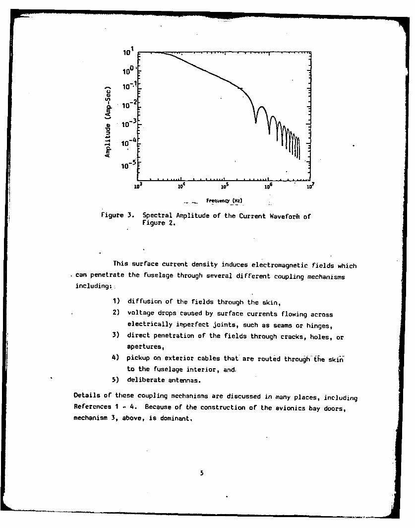
Figure 3 Spectral Amplitude of the Current Waveform offigure 2- --- ------------ ------- 5
Figure 4 Illustration of Avionics Bay Doors Construction -- 6
Figure 5 Inner Conductor Equivalent Circuit when Both theTransfer Impedance and the Transfer Admittanceare Included -- ------- ------------ 10
Figure 6 Transfer Impedance of Braided and Solid OuterConductor Coaxial Cable- -- ---------- --- 11
Figure 7 Braided Pattern Developed on a Plane -- -------- 12
Figure 8 Braid Angle [2]- -- ------- ----------- 14
Figure 9 S.E. Change with Percent Optical Coverage (2] - - 14
Figure 10 Two BTSP Cables- -- ------- ----------- 15
Figure 11 Pictorial Representation of Overall Coupling
Problem- -- ------ --------------- 17
Figure 12 A Slot Antenna and Its Complementary Strip Dipole - 18
Figure 13 Equivalent Circuit of the Avdonics Bay Coupling.Mechanism- -- ------ -------------- 20
Figure 14 Wire Configuration for Worst Case CurrentDivision- --- ----------- ------- 21
Figure 15 Induced BTSP Common Mode Voltages for Worst CaseDivision- --- -------- -- ---------- 24
Figure 16 Lightning Stroke Current Probability Curve - - - - 25

LIST OF TABLES
Page
TABLE I F-18 Avionics* Bay Access Doors -- -- ------------ 7
TABLE 2 Parameters of the Two BISP Cables- -- ---------- 16
TABLE 3 Summary of Values for Current Division -- -- ------- 22
TABLE 4 Summary of Coupling Results (Volts)- -- --------- 23
TABLE 5 Summary of Coupling Results for 200 KA LightningStrike- -- ------ ----- -- ------------
Wi
COUPLING OF LIGHTNING STROKE CURRENTS TO F-18
BALANCED TWISTED SHIELDED PAIR CABLES
CHAPTER 1
INTRODUCTION
The F-8 is the first military aircraft which makes extensive
use of graphite epoxy composite materials. These materials are used on
the wings, tail, horizontal stabilizer, and on various access doors and
panels. Figure 1 illustrates the usage locations. The aircraft also
uses fly-by-wire technology in all axes, although it has mechanical back-
up in all axes except for yaw. The aircraft can land at an airfield on
these backups alone, however, aircraft carrier landings ma' be somewhat
more hazardous. In addition, the aircraft avionics make extensive use of
low-level integrated circuit technology, including the flight control
computer,. the AYK-14.
In view of these facts, electromagnetic hazards assume a more
important role in aircraft survivability, both to man-made and natural
threats. In particular, the use of graphite epoxy composites implies a
shielding effectiveness which is less than that obtained on metallic air-
craft, because of the composite's smaller (by a factor of - 101) electrical
conductivity and the problem associated with obtaining good electrical
joints ,(composite/composite as well as metal/composite).
The scope of this investigation is not to investigate the suscepti-
bility of the aircraft to all electromaonetic threats. -Instead, one of the
threats of greatest concern, an attached lightning stroke, is the subject
of the investigation In particular, the threat caused by a direct strike
to the nose/tail is examined for the cables which route across access doors
of composite/aluminum hoeycomb construction with special treatment of the
edges to avoid corrosion. '\There is concern that, because of the proximity
1I

%7
. . Perce nt of
. " - Sic, .Weight
A~~wm~nwt- .......48
steel ................ I .S
Titanium ............. 12.8r-77 Graphite/Epoxy ....... : 9.5,
Oihe ................ I1.4. 100.0
.a. Upper Fuselage.
--' ' . A',-
AA mmum.
lu .. ..... .
St eel ............." ;. Titanim um ..........
l Gaphot/pony .....otheui . ....
b. Lower Fuselage
Figure 1. F-18 Materials Distribution.
2
of these cables to these doors, lightning could induce spurious signals
in these cables large enough to either damage or upset the attached
electronics. These cables contain Balanced Twisted Shielded Pair (BTSP)
wiring. The objective of this study is to therefore determine the light-
ning induced voltages and currents on the BTSP inner wires.
The approach in this study is to first examine the lightning
threat and coupling paths to the F-18. Then the electromagnetic shielding
and pertinent wiring practices are described. An overall computerized
coupling model is then developed and implemented.
The analysis predicts that for a worst-case direct lightning
stroke, the voltages on the BTSP wiring will be within the range of' 16 to
175 volts. The differential mode is in the range of 0.5 to 5.3 volts.
3

CHAPTER 2
F-1O LIGHTNING COUPLING PATHS THROUGH THE
AVIONICS BAY ACCESS DOORS
This section describes how transients from a lightning stroke
attaching to the F-18 nose or tail can couple through the avionics bay
access doors to the BTSP cables routed nearby.
The lightning current used in this report is the worst-case
return stroke current of Figure 2, whose amplitude of 200,000 amperes
exceeds more than 99% of all lightning strokes. The average return stroke
current is on the order of 20,000 amperes. The spectral content in Fig-
ure 3 shows that lightning is mainly a low-frequency transient. The axial
current is assumed to distribute uniformly around the fuselage, and the
axial surface current density is therefore approximately
I 200 Ka 44 Ka/r,
s 2 2%xO.72m 0 K
where the O.72m radius of the fuselage at the avionics bay is used.
.5 I
200
I 100
psec 20 40 60 80 100 psec
Figure 2. Lightning Return Stroke Current Used inthe Direct Stroke Analysis.
4
101
100
10-1
, 10-
. 10-4
10o3 1 1o S1o 6 107
-- Frequency (Hz)
Figure 3. Spectral Amplitude of the Current Wavefor ofFigure 2.
This surface current density induces electromagnetic fields which
- can penetrate the fuselage through several different coupling mechanisms
including:..
1) diffusion of the fields through the skin,
2) voltage drops caused by surface currents flowing across
electrically imperfect joints, such as seams or hinges,
3) direct penetration of the fields through cracks, holes, or
apertures,
4) pickup on exterior cables that are routed through the skiito the fuselage interior, and.
5) deliberate antennas.
Details of these coupling mechanisms are discussed in many places, including
References I - 4. Because of the construction of the avionics bay doors,
mechanism 3, above, is dominant,
5
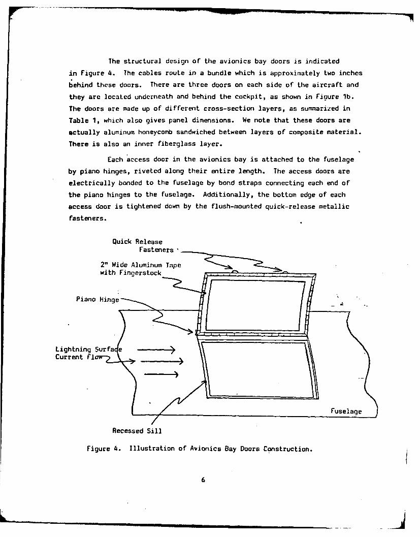
The structural design of the avionics bay doors is indicated
in Figure 4. The cables route in a bundle which is approximately two inches
behind these doors. There are three doors on each side of the aircraft and
they are located underneath and behind the cockpit, as shown in Figure lb.
The doors are made up of different cross-section layers, as summarized in
Table 1, which also gives panel dimensions. We note that these doors are
actually aluminum honeycomb sandwiched between layers of composite material.
There is also an inner fiberglass layer.
Each access door in the avionics bay is attached to the fuselage
by piano hinges, riveted along their entire length. The access doors are
electrically bonded to the fuselage by bond straps connecting each end of
the piano hinges to the fuselage. Additionally, the bottom edge of each
access door is tightened down by the flush-mounted quick-release metallic
fasteners.
Quick ReleaseFasteners.
2" Wide Aluminum Tapewith Fingerstock
Fuselage
Recessed Sill
Figure 4. Illustration of Avionics Bay Doors Construction.
6

TABLE 1.
F-18 AVIONICS BAY ACCESS DOORS
Panel Size
10 or 12 15" x 53"
13R or 13L 20" x 40"
14R or 14L 20" x 31"
Panel Cross-Section Construction
Outside Layer 5 ply Graphite Epoxy (5 mils/ply)
Middle Layer Aluminum Honeycomb, 150 mils thick
Inside Layer 5 ply Graphite Epoxy (5 mils/ply)
1 ply Fiberglass (5 mils/ply)
The layer of fiberglass is attached to the inside of the access
doors to reduce the corrosion problem which occurs when graphite epoxy
composites contact aluminum. A two-inch wide strip of aluminum tape with
EMI fingerstock is attached around the periphery of the fiberglass layer
to provide contact with the sill when the access doors are closed. However,
except at perhaps the piano hinge and the fasteners, the aluminum tape is
DC isolated (capacitively coupled) from the access door by the fiberglass
layer.
For a stroke to the nose or tail and exiting the tail or nose,
the surface current density in the vicinity of these doors is principally
axial and was previously calculated to be 44 Ka/m. If-the door did not- -
affect the surface current distribution, it would flow in a direction
parallel to the edges of the door which are DC connected, and normal to
the edges which are not DC connected. Thus the edges which are normal to
the flow are cracks which can be modelled as a capacitively loaded slot
antenna (Reference 1). The capacitance loading between the aluminum tape on
the access doors and the doorpanel on the fuselage, can be estimated by well-
known standard formulas for parallel plate capacitors, and one obtains
7

10.6 nt/n for a relative dielectric constant ot 3 tor the 5-mil layer ot
fiberglass. Corrosion and vibration at the access doors does not affect
this capacitance.
It is noted that these slots exist independently ot whether or
not the door edges parallel to the current flow are DC connected (which
they are). In addition, because there are three doors, there are six
slots.
For the purposes ot this investigation therefore, coupling of
the lightning current to the cables is limited to that caused by the afore-
mentioned slots which are normal to the axial lightning current flow. It
is noted that diffusion through the door is neglected. This is because the
aluminum honeycomb will tend to short out the electric field and reduce the
diffusion fields to a small value. The actual modelling of the slot coupling
is reserved for Chapter 4. Before this model is presented,~ the cabling and
shielding practices in the F-18 are discussed in Chapter 3, along with
features pertinent to the present analysis.
8
CHAPTER 3
F-l8 SHIELDING AND CABLING PRACTICES
The general design philosphy for EMI mitigation on internal
cables and boxes is to use filters or filter pin connectors at the box
inputs to reduce the high frequency signals, shielded cables to reduce
the middle frequencies, and balanced loads for the low frequencies.
Balanced Twisted Shielded Pair (BTSP) cables are frequently used to
implement this shielding philosophy, particularly for connections to the
flight control computer.
The physical layout of the cabling determines coupling to the
cables. The wires in the F-l8 are grouped together into wiring harnesses
(or bundles) about two inches in diameter and supported about two inches
away from the fuselage skin. A typical harness consists of many types of
cables, both shielded and unshielded, single and multiconductor. The ends
of the cable shields are brought out in pigtails four to eight inches
long and bonded to the electronic box shield (which is bonded to the air-
frame structure) via a connector pin. The connectors use plastic backshells,
which are lightweight but offer no shielding. Therefore, connector shielding
degradation caused by vibration and corrosion are not pertinent and thus not
considered here. Also, because lightning is of mainly low frequency content,
filter pin connectors offer little attenuation, and in fact can degrade dif-
ferential mode attenuation at the low frequencies.
Cable shielding will now be defined and discussed, first in
general terms, and then specifics relating to the BTSP will be given.
A shielded cable which routes over a structure or ground plane
allows spurious signals to appear on the inner conductors by two mechanisms:
the shield transfer impedance Z t Ma and the shield transfer admittance Y t M.
These are defined in terms of the shield current I (wM, shield -voltage with
respect to structure V S(w), the induced electric field E.(M, on the inside
of the shield, and the induced internal current sources per unit length
9
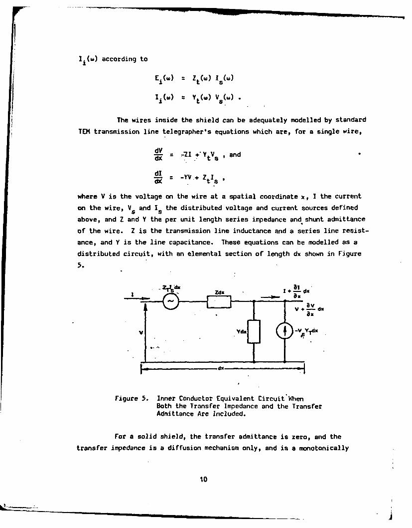
I(w) according to
El(W) =Zt(M I S(W)
Ii (W) Y ¥t(W) Vs6(W) •
The wires inside the shield can be adequately modelled by standard
TEN transmission line telegrapher's equations which are, for a single wire,
- = YtVs ,and
dl= -YV.+ Z I
where V is the voltage on the wire at a spatial coordinate x, I the current
on the wire, Vs and Is the distributed voltage and current sources defined
above, and Z and Y the per unit length series impedance and shunt admittance
of the wire. Z is the transmission line inductance and a series line resist-
ance, and Y is the line capacitance. These equations can be modelled as a
distributed circuit, with an elemental section of length dx shown in Figure
5.
V + V d,ax
V Ydm _vY-d
.- -
Figure 5. Inner Conductor Equivalent Circuit WhenBoth the Transfer Impedance and the TransferAdmittance Are Included.
For a solid shield, the transfer admittance is zero, and the
transfer impedance is a diffusion mechanism only, and is a monotonically
10
-j
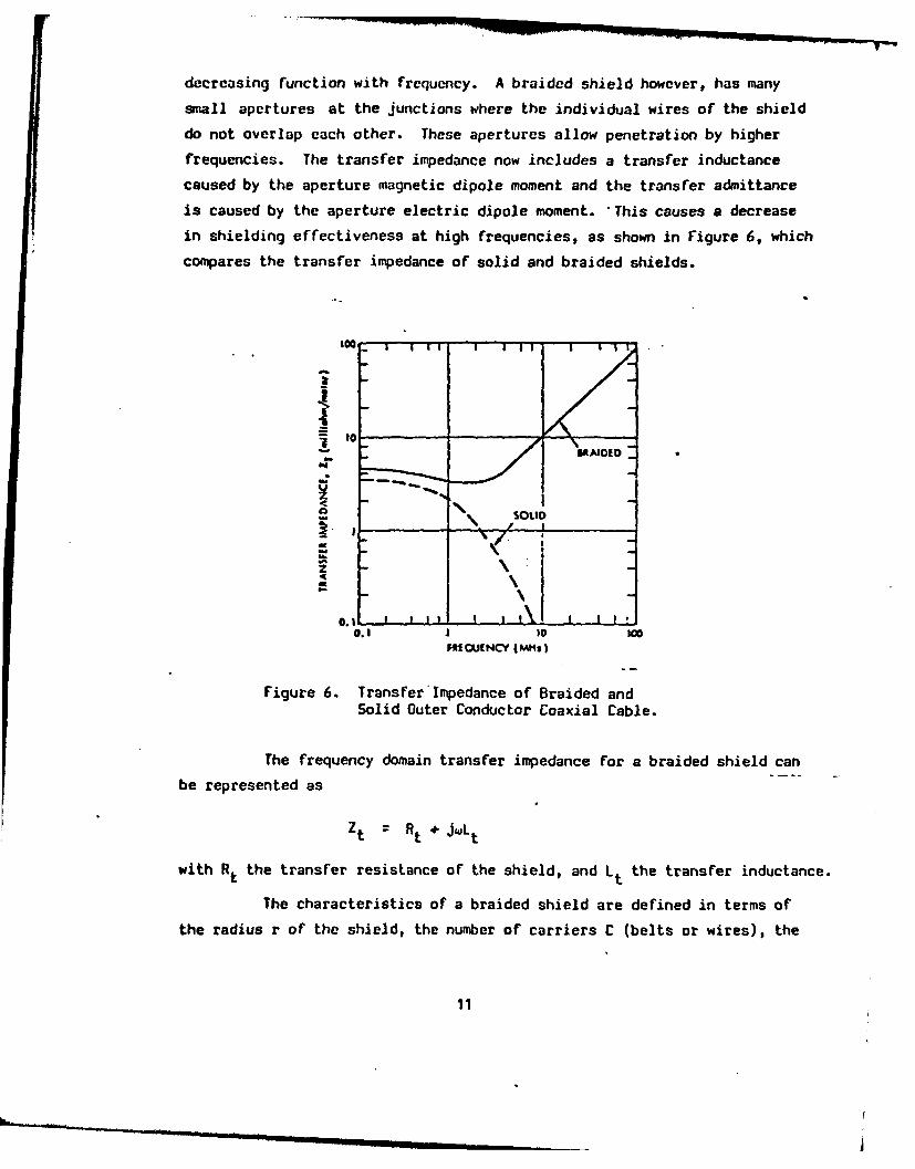
decreasing function with frequency. A braided shield however, has many
small apertures at the junctions where the individual wires of the shield
do not overlap each other. These apertures allow penetration by higher
frequencies. The transfer impedance now includes a transfer inductance
caused by the aperture magnetic dipole moment and the transfer admittance
is caused by the aperture electric dipole moment. *This causes a decrease
in shielding effectiveness at high frequencies, as shown in Figure 6, which
compares the transfer impedance of solid and braided shields.
II
0IJ
SOI
zA
PEE OJCNCY (Mbtz)
Figure 6. TransferImpedance of Braided andSolid Outer Conductor Coaxial Cable.
The frequency domain transfer impedance for a braided shield can
be represented as
t Rt e Lt
with Rt the transfer resistance of the shield, and Lt the transfer inductance.
The characteristics of a braided shield are defined in terms of
the radius r of the shield, the number of carriers C (belts or wires), the
11

picks P (number of carrier crossings per unit length), and ends N (number
of wires in each carrier), and the individual wire diameter d [5].
A typical braided pattern is shown in Figure 7. The pitch angle
. is given by
a = tan 1 a
C
and the coverage of one carrier is
PNdsina
c2wa
4lr
Figure 7. Braided Pattern Developed on a Plane.
IQ
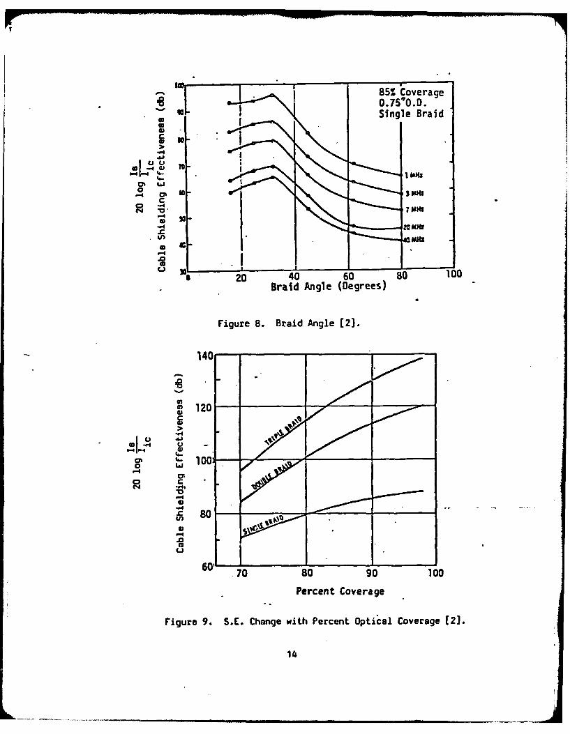
A useful item is the optical coverage of the shield, which is
equal to
K = 2F-F.
Typical braided shields have optical coverages of from 85 to 95 percent and
12
an a of 300 to 450. Figures 8 and 9 show how the different parameters
affect the shielding effectiveness of braided shields, which is defined
by
Cable Shielding 2sEffectiveness" 201og. .
with Is the shield current, and Iic the inner conductor current.
The transfer resistance of the shield is
1 y _dR = 11rdaFcos2 a sinhyd
with
and the transfer inductance is given by
L (1 -K) 3'2 e26C E(e2 )-tan2aK(e)
with
e 2 = 1-tan'a
and K(e) and E(e2) the complete elliptic integral of the first and second
kind.
The transfer admittance is given by
Yt = C CC 7EP1
with C, and C2 the capacitances between the shield and ground, and the shield
and the inner conductor respectively. However, the transfer-admittance dis
so small, that it can usually be iQnored [6].
The cross-sections of two F-18 BTSP cables are shown in Figure 10,
and are arbitrarily labeled BISP #1 and BTSP #2 for easy referencing.
Table 2 shows the parameters calculated for these cables. The transfer
admittance, Yt, is neglibible and is not used further. Therefore, only
13
85% Coverage'S 0.75q0.D.
Single Braid
m~ Li
0
Brai Anl Dges
-4
.0 0
100
0)
o CrC-4
60'
Percent Coverage
Figure 9. S.E. Change with Percent Optical Coverage (2].
14

the shield current drives the inner conductors, and knowledge of the shield
current is sufficient to determine the BTSP responses.
I 0.052" I0.032"
0. 125"
j ~Metal E J DielectricFigure 10. Two BTSP Cables.
15

TABLE 2.
PARAMETERS OF THE TWO BTSP CABLES
BTSP 01 BTSP 02
ZC 107 0 255 n
L - 0.36 PH/m 0.85 PH/m
Cs 31 pf/m 13 pf/m
R a 54 mn/m 36 nW/mics
Cics - 60 pt/m 212 pf/m
Cic't i 60 pf/m 212 pf/m
Cic - 16 pf/m 3 pt//m
L. = 199 nH/m 52 nH/m
L. i2 - 199 nH/m 52 nH/m
L. -" 54 nH/m 0.78 nH/mic'2R = 136 mn/m 28 mn/mIC
K 83 % 85Sa
Lpigtails 0.23 PH 0.22 PH
Zt 54 mn/mtjw3nH/m 36 ma/mrn-jw3nH/m
Y t +jO.43 pf/m +JWO.50 pf/m
Note: The subscript s refers to the shield parameters, and the subscript
ic refers to the two inner conductors.
16

CHAPTER 4
THE OVERALL COUPLING MODEL AND NUMERICAL RESULTS
In Chapter 2, we showed that the coupling path to cables behind
the avionics bay doors can be modelled as a capacitively loaded slot
antenna. In Chapter 3, we discussed the cabling practices and defined
the shielding parameters for the BTSP cables. In Chapter 4, we will now
present the overall combined coupling model and present the numerical
results.
The overall coupling problem is shown pictorially in Figure 11.
The figure shows two electronics boxes, each bonded to the airframe or
skin, -with a wiring harness or bulk cable connecting the twb boxes. The
bulk cable contains 10 or 20 separate cables, including at least one single
BTSP cable. The desired information is the voltage induced on the BTSP
internal wires.
Electonics Boa
Electronics Box ~ Filter Pin Connectors lcoisB-Electronics Box BSCbe
IBTSP CableLoads Bulk Wiring Harness
Inside
Fuselage Surface
Lightning SurfaceCurrent Desi ty Avionics Bay Doors
Figure 11. Pictorial Representation of OVerallCoupling Problem.
17

We also note that the BISP internal wires can be connected to
balanced load; on each end. Another configuration is possible, namely,
that the load may be unbalanced at one end (one wire connected to struc-
ture) .and balanced at the other.
Indicated on the skin are the three avionics bay doors which
have a total of six slots which are normal to the surface current flow.
The analysis procedure is summarized by first determining a
circuit model for the coupling of the lightning induced skin current to
the bulk cable. The result is the sum total bulk current flowing in the
bulk cable wiring harness. The next step is to partition this current
and determine a reasonable estimate of the current on the single BTSP shield.
Then the BTSP shield current is used to determine the electric fields inside
of it by means of the shield transfer impedance. These fields are sources
which drive the internal wires which are solved by a multiconductor TEN
transmission line code (7, Appendix A]. We note that coupling from the
pigtails and exposed terminations is negligible at these frequencies
compared to the other effects.
The slot model follows that of Reference 1, and is summarized
in Figure 12, which shows the duality between a slot in a perfect conductor
and a strip dipole in free space, both of which are small in terms of wave-
length.
erfect Electic Conductor - . .
a. Slot Antenna.
Zdiple
V VO• 2%, Inc
b. Complementary Strip Dipole.
Figure 12. A Slot Antenna and Its Complementary Strip Dipole.
18
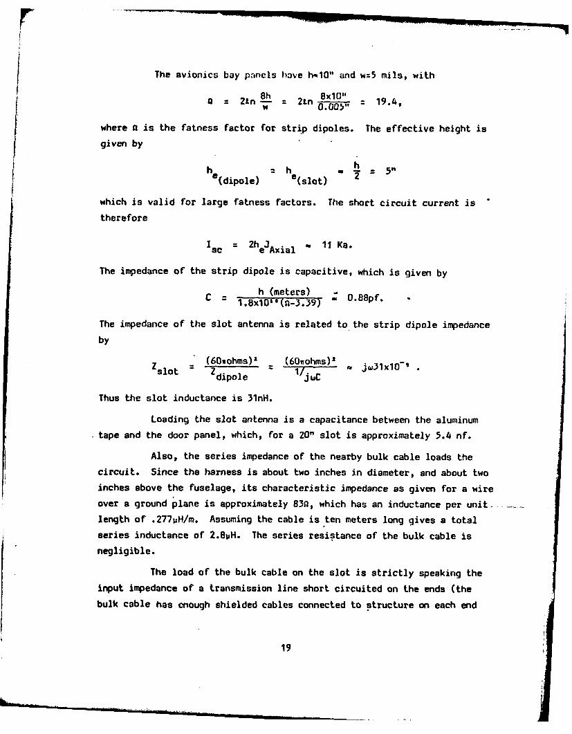
The avionics bay panels have h"10" and w=5 mils, with
=2n8h 8x10"2 =L 2 n =x',, 19.4,w 0.005"
where a is the fatness factor for strip dipoles. The effective height is
given by
he (ih o(dipole) e(slot) 2
which is valid for large fatness factors. The short circuit current is
therefore
Isc = 2he3Axia l 11Ka.
The impedance of the strip dipole is capacitive, which is given by
h (meters) -1.8x101(-3.39) a 0.88pf. -
The impedance of the slot antenna is related to the strip dipole impedance
by
(60wohms)' = (60uohms)2 *3110 'slot = Zdipole 1/JWC
Thus the slot inductance is 31nH.
Loading the slot antenna is a capacitance between the aluminum
tape and the door panel, which, for a 20" slot is approximately 5.4 nf.
Also, the series impedance of the nearby bulk cable loads the
circuit. Since the harness is about two inches in diameter, and about two
inches above the fuselage, its characteristic impedance as given for a wire
over a ground plane is approximately 832, which has an inductance per unit - .
length of .277pH/m. Assuming the cable is ten meters long gives a total
series inductance of 2.8UH. The series resistance of the bulk cable is
negligible.
The load of the bulk cable on the slot is strictly speaking the
input impedance of a transmission line short circuited on the ends (the
bulk cable has enough shielded cables connected to structure on each end
19
to provide low impedamnce terminations). However, because the cable lengths
are very small fractions of a wavelength long, the impedance consists only
of the line inductance, 2.BuH.
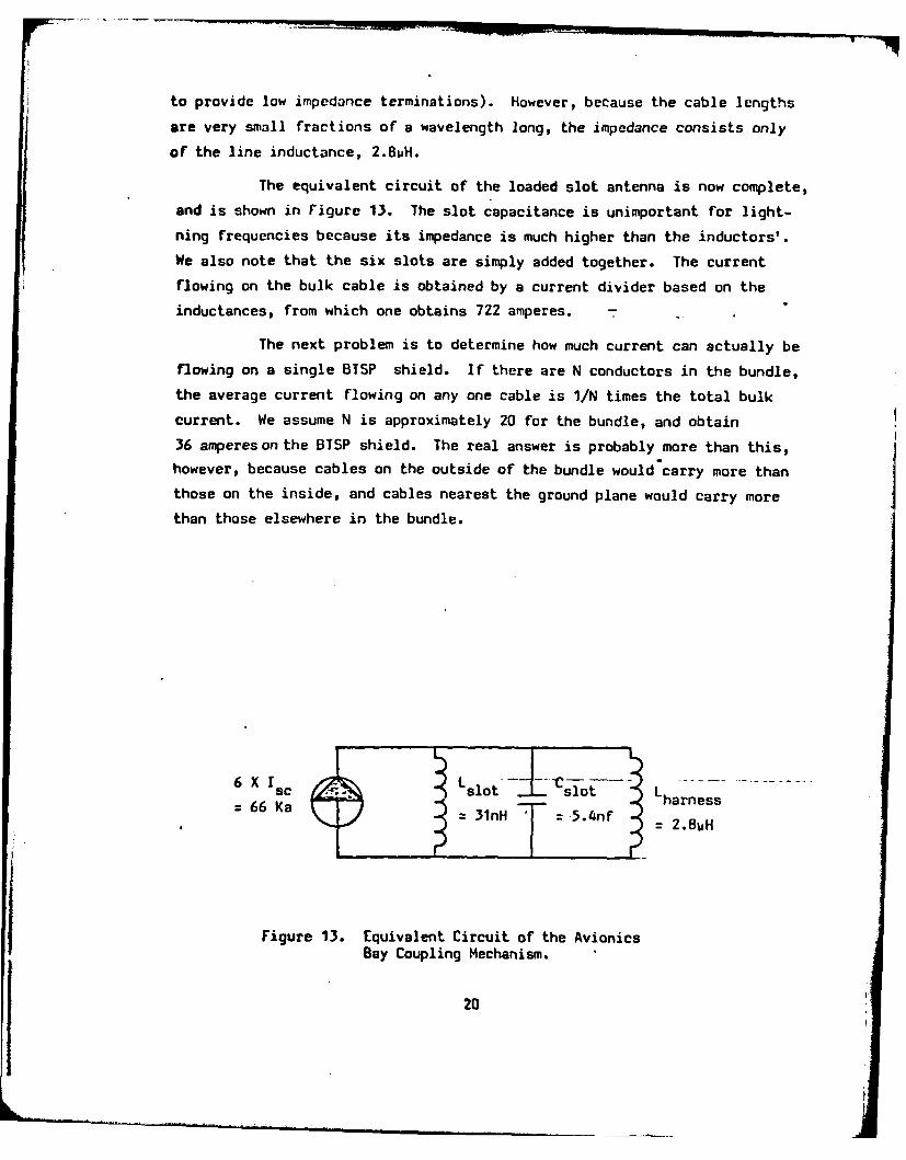
The equivalent circuit of the loaded slot antenna is now complete,
and is shown in Figure 13. The slot capacitance is unimportant for light-
ning frequencies because its impedance is much higher than the inductors'.
We also note that the six slots are simply added together. The current
flowing on the bulk cable is obtained by a current divider based on the
inductances, from which one obtains 722 amperes. -7
The next problem is to determine how much current can actually be
flowing on a single BTSP shield. If there are N conductors in the bundle,
the average current flowing on any one cable is 1/N times the total bulk
current. We assume N is approximately 20 for the bundle, and obtain
36 amperes on the BTSP shield. The real answer is probably more than this,however, because cables on the outside of the bundle would carry more than
those on the inside, and cables nearest the ground plane would carry more
than those elsewhere in the bundle.
66 Ka31nH1 :5.4nf 2.8uH
Figure 13. Equivalent Circuit of the AvionicsBay Coupling Mechanism.
20

In order to obtain an upper bound estimate of the BTSP shield
current, the geometry of Figure 14 was adopted. The BTSP cable is placed
directly under the bulk cable and one insulation thickness away. At
lightning frequencies, the current divides between the two cables according
to
jw(LB+M)
'OTSP IBulk RW+jw(LB+Lw+211)
with
R W - the resistance of the individual wire,
L and LW - the self inductances of the bulk cable and the
single wire, and
F!- the mutual inductance between the bulk cable and
the individual wire.
Again, the resistance of the bulk cable is assumed to be negligible.
All Cables ExceptBTSP
22"
BTSP Cable 211
Ground Plane
Figure 14. Wire Configuration for Worst-Case Current Division.
21
k I I II - I, , _
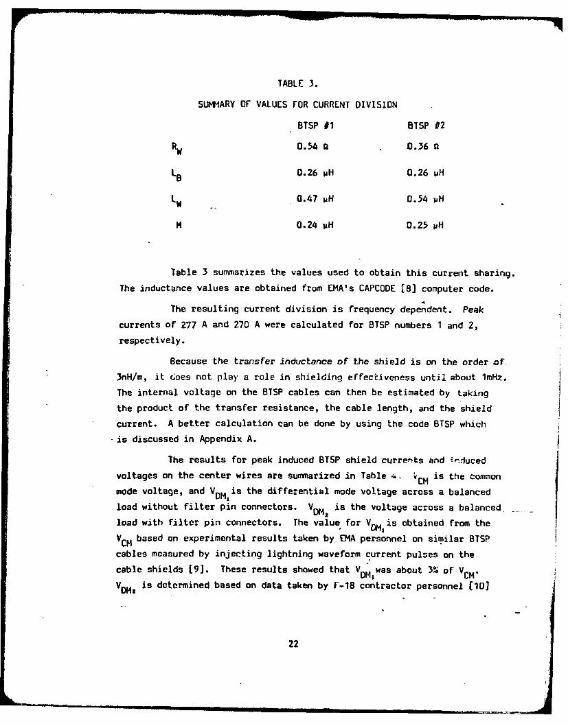
TABLE 3.
SUMMARY OF VALUES FOR CURRENT DIVISION
BTSP #i BISP 02
S.54Q o.36n
LB 0.26 PH 0.26 PH
L 0.47 PH 0.54 uH
M 0.24 PH 0.25 PH
Table 3 summarizes the values used to obtain this current sharing.
The inductance values are obtained from EMA's CAPCODE [8] computer code.
The resulting current division is frequency dependent. Peak
currents of 277 A and 270 A were calculated for BTSP numbers 1 and 2,
respectively.
Because 'the transfer inductance of the shield is on the order of-
3nH/m, it does not play a role in shielding effectiveness until about lmHz.
The internal voltage on the BTSP cables can then be estimated by taking
the product of the transfer resistance, the cable length, and the shield
current. A better calculation can be done by using the code BTSP which
.is discussed in Appendix A.
The results for peak induced BTSP shield currents and induced
voltages on the center wires are summarized in Table , MC is the common
mode voltage, and VDM is the differential mode voltage across a balanced
load without filter pin connectors. VDM, is the voltage across a balanced .
load with filter pin connectors. The value for VDM is obtained from the
VCM based on experimental results taken by EMA personnel on similar BTSP
cables measured by injecting lightning waveform current pulses on the
cable shields (9]. These results showed that VDwas about 3* of VDMI CM*V042 is determined based on data taken by F-18 contractor personnel (10]
22
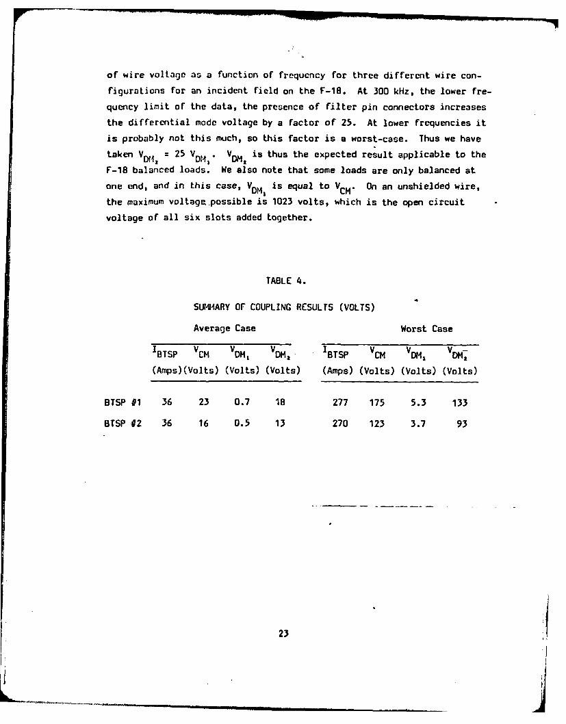
of wire voltage as a function of frequency for three different wire con-
figurations for an incident field on the F-18. At 300 kHz, the lower fre-
quency limit of the data, the presence of filter pin connectors increases
the differential mode voltage by a factor of 25. At lower frequencies it
is probably not this much, so this factor is a worst-case. Thus we have
taken V 25 V VD is thus the expected result applicable to the0fM DM I DMF-18 balanced loads. We also note that some loads are only balanced at
one end, and in this case, VDM, is equal to VCM. On an unshielded wire,
the maximum voltage possible is 1023 volts, which is the open circuit
voltage of all six slots added together.
TABLE 4.
SU14ARY OF COUPLING RESULTS (VOLTS)
Average Case Worst Case
IBTSP VCM VDMI V DM. IBTSP VCM V DM VDM2
(Amps)(Volts) (Volts) (Volts) (Amps) (Volts) (Volts) (Volts)
BTSP #1 36 23 0.7 18 277 175 5.3 133
BTSP #2 36 16 0.5 13 270 123 3.7 93
23
j=

The computed voltage waveforms V for the worst-case division
are given in Figure 15. C
200
~a BISP 01
~BJS 1005
A 100
-50
0 20 40 60 80 100Time (uas)
Figure 15. Induced STSP Common Mode Voltages forWorst-Case Division.
24

CHAPTER 5
SM4ARY AND CONCLUSIONS
The analytical results show that BTSP inner wire common and
differential mode voltages for a worst case lightning stroke are in thenominal range of 16-175 volts and 0.5-5.3 volts, respectively. It is
observed that this worst case stroke occurs much less than 1?0 of all
lightning strokes (Figure 16), and an average value would be approxi-
mately 100 of the above values.
1.00 5V_
WLJ .80 4
Lea .60
.0-
V =.4o A B 2
BJ 2
.20
BX-U
00
Lightning Stroke Current (kiloamps)
Figure 16. Lightning Stroke CurretA Probability Curve.
25
UJ

Several assumptions were made in this analysis:
1. The six slots were assumed to be mutually decoupled.
2. The slot excitation of the bulk cable was assumed to not
depend upon the distance between the cable and the slots.
3. Coupling estimates included the avionics bay doors only;
no other coupling paths were included, and there likely
are some others.
Table 5 summarizes our results for a BTSP cable excited by the
F-18 avionics bay doors. We have also included results for a near-miss
worst-case lightning stroke (50 meters away), which results in 20 of the
surface current of a direct strike. The voltages are similarily scaled.
We point out that the results are based on a linear analysis.
That is to say, a full-threat level lightning stroke may cause arcing to
occur at significant points and change the coupling response. The response
may be either larger or smaller than that predicted by the linear analysis.
Nonlinear effects are quite difficult to predict, and can be accurately
determined only by a threat-level test.
TABLE 5.
SUMMARY OF COUPLING RESULTS FOR 200 KA LIGHTNING STRIKE
Units are volts and are time domain peak values
Direct Stroke Near Miss
V without filter pin . .connectors 0.5-5.3 0.010-0.106
VDM with filter pinconnectors 13-133 0.26-2.7
26

REFERENCES
1. D. E. Merewether, et. al, Electromagnetic Pulse Handbook for Misslesand Aircraft in Flight, SC-M-710346, Sandia Laboratories, Sept. 1972.
2. R. A. Perala and T. F. Ezell, Engineering Design Guidelines for EMPHardening of Naval Missiles and Airplanes, AHIRC-R-17, Mission ResearchCorporation, Dec. 1973.
3. K. M. Lee, R. A. Perala, and R. B. Cook, Induced Effects of Lightningon the Advanced Design Composite Aircraft, AHRC-R-137, Mission ResearchCorporation, July 1978.
4. D. Strawe and L. Piszker, Interaction of Advanced Composites withElectromagnetic Pulse (EMP) Environment, AFML-TR-75-141, BoeingAerospace Company, Sept. 1975.
5. E. F. Vance, ShieIding Effectiveness of Braided Wire Shields, Inter-action Note 172, April 1974.
6. D. E. Merewether and T. F. Ezell, The Effect of Mutual Inductance andMutual Capacitance on the Transient Response of Braided-Shield CoaxialCables, IEEE Trans. EMC, Feb. 1976.
7. R. A. Perala, Excitation Functions for Multiconductor TransmissionLines Illumined by Nonuniform Electromagnetic Fields, AMRC-R-24Mission Research Corporation, June 1974.
8. L. Licking, Capacitance Analysis for Arbitrary Cylindrical Geometries;Aplication to Electromagnetic Coupling into Subsystems Through Cables,SC-RR-72-0299, Sandia Laboratories, May 1972.
9. R. A. Perala, R. B. Cook, and 3. D. Robb, Support of Lightning Analysisand Testing on the Solid Rocket Booster (SRB) Vehicle, AMRC-R-122,Mission Research Corporation, March 1978.
10. G. Weinstock, Viewgraphs presented at NAVAIR, on 5 March, 1979, McDonnellAircraft Company, St. Louis, Missouri.-
27
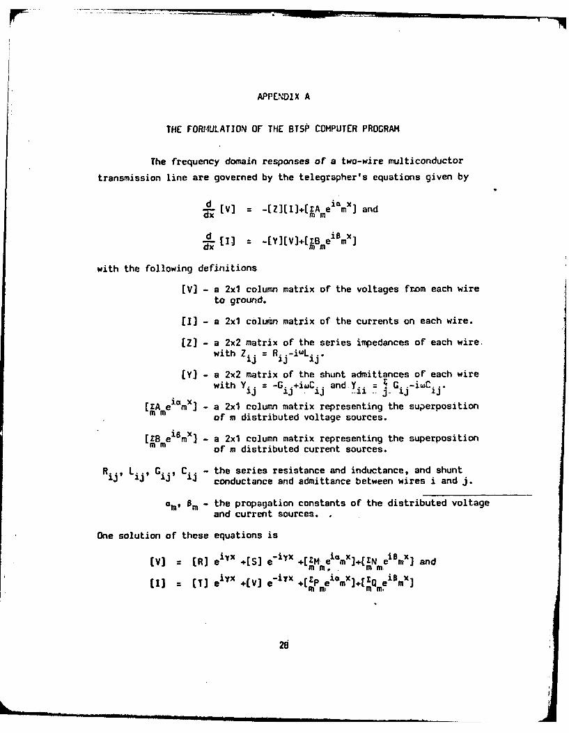
APPENDIX A
THE FORMULATION OF THE BTSP COMPUTER PROGRAM
The frequency domain responses of a two-wire multiconductor
transmission line are governed by the telegrapher's equations given by
d (V = -[Z][I]+[ZAeia mX] and
d [I] = -[Y]([v+[EB eismxdx m m
with the following definitions
(V] - a 2x column matrix of the voltages from each wireto ground.
[1] - a 2x1 column matrix of the currents on each wire.
[Z] - a 2x2 matrix of the series impedances of each wire.with Zij = Rij-iwLij.
[Y] - a 2x2 matrix of the shunt admittances of each wirewith Yi -G. +iWC. and Y.i = 4_. -iWC"
CIAmel mx] - a 2x column matrix representing the superpositionm mof m distributed voltage sources.
[ZBmei. m x ] - a 2x1 column matrix representing the superpositionm mof m distributed current sources.
R.., Li, Gi, C. - the series resistance and inductance, and shuntj 13 conductance and admittance between wires i and j.
a., 0. - the propagation constants of the distributed voltageand current sources.
One solution of these equations is
[V] = (R] eix +S] e-ix +ZM eimX]+(ZN elmx] andmm.. mm
(1] (T] ei Y X +(V] e-iTx +CZ lamx+EQ e is m x: +[mmem +mm.
28

with
(R] - a 2x row matrix representing the amplitudes ofthe forward traveling voltage wave.
CS] - a 2x1 row matrix representing the amplitudes ofthe backward.traveling voltage wave.
(UM eIQmX] - a Zxl column matrix representing the superpositionm m. of the voltage responses from the voltage sources.
[EN e imXJx - a 2x1 column matrix representing the superpositionm M. of the voltage responses from the current sources.
IT]- a 2x row matrix representing the amplitudes ofthe forward traveling current wave.
[V] - a 2x row matrix representing the amplitudes ofthe backward traveling current wave.
[rPmeo m'x]m - a 2x1 column matrix representing the superpositionof the current responses from the voltage sources.
( e im] - a 2x column matrix representing the superpositionm m of the current responses from the current sources.
iYxe - a scalar representing a forward traveling wave.
eiy - a scalar representing a backward traveling wave.
y - the propagation constant of the wires (both wires are
assumed to have the same propagation constant).
The homogeneous solution gives the following relationships
(T] =L [YJ[R] and [U] - [Y](S]ly ly
Furthermore, if we define
[G] = (Z(Y]
then 2 = -Z,,Y,,, for a single-wire becomes,
y j 2 2,-1- for two wires.2
The particular solution gives the following for the mth source
jM]1 -m(i11 [[A m]1 mJ = ] 1 ]] and
[ N . ]] ( i m ] Z ] ] " 1 [ O]1
QMU : [ Y] [ism Bm
29

with the following definitions for a two-wire line,
[m]: [t.ll (Nm] [Naml [Pm] = [Pam 1 [Qm] = [om and
L'"'mJ ' L",,,j ' LPImJ LQ~mj
(is] ro, 1 i I, ri01 01 r[A] [Aim] , and [Bm]: [B m1Lm i;2mJ ' o iS'mJ ' LAmJ ' LB:mi
The boundary conditions are applied next, with impedances at
the ends between the two wires and between each wire and ground. Addition-
ally, each impedance to ground is in series with a voltage source. For a
cable bf length L, the boundary conditions are represented as
IVIx=° = [X][Vs]+[CIIIx=° and
[Vlx=L = [W][VLJ+[D[I]x=L
with
[C] - ' a 2x2 matrix with Cii = - andCij -Z 'j j zs..j1
(0]- -a W matrix with D.. =and D -1j Z ij-Z
C..j[X] a 2x2 matrix with X ij
O..i
[W] a 2x2 matrix with W.
[V ] - a 2x1 column matrix of voltage sources on one end ofthe cable,
[VL ] - a 2x1 column matrix of voltage sources on the otherend of the cable,
Z - the impedance between the i and j wires on one end of1j the cable,
and ZL - the impedance between the i and j wires on the other'ij end of the cable.
30
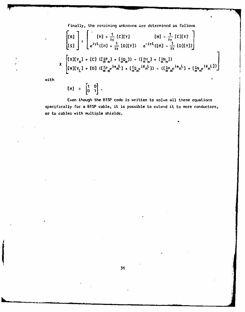
Finally, the rcrnaining unknowns are determined as follows
(RI CH] - (cj(y] 1" CIY41 iYCiy(
R] [H ( c]YH] - [cJ[yJ
s e rL([H] + .- [DI[YJ) ([HI -I- (D][YJ)J
[X][Vs]( + [C] ([1PI + I ZO ()E- ([ ZM I + [N ]) )
,[W)VL +(D] (lEPme imL] +[ L ic L + iS L),~~ ~ M m m ) - ( m m ] m me m
with
CH] = 1(" 10
Even though the BTSP code is written to solve all these equations
specifically for a BTSP cable, it is possible to extend it to more conductors,
or to cables with multiple shields.
I3 31 !

DI
1f