Embed Size (px)
Citation preview

ELEC 3509 Fall 2014
Lab Orientation
http://imgs.xkcd.com/comics/circuit_diagram.png
• Course Information• Lab Information• Guidelines• Schedule• Expectations• Pre-Labs• Lab Reports• Mark Disputes• Tips & Tricks

ELEC 3509 – Fall 2014• Norman Fong (head TA)
– 3303 Canal Building– [email protected]
• Course website– http://www.doe.carleton.ca/~jrogers
• Course Notes + Lab manual
• Lab website– http://www.doe.carleton.ca/~nofong/ELEC3509
• Lab guidelines (important!)• Marking schemes• Check this website at least once before each lab
• Lab content– Design, simulation, building and testing of analog circuits and devices– Labs start Tuesday September 23rd

Lab Schedule• Room: 4195
Mackenzie• You must attend your
registered section• Show up on time! • TAs have been
instructed to not stay later than the assigned lab hours
• You can also work on your own anytime the lab is open
Due to the high enrollment in both this course and ELEC 2501, it is unlikely that there will be extra space during another section so those students will be given priority.
Lab Guidelines• Labs are every week and performed in groups of 2• Worth 30% of your final mark• You MUST pass the lab in order to pass the course• One report is to be submitted per group. Both students will receive the same mark.• You MUST hand in a satisfactory report for every lab
– You cannot submit an unfinished report (missing large portions, no results etc.)• Every lab will have a marked prelab
– Marked on an all-or-nothing basis• Every lab will have a marked checkout
– Your lab must be complete on time and in your designated lab section– It is your responsibility to be done on time
• If you are knowingly going to miss a lab contact your TA prior to the lab– We can arrange an alternate lab day for you to attend without lateness penalty– Missed labs due to illness will require a doctor’s note.
Plagiarism
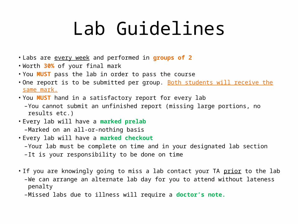
• Zero tolerance!– Automatic mark of zero for all parties– Report to the Professor and sent to the Dean– http://www1.carleton.ca/studentaffairs/academic-integrity/
• Last year (2013 Fall) we had 30 (!!!) students with suspicious reports for Lab 2 – Most of these reports were sent to the Dean
• What constitutes plagiarism?– Copying any content (text, figures, tables, data) from any source
• This includes your own work from previous years
– Failing to acknowledge sources through citations

Lab Expectations
• Read over the lab before showing up• Walk through the lab and understand what you are going to be
doing• E-mail a TA to ask a question of something is unclear• Pro tip: If possible, pre-assemble your circuits and setup Excel or
Matlab files
• Complete the pre-lab before entering• Be able to debug your circuits on your own before
calling a TA• Manage your time effectively• Clean up your station after you are done

Pre-labs• Every lab has a marked prelab, including Lab 1!• The pre-labs are all extensive and typically include all of your design
calculations– You won’t be able to do the labs without them!– Treat them like you would an assignment– Pre-labs for labs 2,3 and 4 can take several hours (more likely days) to
complete.• Prelabs will be checked at the beginning of the lab (first 30 mins)• We will ask you technical questions about the pre-lab to verify that
it was not simply copied from someone else.• Marks are all or nothing• If your prelab is not ready at the start of the lab, TAs will not help
you complete it during the lab.

Lab Kits
• The lab manager will distribute lab kits which include:– A breadboard and all the components you will
need for these labs– One kit is required per group at a cost of $15– If you already have your own equipment then you
can use that instead.

Lab Reports• Reports are due one week after the lab has been completed • They are due 30 minutes after the beginning of your lab session• Drop off in stairwell drop boxes outside 41xxME.• Late reports will lose 25% immediately and 10% PER DAY after.
• If you are knowingly submitting your lab late, contact Norm immediately and an electronic submission may be accepted.
• It is ultimately YOUR responsibility to have your lab in on time.

How to Write a “Good” Lab Report• There is no specified format, however it should be logically organized and
written in a professional manner• The following is an example of how you could organize a design report:
– Introduction• Explain what you are doing and how you will be doing it
– Specifications• Explain the design specifications of the lab.
– Design• Organize the calculations from your pre-lab and explain your design.• This is incredibly important. Just showing equations is not sufficient. You must explain what you are doing
with these equations as well as the results.
– Testing/Results• Explain how the circuit was implemented.• Explain the order in which measurements were taken and show the results• Explain conclusions derived from these results• Compare results to predicted results
– Summary• Summarize key results and provide a conclusion
– References• Reference materials or figures properly• IEEE citation format: http://www.ieee.org/documents/ieeecitationref.pdf

How to Write a “Good” Lab Report• Your lab report should:
– Be thorough and concise– Be readable without having prior knowledge of the lab– Describe what you did and how you did it– Explain and discuss the results– Have all figures and plots labelled with appropriate units– Cover everything in the marking scheme
Prove that you did the work and understood it.
• You will not be given the benefit of the doubt if your report is vague or unclear
• Stay in contact with your lab partner to make sure everything is done on time

Common Lab Report Mistakes
• Failing to verify that all marking scheme requirements are addressed in the body of the report
• Failing to re-develop the design equations in the body of the report – Just attaching the pre-lab as an appendix is insufficient, you must
use an equation editor to include the design equations in the body of your report
• Failing to refer to figures and tables in the text of the report • Failing to compare expected and observed results & propose
explanations for the variation • Failing to check for spelling and grammar errors before
submitting

Mark Disputes• Lab Report Returns
– We will try to return your labs 1 week after they are submitted
• Mark Disputes– If you wish to dispute a mark, you must do the following
• Wait 24 hours and review the marking scheme for the lab• Send the marking TA e-mail with an explanation as to why you think you deserve a
different mark. • If this cannot be resolved then you should request a meeting
• TAs are instructed to NOT give out additional marks just because a student complains. Justification is required.
• TAs will not adjust your mark in lab (so don’t ask)

Lab CalendarLab 1: BJT DC and AC Characteristics (2 weeks)Lab 2: Two transistor amplifier project (3 weeks)Lab 3: 741-Op Amp (2 weeks)Lab 4: Active bandpass filter (2 weeks)Lab 5: Oscillator (1 week, no report)

Lab Tips: Breadboard• Lab kits will be distributed during the first lab
– Breadboard, components, etc.– Find a convenient carrying case
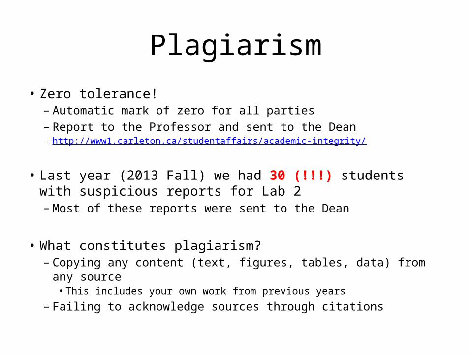
• Familiarize yourself with the breadboard• Utilize the upper and lower “rails” for your power supplies
Lab Tips: Power Rails
Bad IdeaGood idea
VCC=15V

Lab Tips: Circuit Layout
+-
Try to lay out your devices to match the circuit diagram.
Intelligently place your transistors, resistors and chips.
Use short jumper cables instead of stretching out the pins on your device.

Lab Tips: Electrolytic Capacitors
• Electrolytic capacitors are directional• Ensure polarity is properly aligned in your
circuit– They can blow up if placed improperly
The arrow points in the direction of current flow (i.e. The negative terminal)
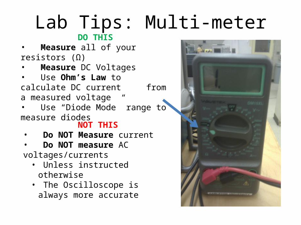
Lab Tips: Multi-meterDO THIS
• Measure all of your resistors (Ω)• Measure DC Voltages • Use Ohm’s Law to calculate DC current from a measured voltage• Use “Diode Mode” range to measure diodes
NOT THIS• Do NOT Measure current• Do NOT measure AC voltages/currents• Unless instructed otherwise• The Oscilloscope is always more
accurate

Lab Tips: Oscilloscope Prob
e tip
Ground
•The probe does not have positive or negative terminals • Ground must always be connected to ground• “Autoset” is not your friend!• Can be used to initially capture a signal but if you press it again it
will reset all of your settings• Measure peak-to-peak voltages using the cursors• Do not trust the digital “measure” function, especially if the signal is noisy
Cursor Buttons
Autoset – Resist the urge to spam this button

Tips & Tricks: Equation Editors
• Use an Equation Editor so that the TAs can read your work– Hand-written pre-labs attached at the end of the report are not
acceptable!
• MS Word 2010 has a built-in equation editor (see below)• Other equation editors you might consider are:
– Maple (on DOE computers)– LaTex (online)
Pro Tip: How to find the Equation Editor in MS Word 2010

END

Lab Tips• A potentiometer is a 3 terminal variable resistor which acts as a voltage divider.• You do not need to add another 1kΩ resistor to your circuit. The potentiometer is the resistor.