Embed Size (px)
Citation preview

3-140
Eight Character 5 mm and 7 mmSmart Alphanumeric Displays
Technical Data
Features• X Stackable (HDSP-21XX)• XY Stackable (HDSP-250X)• 128 Character ASCII
Decoder• Programmable Functions• 16 User Definable
Characters• Multi-Level Dimming and
Blanking• TTL Compatible CMOS IC• Wave Solderable
Applications• Computer Peripherals• Industrial Instrumentation• Medical Equipment• Portable Data Entry Devices• Cellular Phones
• TelecommunicationsEquipment
• Test Equipment
DescriptionThe HDSP-210X/-211X/-250Xseries of products is ideal forapplications where displayingeight or more characters of dotmatrix information in anaesthetically pleasing manner isrequired. These devices are8-digit, 5 x 7 dot matrix, alpha-numeric displays and are allpackaged in a standard 15.24 mm(0.6 inch) 28 pin DIP. The on-board CMOS IC has the ability todecode 128 ASCII characterswhich are permanently stored inROM. In addition, 16 program-mable symbols may be stored inon-board ROM, allowing consider-
HDSP-210X SeriesHDSP-211X SeriesHDSP-250X Series
able flexibility for displayingadditional symbols and icons.Seven brightness levels provideversatility in adjusting the displayintensity and power consumption.The HDSP-210X/-211X/-250Xproducts are designed forstandard microprocessor interfacetechniques. The display andspecial features are accessedthrough a bidirectional 8-bit databus.
Device Selection Guide
AlGaAs High EfficiencyFont Height Red Red Orange Yellow Green
0.2 inches HDSP-2107 HDSP-2112 HDSP-2110 HDSP-2111 HDSP-2113
0.27 inches – HDSP-2502 HDSP-2500 HDSP-2501 HDSP-2503
H
5964-6378E

3-141
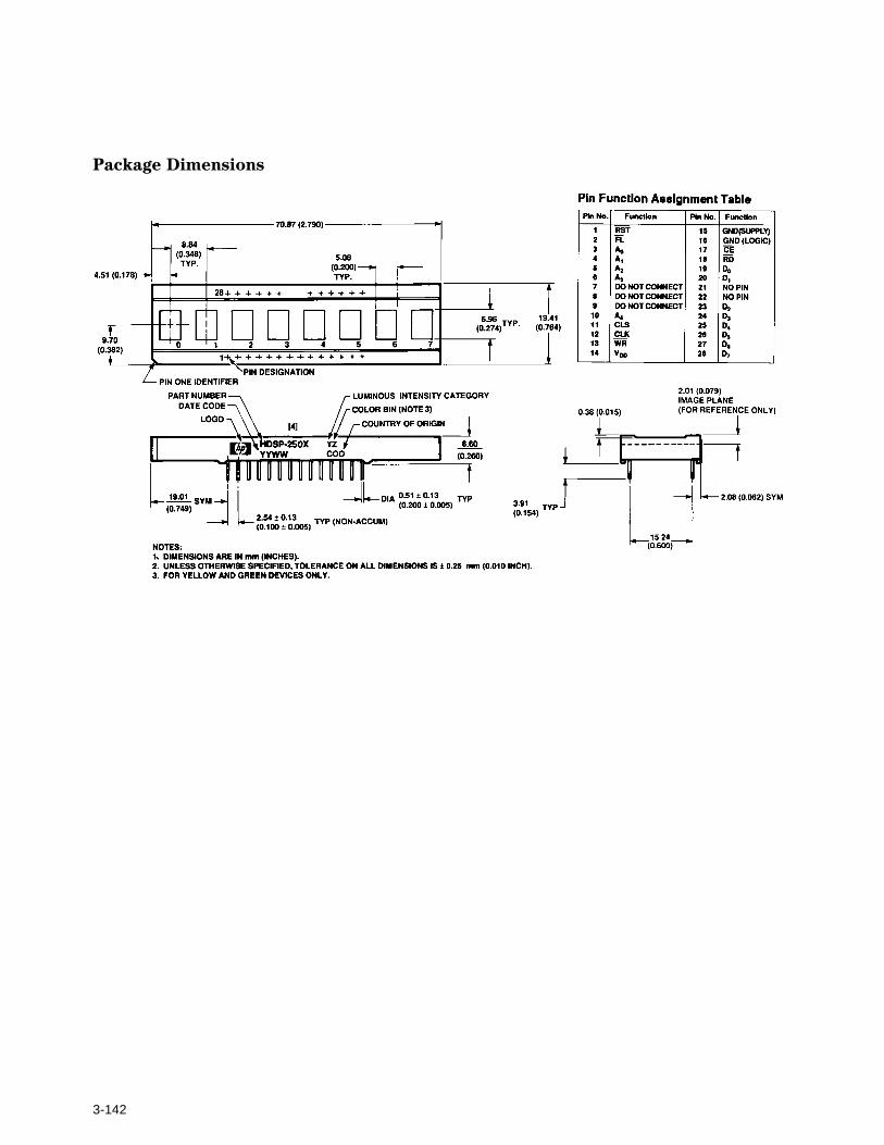
Package Dimensions
ESD WARNING: STANDARD CMOS HANDLING PRECAUTIONS SHOULD BE OBSERVED TO AVOIDSTATIC DISCHARGE.
Absolute Maximum RatingsSupply Voltage, VDD to Ground[1] ........................................ -0.3 to 7.0 VOperating Voltage, VDD to Ground[2] ............................................. 5.5 VInput Voltage, Any Pin to Ground ............................. -0.3 to VDD +0.3 VFree Air Operating Temperature Range, TA
[3] ................ -45°C to +85°CStorage Temperature Range, TS ................................... -55°C to +100°CRelative Humidity (non-condensing) ............................................... 85%Maximum Solder Temperature (Below Seating Plane), t < 5 sec .............................................. 260°CESD Protection @ 1.5 kΩ, 100 pF......................... VZ = 4 kV (each pin)Notes:1. Maximum Voltage is with no LEDs illuminated.2. 20 dots ON in all locations at full brightness.3. Maximum supply voltage is 5.25 V for operation above 70°C.
3-142
Package Dimensions

3-143
ASCII Character Set HDSP-210X, HDSP-211X, HDSP-250X Series
Recommended Operating Conditions
Parameter Symbol Minimum Nominal Maximum Units
Supply Voltage VDD 4.5 5.0 5.5 V

3-144
Electrical Characteristics over Operating Temperature Range (-45°C to +85°C)4.5 V < VDD < 5.5 V, unless otherwise specified
TA = 25°C -45°C < TA < + 85°C VDD = 5.0 V 4.5 V < VDD < 5.5 V
Parameter Symbol Typ. Max. Min. Max. Units Test Conditions
Input Leakage IIH 1.0 µA VIN = 0 to VDD,(Input without pullup) IIL -1.0 pins CLK, D0-D7,
A0-A4
Input Current IIPL -11 -18 -30 µA VIN = 0 to VDD,(Input with pullup) pins CLS, RST,
WR, RD, CE, FL
IDD Blank IDD (BLK) 0.5 3.0 4.0 mA VIN = VDD
IDD 8 digits IDD(V) 200 255 330 mA “V” on in all 812 dots/character[1,2] locations
IDD 8 digits IDD(#) 300 370 430 mA “#” on in all20 dots/character[1,2,3,4] locations
Input Voltage High VIH 2.0 VDD V+0.3
Input Voltage Low VIL GND 0.8 V-0.3 V
Output Voltage High VOH 2.4 V VDD = 4.5 V,IOH = -40 µA
Output Voltage Low VOL 0.4 V VDD = 4.5 V,D0-D7 IOL = 1.6 mA
Output Voltage Low VOL 0.4 V VDD = 4.5 V,CLK IOL = 40 µA
High Level Output IOH -60 mA VDD = 5.0 VCurrent
Low Level Output IOL 50 mA VDD = 5.0 VCurrent
Thermal Resistance RθJ-C 15 °C/WIC Junction-to-Case
Notes:1. Average IDD measured at full brightness. See Table 2 in Control Word Section for IDD at lower brightness levels. Peak
IDD = 28/15 x IDD (#).2. Maximum IDD occurs at -55°C.3. Maximum IDD(#) = 355 mA at VDD = 5.25 V and IC TJ = 150°C.4. Maximum IDD(#) = 375 mA at VDD = 5.5 V and IC TJ = 150°C.

3-145
Optical Characteristics at 25°CVDD = 5.0 V at Full Brightness
Luminous Intensity Peak DominantCharacter Average (#) Wavelength Wavelength
Part Iv (mcd) λPeak λdDescription Number Min. Typ. (nm) (nm)AlGaAs HDSP-2107 5.0 15.0 645 637HER HDSP-2112 2.5 7.5 635 626
-2502Orange HDSP-2110 2.5 7.5 600 602
-2500Yellow HDSP-2111 2.5 7.5 583 585
-2501High HDSP-2113 2.5 7.5 568 574Performance -2503Green
Note: 1. Refers to the initial case temperature of the device immediately prior to measurement.
[1]
AC Timing Characteristics over Temperature Range (-45°C to +85°C)4.5 V < VDD < 5.5 V, unless otherwise specified
ReferenceNumber Symbol Description Min.[1] Units
1 tACC Display Access Time Write 210 Read 230 ns
2 tACS Address Setup Time to Chip Enable 10 ns3 tCE Chip Enable Active Time[2,3]
Write 140 Read 160 ns
4 tACH Address Hold Time to Chip Enable 20 ns5 tCER Chip Enable Recovery Time 60 ns6 tCES Chip Enable Active Prior to Rising Edge of [2,3]
Write 140 Read 160 ns
7 tCEH Chip Enable Hold Time to Rising Edge ofRead/Write Signal[2,3] 0 ns
8 tW Write Active Time 100 ns9 tWSU Data Write Setup Time 50 ns10 tWH Data Write Hold Time 20 ns11 tR Chip Enable Active Prior to Valid Data 160 ns12 tRD Read Active Prior to Valid Data 75 ns13 tDF Read Data Float Delay 10 ns
tRC Reset Active Time[4] 300 ns
Notes:1. Worst case values occur at an IC junction temperature of 150° C.2. For designers who do not need to read from the display, the Read line can be tied to VDD and the Write and Chip Enable lines can be
tied together.3. Changing the logic levels of the Address lines when CE = “0” may cause erroneous data to be entered into the Character RAM,
regardless of the logic levels of the WR and RD lines.4. The display must not be accessed until after 3 clock pulses (110 µs min. using the internal refresh clock) after the rising edge of the
reset line.

3-146
AC Timing Characteristics over Temperature Range (-45°C to +85°C)4.5 V < VDD < 5.5 V, unless otherwise specified
Write Cycle Timing Diagram
Symbol Description 25°C Typ. Min.[1] Units
FOSC Oscillator Frequency 57 28 kHz
FRF[2] Display Refresh Rate 256 128 Hz
FFL[3] Character Flash Rate 2 1 Hz
tST[4] Self Test Cycle Time 4.6 9.2 sec
Notes:1. Worst case values occur at an IC junction temperature of 150°C.2. FRF = FOSC/2243. FFL = FOSC/28,6724. tST = 262,144/FOSC
3-147
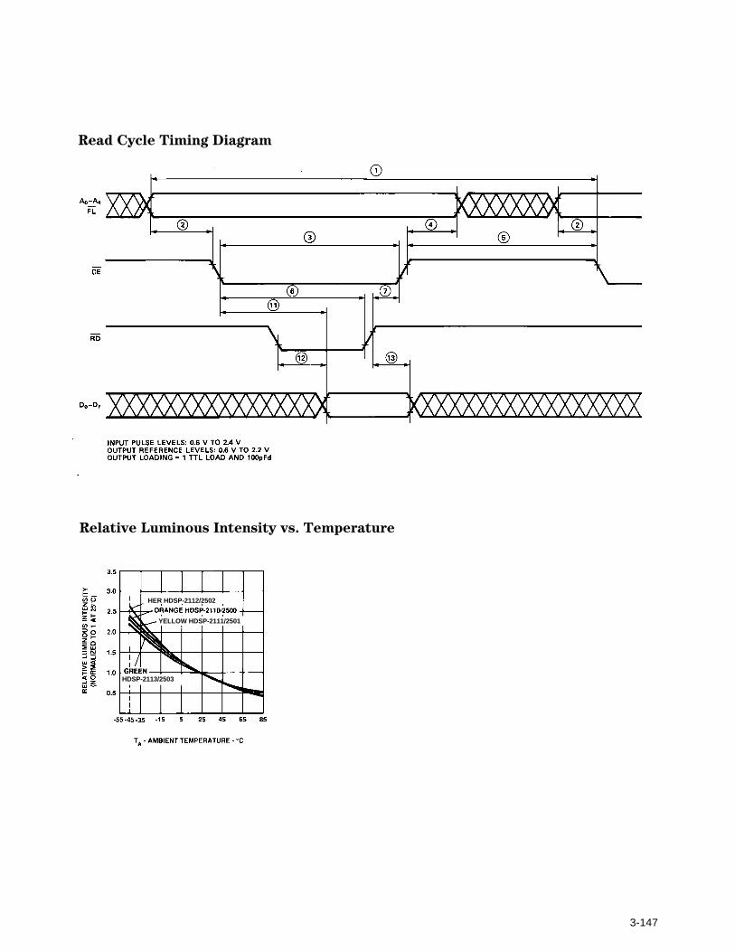
Read Cycle Timing Diagram
Relative Luminous Intensity vs. Temperature
HER HDSP-2112/2502
HDSP-2113/2503
YELLOW HDSP-2111/2501
3-148
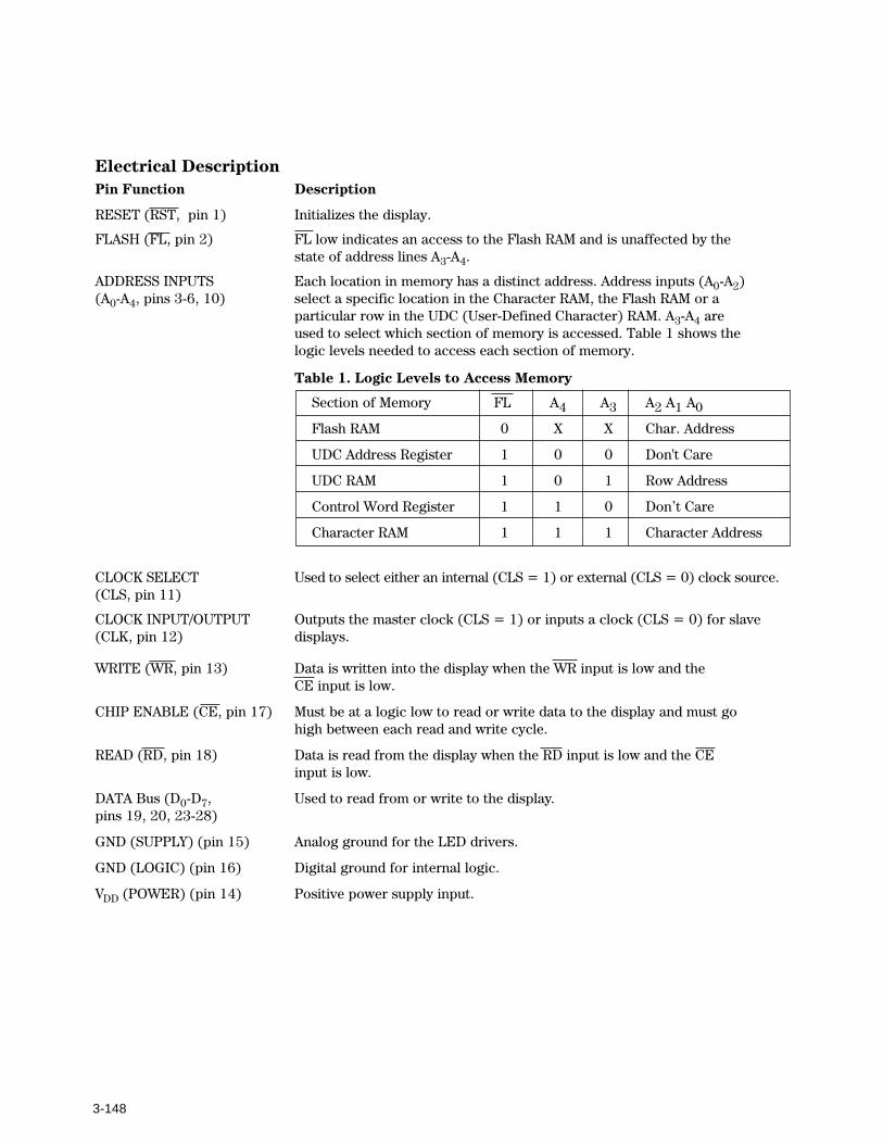
Electrical DescriptionPin Function Description
RESET (RST, pin 1) Initializes the display.
FLASH (FL, pin 2) FL low indicates an access to the Flash RAM and is unaffected by thestate of address lines A3-A4.
ADDRESS INPUTS Each location in memory has a distinct address. Address inputs (A0-A2)(A0-A4, pins 3-6, 10) select a specific location in the Character RAM, the Flash RAM or a
particular row in the UDC (User-Defined Character) RAM. A3-A4 areused to select which section of memory is accessed. Table 1 shows thelogic levels needed to access each section of memory.
Table 1. Logic Levels to Access Memory
Section of Memory FL A4 A3 A2 A1 A0
Flash RAM 0 X X Char. Address
UDC Address Register 1 0 0 Don't Care
UDC RAM 1 0 1 Row Address
Control Word Register 1 1 0 Don’t Care
Character RAM 1 1 1 Character Address
CLOCK SELECT Used to select either an internal (CLS = 1) or external (CLS = 0) clock source.(CLS, pin 11)
CLOCK INPUT/OUTPUT Outputs the master clock (CLS = 1) or inputs a clock (CLS = 0) for slave(CLK, pin 12) displays.
WRITE (WR, pin 13) Data is written into the display when the WR input is low and theCE input is low.
CHIP ENABLE (CE, pin 17) Must be at a logic low to read or write data to the display and must gohigh between each read and write cycle.
READ (RD, pin 18) Data is read from the display when the RD input is low and the CEinput is low.
DATA Bus (D0-D7, Used to read from or write to the display.pins 19, 20, 23-28)
GND (SUPPLY) (pin 15) Analog ground for the LED drivers.
GND (LOGIC) (pin 16) Digital ground for internal logic.
VDD (POWER) (pin 14) Positive power supply input.

3-149
Figure 1. HDSP-210X/-211X/-212X/-250X Internal Block Diagram.
3-150
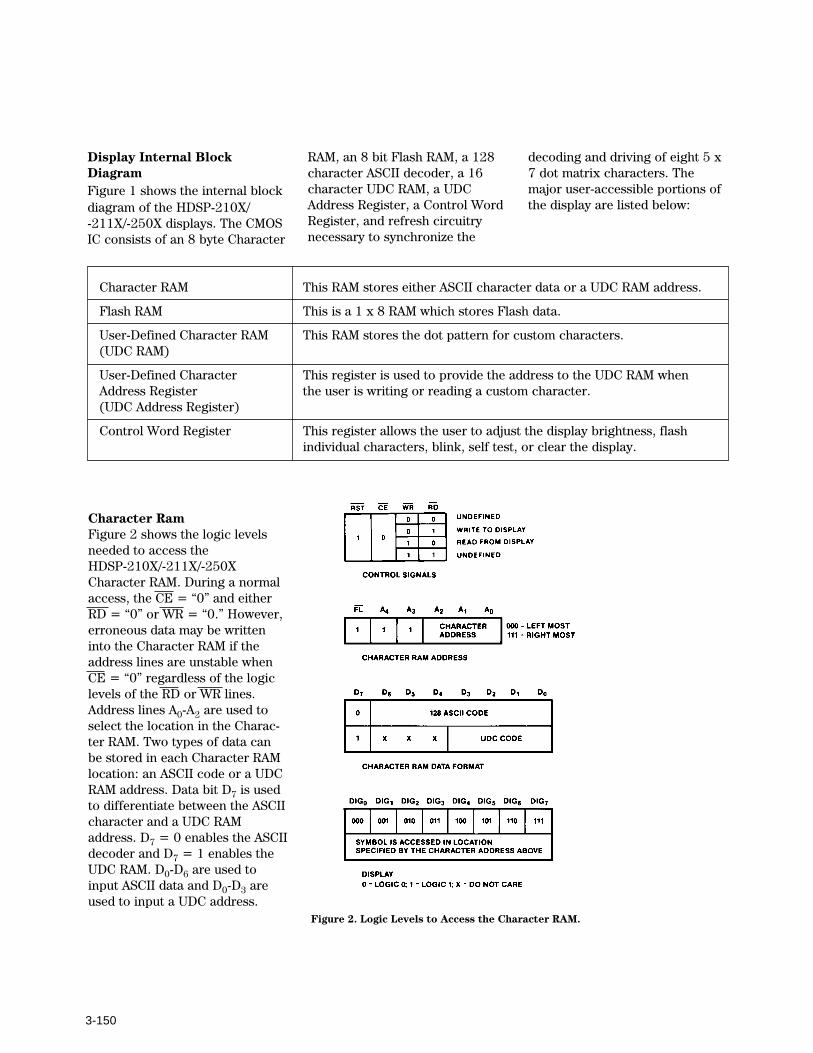
Character RAM This RAM stores either ASCII character data or a UDC RAM address.
Flash RAM This is a 1 x 8 RAM which stores Flash data.
User-Defined Character RAM This RAM stores the dot pattern for custom characters.(UDC RAM)
User-Defined Character This register is used to provide the address to the UDC RAM whenAddress Register the user is writing or reading a custom character.(UDC Address Register)
Control Word Register This register allows the user to adjust the display brightness, flashindividual characters, blink, self test, or clear the display.
Display Internal BlockDiagramFigure 1 shows the internal blockdiagram of the HDSP-210X/-211X/-250X displays. The CMOSIC consists of an 8 byte Character
RAM, an 8 bit Flash RAM, a 128character ASCII decoder, a 16character UDC RAM, a UDCAddress Register, a Control WordRegister, and refresh circuitrynecessary to synchronize the
decoding and driving of eight 5 x7 dot matrix characters. Themajor user-accessible portions ofthe display are listed below:
Character RamFigure 2 shows the logic levelsneeded to access theHDSP-210X/-211X/-250XCharacter RAM. During a normalaccess, the CE = “0” and eitherRD = “0” or WR = “0.” However,erroneous data may be writteninto the Character RAM if theaddress lines are unstable whenCE = “0” regardless of the logiclevels of the RD or WR lines.Address lines A0-A2 are used toselect the location in the Charac-ter RAM. Two types of data canbe stored in each Character RAMlocation: an ASCII code or a UDCRAM address. Data bit D7 is usedto differentiate between the ASCIIcharacter and a UDC RAMaddress. D7 = 0 enables the ASCIIdecoder and D7 = 1 enables theUDC RAM. D0-D6 are used toinput ASCII data and D0-D3 areused to input a UDC address.
Figure 2. Logic Levels to Access the Character RAM.

3-151
UDC RAM and UDC AddressRegisterFigure 3 shows the logic levelsneeded to access the UDC RAMand the UDC Address Register.The UDC Address Register iseight bits wide. The lower fourbits (D0-D3) are used to select oneof the 16 UDC locations. Theupper four bits (D4-D7) are notused. Once the UDC address hasbeen stored in the UDC AddressRegister, the UDC RAM can beaccessed.
To completely specify a 5 x 7character, eight write cycles arerequired. One cycle is used tostore the UDC RAM address in theUDC Address Register and sevencycles are used to store dot datain the UDC RAM. Data is enteredby rows and one cycle is neededto access each row. Figure 4shows the organization of a UDCcharacter assuming the symbol tobe stored is an “F.” A0-A2 are usedto select the row to be accessedand D0-D4 are used to transmitthe row dot data. The upper threebits (D5-D7) are ignored. D0 (leastsignificant bit) corresponds to theright most column of the 5 x 7matrix and D4 (most significantbit) corresponds to the left mostcolumn of the 5 x 7 matrix.
Flash RAMFigure 5 shows the logic levelsneeded to access the Flash RAM.The Flash RAM has one bitassociated with each location ofthe Character RAM. The Flashinput is used to select the FlashRAM while address lines A3-A4 areignored. Address lines A0-A2 areused to select the location in theFlash RAM to store the attribute.D0 is used to store or remove theflash attribute. D0 = “1” storesthe attribute and D0 = “0”removes the attribute.
When the attribute is enabledthrough bit 3 of the Control Wordand a “1” is stored in the FlashRAM, the correspondingcharacter will flash at approxi-
mately 2 Hz. The actual rate isdependent on the clock frequency.For an external clock the flashrate can be calculated by dividingthe clock frequency by 28,672.
C C C C CO O O O OL L L L L1 2 3 4 5
UDC HEXD4 D3 D2 D1 D0 CHARACTER CODE1 1 1 1 1 ROW 1 * * * * * 1F1 0 0 0 0 ROW 2 * 101 0 0 0 0 ROW 3 * 101 1 1 1 0 ROW 4 * * * * 1D1 0 0 0 0 ROW 5 * 101 0 0 0 0 ROW 6 * 101 0 0 0 0 ROW 7 * 10IGNORED
0 = LOGIC 0; 1 = LOGIC 1; * = ILLUMINATED LED.
Figure 4. Data to Load ""F'' into the UDC RAM.
Figure 3. Logic Levels to Access a UDC Character.

3-152
Figure 5. Logic Levels to Access the Flash RAM.
Table 2. Current Requirements atDifferent Brightness Levels VDD = 5.0 V
% Current at 25°CSymbol D2 D1 D0 Brightness Typ. Units
IDD (V) 0 0 0 100 200 mA0 0 1 80 160 mA0 1 0 53 106 mA0 1 1 40 80 mA1 0 0 27 54 mA1 0 1 20 40 mA1 1 0 13 26 mA
Figure 6. Logic Levels to Access the Control WordRegister
Control Word RegisterFigure 6 shows how to access theControl Word Register. This 8-bitregister performs five functions:Brightness control, Flash RAMcontrol, Blinking, Self Test, andClear. Each function isindependent of the others; how-ever, all bits are updated duringeach Control Word write cycle.
Brightness (Bits 0-2)Bits 0-2 of the Control Wordadjust the brightness of thedisplay. Bits 0-2 are interpretedas a three bit binary code withcode (000) corresponding tomaximum brightness and code(111) corresponding to a blankeddisplay. In addition to varying thedisplay brightness, bits 0-2 alsovary the average value of IDD. IDDcan be calculated at any bright-ness level by multiplying thepercent brightness level by thevalue of IDD at the 100% bright-ness level. These values of IDD areshown in Table 2.
Flash Function (Bit 3)Bit 3 determines whether theflashing character attribute is onor off. When bit 3 is a“1,” theoutput of the Flash RAM ischecked. If the content of a loca-tion in the Flash RAM is a “1,” theassociated digit will flash at
approximately 2 Hz. For anexternal clock, the blink rate canbe calculated by driving the clockfrequency by 28,672. If the flashenable bit of the Control Word isa “0,” the content of the FlashRAM is ignored. To use thisfunction with multiple displaysystems, see the Display Resetsection.
Blink Function (Bit 4)Bit 4 of the Control Word is usedto synchronize blinking of all
eight digits of the display. Whenthis bit is a “1” all eight digits ofthe display will blink at approxi-mately 2 Hz. The actual rate isdependent on the clock frequency.For an external clock, the blinkrate can be calculated by dividingthe clock frequency by 28,672.This function will override theFlash function when it is active.To use this function with multipledisplay systems, see the DisplayReset section.

3-153
Self Test Function (Bits 5, 6)Bit 6 of the Control Word Registeris used to initiate the self testfunction. Results of the internalself test are stored in bit 5 of theControl Word. Bit 5 is a read onlybit where bit 5 = “1” indicates apassed self test and bit 5 = “0”indicates a failed self test.
Setting bit 6 to a logic 1 will startthe self test function. The built-inself test function of the ICconsists of two internal routineswhich exercise major portions ofthe IC and illuminate all of theLEDs. The first routine cycles theASCII decoder ROM through allstates and performs a checksumon the output. If the checksumagrees with the correct value, bit5 is set to “1.” The second routineprovides a visual test of the LEDsusing the drive circuitry. This isaccomplished by writingcheckered and inverse checkeredpatterns to the display. Eachpattern is displayed for approxi-mately 2 seconds.
During the self test function thedisplay must not be accessed. Thetime needed to execute the selftest function is calculated bymultiplying the clock period by262,144. For example, assume aclock frequency of 58 KHz, thenthe time to execute the self testfunction frequency is equal to(262,144/58,000) = 4.5 secondduration.
At the end of the self test func-tion, the Character RAM is loadedwith blanks, the Control WordRegister is set to zeros except forbit 5, the Flash RAM is cleared,and the UDC Address Register isset to all ones.
Clear Function (Bit 7)Bit 7 of the Control Word willclear the Character RAM and theFlash RAM. Setting bit 7 to a “1”will start the clear function. Threeclock cycles (110 ms minimumusing the internal refresh clock)are required to complete the clearfunction. The display must not beaccessed while the display isbeing cleared. When the clearfunction has been completed, bit7 will be reset to a “0.” The ASCIIcharacter code for a space (20H)will be loaded into the CharacterRAM to blank the display and theFlash RAM will be loaded with“0”s. The UDC RAM, UDCAddress Register, and the re-mainder of the Control Word areunaffected.
Display ResetFigure 7 shows the logic levelsneeded to Reset the display. Thedisplay should be Reset onPower-up. The external Resetclears the Character RAM, FlashRAM, Control Word and resetsthe internal counters. After therising edge of the Reset signal,three clock cycles (110 µsminimum using the internalrefresh clock) are required tocomplete the reset sequence. Thedisplay must not be accessedwhile the display is being reset.The ASCII Character code for a
space (20H) will be loaded intothe Character RAM to blank thedisplay. The Flash RAM andControl Word Register are loadedwith all “0”s. The UDC RAM andUDC Address Register areunaffected. All displays whichoperate with the same clocksource must be simultaneouslyreset to synchronize the Flashingand Blinking functions.
Mechanical and ElectricalConsiderationsThe HDSP-210X/-211X/-250X are28 pin dual-in-line packages with26 external pins. The devices canbe stacked horizontally and verti-cally to create arrays of any size.The HDSP-210X/-211X/-250X aredesigned to operate continuouslyfrom -45°C to +85°C with amaximum of 20 dots on percharacter at 5.25 V. Illuminatingall thirty-five dots at full bright-ness is not recommended.
The HDSP-210X/-211X/-250X areassembled by die attaching andwire bonding 280 LED chips anda CMOS IC to a thermallyconductive printed circuit board.A polycarbonate lens is placedover the PC board creating an airgap over the LED wire bonds. Aprotective cap creates an air gapover the CMOS IC. Backfill epoxyenvironmentally seals the displaypackage. This packageconstruction makes the displayhighly tolerant to temperaturecycling and allows wavesoldering.
The inputs to the IC are protectedagainst static discharge and inputcurrent latchup. However, forbest results standard CMOShandling precautions should be
Figure 7. Logic Levels to Reset theDisplay.

3-154
used. Prior to use, the HDSP-210X/-211X/-250X should bestored in antistatic tubes or inconductive material. Duringassembly, a grounded conductivework area should be used, andassembly personnel should wearconductive wrist straps. Labcoats made of synthetic materialshould be avoided since they areprone to static buildup. Inputcurrent latchup is caused whenthe CMOS inputs are subjected toeither a voltage below ground(VIN < ground) or to a voltagehigher than VDD (VIN > VDD) andwhen a high current is forced intothe input. To prevent inputcurrent latchup and ESD damage,unused inputs should be con-nected either to ground or to VDD.Voltages should not be applied tothe inputs until VDD has beenapplied to the display.
Thermal ConsiderationsThe HDSP-210X/-211X/250Xhave been designed to provide alow thermal resistance path forthe CMOS IC to the 26 packagepins. Heat is typically conductedthrough the traces of the printedcircuit board to free air. For mostapplications no additionalheatsinking is required.
Measurements were made on a 32character display string todetermine the thermal resistanceof the display assembly. Severaldisplay boards were constructedusing 0.062 in. thick printedcircuit material, and one ouncecopper 0.020 in. traces. Some ofthe device pins were connected toa heatsink formed by etching acopper area on the printed circuitboard surrounding the display. Amaximally metallized printedcircuit board was also evaluated.
The junction temperature wasmeasured for displays soldereddirectly to these PC boards,displays installed in sockets, andfinally displays installed insockets with a filter over thedisplay to restrict airflow. Theresults of these thermalresistance measurements, RθJ-Aare shown in Table 3 and includethe effects of RθJ-C.
Ground ConnectionsTwo ground pins are provided tokeep the internal IC logic groundclean. The designer can, whennecessary, route the analogground for the LED driversseparately from the logic grounduntil an appropriate ground planeis available. On long interconnec-tions between the display and thehost system, the designer cankeep voltage drops on the analogground from affecting the displaylogic levels by isolating the twogrounds.
The logic ground should beconnected to the same groundpotential as the logic interfacecircuitry. The analog ground andthe logic ground should beconnected at a common ground
which can withstand the currentintroduced by the switching LEDdrivers. When separate groundconnections are used, the analogground can vary from -0.3 V to+0.3 V with respect to the logicground. Voltage below -0.3 V cancause all dots to be on. Voltageabove +0.3 V can cause dimmingand dot mismatch.
Soldering and Post SolderCleaning Instructions forthe HDSP-210X/-211X/-250XThe HDSP-210X/-211X/-250Xmay be hand soldered or wavesoldered with SN63 solder. Whenhand soldering, it is recom-mended that an electronicallytemperature controlled andsecurely grounded soldering ironbe used. For best results, the irontip temperature should be set at315°C (600°F). For wave solder-ing, a rosin-based RMA flux canbe used. The solder wave temper-ature should be set at 245°C ±5°C (473°F ± 9°F), and the dwellin the wave should be setbetween 11 /2 to 3 seconds foroptimum soldering. The preheattemperature should not exceed105°C (221°F) as measured onthe solder side of the PC board.
Table 3. Thermal Resistance, θJA, Using Various Amounts ofHeatsinking Material
HeatsinkingMetal W/Sockets W/O Sockets W/Sockets
per Device W/O Filter W/O Filter W/Filtersq. in. (Avg.) (Avg.) (Avg.) Units
0 31 30 35 °C/W1 31 28 33 °C/W3 30 26 33 °C/W
Max. Metal 29 25 32 °C/W
4 Board Avg 30 27 33 °C/W

3-155
For additional information onsoldering and post solder clean-ing, see Application Note 1027,Soldering LED Components.
Contrast EnhancementThe objective of contrastenhancement is to provide goodreadability in a variety of ambientlighting conditions. For informa-tion on contrast enhancement seeApplication Note 1015, ContrastEnhancement Techniques forLED Displays.