Embed Size (px)
Citation preview

Data Sheet Please read the Important Notice and Warnings at the end of this document Rev. 2.5www.infineon.com 2018-04-20
E iceDRIVER™2EDN752x / 2EDN852x
Features
Fast, precise, strong and compatible
• Highly efficient SMPS enabled by 5 ns fast slew rates and 17 ns propagation delay precision for fast MOSFET and GaN switching
• 1 ns channel-to-channel propagation delay accuracy enables safe use of two channels in parallel• Two independent 5 A channels enable numerous deployment options• Industry standard packages and pinout ease system-design upgrades
The new Reference in Ruggedness
• 4.2 V and 8 V UVLO (Under Voltage Lock Out) options ensure instant MOSFET protection under abnormal conditions
• -10 V control and enable input robustness delivers crucial safety margin when driving pulse-transformers or driving MOSFETs in through hole packaging
• 5 A reverse current robustness eliminates the need for output protection circuitry.
Typical Applications
• Server SMPS • TeleCom SMPS• DC-to-DC Converter• Bricks• Power Tools• Industrial SMPS• Motor Control• Solar SMPS
Example Topologies
• Single and interleaved PFC • LLC, ZVS with pulse transformer• Synchronous Rectification
Description
The 2EDN752x/2EDN852x is an advanced dual-channel driver. It is suited to drive logic and normal level MOSFETsand supports OptiMOSTM, CoolMOSTM, Standard Level MOSFETs, Superjunction MOSFETs, as well as IGBTs andGaN Power devices.

Data Sheet 2 Rev. 2.5 2018-04-20
EiceDRIVER™2EDN752x / 2EDN852x
Features
The control and enable inputs are LV-TTL compatible (CMOS 3.3 V) with an input voltage range from -5 V to +20 V.-10 V input pin robustness protects the driver against latch-up or electrical overstress which can be induced byparasitic ground inductances. This greatly enhances system stability.4.2 V and 8 V UVLO (Under Voltage Lock Out) options ensure instant MOSFET and GaN protection under abnormalconditions. Under such circumstances, this UVLO mechanism provides crucial independence from whether andwhen other supervisors circuitries detect abnormal conditions.Each of the two outputs is able to sink and source 5 A currents utilizing a true rail-to-rail stage. This ensures verylow on resistance of 0.7 Ω up to the positive and 0.55 Ω down to the negative rail respectively. Very tight channelto channel delay matching, typ. 1 ns, permits parallel use of two channels, leading to a source and sink capabilityof 10 A. Industry leading reverse current robustness eliminates the need for Schottky diodes at the outputs andreduces the bill-of-material. The pinout of the 2EDN family is compatible with the industry standard. Two different control input options,direct and inverted, offer high flexibility. Three package variants, DSO 8-pin, TSSOP 8-pin, WSON 8-pin, allowoptimization of PCB board space usage and thermal characteristics.
INB
INA
From
Con
tro
ller
2EDN752x / 2EDN852x
GND VDD
OUTA
CVDD
ENB
OUTB
VDD
ENA
Load1 Load2
1
2
3
4 5
6
7
8
2
3
4
8
7
6
5
Rg1
Rg2
M1
M2

Data Sheet 3 Rev. 2.5 2018-04-20
EiceDRIVER™2EDN752x / 2EDN852x
Table of Contents
Features . . . . . . . . . . . . . . . . . . . . . . . . . . . . . . . . . . . . . . . . . . . . . . . . . . . . . . . . . . . . . . . . . . . . . . . . . . . 1
Table of Contents . . . . . . . . . . . . . . . . . . . . . . . . . . . . . . . . . . . . . . . . . . . . . . . . . . . . . . . . . . . . . . . . . . . 3
1 Product Versions . . . . . . . . . . . . . . . . . . . . . . . . . . . . . . . . . . . . . . . . . . . . . . . . . . . . . . . . . . . . . . . . . . . . 41.1 Logic Versions . . . . . . . . . . . . . . . . . . . . . . . . . . . . . . . . . . . . . . . . . . . . . . . . . . . . . . . . . . . . . . . . . . . . . . . . . . . . . . . 51.2 Package Versions . . . . . . . . . . . . . . . . . . . . . . . . . . . . . . . . . . . . . . . . . . . . . . . . . . . . . . . . . . . . . . . . . . . . . . . . . . . . 5
2 Pin Configuration and Description . . . . . . . . . . . . . . . . . . . . . . . . . . . . . . . . . . . . . . . . . . . . . . . . . . . . . 6
3 Block Diagram . . . . . . . . . . . . . . . . . . . . . . . . . . . . . . . . . . . . . . . . . . . . . . . . . . . . . . . . . . . . . . . . . . . . . . 9
4 Functional Description . . . . . . . . . . . . . . . . . . . . . . . . . . . . . . . . . . . . . . . . . . . . . . . . . . . . . . . . . . . . . . 114.1 Introduction . . . . . . . . . . . . . . . . . . . . . . . . . . . . . . . . . . . . . . . . . . . . . . . . . . . . . . . . . . . . . . . . . . . . . . . . . . . . . . . 114.2 Supply Voltage . . . . . . . . . . . . . . . . . . . . . . . . . . . . . . . . . . . . . . . . . . . . . . . . . . . . . . . . . . . . . . . . . . . . . . . . . . . . . 114.3 Input Configurations . . . . . . . . . . . . . . . . . . . . . . . . . . . . . . . . . . . . . . . . . . . . . . . . . . . . . . . . . . . . . . . . . . . . . . . . 114.4 Driver Outputs . . . . . . . . . . . . . . . . . . . . . . . . . . . . . . . . . . . . . . . . . . . . . . . . . . . . . . . . . . . . . . . . . . . . . . . . . . . . . 114.5 Undervoltage Lockout (UVLO) . . . . . . . . . . . . . . . . . . . . . . . . . . . . . . . . . . . . . . . . . . . . . . . . . . . . . . . . . . . . . . . 12
5 Characteristics . . . . . . . . . . . . . . . . . . . . . . . . . . . . . . . . . . . . . . . . . . . . . . . . . . . . . . . . . . . . . . . . . . . . 135.1 Absolute Maximum Ratings . . . . . . . . . . . . . . . . . . . . . . . . . . . . . . . . . . . . . . . . . . . . . . . . . . . . . . . . . . . . . . . . . . 135.2 Thermal Characteristics . . . . . . . . . . . . . . . . . . . . . . . . . . . . . . . . . . . . . . . . . . . . . . . . . . . . . . . . . . . . . . . . . . . . . 135.3 Operating Range . . . . . . . . . . . . . . . . . . . . . . . . . . . . . . . . . . . . . . . . . . . . . . . . . . . . . . . . . . . . . . . . . . . . . . . . . . . 145.4 Electrical Characteristics . . . . . . . . . . . . . . . . . . . . . . . . . . . . . . . . . . . . . . . . . . . . . . . . . . . . . . . . . . . . . . . . . . . . 15
6 Timing Diagrams . . . . . . . . . . . . . . . . . . . . . . . . . . . . . . . . . . . . . . . . . . . . . . . . . . . . . . . . . . . . . . . . . . . 17
7 Typical Characteristics . . . . . . . . . . . . . . . . . . . . . . . . . . . . . . . . . . . . . . . . . . . . . . . . . . . . . . . . . . . . . 19
8 Outline Dimensions . . . . . . . . . . . . . . . . . . . . . . . . . . . . . . . . . . . . . . . . . . . . . . . . . . . . . . . . . . . . . . . . 258.1 PG-DSO-8-60 . . . . . . . . . . . . . . . . . . . . . . . . . . . . . . . . . . . . . . . . . . . . . . . . . . . . . . . . . . . . . . . . . . . . . . . . . . . . . . . 258.2 PG-TSSOP-8-1 . . . . . . . . . . . . . . . . . . . . . . . . . . . . . . . . . . . . . . . . . . . . . . . . . . . . . . . . . . . . . . . . . . . . . . . . . . . . . . 268.3 PG-WSON-8-3 . . . . . . . . . . . . . . . . . . . . . . . . . . . . . . . . . . . . . . . . . . . . . . . . . . . . . . . . . . . . . . . . . . . . . . . . . . . . . . 28
9 Revision History . . . . . . . . . . . . . . . . . . . . . . . . . . . . . . . . . . . . . . . . . . . . . . . . . . . . . . . . . . . . . . . . . . . 30
Table of Contents

Data Sheet 4 Rev. 2.5 2018-04-20
EiceDRIVER™2EDN752x / 2EDN852x
Product Versions
1 Product VersionsThe 2EDN752x / 2EDN852x are available in 2 different logic, 2 different undervoltage lockout and 3 packageversions.
Table 1 Product Versions
Package Type. UVLO
Control Input Part Number IC Topside Marking Code
PG-DSO-8-60
4.2V direct 2EDN7524F 2N7524AFEiceDRIV
XXHYYWW
inverted 2EDN7523F 2N7523AFEiceDRIV
XXHYYWW
8V direct 2EDN8524F 2N8524AFEiceDRIV
XXHYYWW
inverted 2EDN8523F 2N8523AFEiceDRIV
XXHYYWW
PG-TSSOP-8-1
4.2V direct 2EDN7524R 2N7524 AR_XXXHYYWW
inverted 2EDN7523R 2N7523 AR_XXXHYYWW
8V direct 2EDN8524R 2N8524 AR_XXXHYYWW
inverted 2EDN8523R 2N8523 AR_XXXHYYWW
PG-WSON-8-3
4.2V direct 2EDN7524G 2N7524 AG_XXXHYYWW
inverted 2EDN7523G 2N7523 AG_XXXHYYWW

Data Sheet 5 Rev. 2.5 2018-04-20
EiceDRIVER™2EDN752x / 2EDN852x
Product Versions
1.1 Logic VersionsThe 2 logic versions are indicated by the variable x in the product version 2EDNy52x:• x=3: inverting input logic• x=4: non-inverting / direct input logicThe logic relations between inputs, enable pins and outputs are given in Table 2 for the inverting and non-inverting version 2EDNx523 and 2EDNx524. The state of the driving output is defined by the state of the respectiveinput, if the enable inputs ENA and ENB are high (or left open). A logic “low” at an enable input or an undervoltagelockout event, due to low voltage at VDD, causes the respective output to be low too, regardless of the input signal.Functional description is shown in Chapter 3 ( Block Diagram) and Chapter 4 (Input Configurations).
1.2 Package Versions
The logic and UVLO versions are available in 3 different packages. • a standard PG-DSO-8-60 (designated by “F”)• a small PG-TSSOP-8-1 (designated by “R”)• a leadless PG-WSON-8-3 (designated by “G”)Drawings can be viewed in Chapter 8 (Outline Dimensions).
Table 2 Logic Table
Inputs Output Inverting Output Standard
ENA ENB INA INB UVLO1)
1) Inactive means that VDD is above UVLO threshold voltage and release logic to control output stage. Active means that UVLO disable active the output stages.
OUTA OUTB OUTA OUTB
x x x x active L L L L
L L x x inactive L L L L
H L L x inactive H L L L
H L H x inactive L L H L
L H x L inactive L H L L
L H x H inactive L L L H
H H L L inactive H H L L
H H H L inactive L H H L
H H L H inactive H L L H
H H H H inactive L L H H

Data Sheet 6 Rev. 2.5 2018-04-20
EiceDRIVER™2EDN752x / 2EDN852x
Pin Configuration and Description
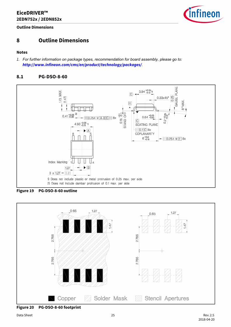
2 Pin Configuration and DescriptionThe pin configuration for all input versions of 2EDN7524F, 2EDN7523F, 2EDN8524F and 2EDN8523F in the PG-DSO-8-60 package is shown in Figure 1. Drawings can be viewed in Chapter 8 (PG-DSO-8-60).
Figure 1 Pin Configuration PG-DSO-8-60, Top View
Table 3 Pin Configuration 2EDN7524F, 2EDN7523F, 2EDN8524F and 2EDN8523F in the PG-DSO-8-60 Package
Pin Symbol Description
1 ENA Enable input channel ALogic input; if ENA is high or left open, OUTA is controlled by INA; ENA low causes OUTA low
2 INA Input signal channel ALogic input, controlling OUTA (inverting or non-inverting)
3 GND Ground
4 INB Input signal channel BLogic input, controlling OUTB (inverting or non-inverting)
5 OUTB Driver output channel BLow-impedance output with source and sink capability
6 VDD Positive supply voltageOperating range 4.5 V/8.6V to 20 V
7 OUTA Driver output channel ALow-impedance output with source and sink capability
8 ENB Enable input channel BLogic Input; if ENB is high or left open, OUTB is controlled by INB; ENB low causes OUTB low
1
2
3
4
8
7
6
5
ENA
INA
GND
INB
ENB
OUTA
VDD
OUTB
Data Sheet 7 Rev. 2.5 2018-04-20
EiceDRIVER™2EDN752x / 2EDN852x
Pin Configuration and Description
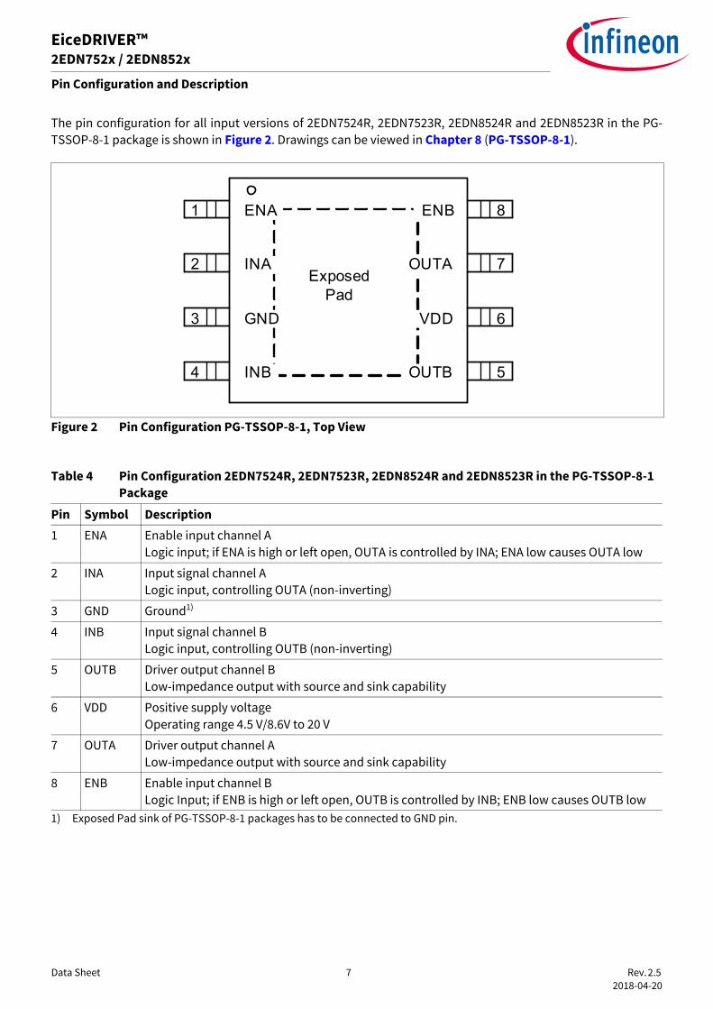
The pin configuration for all input versions of 2EDN7524R, 2EDN7523R, 2EDN8524R and 2EDN8523R in the PG-TSSOP-8-1 package is shown in Figure 2. Drawings can be viewed in Chapter 8 (PG-TSSOP-8-1).
Figure 2 Pin Configuration PG-TSSOP-8-1, Top View
Table 4 Pin Configuration 2EDN7524R, 2EDN7523R, 2EDN8524R and 2EDN8523R in the PG-TSSOP-8-1 Package
Pin Symbol Description
1 ENA Enable input channel ALogic input; if ENA is high or left open, OUTA is controlled by INA; ENA low causes OUTA low
2 INA Input signal channel ALogic input, controlling OUTA (non-inverting)
3 GND Ground1)
1) Exposed Pad sink of PG-TSSOP-8-1 packages has to be connected to GND pin.
4 INB Input signal channel BLogic input, controlling OUTB (non-inverting)
5 OUTB Driver output channel BLow-impedance output with source and sink capability
6 VDD Positive supply voltageOperating range 4.5 V/8.6V to 20 V
7 OUTA Driver output channel ALow-impedance output with source and sink capability
8 ENB Enable input channel BLogic Input; if ENB is high or left open, OUTB is controlled by INB; ENB low causes OUTB low
1
2
3
4
8
7
6
5
ENB
OUTA
VDD
OUTB
GND
ENA
INA
INB
ExposedPad
Data Sheet 8 Rev. 2.5 2018-04-20
EiceDRIVER™2EDN752x / 2EDN852x
Pin Configuration and Description
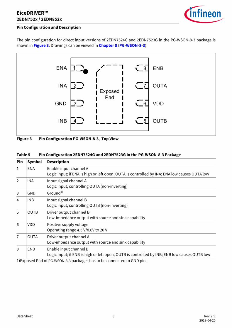
The pin configuration for direct input versions of 2EDN7524G and 2EDN7523G in the PG-WSON-8-3 package isshown in Figure 3. Drawings can be viewed in Chapter 8 (PG-WSON-8-3).
Figure 3 Pin Configuration PG-WSON-8-3, Top View
Table 5 Pin Configuration 2EDN7524G and 2EDN7523G in the PG-WSON-8-3 Package
Pin Symbol Description
1 ENA Enable input channel ALogic input; if ENA is high or left open, OUTA is controlled by INA; ENA low causes OUTA low
2 INA Input signal channel ALogic input, controlling OUTA (non-inverting)
3 GND Ground1)
1)Exposed Pad of PG-WSON-8-3 packages has to be connected to GND pin.
4 INB Input signal channel BLogic input, controlling OUTB (non-inverting)
5 OUTB Driver output channel BLow-impedance output with source and sink capability
6 VDD Positive supply voltageOperating range 4.5 V/8.6V to 20 V
7 OUTA Driver output channel ALow-impedance output with source and sink capability
8 ENB Enable input channel BLogic Input; if ENB is high or left open, OUTB is controlled by INB; ENB low causes OUTB low
8
7
6
5
ENB
OUTA
VDD
OUTB
GND
ENA
INA
INB
2
3
4
1
ExposedPad

Data Sheet 9 Rev. 2.5 2018-04-20
EiceDRIVER™2EDN752x / 2EDN852x
Block Diagram
3 Block DiagramA simplified functional block diagram for the non-inverted / direct version is given in Figure 4. Please refer to thefunctional description section for more details in Chapter 4.
Figure 4 Block Diagram, direct input, pull-up/pull-down resistor configuration
INA
1
2
6
7 OUTA
UVLO
Logic A
ENA
VDD
INB
8
4
5Logic B
ENB
3GND
OUTB
GND
VDD
VDD
VDD
VDD
GND
GND
GND
400k
400k
100k
100k

Data Sheet 10 Rev. 2.5 2018-04-20
EiceDRIVER™2EDN752x / 2EDN852x
Block Diagram
A simplified functional block diagram for the inverted version is given in Figure 5. Please refer to the functionaldescription section for more details in Chapter 4.
Figure 5 Block Diagram, inverting input, pull-up/pull-down resistor configuration
INA
1
2
6
7 OUTA
UVLO
Logic A
ENA
VDD
INB
8
4
5Logic B
ENB
3GND
OUTB
VDD
VDD
VDD
VDD
GND
GND
GND
VDD
VDD
400k
400k
400k 400k

Data Sheet 11 Rev. 2.5 2018-04-20
EiceDRIVER™2EDN752x / 2EDN852x
Functional Description
4 Functional Description
4.1 IntroductionThe 2EDN752x / 2EDN852x is a fast dual-channel driver for low-side switches. Two true rail-to-rail output stageswith very low output impedance and high current capability are chosen to ensure highest flexibility and cover ahigh variety of applications.The focus on robustness at the input and output side additionally gives this device a safety margin in criticalabnormal situations. An extended negative voltage range protects input pins against ground shifts. No currentflows over the ESD structure in the IC during a negative input level. All outputs are robust against reverse current.The interaction with the power MOSFET, even reverse reflected power will be handled by the strong internaloutput stage.All inputs are compatible with LV-TTL signal levels. The threshold voltages with a typical hysteresis of 1.1 V arekept constant over the supply voltage range.Since the 2EDN752x / 2EDN852x aims particularly at fast-switching applications, signal delays and rise/fall timeshave been minimized. Special effort has been made towards minimizing delay differences between the 2channels to very low values of typically 1 ns.
4.2 Supply VoltageThe maximum supply voltage is 20 V. This high voltage can be valuable in order to exploit the full currentcapability of 2EDN752x / 2EDN852x when driving very large MOSFETs. The minimum operating supply voltage isset by the undervoltage lockout function to a typical default value of 4.2 V or of 8 V. This lockout function protectspower MOSFETs from running into linear mode with subsequent high power dissipation.
4.3 Input ConfigurationsAs described in Chapter 1, 2EDN752x / 2EDN852x is available in 2 different configurations with respect to the logicconfiguration of the 4 input pins (input plus enable).The enable inputs are internally pulled up to a logic high voltage, i.e. the driver is enabled with these pins leftopen. The direct PWM inputs are internally pulled down to a logic low voltage. This prevents a switch-on eventduring power up and a not driven input condition. Version with inverted PWM input have an internal pull upresistor to prevent unwanted switch-on.All inputs are compatible with LV-TTL levels and provide a hysteresis of 1.1 V typ. This hysteresis is independentof the supply voltage.All input pins have a negative extended voltage range. This prevents cross current over single wires during GNDshifts between signal source (controller) and driver input.
4.4 Driver Outputs The two rail-to-rail output stages realized with complementary MOS transistors are able to provide a typical 5 Aof sourcing and sinking current. This driver output stage has a shoot through protection and current limitingbehavior. After a switching event, current limitation is raised up to achieve the typical current peak for anexcellent fast reaction time of the following power MOS transistor.The output impedance is very low with a typical value below 0.7 Ω for the sourcing p-channel MOS and 0.5 Ω forthe sinking n-channel MOS transistor. The use of a p-channel sourcing transistor is crucial for achieving true rail-to-rail behaviour and avoiding a source follower’s voltage drop.

Data Sheet 12 Rev. 2.5 2018-04-20
EiceDRIVER™2EDN752x / 2EDN852x
Functional Description
Gate Drive Outputs held active low in case of floating inputs ENx, INx or during startup or power down once UVLOis not exceeded. Under any situation, startup, UVLO or shutdown, outputs are held under defined conditions.
4.5 Undervoltage Lockout (UVLO)The Undervoltage Lockout function ensures that the output can be switched to its high level only if the supplyvoltage exceeds the UVLO threshold voltage. Thus it can be guaranteed, that the switch transistor is not switchedon if the driving voltage is too low to completely switch it on, thereby avoiding excessive power dissipation.The UVLO level is set to a typical value of 4.2 V / 8 V (with hysteresis). UVLO of 4.2 V is normally used for logic levelbased MOSFETs. For higher level, like standard and high voltage superjunction MOSFETS, an UVLO voltage oftypical 8 V is available.
Data Sheet 13 Rev. 2.5 2018-04-20
EiceDRIVER™2EDN752x / 2EDN852x
Characteristics
5 CharacteristicsThe absolute maximum ratings are listed in Table 6. Stresses beyond these values may cause permanent damageto the device. Exposure to absolute maximum rating conditions for extended periods may affect device reliability.
5.1 Absolute Maximum Ratings
5.2 Thermal Characteristics
Table 6 Absolute Maximum Ratings
Parameter Symbol Values Unit Note or Test Condition
Min. Typ. Max.
Positive supply voltage VVDD -0.3 22 V
Voltage at pins INA, INB, ENA, ENB
VIN -10 22 V
Voltage at pins OUTA, OUTB VOUT -0.3 VVDD+0.3 V Note1)
1) Voltage spikes resulting from reverse current peaks are allowed.
-2 VVDD+0.3 V Repetitive pulse <200ns2)
2) Values are verified by characterization on bench.
Reverse current peak at pins OUTA, OUTB
ISNKREV ISRCREV
-5 5
Apk < 500ns
Junction temperature TJ -40 150 °C
Storage temperature TS -55 150 °C
ESD capability VESD 1.5 kV Charged Device Mode (CDM) 3)
3) According to JESD22-C101
ESD capability VESD 2.5 kV Human Body Model (HBM) 4)
4) According to JESD22-A114
Table 7 Thermal Characteristics
Parameter Symbol Values Unit Note or Test Condition
Min. Typ. Max.
Thermal resistance junction-ambient 1)
RthJA25 125 K/W PG-DSO-8-60, Tamb=25°C
Thermal resistance junction-case (top) 2)
RthJC25 66 K/W PG-DSO-8-60, Tamb=25°C
Thermal resistance junction-board 3)
RthJB25 62 K/W PG-DSO-8-60, Tamb=25°C
Characterization parameter junction-top 4)
ΨthJC25 16 K/W PG-DSO-8-60, Tamb=25°C
Characterization parameter junction-board 5)
ΨthJB25 55 K/W PG-DSO-8-60, Tamb=25°C

Data Sheet 14 Rev. 2.5 2018-04-20
EiceDRIVER™2EDN752x / 2EDN852x
Characteristics
5.3 Operating Range
Thermal resistance junction-ambient 1)
RthJA25 64 K/W PG-TSSOP-8-1, Tamb=25°C
Thermal resistance junction-case (top) 2)
RthJP25 56 K/W PG-TSSOP-8-1, Tamb=25°C
Thermal resistance junction-board 3)
RthJB25 55 K/W PG-TSSOP-8-1, Tamb=25°C
Characterization parameter junction-top 4)
ΨthJC25 9 K/W PG-TSSOP-8-1, Tamb=25°C
Characterization parameter junction-board 5)
ΨthJB25 13 K/W PG-TSSOP-8-1, Tamb=25°C
Thermal resistance junction-ambient 1)
RthJA25 61 K/W PG-WSON-8-3, Tamb=25°C
Thermal resistance junction-case (top) 2)
RthJP25 54 K/W PG-WSON-8-3, Tamb=25°C
Thermal resistance junction-board 3)
RthJB25 52 K/W PG-WSON-8-3, Tamb=25°C
Characterization parameter junction-top 4)
ΨthJC25 8 K/W PG-WSON-8-3, Tamb=25°C
Characterization parameter junction-board 5)
ΨthJB25 11 K/W PG-WSON-8-3, Tamb=25°C
1) The junction-to-ambient thermal resistance under natural convection is obtained in a simulation on a JEDEC-standard, high-K board, as specified in JESD51-7, in an environment described in JESD51-2a.
2) The junction-to-case (top) thermal resistance is obtained by simulating a cold plate test on the package top. No specific JEDEC standard test exists, but a close description can be found in the ANSI SEMI standard G30-88.
3) The junction-to-board thermal resistance is obtained by simulating in an environment with a ring cold plate fixture to control the PCB temperature, as described in JESD51-8.
4) The characterization parameter junction-top, estimates the junction temperature of a device in a real system and is extracted from the simulation data for obtaining Rth, using a procedure described in JESD51-2a (sections 6 and 7).
5) The characterization parameter junction-board, estimates the junction temperature of a device in a real system and is extracted from the simulation data for obtaining Rth, using a procedure described in JESD51-2a (sections 6 and 7).
Table 8 Operating Range
Parameter Symbol Values Unit Note or Test Condition
Min. Typ. Max.
Supply voltage VVDD 4.5 20 V Min. defined by UVLO
Logic input voltage VIN -5 20 V
Junction temperature TJ -40 150 °C 1)
1) Continuous operation above 125 °C may reduce life time.
Table 7 Thermal Characteristics (continued)
Parameter Symbol Values Unit Note or Test Condition
Min. Typ. Max.
Data Sheet 15 Rev. 2.5 2018-04-20
EiceDRIVER™2EDN752x / 2EDN852x
Characteristics
5.4 Electrical CharacteristicsUnless otherwise noted, min./max. values of characteristics are the lower and upper limits respectively. They arevalid within the full operating range. The supply voltage is VVDD= 12 V. Typical values are given at TJ=25°C.
Table 9 Power Supply
Parameter Symbol Values Unit Note or Test Condition
Min. Typ. Max.
VDD quiescent current IVDDQU1 0.5 0.7 1.2 mA OUT = high, VVDD= 12 V
VDD quiescent current IVDDQU2 0.3 0.48 0.7 mA OUT = low, VVDD= 12 V
Table 10 Undervoltage Lockout for Logic Level MOSFET
Parameter Symbol Values Unit Note or Test Condition
Min. Typ. Max.
Undervoltage Lockout (UVLO) turn on threshold
UVLOON 3.9 4.2 4.5 V
Undervoltage Lockout (UVLO) turn off threshold
UVLOOFF 3.6 3.9 4.2 V
UVLO threshold hysteresis UVLOHYS 0.3 V
Table 11 Undervoltage Lockout for Standard and Superjunction MOSFET Version
Parameter Symbol Values Unit Note or Test Condition
Min. Typ. Max.
Undervoltage Lockout (UVLO) turn on threshold
UVLOON 7.4 8.0 8.6 V
Undervoltage Lockout (UVLO) turn off threshold
UVLOOFF 6.5 7.0 7.5 V
UVLO threshold hysteresis UVLOHYS — 1.0 — V
Table 12 Logic Inputs INA, INB, ENA, ENB
Parameter Symbol Values Unit Note or Test Condition
Min. Typ. Max.
Input voltage threshold for transition LH
VINH 1.98 2.1 2.2 V
Input voltage threshold for transition HL
VINL 0.95 1.02 1.1 V
Input pull up resistor1)
1) Inputs with initial high logic level
RINH 400 kΩ
Input pull down resistor2)
2) Inputs with initial low logic level
RINL 100 kΩ
Data Sheet 16 Rev. 2.5 2018-04-20
EiceDRIVER™2EDN752x / 2EDN852x
Characteristics
Table 13 Static Output Caracteristics (see Figure 7)
Parameter Symbol Values Unit Note or Test Condition
Min. Typ. Max.
High Level (Sourcing) Output Resistance
RONSRC 0.35 0.7 1.2 Ω ISRC = 50mA
High Level (Sourcing) Output Current
ISRCPEAK 5.0 1)
1) Active limited by design at approx. 6.5Apk, parameter is not subject to production test - verified by design / characterization, max. power dissipation must be observed
A
Low Level (Sinking) Output Resistance
RONSNK 0.28 0.55 1.0 Ω ISNK = 50mA
Low Level (Sinking) Output Current
ISNKPEAK -5.0 2)
2) Active limited by design at approx. -6.5Apk, parameter is not subject to production test - verified by design / characterization, max. power dissipation must be observed
A
Table 14 Dynamic Characteristics (see Figure 6, Figure 7, Figure 8 and Figure 9)
Parameter Symbol Values Unit Note or Test Condition
Min. Typ. Max.
Input/Enable to output propagation delay
TPDlh 15 17 23 ns CLOAD= 1.8 nF, VVDD= 12 V;low to high transition at Input/Enable
Input/Enable to output propagation delay
TPDhl 15 19 23 ns CLOAD= 1.8 nF, VVDD= 12 Vhigh to low transition at Input/Enable
Input/Enable to output propagation delay mismatch between the two channels on the same IC
delta tPD 2 ns
Rise Time TRISE — 5.3 10 1)
1) Parameter verified by design, not 100% tested in production.
ns CLOAD= 1.8 nF, VVDD= 12 V
Fall Time TFAll — 4.5 10 1) ns CLOAD= 1.8 nF, VVDD= 12 V
Minimum input pulse width that changes output state
TPW — 6 10 1) ns CLOAD= 1.8 nF, VVDD= 12 V
Data Sheet 17 Rev. 2.5 2018-04-20
EiceDRIVER™2EDN752x / 2EDN852x
Timing Diagrams
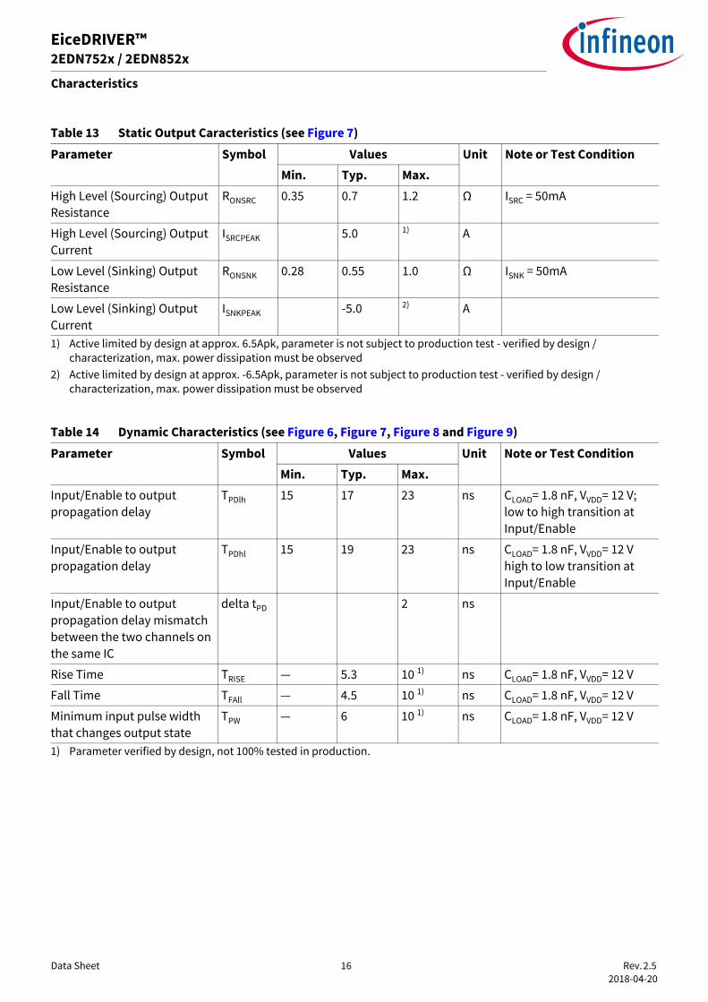
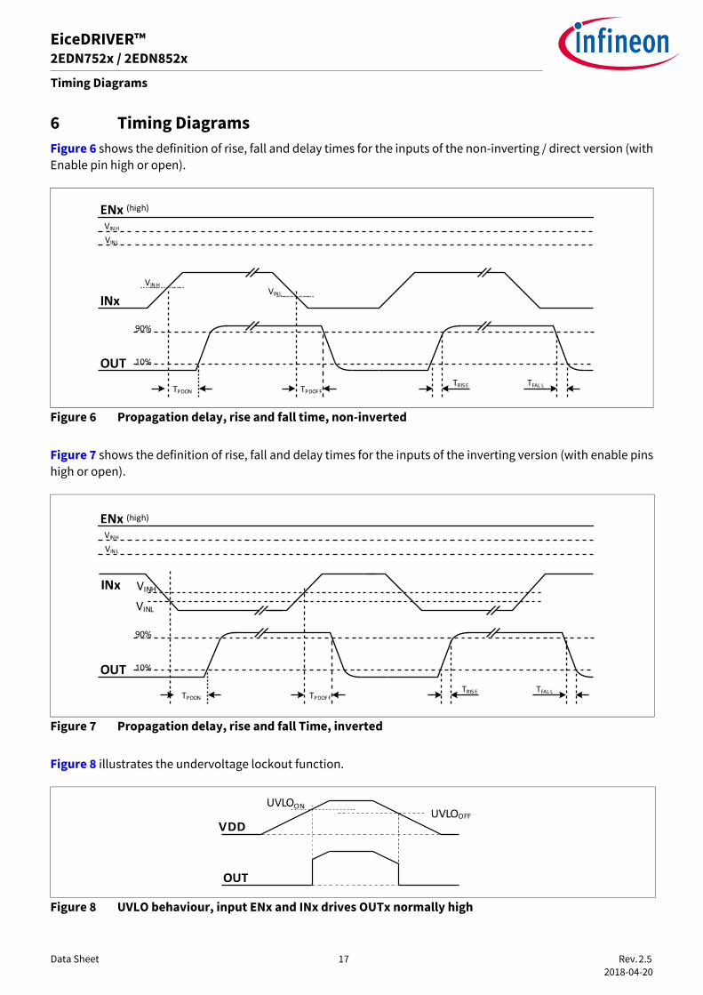
6 Timing DiagramsFigure 6 shows the definition of rise, fall and delay times for the inputs of the non-inverting / direct version (withEnable pin high or open).
Figure 6 Propagation delay, rise and fall time, non-inverted
Figure 7 shows the definition of rise, fall and delay times for the inputs of the inverting version (with enable pinshigh or open).
Figure 7 Propagation delay, rise and fall Time, inverted
Figure 8 illustrates the undervoltage lockout function.
Figure 8 UVLO behaviour, input ENx and INx drives OUTx normally high
INx
OUT
TPDON
VIN H
90%
TPDOF F
TRIS E TFAL L
10%
VINL
ENxVIN H
VINL
(high)
INx VINH
VINL
OUT
TPDON TPDOF F
TRIS E TFAL L
ENxVINH
VIN L
90%
10%
(high)
OUT
VDD
UVLOONUVLOOFF

Data Sheet 18 Rev. 2.5 2018-04-20
EiceDRIVER™2EDN752x / 2EDN852x
Timing Diagrams
Figure 9 illustrates the minimum input pulse width that changes output state.
Figure 9 TPW, minimum input pulse width that changes output state
INx
OUTx
VIN H
90%
VINL
ENxVIN H
VINL
(high)
TPW

Data Sheet 19 Rev. 2.5 2018-04-20
EiceDRIVER™2EDN752x / 2EDN852x
Typical Characteristics
7 Typical Characteristics
Figure 10 Undervoltage lockout 2ED7x (4.2V)
Figure 11 Undervoltage lockout 2ED8x (8V)
3.7
3.9
4.1
4.3
4.5
-50 0 50 100 150
VD
D [V
]
T junction [°C]
UVLO ON/OFFvs
TEMPERATURE
on value
off value
Inx, ENx highIndication Outx
0.2
0.25
0.3
0.35
0.4
-50 0 50 100 150V
DD
de
lta [
V]
T junction [°C]
UVLO HYSTERESISvs
TEMPERATURE
Inx, ENx high
Indication Outx
6.4
6.8
7.2
7.6
8
8.4
8.8
-50 0 50 100 150
VD
D [V
]
T junction [°C]
UVLO ON/OFFvs
TEMPERATURE
on value
off value
Inx, ENx highIndication Outx
0.85
0.9
0.95
1
1.05
-50 0 50 100 150
VD
D d
elta
[V
]
T junction [°C]
UVLO HYSTERESISvs
TEMPERATURE
Inx, ENx high
Indication Outx
Data Sheet 20 Rev. 2.5 2018-04-20
EiceDRIVER™2EDN752x / 2EDN852x
Typical Characteristics
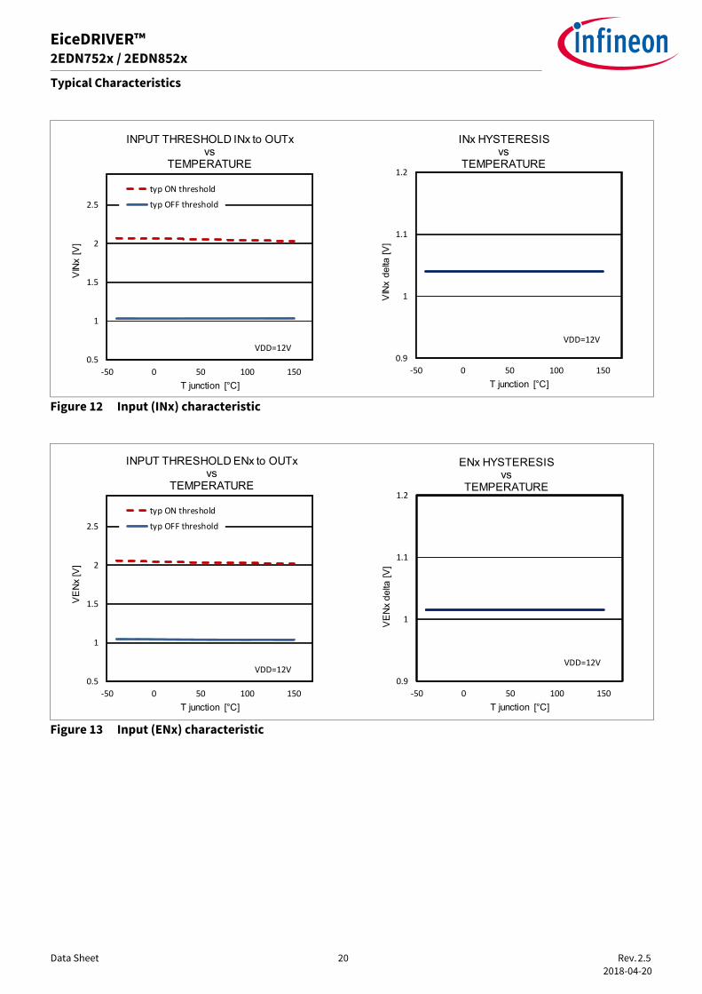
Figure 12 Input (INx) characteristic
Figure 13 Input (ENx) characteristic
0.9
1
1.1
1.2
-50 0 50 100 150
VIN
x d
elta
[V
]T junction [°C]
INx HYSTERESISvs
TEMPERATURE
VDD=12V
0.5
1
1.5
2
2.5
-50 0 50 100 150
VIN
x [V
]
T junction [°C]
INPUT THRESHOLD INx to OUTxvs
TEMPERATURE
typ ON threshold
typ OFF threshold
VDD=12V
0.5
1
1.5
2
2.5
-50 0 50 100 150
VE
Nx
[V]
T junction [°C]
INPUT THRESHOLD ENx to OUTxvs
TEMPERATURE
typ ON threshold
typ OFF threshold
VDD=12V0.9
1
1.1
1.2
-50 0 50 100 150
VE
Nx
de
lta [
V]
T junction [°C]
ENx HYSTERESISvs
TEMPERATURE
VDD=12V

Data Sheet 21 Rev. 2.5 2018-04-20
EiceDRIVER™2EDN752x / 2EDN852x
Typical Characteristics
Figure 14 Propagation delay (INx) on different input logic levels (see Figure 6)
Figure 15 Propagation delay (ENx) on different input logic levels (see Figure 6)
12.5
15
17.5
20
22.5
25
-50 0 50 100 150
TP
D [n
s]
T junction [°C]
VINx to OUTx PROPAGATION DELAYvs
TEMPERATURE
typ input rise-up
typ input fall-down
VDD=12V
Input 5V
15
17.5
20
22.5
25
-50 0 50 100 150
TP
D [n
s]T junction [°C]
VINx to OUTx PROPAGATION DELAYvs
TEMPERATURE
typ input rise-up
typ input fall-down
VDD=12VInput 3.3V
15
17.5
20
22.5
25
-50 0 50 100 150
TP
D [n
s]
T junction [°C]
VENx to OUTx PROPAGATION DELAYvs
TEMPERATURE
typ input rise-up
typ input fall-down
VDD=12VEnable 5V VDD=12VEnable 5V
15
17.5
20
22.5
25
-50 0 50 100 150
TP
D [n
s]
T junction [°C]
VINx to OUTx PROPAGATION DELAYvs
TEMPERATURE
typ input rise-up
typ input fall-down
VDD=12VInput 3.3V
Data Sheet 22 Rev. 2.5 2018-04-20
EiceDRIVER™2EDN752x / 2EDN852x
Typical Characteristics
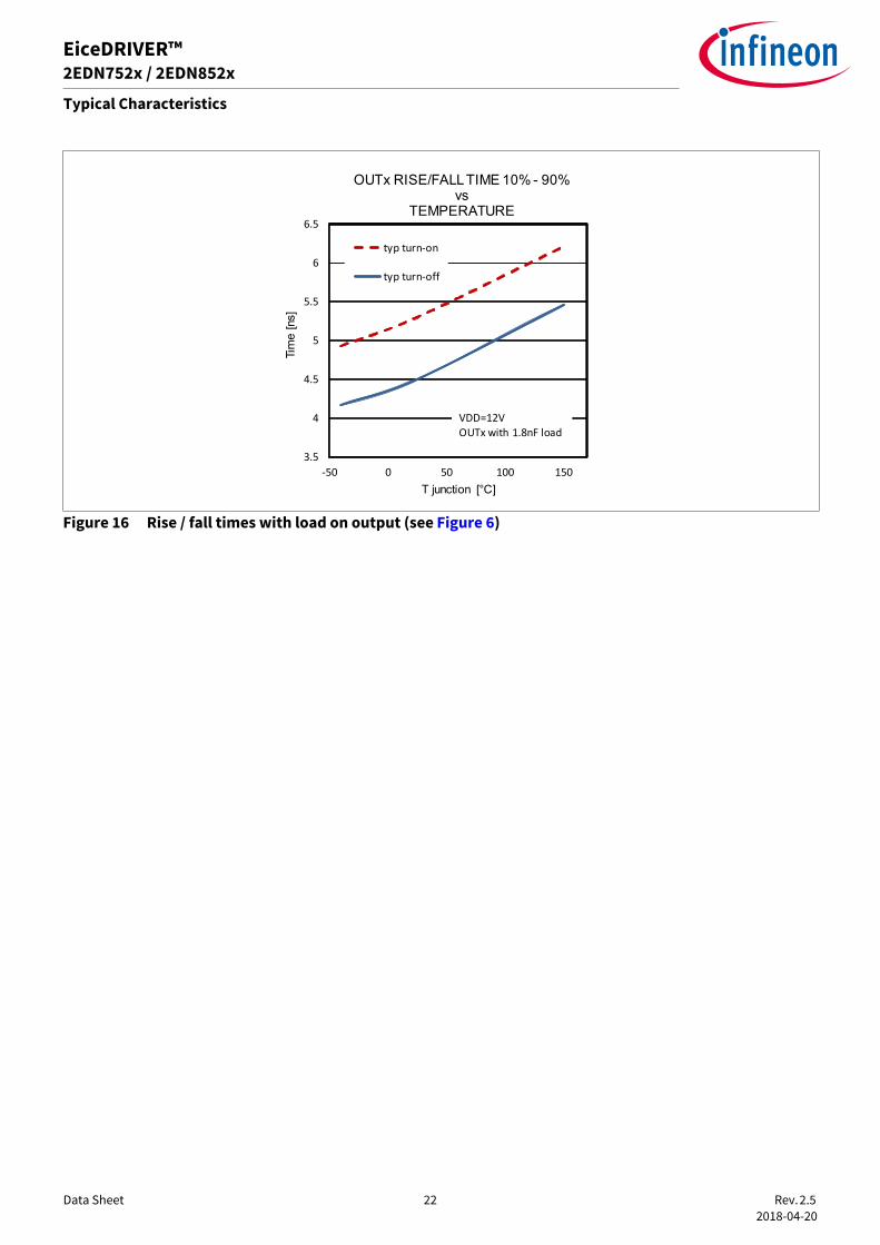
Figure 16 Rise / fall times with load on output (see Figure 6)
3.5
4
4.5
5
5.5
6
6.5
-50 0 50 100 150
Tim
e [n
s]
T junction [°C]
OUTx RISE/FALL TIME 10% - 90%vs
TEMPERATURE
typ turn-on
typ turn-off
VDD=12VOUTx with 1.8nF load

Data Sheet 23 Rev. 2.5 2018-04-20
EiceDRIVER™2EDN752x / 2EDN852x
Typical Characteristics
Figure 17 Power consumption related to temperature, supply voltage and frequency
0.2
0.4
0.6
0.8
0 10 20
IDD
[m
A]
VDD [V]
CURRENT CONSUMPTIONvs
OPERATING SUPPLY VDD
OUTx High
OUTx Low
Tj=25°CENx floating (VDD)
0.30
0.40
0.50
0.60
0.70
0.80
-50 0 50 100 150
IDD
[m
A]
T junction [°C]
CURRENT CONSUMPTIONvs
TEMPERATURE
OUTx High
OUTx Low
VDD=12VENx NC
0
10
20
30
40
50
0 250 500 750 1000
I D
D [
mA
]
Frequency [kHz]
CURRENT CONSUMPTIONvs
FREQUENCY
VDD 4,5V
VDD 12V
VDD 20V
Tamb 25°C
Input 50%@3.3VDevice self-heatingLoad 1.8nF serial
Data Sheet 24 Rev. 2.5 2018-04-20
EiceDRIVER™2EDN752x / 2EDN852x
Typical Characteristics
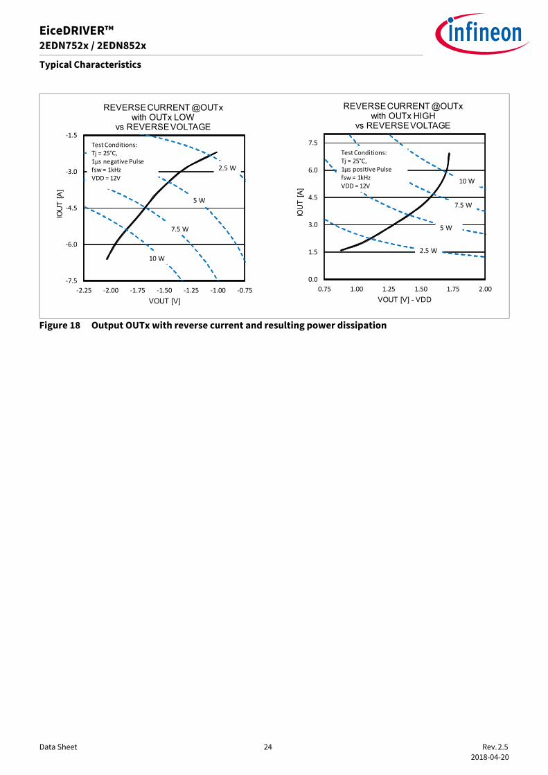
Figure 18 Output OUTx with reverse current and resulting power dissipation
-7.5
-6.0
-4.5
-3.0
-1.5
-2.25 -2.00 -1.75 -1.50 -1.25 -1.00 -0.75
IOU
T [
A]
VOUT [V]
REVERSE CURRENT @OUTx with OUTx LOW
vs REVERSE VOLTAGE
10 W
7.5 W
5 W
2.5 W
Test Conditions:Tj = 25°C,1µs negative Pulsefsw = 1kHzVDD = 12V
0.0
1.5
3.0
4.5
6.0
7.5
0.75 1.00 1.25 1.50 1.75 2.00
IOU
T [
A]
VOUT [V] - VDD
REVERSE CURRENT @OUTx with OUTx HIGH
vs REVERSE VOLTAGE
10 W
7.5 W
5 W
2.5 W
Test Conditions:Tj = 25°C,1µs positive Pulsefsw = 1kHzVDD = 12V
Data Sheet 25 Rev. 2.5 2018-04-20
EiceDRIVER™2EDN752x / 2EDN852x
Outline Dimensions
8 Outline Dimensions
Notes
1. For further information on package types, recommendation for board assembly, please go to:
http://www.infineon.com/cms/en/product/technology/packages/.
8.1 PG-DSO-8-60
Figure 19 PG-DSO-8-60 outline
Figure 20 PG-DSO-8-60 footprint

Data Sheet 26 Rev. 2.5 2018-04-20
EiceDRIVER™2EDN752x / 2EDN852x
Outline Dimensions
Figure 21 PG-DSO-8-60 packaging
8.2 PG-TSSOP-8-1
Figure 22 PG-TSSOP-8-1 outline

Data Sheet 27 Rev. 2.5 2018-04-20
EiceDRIVER™2EDN752x / 2EDN852x
Outline Dimensions
Figure 23 PG-TSSOP-8-1 footprint
Figure 24 PG-TSSOP-8-1 packaging

Data Sheet 28 Rev. 2.5 2018-04-20
EiceDRIVER™2EDN752x / 2EDN852x
Outline Dimensions
8.3 PG-WSON-8-3
Figure 25 PG-WSON-8-3 outline
Figure 26 PG-WSON-8-3 footprint
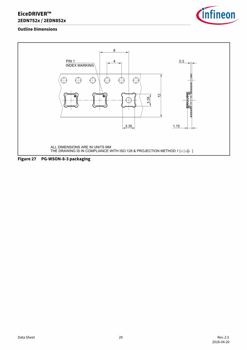
Data Sheet 29 Rev. 2.5 2018-04-20
EiceDRIVER™2EDN752x / 2EDN852x
Outline Dimensions
Figure 27 PG-WSON-8-3 packaging
Data Sheet 30 Rev. 2.5 2018-04-20
EiceDRIVER™2EDN752x / 2EDN852x
Revision History
9 Revision History
Page/ Item Subjects (major changes since previous revision) Responsible
Rev. 2.5, 2018-04-20
29 Update package diagram for PG-WSON Vincent Zhang
Rev. 2.4, 2017-08-18
updated from version 2.3
24correct typo (VOUT [V] - VDD), add detail for test condition (VDD = 12V) Figure 18
Tobias Gerber
13add min. voltage reference for OUTA, OUTB in reverse current condition. (Note 1) Table 6
Tobias Gerber
TrademarksAll referenced product or service names and trademarks are the property of their respective owners.
Edition 2018-04-20Published by Infineon Technologies AG81726 Munich, Germany
© 2018 Infineon Technologies AG.All Rights Reserved.
Do you have a question about any aspect of this document?Email: [email protected]
Document reference
IMPORTANT NOTICEThe information given in this document shall in noevent be regarded as a guarantee of conditions orcharacteristics ("Beschaffenheitsgarantie"). With respect to any examples, hints or any typicalvalues stated herein and/or any information regardingthe application of the product, Infineon Technologieshereby disclaims any and all warranties and liabilitiesof any kind, including without limitation warranties ofnon-infringement of intellectual property rights of anythird party. In addition, any information given in this document issubject to customer's compliance with its obligationsstated in this document and any applicable legalrequirements, norms and standards concerningcustomer's products and any use of the product ofInfineon Technologies in customer's applications. The data contained in this document is exclusivelyintended for technically trained staff. It is theresponsibility of customer's technical departments toevaluate the suitability of the product for the intendedapplication and the completeness of the productinformation given in this document with respect tosuch application.
For further information on technology, delivery termsand conditions and prices, please contact the nearestInfineon Technologies Office (www.infineon.com).
WARNINGS
Due to technical requirements products may containdangerous substances. For information on the typesin question please contact your nearest InfineonTechnologies office.
Except as otherwise explicitly approved by InfineonTechnologies in a written document signed byauthorized representatives of Infineon Technologies,Infineon Technologies’ products may not be used inany applications where a failure of the product or anyconsequences of the use thereof can reasonably beexpected to result in personal injury.