Embed Size (px)
Citation preview
7RD-R147 7:15 ENC ENHANCED CONSTANT
'Z MODULTOR(U) ITT /
AER'OSPACE/OPTICAL DIV FORT WAYNE IND R E REED JUNI 84
UNCL7FIED FG9/5 NL
EhhhE~mEENDE

ILI U-0
wk.
MICROCOPY RESOLUTION TEST CHARTNATIONA BUREA OF STMIDAOS-1963-A
-- t ." -° -% % " -% % " ." % % b % - - -"- ' , , - , . . . , - 4i - o - o t ,
- .*...-. -.....-*.
44
RADC-Th-84-117Filnl Technicl ReportJune 1964
L%)
:. EMC ENHANCED CONSTANT "Z"" MODULATOR
IT
.LRoed
, B
ROME AIR DEVELOPMENT CENTERAir Force Systems Commandif Grifflas Air Force Base. NY 13441
07
e .
a, *-4i ..*. 4
This report has been reviewed by the RADC Public Affairs Office (PA) andis releasable to the National Technical Information Service (NTIS). At NTISit will be releasable to the general public, including foreign nations.
RADC-TR-84-117 has been reviewed and is approved for publication.
APPROVED: "~-L
THOMAS E. BAUSTERTProject Engineer
APPROVED:
W. S. TUTHILL, Colonel, USAFChief, Relilability & Compatibility Division
FOR THE COMMANDER:
JOHN A. RITZActing Chief, Plans Office
0
* - If your address has changed or if you wish to be removed from the RADC mailinglist, or if the addressee is no longer employed by your organization, pleasenotify RADC (RBCT) Griffiss APB NY 13441. This will assist us in maintaininga current mailing list.
Do not return copies of this report unless contractual obligations or noticeson a specific document requires that it be returned.
•-notiy RDC (BCT Crifis AFBNY 3441 Ths wil asistus n manta11A

SECURITY CLASSIFICATION OP THIS PAGE
REPORT DOCUMENTATION PAGEI& REPORT SECURITY CLASSIFICATION %b. RESTRICTIVE MARKINGSUNCLASSIFIED N/A
*2,L SECURITY CLASSIFICATION AUTHORITY 3. OISTRIBUTION/AVAILASILITY OP REPORT
N/A Approved for public release;aC OCLASSIPICATION/DOWNGRAOING SCHEDULE1 distribution unlimited
N/A 1_____________________
4, PER4FORMING ORGANIZATION ARPORT NUMBR(S) S. MONITORING ORGANIZATION REPORT NUMBER($)
R&DC-TR-84-117N/A
"a NAME OP PERFORMING ORGANIZATION OPP OFICE SYMBOL Ua NAME Of MONITORING ORGANIZATIONITTIAerospace/Optical Division Rome Air Development Center (RBCT)
6c. ACORIESS (City. State end ZIP Code) Tb. ACCIRESS V(ity. Siteand ZIP Code)
P. 0. Box 3700 Griffiss AFB NY 13441Ft Wayne IN 46801
G& NAME OP PUNOING/SFONSORING OPP OFICE SYMBOL 9. PROCUREMENT INSTRUMENT IDENTIFICATION NUMBERORGANIZATION (ifaplibe)
Rome Air Development Center RBCT F30602-83-C...oolft. ADDRESS (City. Stalt and ZIP Code) 10. SOURCE OP FUNDING NO.
PROGRAM PROET TAK WR UNITGriffiss AFn NY 13441 ELEMENT No. NO.c NO.BNO
62702F 2338 043111. TITLE (include Securhty Claujjicatiout
j EMC ENHANCED CONSTANT "Z" MODULATOR12. PERSONAL AUTHOR(S)
R. E. Reed13a. TYPE OP RPORT 131. ime COVERED o No 8 14. ATE OP RPORT (Y.. M .. DYj S PAG O N
Fina 1PROM Feb83 roNv3June 1984 _7 6816. SUPPLEMENTARY NOTATION
N/A
1T. COSATI CODES Is. SJECT TERMS (Continue on uwuerme it'necemsty and identify by block numberi
FIELD GROUP $USO. ModulationUJ Incidental FM
IPIN Diode13. ABSTRACT (Continue on ,Weene if ne..ma, and identify by block number)The EMC Enhanced constant *ZP modulator (EECZM) research and development effort at ITT-A/OD was undertaken to provide an amplitude modulation capability for a low-noise, mediumpower (1 Watt), wideband (225-400 MHz), frequency hopping (1000 hops/sec) synthesizercurrently in development at the ITT-A/OD facility for RADC. The primary objective was toamplitude modulate the synthesizer's RF carrier to the required modulation percentage whileavoiding frequency modulation of the RF carrier
7AN1 RE carrier amplitude modulator can seriously degrade synthesizer noise performancePthrough modulator impedance changes during the modulation cycle. This change in impedancecauses frequency modulation of the synthesizer's voltage controller oscillator (VCO) re-sulting in RF carrier FM sidebands extending far beyond the AM sidebands for a large modula-
* tion index. Usually the modulator is isolated from the VCO by 20 to 30 dB of buffer ampli-fication to minimize VCO frequency modulation; however, buffer amplifiers tend to degrade
20. DIST RIE@UTION/AVAI LABILITY OF ASTRACT 21. ABSTRACT SECURITY CLASSIFICATION
UNCLASSIFIEO/UNLIMITEO C1SAME AS RFT. 0 OTIC USERS 03 UNCLASSIFIED22& NAME OP RESPONSIBLE INDIVIDUAL l22b. TELEPHONE NUMBER 22. OPPICE SYMBOL
Thomas E. Baustert .(315) 330-3490 RADC/RBCT
DO FORM 1473, 83 APR EDITION OP I JAN 731IS OBSOLETE. VKC..J IASIFIEDSECURITY CLASSIFICATION OP THIS PAR I
MEZVq , N

UNCLASSIFIED
SICURLTY CL.ASUIPCATIO OP I4S PASS
Item #19 Continued
the overall synthesizer noise performance. By controlling the modulator's impedance to theVCO during the modulation cycle, the VCO buffer stages can be omitted while RF carrierfrequency modulation is minimized. ....
The program approach centered about reviewing a previous IR&D effort at ITT-A/OD relatingto a constant impedance amplitude modulation scheme and culminated in a breadboard, andultimately a feasibility model, to meet the modulator's statement-of-work (SOW) requirements
A major portion of the R&D effort focused on design and test of the modulator's constantimpedance attenuator. Several modulator designs were modeled resulting in adoption ofa hybrid coupler/PIN diode attenuation scheme. This type of modulator impresses audio modu-lation onto the synthesizer's RF carrier via PIN diodes terminating a hybrid coupler whileproviding a constant impedance to the VCO during the modulation cycle.
DTIC1 F-CTE
,1NOV 20 M
AcCesslon For
NTIS GRA&IDTIC TAB 13Unannounced QiJu.;t i ricati on
-Distribution/
Availability CodesAvail and/or
D i stI Special
UNCLASSIFIEDWSCUAITY CLASPICA"ION OP ThIS PAGE
- Emi

Table of Contents
Paragraph Title pageSection 1
1.2 Program Description. 666.66666 ..................... 11.3 Report Organization..... 000*000000660000000000000000 11.4 Modulator Specifications..so..000...0...000....0.. 1
Section 2
AMPLITUDE MODULATOR SYSTEM REQUIREMENTS - THE EMC PROBLEM 3
Section 3
TECHNICAL APPROACH
3. 1 SYSTEM ANALYSI......... ............... oo...... 53.1.1 Modulation Ana............. 666666666666000*000 736.1.2 Incidental FM Analysis... ....................... .. 83.1.3 Noise Analysiso. ........... 000600*600000*009000060 83.2 Modulator Design ... .. 00.00........................ 123.2.1 Buffer ..... i.... ........00000 00006.6......00 123.2o2 Electronically Controlled Pin Diode Attenuator..... 163.2.2.1 Controlled PIN Diode Attenuator.................... 163.2.2.2 Hybrid Coupled-Isolated PIN Diode Attenuatoreoeeeoe 193o2.3 Forward Power Detector.. 6 .. *000................. 213.2.4 Interface and Control Circuits*.................... 283.2.4.1 Interface .... l........ .......................... 283.2.4.2 Band Shaping Network............................... 303.2.4.3 Modulation/ALC Control...... 66666666666666666666666 303.2.5 Mechanical Requirementos.. 666666666666666666666666 333.2o6 System T............. 6666666ooo606666666666***s6 35
Section 4
SYSTEM TESTS
4.1 Modulator Test Results............................. 3746161 Frequency R..... ................ 6666666666666 374.1o2 Input ................. 666 666666 66 66 66 66666666 34.1.3 Input/Output Impedance... 66e66*6666666*o**666*66*66 374.1.4 Insertion Loss ....... ............. 374.1.5 Output Signal-to-Noise (S/N) Degradation...........: 394.1.6 Incidental FM (IFM) ... o0........................... 394.1o7 Modulation Bandwidth.. 6* 6*6*60600066666666666 394.1.8 Modulation Capability...... ........................ 394.1.9 Distortiono..6 66666 ............. 66 66 666666666 66 6 404.1.10 Modulation Input Iupedance......................... 404.2 Test Data Summry. 6*6*o6666*666666666666oo*666*6*6 40
11I IN
Table of Contents (Continued)
Paragraph Title page
Section 5
CONCLUSIONS AND RECOMMENDATIONS
5.1 Conclusions...s ............ooooe.........e.s... 41
5.2 Recoemndations...........e ..oo e.......**e.~ee 41
Section 6
APPENDIX A-1
am =''

List of Figures
Figure Title Page
3.1-1 Block Diagram of a Transmitter with theConstant Z Moduat.*.. .............. 6
3.1.3-1 Noise Model for the Modulator...................... 93.1.3-2 Buffer Amplifier Noise Figure Versus Output
3.2-1 Modulator Detailed Schematic ............ 133.2.1-1 Buffer Amplifier Frequency Response................oo 153.2.2.1-1 Controlled PIN Diode Attenuator.................... 173.22.2-1 1-Stage 'of a 3-Stage Hybrid Coupled-Isolated
PIN Diode Attenuator.. ...... ...... ....... .... 203.2.2o2-2 Hybrid Coupler, PIN Diode Attenuator
Characteristics .............. ... 223.2.2.2-3 Attenuator Characteristic...5...5 ... ......... ..... 233.2.2o2-4 3-Stage Hybrid Coupled Attenuator Construction.. ... 243.2o3-1 Voltage Sauple..................................... 253.*2.*3-2 Current Sa....... ..................... s........... 253.2.3-3 Forward Power Detector............................. 273.2.4.1-1 Interface Netvork.............................. .. ss 293.2.4.2-1 Band Shading Network......55 se... oooo so...... 313.2.4.3-1 Control Amplifier/Attenuator Driveroeo..............9 323.2.5-1 Modulator Enclosure., se.... es...se.... 343o2.5-2 Modulator Package Coucept.......................... 36
List of Table.
Table Title Page
1.4-1 Constant "Z" Modulator Goals and Specifications.... 2
3.1.3-1 N/S Degradation/dB ........ ......... oos.s .... ...... 123.2.1-1 N/S Degradation/dB. ............ 00s...... see...... .. 143.2.2-1 Attenuator Characteristicse........................ 163.2.2.1-1 PIN Diode Attenuator Characteristics**@............ 193.2.4.1-1 Modulation Requiremnts.................... ........ 28
4.1-1 System Final Test.Results.......................... 38
- ~Iii
1% glum

ABSTRACT
This final report covers the design concept and feasibility
model for a UHF-medium power (2 watts) EMC Enhanced Constant "Z"Modulator (EECZM). The program augments an on-going developmentaleffort at ITT-A/OD of a low-noise medium power'wideband (225-400 MEhz)frequency hopping (1000 hops/see) synthesizer. The deliverable feasi-bility model meets, or exceeds, all critical design parameters whentested as a stand-alone equipment or while modulating the low-noisesynthesizer's RF carrier.
C0
-iv
Final ReportFor
EMC Enhanced Constant "Z" Modulator
Section 1
1.1 Introduction
This final report describes the theory, design, and eva-
luation of an EKC Enhanced Constant "Z" Modulator (EECZH) feasibilitymodel designed to operate in conjunction with a low-noise, UHF fre-quency hopping synthesizer. The EECZM impresses amplitude modulationonto an RF carrier (225-400 MHz) via hybrid coupler-PIN diode atte-nuator. The EECZM presents a constant source impedance to preventincidental frequency modulation. Automatic level control (ALC) guaran-tees that the modulation percentage is independent of the carrieramplitude.
1.2 Program Description
The program was initiated with the design, construction,
and test of critical modulator circuitry. Optimization of the modula-
tor breadboard led to a redesign of the modulator from a controlled PINdiode arrangement to a hybrid coupled isolated PIN diode configuration.Successful modulator breadboard test results were the basis for the
construction and test of the modulator feasibility model. The modelwas evaluated for such critical parameters as insertion loss, source
frequency pulling, source signal-to-noise degradation and modulation
percentage as .a function of input frequency. The feasibility modeltests proved the success of the program.
1.3 Report Organization
The EECZH final report is organized as shown:
Section 2 EECZM Requirements - The EMC ProblemSection 3 Program Technical ApproachSection 4 Program Final TestSection 5 Conclusions and RecommendationsSection 6 Appendix
1.4 Modulator Specifications
Table 1.4-1 lists the modulator's goals and specifications
as delineated in the program's statement of work (SOW).

Nd C%1
VVI 0
8 Ia
-44
0
4,4
4 W4 0 N0 0 -4 -
-40 n $ 0 Nt AH 00 4
0 W 0 0 0+1N+1 1+0441zng z R 0 amMaeCIn I IAC 0 c 0C4 0a - 0 0 %c N4 00 in0 mm 00
4 41
0
* -p4
110 0 '4 w 00 C4
0L 41 V4 -
0 m bo
.1. 1 .4J1.41 00-
a~~ ~ ~ coa r44.8
0.00 : Do 40 cc 0
w2 I

Section 2
AMPLITUDE MODULATOR SYSTEM EQUIREMENTS - THE EMC PROBLEM
Receiver degradation caused by off-channel transmitters isa problem that has been recognized since the early days of radio. Theuse of solid-state technology in modern communications equipment has,in many cases, made the problem more severe. The low-noise, crystaloscillator has been replaced by the noisy digital synthesizer. Thenarrowband, vacuum-tube power amplifier has been replaced by a solid-state power amplifier with bandwidths and noise that covers many octa-ves. The vacuum-tube receiver has given way to the solid-statereceiver that, in many cases, has inferior signal handling capabili-ties. High-Q, mechanically-tuned preselectors are being replaced byvaractor-tuned filters, which not only have less selectivity, but alsogenerate additional distortion. At the same time, the number of radiosystem has increased and user requirements often dictate collocatedoperation. The receiver degradation caused by noise and off-channelsignals is often referred to as desensitization, one of the majorelectromagnetic compatibility (EMC) problem.
Transmitter noise poses a particularly difficult problem
because output noise is broadband. Unlike a transmitter spurious out-put broadband noise can degrade performance over a wide frequency rangerather than a single channel. The output noise of a transmitter canonly be minimized by generating the carrier with a high power oscilla-tor in the synthesizer so that the required gain of the stagesfollowing the oscillator is minimized. Low level, low-noise oscilla-tors followed by several stages of gain to produce the requiredtransmitter output power is not a viable approach because the noisecontributed by the gain stages degrades the noise performance of thetransmitter.
The phase noise associated with a VCO occurs at frequenciesnear the carrier and hence can not easily be reduced by filtering.
Care must be taken in the overall design of a transmitter so that phasenoise is held to a minimum.
An amplitude modulator can seriously degrade synthesizernoise performance because the impedance of the modulator changes duringthe modulation cycle. This change in impedance causes frequency modu-lation of the Voltage Controlled Oscillator (VCO) in the synthesizer.The PM sidebands can extend beyond the AM sidebands if the modulationindex is large.
3

Experience with this problem at ITT-A/OD has shown thateven 20 or 30 dB of isolation between the modulator and the VCO may notbe sufficient to reduce the frequency modulation to acceptable levelsand that isolation, along with a reduction of the impedance changes inthe modulator, is required to reduce the frequency modulation of theVCO to an acceptable level. Therefore, isolation provided by a bufferamplifier and an isolator will Lot reduce the frequency modulation ofthe VCO sufficiently to meet the specifications of the EECZM. Up.
The technique of using high-level oscillators and minimumgain following the oscillator to minimize transmitter output noisemakes it more difficult to control frequency modulation of the oscilla-tor because there is less isolation between the oscillator and themodulation than in a transmitter using a low-level oscillator.
04
.?
':
- K
"4
* 4
%... %% %%,%

Section 3
TECHNICAL APPROACH
There are several ways to amplitude modulate a transmitter.The modulation process can be incorporated into a feedback system or itcan be accomplished without feedback. An example of the latter tech-nique is to apply the modulating signal to the collectors of the finalamplifier and its driver stage. This technique requires a high-powermodulator, but the RF amplifiers do not have to be linear. This typeof modulation can also be used with the low-power amplifier in thetransmitter, but then all stages following the last modulated stagemust be linear to preserve the modulation envelope. Modulation canalso be applied to the bases of the transistors in the RF amplifierchain, but again all stages following the modulated stages must belinear. In either case, the input impedance of the transistors willchange during the modulation cycle and cause incidental FM because thesynthesizer is not presented with a constant load impedance.
Another technique uses a 90* hybrid with one of the outputports connected to a device like a PIN diode, which has its impedancechange with the modulating signal. The other output port is connectedto the antenna terminal or power amplifier. One of the input ports isconnected to a matched load while the other is -onnected to the driverstage. Two cascaded hybrid modulators are required to achieve a highpercentage modulation because the isolation of the hybrid over the 225to 400 MHz band is only about 20 dB. Although this technique offers areduction in impedance change with modulation, it will not meet therequirements of the EMC Enhanced Constant "Z" Modulator.
Any of these techniques can be used with a feedback loop toreduce distortion. With a feedback loop, the stages following themodulated stage do not have to be linear. However, they will not meetthe EECZM requirements because the change in input impedance is toolarge.
3.1 SYSTEM ANALYSIS
The ITT-A/OD approach utilizes an electronicallycontrolled constant impedance attenuator in the transmitter signalpath. See Figure 3.1-1.
To minimize the noise performance degradation caused by theattenuator, a buffer amplifier preceeds the attenuator. The gain ofthe buffer amplifier is equal to the loss in the attenuator so thatwith a 30 dBm input from the synthesizer, the output of the attenuatoris 30 dBm. If the buffer amplifier followed the attenuator, the noise-to-signal ratio at the output of the modulator would be greater thanthat allowed by the total system.
I

acK
I.-
"4
Ibe
C)a
t
cnCCa
CDS
P4"
z 0. La&nd
)I-a

The input impedance of the PIN diode attenuator must remainconstant over the modulation cycle to ensure that the synthesizer isrelatively free of incidental FM.
Automatic level control (ALC) is also incorporated into thedesign of the modulator. The power detector samples the output signaland the detected sample is used for linearizing the modulator and ALC.Provision is also made for adding a power amplifier inside the feed-back loop. The modulator has been integrated into the design of atransmitter rather than just being an add-on to the synthesizer.
PIN diodes are used as the controlled circuit elements inthe Constant Z variable attenuator. The only critical considerationwhen choosing the PIN diodes is the carrier lifetime. The carrierlifetime must be long when compared with the time for an RF cycle, butshort when compared with the time for one cycle at baseband. The PINdiode must have a carrier lifetime on the order of 0.6 US. Thesediodes are readily available.
3.1.1 Modulation Analysis
The baseline modulator is an electronically controlledattenuator that modulates the carrier by controlling the carrier ampli-tude. The carrier must be attenuated with no modulation applied sothat upward modulation is produced by reducing the attenuation. Forexample, for 100-percent upward modulation, the unmodulated carriermust be attenuated 6 dB because the peak envelope power of a100-percent amplitude modulated signal is 6 dB larger than the unmodu-lated carrier. The attenuation required for any modulation index, m,for upward modulation is:
ou - 20 LOG (m + 1) (1)
This is the amount that the unmodulated carrier must be attenuated.
The attenuation required for any modulation index (m), fordownward modulation is:
a)- - 20 LOG (1-) (2)
For 100-percent downward modulation, infinite attenuationis required to reduce the modulation envelope to zero; therefore,
100-percent downwards modulation is not possible with this type ofmodulator.
To meet the 85% positive and 90% negative modulation speci-fications required, ou is 5.34 dB and cD is 25.34 dB. Because mostmilitary radios are designed for 95-percent modulation, the EMCEnhanced Constant "Z" modulator is designed to accomodate 95-percentpositive and negative modulation, in which case Ou 5.8 dB and b -
31.8 dB. To provide ALC, additional attenuation is needed so that ou- 8.0 dB and o =34 dB.
7
KRIR
3.1.2 Incidental FM Analysis
Incidental FM is caused by the change in load impedanceduring the modulation cycle that is presented to the oscillator in thesynthesizer. The change in load impedance causes the instantaneousfrequency of the oscillator to change with the changing input impedanceof the modulator. The amount of frequency deviation depends on theoscillator circuit design, on the amount of isolation between theoscillator and the modulator, and on the change in input impedance ofthe modulator.
The sidebands generated in this frequency modulation pro-cess can extend far beyond the AM sidebands if the frequency deviationis large. Close-in sidebands will be reduced by the synthesizer ifthey fall within the loop bandwidth of the synthesizer. However, side-bands that fall outside the loop bandwidth of the synthesizer are notreduced.
Breadboard* measurements showed that even 30 dB of isola-tion is not sufficient to reduce the incidental FM to an acceptablelevel unless a constant impedance modulator is used.
3.1.3 Noise Analysis
The noise performance of the EMC synthesizer will bedegraded by the modulator because any circuit following the synthesizerwill add noise. The following analysis describes the mathematics ofthe degradation and shows how the added noise is held to a minimum.The noise model for the modulator is shown in Figure 3.1.3-1. Thenoise at the output of the modulator is:
No - GjG2Ni + (Fl-1) GiG 2kTo + G2 (F2-1) kTo (3)
and the carrier power is given by:
So - SiGiG2 (4)
where:GI is the gain of the buffer amplifierG2 is the gain of the modulatorF1 is the noise figure of the buffer amplifierF2 is the noise figure of the modulatork is Boltzmann's constantTo is 290K andNi/Si is the noise-to-signal ratio of the synthesizer
Because the modulator is an attenuator, its noise figure isthe attenuation (a), and its gain is 1/a.
*Previous ITT-A/OD IR&D program.
8
F1 F2
N1 G G2 N
Figure 3.1.3-1. Noise Model for the Modulator
9
.7 ,
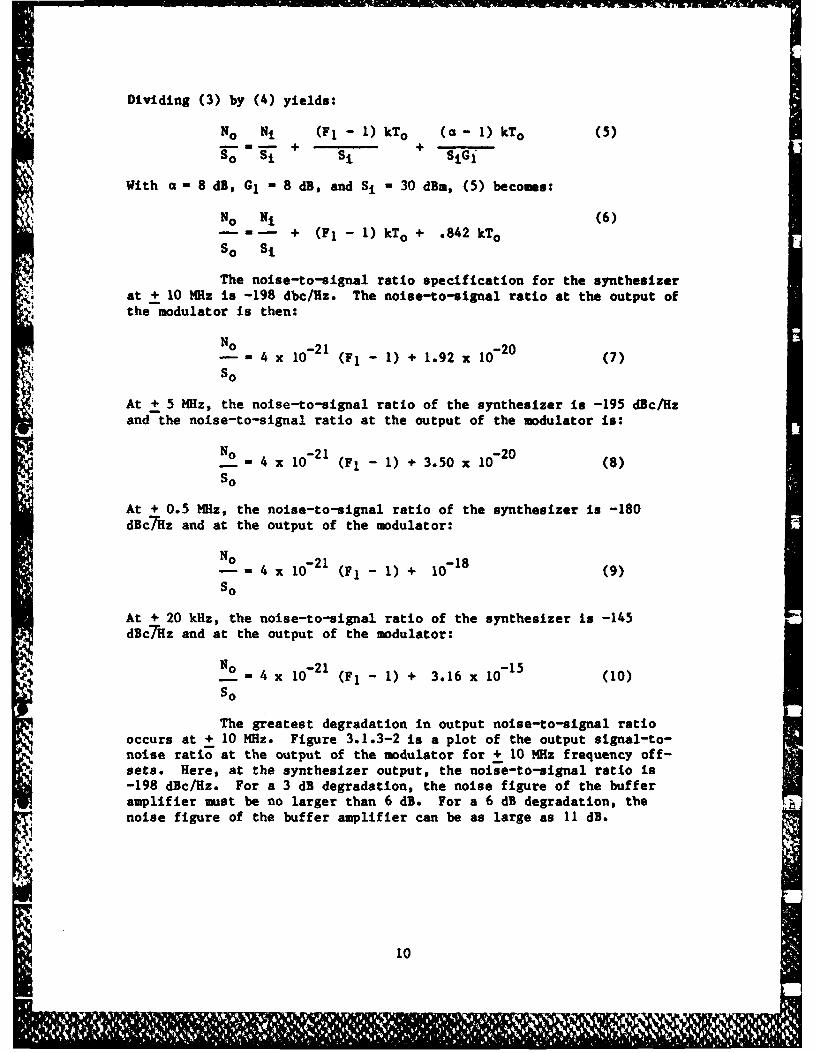
Dividing (3) by (4) yields:
No Ni (F 1 - 1) kTo (a- 1) kTo (5)
- -ri + Si + SiGj
With a - 8 dB, G1 - 8 dB, and Sj - 30 dBm, (5) becomes:
No Ni (6)- - - + (FI - 1) kTo + .842 kToSo Si
The noise-to-signal ratio specification for the synthesizerat + 10 MHz is -198 dbc/Hz. The noise-to-signal ratio at the output ofthe modulator is then:
No -21 -20- 4 x10 (F 1 - 1) + 1.92 x 10(7)So
At + 5 MHz, the noise-to-signal ratio of the synthesizer is -195 dBc/Hzand the noise-to-signal ratio at the output of the modulator is:
N N0 -21 -20(8- - 4 x10 (F 1 - 1) + 3.50 x 10(8)So
At + 0.5 MHz, the noise-to-signal ratio of the synthesizer is -180dBc/Hz and at the output of the modulator:
No M 10-21 0- 18N 4 x (F1 - 1) + 1 (9)
So
At + 20 kHz, the noise-to-signal ratio of the synthesizer is -145dBc7Hz and at the output of the modulator:
No -21 - 1 5
- 4 x 10 (F 1 - 1) + 3.16 x 10 (10)so
The greatest degradation in output noise-to-signal ratiooccurs at + 10 MHz. Figure 3.1.3-2 is a plot of the output signal-to-noise ratio at the output of the modulator for + 10 MHz frequency off-sets. Here, at the synthesizer output, the noise-to-signal ratio is-198 dBc/Hz. For a 3 dB degradation, the noise figure of the bufferamplifier must be no larger than 6 dB. For a 6 dB degradation, thenoise figure of the buffer amplifier can be as large as 11 dB.
10

:69
BUFFER AMPLIFIER NOISE FIGURE VS OUTPUT NOISE-TO-SIGNAL RATIOWITH AN INPUT NOISE-TO-SIGNAL RATIO OF -198 dec/Hz
*4
'119
dc
tz
z -194
U
I0-J-192
-194
-192
.. . .. . .
-190 ...............
0 ...... 2.... 4 .6.8.10.1... BUFE AMPLIFIER. NOISE..FIGURE-...
Figur 3.1.3-2.... Buffer. ..liir.oieFiur.eruOupu Nois....S...a Ratio...........
.... .................. . - I ... ......1. .
.. ... . . . . I . . . . .. . . . . . . . . . . .

Table 3.1.3-1 shows the degradation in output noise-to-signal rati6 caused by the modulator at the four specified frequencyoffsets for both a 6 dB and 11 dB buffer amplifier noise figure.
Table 3.1.3-1 N/S Degradation/diB.
Buffer AmplifierNoise Figure/dB + 20 K~z 0.5 M1 z + 5 M S 101 1
6 0 0.1 1.7 3
11 0 0.2 4.1 6
3.2 Modulator Design
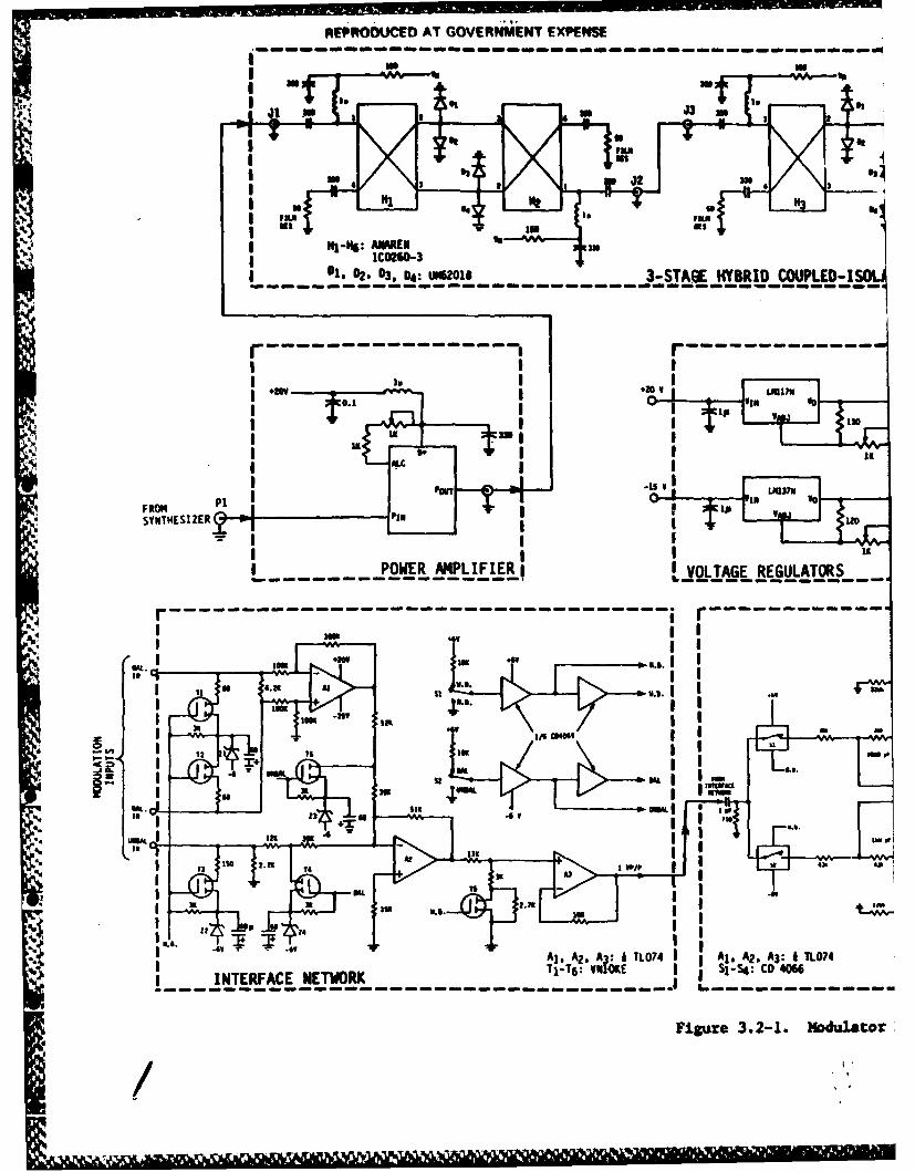
Figure 3.1-1 is a block diagram of the feasibility modula-tor model. Figure 3.2-1 is a detailed schematic of the modulator. Theindividual blocks and their schematic representations are described inthis section.
3.2.1 Buffer Amplifier
The buffer amplifier located at the modulator's RF inputport provides an 8 dB nominal gain across the 225-400 MHz band.
It was shown in paragraph 3.1.1 that 8 dB of attenuation isrequired for modulation. To overcome this loss the buffer amplifiermust have a gain of 8 dB.
Because the modulator must present a JSWR of <2:1 to thesynthesizer the modulator's input impedance must be well controlled.The buffer amplifier isolates the PIN diode attenuator's input VSWRvariations as the attenuator impresses amplitude modulation onto the RFcarrier.
12
I1 x~*
REPRODUCED AT GOVERNMENT EXPENSE
J38
usi
as SI
L~ 01 02- m3, 0,s WN182±m m mm 3-STAGE HYBRID COUPLED-I
rs mm - mm - - mm mm m- --- rmimii -m - m - mm -
IK 1,11 1 1 30
"I I ls 1
14LC153 LI15 vP i0 in So
FRO" n _______p___
SYNTHESIZER 2 ' 2
IPOWER AMPLIFIERI I VOLTAGE REGULATORS
mm m m m m mm m m m m m -m m m nm m m -mm. ----------- r - - -mm-- - m mm - -
I 3
sk I
12 1 s o
'a1
InI
I ILI
Al. A2. A3:* iTL074 I g Al. A2.A3: tTLO74INTERFACE NETWORKT-T:VOE I SS 4 CD06
Figure 3.2-1. Modulator

R4 I
SE Sus
N4 HS N6f
PLED-ISOLATED PIN DIODE ATTENUATOR - -
----------- ----- -------------
I I4
IK V I
'NI S FORWARD POWER DETECTORIN s
LATORS - -I ----- -- -- -- --- --- - - - - - -- -- -- -- -- -- ----
ALC FROPOWER DETECTOR
?IIN
*gs 1007 nI.
IwoIIBAND SHPNGNTWR ECOTOLAPLFERATEUTO RIE
Modulato Detailed Sceati
13133SNdPOI~bNT3O 4. INflO~3

REPRODUCED AT GOVERNMENT EXPENSE
Paragraph 3.1.3 analyzes the degradation of the synthesiznoise performance caused by the noise figure of a loading device. Thsynthesizer S/N degradation goal and requirement along with therequired modulator noise figure is derived in paragraph 3.1.3 and shoin Table 3.2.1-1.
Table 3.2.1-1. N/S Degradation/dB
Buffer Amplifier fo + 10 MHzNoise _Figure/dB
6 3
11 6
The maximum allowable synthesizer N/S degradation of 6 diplaces a limit on the buffer amplifier's noise figure of 11 dB.
The buffer amplifier used in the deliverable, feasibilit,model was an Accrian UHF FET amplifier subassembly model PB4013.Amplitude and return loss for this packaged device is shown in Figuri3.2-1. The device's maximum gain of 18 dB is reduced by amplifierautomatic level control (ALC); a dc voltage applied to the FET gate.The required 8 dB amplifier gain was achieved by fixing the ALC bias10 volts. The measured amplifier noise figure is 11 dB. The worstcase measured input VSWR occurs at 225 MHz as shown in Figure 3.2.1-where an input return loss of 11.5 dB is shown at this frequency. TVSWR is found by:
VSWR - RL+1RL - 1
where RL is the return loss. Hence RL - 14.13 (11.5 dB) and
15.13VSWR - 15:13 - 1.15:1
The amplifier was case mounted to a convection cooled he
sink which serves as the mechanical base for the modulator. Long teoperation of the amplifier showed no appreciable rise in case tem-perature for the approximately 30 watts of dc power dissipated in tb
buffer amplifier.
The amplifier input/output pins are mounted to a micros
PC board which in turn is coupled to the modulator's input port and ,electronically controlled attenuator via coaxial cables.
14

SS01 NUA13I
] i -- !
.t1 -__ ! ... I | ',.
0 in cu
NN
C1 "r x / i' -
w++
I Ia.
-•F 1 6 -1-i m
-x
IIl
S @~ e1 I IM
w I g
N -
N 0 g
is is -
+ + 1I
(mLO 8i340d) NIV9
15
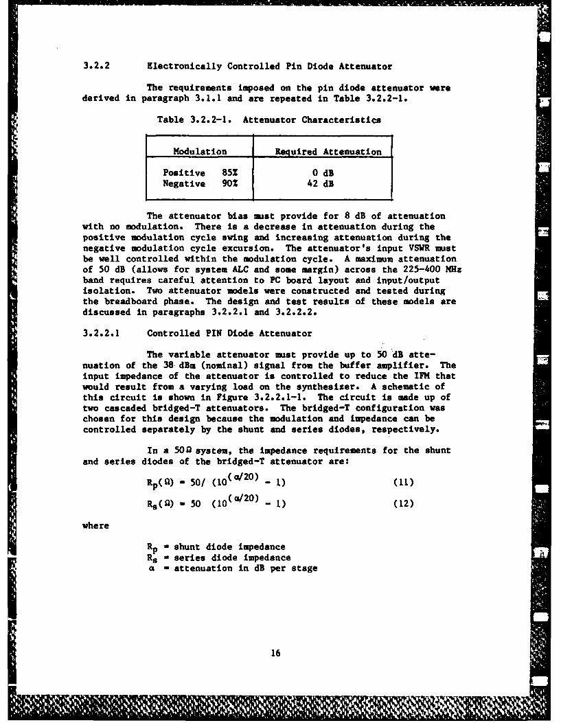
3.2.2 Electronically Controlled Pin Diode Attenuator
The requirements imposed on the pin diode attenuator werederived in paragraph 3.1.1 and are repeated in Table 3.2.2-1.
Table 3.2.2-1. Attenuator Characteristics
Modulation Required Attenuation
Positive 852 0 dBNegative 902 42 dB
The attenuator bias must provide for 8 dB of attenuationwith no modulation. There is a decrease in attenuation during thepositive modulation cycle swing and increasing attenuation during thenegative modulation cycle excursion. The attenuator's input VSWR mustbe well controlled within the modulation cycle. A maximum attenuationof 50 dB (allows for system ALC and some margin) across the 225-400 MHzband requires careful attention to PC board layout and input/outputisolation. Two attenuator models were constructed and tested duringthe breadboard phase. The design and test results of these models arediscussed in paragraphs 3.2.2.1 and 3.2.2.2.
3.2.2.1 Controlled PIN Diode Attenuator
The variable attenuator mst provide up to 50 dB atte-nuation of the 38 dBm (nominal) signal from the buffer amplifier. Theinput impedance of the attenuator is controlled to reduce the IFM thatwould result from a varying load on the synthesizer. A schematic ofthis circuit is shown in Figure 3.2.2.1-1. The circuit is made up oftwo cascaded bridged-T attenuators. The bridged-T configuration waschosen for this design because the modulation and impedance can becontrolled separately by the shunt and series diodes, respectively.
In a 509 system, the impedance requirements for the shunt
and series diodes of the bridged-T attenuator are:
Rp(a) - 50/ (10o( a/ 20) _ 1) (11)
- 50 (10(a/20) - 1) (12)
where
Rp - shunt diode impedanceRs - series diode impedancea - attenuation in dB per stage
16

CL)
HI,
CDiat- nIwI
Q0LAl
U.p
171
The system nust provide two control loops for the PIN diode
attenuator. The first control loop varies the current through theshunt diodes as a function of the modulation and the ALC signals. Thesecond control loop varies the current through the series diodes as afunction of the impedance detector signals.
The modulation bandwidth requires that the shunt diodes in
the modulator loop operate at frequencies up to 25 KHz. The impedanceloop tracks the modulation and therefore, the series diodes mustoperate at least a factor of ten higher in frequency, or up to 250 kHz.At these frequencies, the effect of minority carrier lifetime must beconsidered. The minority carrier lifetime must be significantlyshorter than the period of the highest control signal frequency andsignificantly longer than the period of the lowest RF frequency. Therequirements for the shunt and series diodes are as follows:
A) Shunt diode requires a minority carrier lifetime shorterthan 1/25 KHz or 40 microseconds and longer than1/225 MHz or 4.4 nanoseconds.
B) Series diodes require a minority carrier lifetime
shorter than 1/250 KHz or 4.0 microseconds and longerthan 1/225 MHz or 4.4 nanoseconds.
This shows that the requirements for the series diodes are
the most demanding. The minority carrier lifetime for the seriesdiodes should be around 400 nanoseconds.
The PIN diode attenuator of Figure 3.2.2.1-1 was carefullyfabricated and tested. The circuit was constructed on a di-clad lami-nated dielectric PC board (Keene Di-Clad 527) using microstripconstruction techniques. The 50 ohm resistors used were of thin filmberillia ceramic (pyrofilm 300-10-3) construction. The PIN diodesshown in the figure were PILL packages (HP5082-3340) mounted in a shuntconfiguration for microstrip PC board construction. The bypass capaci-tors (330 pF) were standard chip capacitors also intended formicrostrip installation.
Table 3.2.2.1-1 lists the test results taken from a networkanalyzer. The control levels (simulating modulation and impedanceloops) were dc voltages.
18

Table 3.2.2.1-1. PIN Diode Attenuator Characteristics
Frequency Attenuation Input Control Level(MHz) (d) VSWR (Vdc)
225 2.1 2.6 0* 225 10.2 2.1 4.46
225 22.1 1.5 5.94225 28.6 1.3 6.31225 52.4 1.12 10
400 2.3 2.43 0400 9.6 1.98 4.46400 20.1 1.43 5.94400 25.3 1.23 6.31400 39.6 1.06 10
The tabulated results show a marginal attenuation level atthe 400 MHz frequency while the VSWR at the low frequency end of theband was greater than required (VSWR <2.1).
A subsequent investigation showed the degraded VSWR ste mmedfrom approximately 1.5 pF of stray capacitance across the 50 ohm powerresistors. Modeling the circuit on COMPACT and inserting theresistor's stray capacity into the computer program simulation circuitconfirmed the results of Table 3.2.2.1-1.
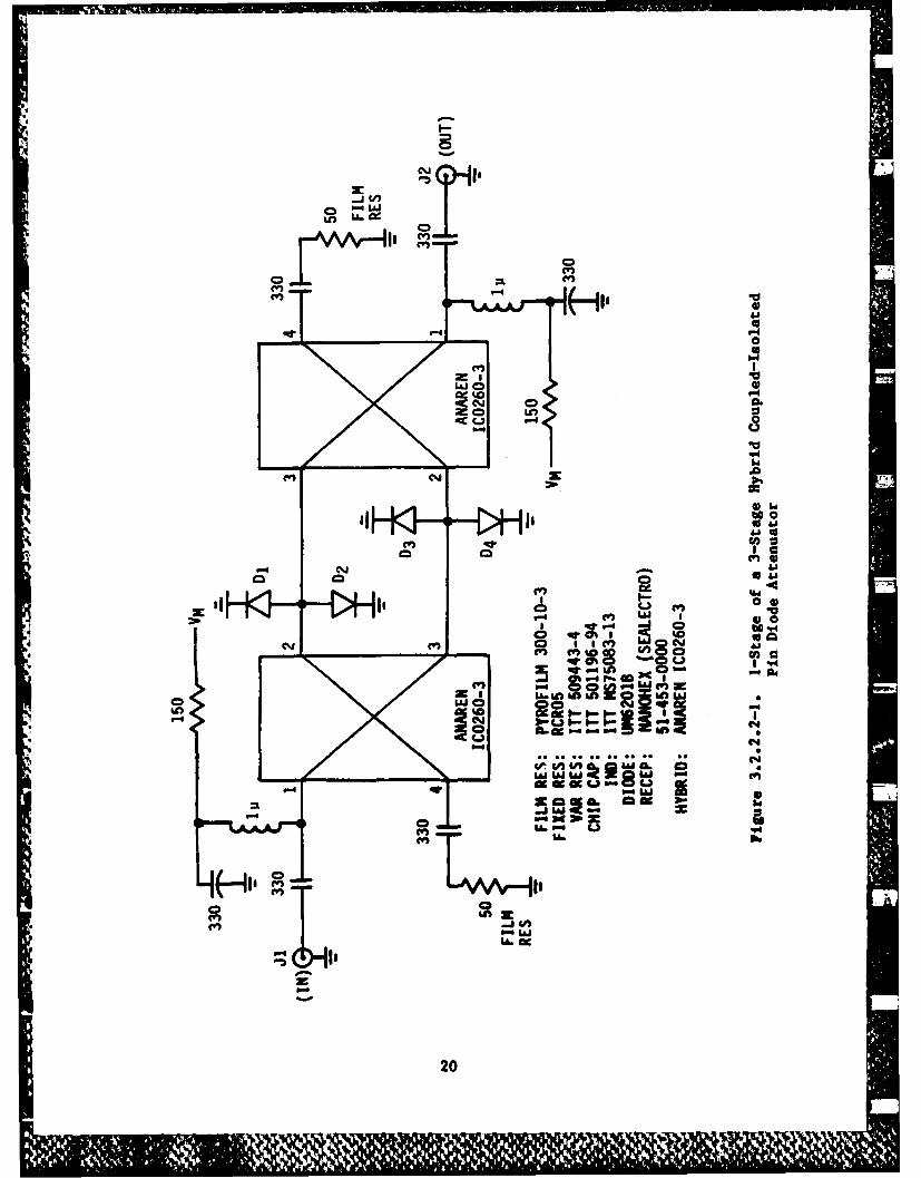
3.2.2.2 Hybrid Coupled-Isolated PIN Diode Attenuator
Figure 3.2.2.2-1 is a detailed schematic of one stage of athree stage hybrid coupled-isolated PIN diode attenuator. The purposeof the hybrid coupler is to isolate the input port (No. 1) from theoutput ports (Nos. 2 and 3). Port No. 4 is terminated in the coupler'scharacteristic impedance and absorbs any power mismatch introduced bythe loads at ports 2 and 3. The impedance variations of the PIN diodesand the stray capacity of the 50 ohm power resistor (discussed inparagraph 3.2.2.1) are isolated from the input port resulting in anexcellent attenuator input VSWR across the frequency band.
A desirable characteristic of the hybrid attenuator is theisolation of the PIN diode impedance variation from the source. This
permits control of the diodes in only one control loop (ALC) instead ofthe two loops (impedance and ALC). The dc bias for the PIN diodes isfed into the input port (No. 1) permiting the diodes to terminate theoutput ports (Nos. 2 and 3) directly rather than through a dc blockingcapacitor. The breadboard and subsequent feasibility model used an
ANAREN (ICO 260-3) 90 degree-hybrid coupler.
19
HI
z;j (4
4 lEl
-2 1
X '44
00
CID en
-4 j CD -
at I, a m0~ n SO 41
m4 0-4 %
CV) A48
3 4
CA W* "aC
CI'.
CV)
zz
20

A three stage attenuator, shown in Figure 3.2-1, wasconstructed. The attenuation and reflection coefficient of the threestage attenuator as a function of frequency are shown in Figure3.2.2.2-2. This network analyzer plot shows the attenuation (S21)across the 225-400 MHz band to range from -09 dB to -1.5 dB for zerovolt modulation level while the maximum attenuation shows a range of-65 to -62 dB at the same 'requencies for a 2 Vdc input level (VM inFigure 3.2.2.2-1). A constant attenuation level across the frequencyband is not critical to modulator performance due to error correctionby the system ALC. The minimum and maximum attenuation of 1.5 dB and62 dB respectively are more than adequate for the modulator's percen-tage modulation requirements.
The input VSWR across the band is calculated, as before,from the input reflection coefficient. The worst case input VSWRcalculated from a 12 dB reflection coefficient (SI) at 360 MHz is then1.13:1.
The attenuation as a function of drive (modulation) voltageof the 3 stage attenuator is plotted in Figure 3.2.2.2-3. It has goodlinearity over the 2 to 40 dB attenuation range.
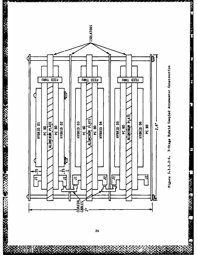
Construction of the attenuator, as discussed previously, iscritical. Figure 3.2.2.2-4 is a drawing of the 3-stage attenuatorshowing isolation (aluminum plates) between PIN diodes (DI/D2 and D3/D4in Figure 3.2.2.2-1) and also between the 3 stages. The nano-hexinput/output connectors and miniature 50 ohm coaxial cable are used.The construction of the attenuator permits ease of installation viacard guides mounted on the modulator's side walls (see mechanical con-siderations in paragraph 3.2.6).
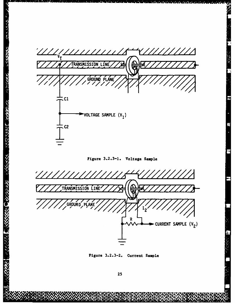
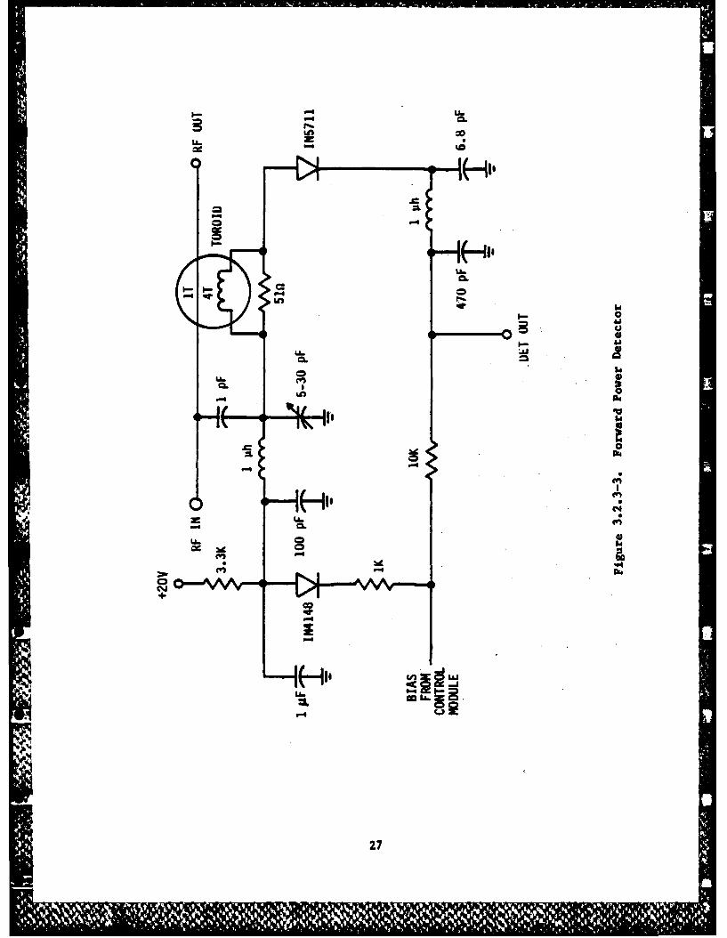
3.2.3 Forward Power Detector
A power level detector provides information for the atte-nuator control circuit to adjust modulation depth and provide automaticlevel control (ALC).
Detectors sample the voltage and the current on atransmission line as shown in Figure 3.2.3-1. The voltage sample canbe derived from either a resistive or capacitive voltage divider bet-ween the transmission line and ground. In the 225-400 MHz band, acapacitive divider is preferred because it is less susceptable to straycapacitance than a resistive divider. As long as the voltage sampleoutput is not loaded, it has the same phase as the line voltage. Themagnitude of the sample voltage is
ClV1 - VT, where VT is the line voltage.
C1 + C2
The current is sampled with a toroidal transformer asillustrated in Figure 3.2.3-2.
21
5 4 lip

Iq I9 Im T
LI..
'PA5
7 mm
13I- M 20WStrI
00)
T ti
A 1 .54
TN
Lfl Im SO
*p :, 7 h

38
7- MODULATION 7-
24-
323
28~
LizY
.4c
-i
F0
00001-100
10000
00
0 'o =50
0=0
<A
,-.0 01-1 1-
ool 10.0e--I'a
kn Ln C
e--" ,Oo ,O 4
/0010
24.
VOTAG APLE ( 1
C2
Figure 3.2.3-1. Voltage Sample
///CURRENT SAPL (V2)N
Figure 3.2.3-2. Current Sample
25
1%I *111 11
The current in the secondary winding is
12 - IT/N, where 12 is the secondary current, N isturns ratio, and IT is the primary current.
When this current is loaded by a resistor, R, the voltageacross this resistor is approximately
V2 - 12R - IT(R/N)
V2 is a voltage proportional to the current in the transmission lineand in phase, or 180" out of phase, depending on the winding sense ofthe transformer. Figure 3.2.3-3 is a schematic of a completed forwardpower detector.
The operation of the forward power detector is straightforward. The voltage and current samples are equal when the impedance(Z) is 50 0. The two samples are added together as phasors at RF. Thetransformer is phased so that voltages add when driving 50 2. The out-put voltage is therefore proportional to the square root of the forwardpower on the line. The square root function is a result of the factthat the voltage and current samples are added and not multiplied.This is necessary to provide the modulation information to the controlcircuit that supplies the current to the attenuator's shunt diodes.The dc component of the detector output which is a measure of thecarrier level provides an automatic level control (ALC) signal to themodulator.
The detector is located between the modulator and the 50ohm load (antenna). The bias voltage is supplied by the control moduleto pre-bias the 1N5711 detector diode. The detected output which issent to the control module consists of a dc level, corresponding to theRF carrier level, for system ALC and the audio modulation envelope toaid in maintaining low distortion in its modulated RF output signal.
Tests were conducted on the detector module with a 6 wattPEP RF input drive and a modulating frequency varying from 300 Hz to 25kHz. The detected output level consisted of a 300 uV P-P audio enve-lope riding on an 800 mV dc voltage. The corresponding carrier dLstor-tion was less than 5 percent while the input VSWR was noted to be1.03:1.
The foregoing test showed that performance of the detectorjwas satisfactory.
26
LLn
-
Id.boo
0 119en
CD.
V) Z8 0
27d
'.4' 1 1

3.2.4 Interface and Control Circuits
Requirements of the interface, band shaping, and controlci cuits are discussed in the following paragraphs.
3.2.4.1 Interface Module
The interface module converts wide and narrowband modu-lating signals to a constant level for driving the control module. Inaddition to level control of the input signals the module providesboth a balanced and an unbalanced input port, front panel mode selec-tion switching, port input impedance control and output port isolation.These requirements are sumrized in Table 3.2.4.1-1.
Table 3.2.4.1-1. Modulation Requirements
Input Mode _
Parameter Balanced Unbalanced Units
Input Impedance:Narrowband (300 to 3500 Hz) 150 + 30 150 + 30 OhmsWideband (300 to 2500 Hz) 6 + 0.6 2 _ 0.2 K Ohms
Input Voltage:Narrowband 1.4 1.4 VrmsWideband 12 12 V p-p
The interface module converts the different input voltagelevels (4 and 12V p-p) to a constant 1 volt p-p drive level to thecontrol module to maintain a constant modulation percentage.
Figure 3.2.4.1-1 is a detailed schematic of the interfacenetwork module. The figure shows the balanced and unbalanced inputports terminated in the required input impedances (per table3.2.4.1-1), via the T1/T2 and T3 FET stages, conversion of the balancedinput port to an unbalance mode through amplifier Al, and combiningboth balanced and unbalanced modes in summing amplifier A2. FET T6 isenabled in the wideband operational mode to assure a constant modu-lating signal level output regardless of input mode. Amplifier A4 isan output buffer which provides a low impedance drive to the bandshaping network. FIT's T4 and T5 provide port isolation to the unusedport. FIT T6 is enabled by the selection of the unbalanced mode whichgrounds the output of Al, the balanced input port, thus isolatingsignals coupled into the modulator's balanced port. FET T4 is enabledin the balanced mode to produce similar results. Measurements show
greater than 60 dB of input port isolation is obtained in this manner.A CD4069 integrated circuit provides the wideband/narowband gates tothe switching FIT stages (VNIOLE). The operational modes (wideband/narrowband - balanced/unbalanced) are front panel controlled by panelmounted toggle switches. Zener diodes, Z1 through Z4, bias switchingFET stages TI through T5 to prevent high level modulation swingsturning the FET stages to their on condition. Module testing showed:
28
411t -

B ~ I
a-W
at'-,~~~~ - A2 U0 11
i>
3d 3
Ik- N44
1-4-
00
29S

* The input voltages are converted to a constant 1 V p-poutput level.
* The input impedances are within tolerance.
" A port to port isolation of 60 dB.
" Signal balance Is preserved at the balanced input.
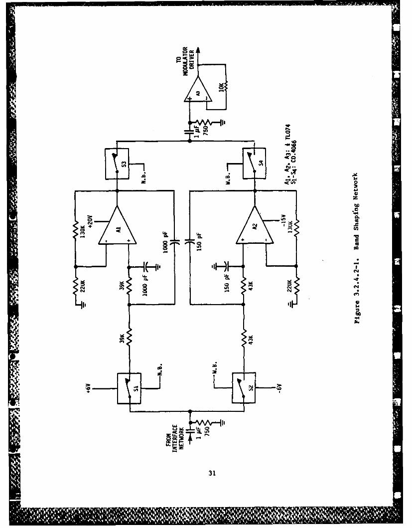
3.2.4.2 Band Shaping Network
Figure 3.2.4.2-1 shows the band shaping network schematic.The module contains the 2 pole high pass and 2 pole low pass filtersrequired to meet the band shaping requirements.
The high-pass filtering for a 300 lz lower 3 dB frequencyis provided by the input/output C-I (I pf-750 ohm) networks. The low-pass filtering for either a 3500 Hz or a 25 kHz upper 3 dB cutoff fre-quency, is provided by active two-pole filters. Operational amplifierAl is a 3500 Hz low pass filter while A2 is a 25 klz low pass cutofffilter. Filter path gains are identical, thus preserving the modu-lating signal level. Switches S1 through S4 (CD4066 integratedcircuit), controlled by the selected operational mode, choose theappropriate low pass filter. Module test results show:
" The cutoff frequencies to be within +5% of the requiredvalue shown in Table 3.2.4.1-1.
" The frequency roll-off is 9 dB per octave or greater atfrequencies below the lower cutoff frequency (300 Hz)and above the upper cutoff frequencies (3.5 kHz and25 kHz).
* Input signals of 6 V p-p can be tolerated at the input
port. This results in a desirable margin for the nomi-nal 1 V p-p input modulation level.
3.2.4.3 Modulation/ALC Control
Modulation and automatic level control in the EMIC EnhancedConstant "Z" Modulator are provided in the same loop. A schematic ofthe control circuit for this loop is shown in Figure 3.2.4.3-1. Thesignal from the power detector is a voltage that is a function of thesquare root of the forward power. This voltage contains the modulationand a dc level representing the average power. This circuit can beanalyzed by considering it to be a negative feedback linear amplifier.Applying the principle of superposition, the loop is set up with nomodulation first to set the dc bias and then the modulation is appliedand adjusted for the proper percent modulation.
30
I',
L-.
-IC
C-'C
LA.~
26 CLUd
"4
+
LLS
a. -*.cz0
In -CwU4C~
31a,.

LU
LL d
CJj45.
US.LL. Cc 0Cie5
CD >-
cS.'
a I.C*4 0
0 0 So
0W 01,
C54
0A
CD c-
< = - to 5-
32

The control module breadboard test results showed a fre-quency response of 230 kHz and a peak modulating input drive capabilityof 10 volts. The balanced FET drivers (IRF 122/9120) can reliablysource and sink several amperes of drive current without heatsinks.
The >200 kHz frequency response is adequate to process the25 kHz input modulating signals while the I volt peak modulating drivesignals are well within the operational amplifiers (TL074) range. The39 pF feedback capacitor enhances the drive linearity. A measureddistortion of less than 0.5 percent for this stand-alone circuit iswell within the modulator's overall distortion requirement.
The 50 kilohm potentiometer which is located on the frontpanel controls the ALC level. Provisions have been made for anoptional power amplifier (see Figure 3.1-1) to be inserted between theattenuator and the power detector.
3.2.5 Mechanical Requirements
The constant Z modulator is self-contained in an aluminumhousing mounted on an aluminum heatsink. Figure 3.2.5-1 is a pictureof the complete modulator housing, the base heatsink, the input/outputconnectors and the front panel hardware.
Figure 3.2.5-2 is a detailed drawing of the assembled modu-lator showing the front panel assembly and the module locations. Theamplifier is horizontally mounted to the modulator's base heatsink.Each module, except the RF amplifier, is card guide mounted for ease ofmaintenance. The front panel contains mode switches, the ALC control,and the modulation input ports. The RF connectors interface the modu-lator between the synthesizer (RF IN) and the antenna (RF OUT). Theoptional power amplifier (see Figure 3.1-1) would replace the cablingmarked PA. The system test point (see Figure 3.2.4.3-1) permits exami-nation of the modulating signal's characteristics such as amplitude,pass band and stop band parameters.
Operationally the packaged modulator showed the following:
0 The amplifier heatsink was adequate to dissipate the
25-30 watts of dc power.
A3

Figure 3.2.5-1. Modulator Enclosure
34

* The PIN diodes mounted in the firat stage of the atte-nuator registered a high heat rise due to inadequateheatsinking. This stage attenuates the 6 watt carrierlevel prior to further attenuation by the succeedingstages. The heatsink for these glass diodes (unitrode6200B) consists of a 1/8 inch aluminum plate connectedto the aluminum sidewalls through the metal card guides.Modulator testing showed that the overheating PIN diodesresulted in increased PIN diode resistance which ultima-tely decreased the modulation percentage. The modula-tor's final tests were conducted utilizing a small benchfan cooling the housing's 'hot spot'.
The RF isolation through the modulator was adequate as
was the power supply bypasses.
3.2.6 System Testing
Breadboard system tests resulted in the replacement of theHP5082-3340 shunt mounted PIN diodes due to a carrer life time inade-quacy. The typical carrier lifetime of 400 nanoseconds (HP data sheetparameter) was found to be deficient when the modulating frequency wasgreater than 10 kHz. A PIN diode with a typical carrier lifetime of800 nanosecodns (UM6200B) was substituted for the HP device. Thisresulted in excellent dynamic results. The attenuator was retested onthe network analyzer for swept frequency insertion loss and input VSWRas a function of modulating voltage. The measured results were similarto the responses of Figure 3.2.2.2-2 taken with the HP diodes.
System test results are discussed in Section 4 of thisreport.
73
4

41
'Ir
Section 4
SYSTEM TESTS
4.1 Modulator Test Results
System testing, including the final test, covered thesystem parameters shown earlier in Table 1.4-1. The final test resultsare given in Table 4.1-1 and each parameter is discussed in detail inthis section.
4.1.1 Frequency Range
The specified 225 to 400 MHz frequency range requirementwas easily met. The actual usuable range extends from 210 MHz to450 MHz, being restricted on the low frequency band edge by the modula-tion distortion arising from the PIN diode minority carrier lifetimeand on the high band edge by the buffer amplifier's frequency response.
4.1.2 Input Power
The input power handling capability exceeded the required30-33 dBm range by a comfortable margin of + 3 dB minimum. Te-2ingover the frequency range showed the systemaLC capable of maintainingthe required modulation percentage over an input power as low as 0.25watts (+24 dBm) to as large as 6 watts (+38 dBm). The ihput powerlevel was not increased beyond the 6 watt limit due to possible bufferamplifier permanent degradation.
4.1.3 Input/Output Impedance
The modulator's nominal 50 ohm impedance level showed aVSWR of 1.4:1 maximum over the operating frequency range. The 1.4:1VSWR represents a resistive impedance level of 35 or 70 ohms. Themeasurement was made with audio modulation. With a +85, -90 percentmodulation at the modulator the measured incidental AM at the output ofthe synthesizer was 0.2%. This modulation isolation is necessary toprevent incidental frequency modulation of the synthesizer sourcedrive.
4.1.4 Insertion Loss
The measured insertion loss was less than 2 dB.
37
JU'

UN
0 0 a
C4 n 04 m 00 o 94%a0
Al P3 m i0*
2 01 - -. IWI0
~~~~~~ 0 cc* * "~N0ON en On ". V4t ~O N A 1 a u1l 04% it4
U % 0 * 1 H tq +1+1%c 1 en 00 A -l %O -002 -
cc go000i
000
o F
PIV -
orl a N4 C0 9 0tvc
-b P-44%
"U 5.4 11 "4 Wl $ 4
"4 0 &A 00 0000V~41 60 61. tu. N 401%Na-a S Is 2 -
'6d a U 1 0
S 01 ~ ha N ~30
-z 0
4.1.5 Output Signal-to-Noise (S/N) Degradation
The output S/N degradation was carried out by measuring themodulator's noise figure. Table 3.1.3-1 relates the device noisefigure to the synthesizer S/N degradation parameter while paragraph3.1.3 derives the mathematics for the table.
The modulator's noise figure, measured at 246, 312, and 360MHz, ranges from 10.8 to 11 dB. The calculated S/N degradation wasshown to be <6 dB at the measured low, mid, and high band frequencyranges.
4.1.6 Incidental FM (IFM)
The incidental FM requirement of <2.5 kHz was demonstratedby monitoring the modulated carrier with the modulator driven by the -
low noise synthesizer. The measured frequency deviation of 1.25 kHzmaximum resulted from responses taken at 10 MHz increments over thesynthesizers 225-400 MHz frequency range. The 1.25 kHz represents a0.0003 percent induced frequency error in the synthesizer's selectedfrequency.
4.1.7 Modulation Bandwidth
The nominal 300 to 3500 Hz narrowband and 300 to 2500 Hzwideband bandwidth requirements were slightly exceeded as shown in thetable. These non-critical responses are governed by the low and highpass filter sections located on the band shaping module. Judiciouscomponent selection (or variable resistors) would be necessary to meetthe exact frequency responses as stated.
In addition the SOW also required stopband responses of6 dB/octave minimum outside the nominal pass bands shown in Table4.1-1. Measured stop band results taken at octave increments above andbelow the pass bands show a >8 dB roll off characteristic.
4.1.8 Modulation Capability
The +85%, -90% minimum modulation capabilty at thenarrow and wideband voltage levels shown were met in the narrowbandmodulation mode but were 0.3% under the minimum in the wideband mode.
This deficiency is easily corrected by initiation of the
front panel ALC control. During the final tests the under-modulationcondition was found to exist during the exercise of the wideband-balanced input modulation mode; thus correcting the level by the ALCpotentiometer adjustment would influence the previous modulation modetest results and this corrective action was not taken.
39
N Z \
4.1.9 Distortion
Measured distortion levels of the modulated RF carrier( kHz modulation) showing 2.5 percent maximum over the RF frequencyband were well under the 52 goal, 10% max criteria. This parameter islinked to the carrier's modulation percentage and modulator insertionloss. Care must be taken in the set-up of the ALC control to preventan over modulation condition derived from large (>15 V p-p) input modu-lating signals.
4.1.10 Modulation Input Impedance
The modulation input impedances at the narrow and widebandports were met except in the wideband-balanced operational mode.
These non-critical parameters are set by the input shuntresistors loading the input ports. Careful selection of the 6.2K ohmresistor in the balanced input port (see Figure 3.2.4.1-1) would berequired to meet the 6000 ohm nominal input impedance.
4.2 Test Data Summary
The measured data of Table 4.1-1 shows most of the testrequirements being met. In the case of the critical parameters (inputpower, insertion loss, IFM, S/N degradation, distortion, and modulationcapability) only the modulation requirements of the videband-balancedmode were compromised and then only by 0.3%. All non-critical parame-ters except the wideband-balanced modulation input impedance were met.As discussed in paragraph 4.1.11 action could be taken to guarantee theimpedance to be within specification as well.
In summary, the final testing of the modulator resulted inexcellent correlation with the program's stated goals andspecifications.
40
Section 5
CONCLUSIONS AND RECOMMENDATIONS
5.1 Conclusions
The program goal of the EMC Enhanced Constant "Z" Modulatorwas the development of an amplitude modulator operating in the UHFregion as a companion modulation scheme for a low phase noise frequencyhopping synthesizer presently under development at ITT-A/OD.
The 12 month RADC sponsored program encompassed research,breadboard and feasibility model stages that resulted in accomplish-ment of the SOW goals and specifications. The program drew uponresults from a previous ITT-A/OD sponsored IR&D program investigatingthe amplitude modulation scheme eventually employed in the EECZM.
5.2 Recommendations
Reconmendations for a modulator follow-on study include:
0 Repackaging of the electronic attenuator to eliminatethe input stage PIN diode 'hot spot'. This task couldbe accomplished by testing various 'shunt' type diodessimilar in configuration to the HP5082-3340 icrostrippower switching diodes or by designing a more optimumheatsink configuration for the presently used UnitrodeUM6200B diodes.
* Further development of a low noise figure input bufferamplifier to reduce the synthesizer S/N degradation tomeet the 3 dB goal.
0 Conduct environment testing on the modulator in areas ofvibration, shock, temperature and altitude to determinecompliance with NIL-standard requirements.
41
UElm=

Section 6
APPENDIX
This section Includes the following vendor data sheets.
" Unitrode UM6200B PIN diode.
" Hewlett Packard HP5082-3340 uicrostrip PIN diode.
" ANAREN 1C0260-3 3 dB, 90* hybrid coupler.
A-1
PIN DIODE UM6000 SERIESUM6200 SERIESUM6600 SERIES
Features" Capacitance specified as low as 0.4 pF (UM6600)" Resistance specified as low as 0.4Q (UM6200)" ltage ratings to 1000V" Power dissipation to 6W
DescriptionThese series of PIN diodes are designed cessfully in switches in which low insertion
for applications requiring small package size loss at low bias current is required.and moderate average power handling capa- The "A" style package for this series is thebility. The low capacitance of the UM6000 smallest Unitrode PIN diode package. It hasand UM6600 allows them to be used as series been used successfully in many microwaveswitching elements to 1 GHz. The low resis- applications using coaxial, microstrip, andtance of the UM6200 is useful in applications stripline techniques at frequencies beyondwhere forward bias current must be mini- X-Band. The "B" and "E" style, leaded pack-mized. ages offer the highest available power dissi-
Because of its thick I-region width and pation for a package this small. They havelong lifetime the UM6000 and UM6600 have been used extensively as series switch ele-been used in distortion sensitive and high ments in microstrip circuits. The "C" stylepeak power applications, including receiver package duplicates the physical outlineprotectors, TACAN, and IFF equipment. Their available in conventional ceramic-metallow capacitance allows them to be useful as packages but incorporates the many reliabil-attenuator diodes at frequencies greater ity advantages of the Unitrode construction.than I GHz. The UM6200 has been used suc-.
MAXIMUM RATINGS
Average Power Dissipation and Thermal Resistance Ratings
Package Condition UMI 1200P0 0 PO 8
A&C 25"C Pin Temperature 6W 25"C1W 4W 37.5"C/WB&E (Axial Leads) '/a in. Total Lead Length to 2.5W 60"C/W 2.0W 75"C/W
(12.7mm) to 25"C ContactB&E (Axial Leads) Free Air 0.5W - 0.5W -
Peak Power Dissipation Rating
Al akae s Pulse (Single) UM6000 - 25 KW UM6600 - 13KAll ackaes at 25 C Ambient IUM6200 -10KW I
SOperating and Storage Temperature Range: - 65"C to + 175"C
I A-2

j UM6000 UM6200 UM6600Voltage Ratings (25*C)
Reverse VoltageTye(VM) - VoltsTye(11% = 10 JAA)__ _ _ _ _ __ _ _ _ _ _ _ _ _ _ _
100y UM6001 UM6201 UM6601200V UM6002 UM6202 UM6602400V -UM6204
600V UM6006 -UM6606
1OQOV UM6010 UM6610
Electrical Specifications (250C)
Test Symbol UM6600 UM6000 UM6200 ConditionsTotal Capacitance (Max) CT 0.4 pF 0.5 pF 1.1 pF OV, I Gl~zSeries Resistance (Max) Rs 2.52 1.72 0.42 100 mA, 1 GHzParallel Resistance (Min) R, 10 KQ 15 KQ 10 K9 100V, 1 GHzCarrier Lifetime (Min) T 1.0 JAS 1.0 JAS 0.6 us 1, 10 mAReverse Current (Max) 1, 10 A 10 ;iA 10 JAA VI = RatingI-Region Width (Min) W 150 )A 150 Atm 140 yam
TYPICAL SERIES RESISTANCE
FOWRDCRRN DC CHARACTERISTICSFOWR CURRNT FORWARD VOLTAGE VS CURRENT
z
UM6600
LIMI 10mALIM$
',.A I)OA 100@jA IMA lCa IOWA I A
POPRARO CURAINT4
0 0.2~ 0.4 as 0. 1 01.2
-FORWARD VOLTAGE IVI
A-3

UM6000 UM6200 UM6600TYPICAL ApVS VOLTAGE & FREQUENCY
ums6c0Wum6o6UM20
S1000
W 00
1 '0 to.4V0 1 00V-EES.VLAEW
VyR -REVERSE VOLTAGE IV
TYPICAL CAPACITANCE VS VOLTAGE AND FREQUENCY
UMIUS SERIES UM620 SERIES1.5 .
1MHZI M 0Mz
I M* z to 1.0
5MZ.100 MHZI
10 MHz 0
?100 M H1 S
o 0
1 1 0 o 10 00 So1 2 5 10 20 s0 100V,- REVERSE VOLTAGE (V) V EES OTG V
U111hhh111111 SERIESORDERING INSTRUCTIONS
.8 1-11 17
Part numbers of Unitrode PIN diodes consist of the letters 7.UM followed by four digits anid one or two letters. The first
Utwo digits indicate the diode series, the next two digits Z .6-specify the minimum breakdown voltage in hundreds of '
volts. The remaining letters denote the package style. ~-Reverse polarity (anode large end cap) is available for 1 MI M
the C style and denoted by adding second letter R. -
- MHFor Exar"Ple: Lim 6006 IC 0 0I-
* o .31MHz 41 2 S 10 20 so 1oo
V.- REVERSE VOLTAGE (V)
A-4

UM6000 UM6200 UM600
POWER RATING -AXIAL LEADED DIODE
.7ZA ,,
3 -IN
0O 7S loo 1025 ISO 17 5 s Is lo 12 S
tLAD TEMtIRATU0RE C0 LEADOTEM9SRAIUAf 16C
6.W POWER RATING
5 4.W ;7 UM6000 and- 0w - -U 0Series
a. ~UM60-
-50-25 0 25 50 75 100 125 150 175TEMPERATURE (-C) (of one ,mtal pin)
PULSE THERMAL IMPIEDANCE VS PULSE WIDTH~100
Z10
3 2UM20SR
.5 MMS1A IH .2I
IL .02Irv" .01
10i-6 lo-' 10-4 1-1 10-2 10-'
PULSE WIDTH (SEC)
A-5
UM6000 UM6200 UM6600MECHANICAL SPECIFICATIONS
STYLE A STYL E
.01ISus
(2 16)2.411 .97 , = ,
00 (.201 k S+0 1.20!
T ' 12.13) .014 (~I. 021 (11 M . LO
A. 021 1 0
STYLEaLL CATH~ SAN*
CANIAUDGE DOTAG
.225
.064 97 .25
i'24.1 M;; ' (241)
2 12)
. (1 1 1 10104.0T-1421 . W75
00(1.51-27) ,~(23) ?N 01A.'
T 2.3 -1 (1021 (.181 MAX. VoLLOW.121 (3.18) 11l 074 .050 .007 A"09MRI'S 13.921 91A..00 00
A-6

5082-Zd40/41HE LETPIN DIODES FOR STRIPUNE 50-3HEWLET AND MICROSTRIP SWITCHES 02-97iaPAWKR ATTENP !TORS AND UMTERS 50-3/4
5082-3170
Fature FeatresHERMETIC LOW COST TO USE
(5082-3140. 3141, 3170) Desdgned for soa mountinigBROADIAND OPERATION BROADBAND OPERATION
HPC throuigh X-band HP through Ku-banLOW INSERTION LOSS LOW INSERTION COSS
Loue than 0.5 dB to 10 G1W (5082-3140, 3170) Lou than 0.5 d9 to 100CHI (5082-3040, 3340)HIGH ISOLATION LOW DRIVE CURRENT REQUIRED
Greater than 20 dO to010 OH: (5082-3140, 3170) Laos than 20 mA for 20 do isoltdo (5082-3041)PAST SWITCHING/MODULATING PAST SWITCHING MODULATION
5 ns typial (5062-3141) 5 no typloa (50112-3041)LESS DRIVE CURRENT REQUIRED HIGH POWER LIMITING
Less than 20 mA for 20 dB Isolation (506-3141) S0OW peak pulse power (5002.3071)*
Description The HP 5062.3140. -3141 and -3170 are in NP Package,Outline 60. This package is hermetic and can be used for Hi-Rol applications. The HP 5082-3140. -3141 and -3170 are
When forward biased these PIN diodes will appear as current direct mechanical replacements for Outline 61 1with top capvariable resistors in shunt with a 50 ohm transmission line, in plow)s diodes HP 5062-3040, -3041, and -3340The resistance varies between less than 1 ohm at high M VIeY. The only electrical iflerenc is the location offorward bias to greater than 10,000 ohms at zero or reverse thio chip in each package. Except in those few applicatiols,bias. wheore the difference in phase relaionship.i important, theThe HP 5W62-3040, .3046. -3340, -3140 and .3170 are Outline 60 devices can be used as replacemenitpassivated planar devices. The HP 5082-3041, .3071 and The HP 5062.3071 passive limiter chip is functionally.3141 are passivated mesa devices. All of the devices are insa integrated into a 50 ohm transmission line to provide ashunt configuration in stripline packages. These diodes are broadband, linear. low insertion loss transfer characteristicoptimized for good continuity of characteristic impedance for smail signal levels. At higher signal levels self-which allows a continuous transition when used in 50 ohm rectification reduces the diode resistance to provide limitingmicrostrip or stripline circuits. as shown in Figure 6. Limiter parformance is practicallyOf these devices, the HP 5062-3040. -3041, -3046. .3071 independent of temperature over the rated temperatureand -3340 are in HP Package Outline 61. range.
A-7

AppICatIOnsSWITCHES/ArrENUATORS UMITERThese ~ d ode r* designed for applications in microwave and The 5062.3071 limiter module is designed for applicatinnHI-H systms uLong Silineri Or fgmloen Vsnsnvssan telecommunication equipment ECMI receivers distanceline techniques. measuring equipment. radaor receivers. telemtry equiP.Typical circuit fbinctions performted consist of switching, ment. and transponders operating anywhere In theduplexing. multiplexing, leveling. modulating, limiting. or frequency rngle from 500 MIz through 10 GH4a Anasternagain control functions as required in TR switchoLuse do return is required for self bias operation. This do return ismodulators phase shifters. and amplitude modulators ofte pre in the existing circuit. i.e. Jnductiv*l coupledoperating in the frequency range from HIS thog Ku-Sand. antennas. or it can be provided by a A A4 reesinant shunt
transmission line. Selection of a high characteristicThese diodes provide nearly ideal transmission characteris- impedlance for the shunt transmission line affmorbodbndties fromt HF through Ku-Sand. operation. Another easy to reelie d ow eur consists of a
The 5062-3340 and 606-3170 are reverse polarity devices smal diameterire coecdatrht ipeto tekorwith characteristics similar to tWe 5082.3040 and 5062- fild in a microstrip or stripline circuit. A 10 mA forwar
A 3140 respectively. current will actut thPlfddi @$a Shuntswitch proviin
The 5062-3041 and 5062.3141 are recommende for approximately 20 dS of isolation.appliation requiring fast sitching or high frequency a ag Ou ne6modulation of microwave signals. or where the lowet bias am g O t" 6currant for maximum attenuation is required. Ca C1an el"The 60623046 has been developed for high peak pulspowaro handling as required in Til switches for distance The cover channel supplied with each diode should be usedmasurement and TACAM equipmet The l oeffective in balanced striplina circuits in order to provide odminority carrier lifetime provides for low intermiodulAtion ekacti acontinutyfrom the uppertothelowaregroundplatisproductis down to 10 MHlL through the package base metal. Higherordeode itb
excited if this cover is left off or if Poor electrical contact isMere information is available in HP Application NeIL made to the ground plane.lplodes o I ide)a.L~ Sicig The package transmission channel is filled with epoxcy resin
Diodes).which combines a low expansion coefficient with highchemical stability.
Maximum Ratings at T~m -25*CA N N W O , n d N N W -O W-1 - W C 11 1 1 i t 2 ' r '
Puswok Reo. 47A.~~441
Plane DlishademIl) 17WW .33W -, A ' -?i 4Wftk loollim~d~m USWt UW tWW'holklnm Velp IUDV 70V V
A-8
-VI

Electrical Specifications at TA= 250C -Attenuiator DiodesRm- -
ramh Mblnuau Iuwtm Tim -CLmj. CMftymmh Puimp Hiss. Isi. L". mbum tg PAUrn Om Sink 10)- wo m (ad fadi (W
A cgr, Anamd W0 as5 ?.5 4
mod. r 20 Mt 1.5 Is151-!Qftif*ds 211 0 15 I 4W~ 3W
11M.. . Coot Fm . .211 0 .5 1P is 1320 1.0 1.5 100
W -' AmhW' 21 0 1.5 -~ 30II IIIIII 10 M I 1 .5 - _ _ _ _ _ _ UP6 --. Ip1 IW~ IP6-1w VRin1b Ipn~ -~
NM&s 3 Teaftm.,mu 6GHZ 60234 34a 341. 10GHZ U0930 .140.31708 =s 330
Electrical Specifications at TA- 250C - Um1-iter DiodePab 'M@ MI. Ias MIdm ~uM RF LislE. Typu Remmyanui. uSk La.(dS) anw 1W) ITh WA
~ ~s'I 1.? z 0 1.0 I106 - FG-dbw F6-d~m PI sw P60M-WI~*t-SAGHz f -4GHz
.64
II
ow afami
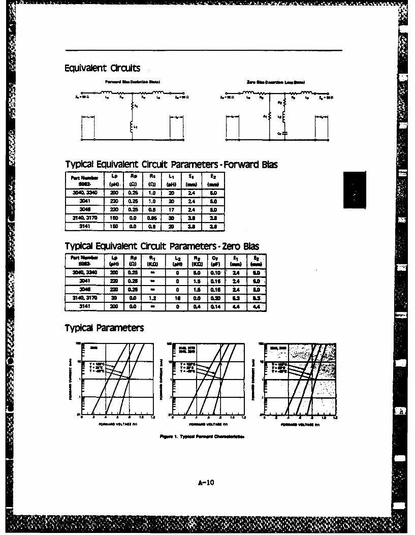
Equivalent CircuitsPwvmd WMullsMlmth SO"a 2w. an anmm L.Sw
-SonD I.o %g 5g Lo 70.Ufl zoon %% 4 60
E1 Fl ____
Typical Equivalent Circuit Parameters - Forwar BiaPut Numb Lp Rp Rs Ll 21 22
5062. Ip1). (fl) (IN (pH4) (mm (mm)
3040,3340 200 0.2 1.0 20 2.4 5.03041 220 0.25 1.0 20 2.4 5.
2140.370 150 0. 0MN 30 2.3 3.2141 150 0.0 0.8 w 3.3 3.
Typical Equivalent Circuit Parameter - Zero SIasuFwt NuAM Lp Np N1 L2
3R2 CT 94 fSmum (pH4) IMl WOD (PH4) (1W (PU) (mI 1m
304.3340 200 0.5M 0 5.0 0.10 U. 5.03D41 22D 0.25 * 0 1.5 0.15 2.4 5.03046 0.25 0 1.5 0.15 2. 5.
3140.3170 30 0.0 1.2 16 0. 0.L20 U. 5.3141 M0 0. n 0 0.4 0.14 4.4 4.4
Typca Parmeters
-T -v Iw I A.~
0 1.8 A i 1.2 a ..2 4 i . . I
gPaflw VOLYs IV M SSM "TASS mV S VU V
ROM 1. TV~is Pemud ChiaWOOlMOM
A- 10

.SO
T 2
~-IL -.6 -
a 1A- -14 1 4 i
2 5 10A M 4 8 4 a s m l o M m a l ow42 1 4 4 I .
a" cm a mw mu "a 3muPMn L. TVPhd Imiasm LAbe" Zw. p~ga TYPbNW -Pw qey Mlu. A T vSM eis PO A .,s
WI
ft-=U6 SAT" 3141A
a-vv,! trT
lam.
PLO two
COaI46N "
PWgus 7. NP PasbapW ud a~. M P Paskwal 61 Wh Oubu. p~m &. lub ld $"lft@ Asmy.
A-il
1 0 li
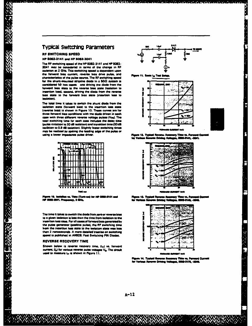
Typica Switchig Parameters m lm AT
HP 5062311adH M9301.3141 snd HP 502..04Tholtilswitching sPeed of the HP 56.14 n H 023041 mAY be considered in terms of the change in RIFisolation at 2 GHs. This switching spewt is dependent upon Tthe forward bias curent reverse bis drive pulse. and ~ * t s s.chawracerOMc Of the pulse source. The All switching speed O 1-no 11,Tosbfor the shunt-m'ounted str1illid in a 5011 syste is
bias stat to the forward bias stteinsertion loss to -
isolatioI.The total time it takes to switch the shunt diode fom the iisolation state 11forward bias) to the insertion les state
thr~m r bi coditonswith the diode divan in eachCO ihthree diffe re s otaeple (VpWm. Thex z ;f
total swvitch ing ti efo ach case includes tedelay time(pulse initiation to 20 do isolation) anid transition time(20d@ . ~ .
isolkmOn to 03dB iolaion) Slightiyfaste switching timee 'may be realised by spikin the loading ede of the Pulse or09using a lwrimpedance pulse driver. Fipm IL TWpl 111swem. AsssseuyIN*mvs. Ponws n s ea
ow Valis Aomus Doa Vellag UUo44 48$L
I pitiii~
1 '1
The time ittakes toswitc the diode fromsror reversebiasto a given Isolation is leoshan the time from isolation to the
the Pulse generator (positive puisel. the RP switch ing time I,from the insertion lose sate to the istion saewas lass ~-than 2 nanoseconds. A ore deteliod treatie en swtcingspeed is Published in AN92S; Fast Switching PIN Diodes.
REVERSE RECOVERY TIME. * . -.
Shown below is reverse recovery time. (tit) ve. forward , *curent 4l) for various revere Pulse voltages Vft. The cirouit U Uused to measure tp, is shown in Figure 11.meisa a
Figrs 14L Tyls Asin feAseary TMe vs, Peuvawd Currentfo yalsue Aseses r0 i Vellge UssnSlS 41M6
A-I12
Ahcuen Hybrid Couplers3 dB, 900Ultra-Miniature
Featuoe APPOIGelNOM
For installation directly in microstrip circuits Inexpensive power dividers and combinersLargest selection of frequency ranges and case styles Low cost balanced amplifier designsLowest cost Matrix amplifiersSmallest size, lightest weight Voltage variable PIN diode attenuatorsLaminated stripline construction Balanced mixers and modulatorsHigh isolation with low VSWR Switching networksRugged aluminum cases Balanced detectorsMeets MIL-E-5400 Class 3 requirements Antenna feed networks
Phase shifters and comparatorsDecripillon
This ultra-miniature series of 3 dB. 900 hybrid couplers is All Anaren ultra-miniature couplers are printed on stableavailable in 34 standard models and 15 case styles to teflon-glass substrates using shielded stripline techniques.cover the frequency range 30 MHz to 4.0 GHz. The popular They are laminated under hot ind pressure usin a low225-400 MHz band is covered by 4 standard case styles. loss dielectric bonding compound. The package asawes
high reliability and is capable of withstanding extremeAnaren ultra-miniature 3 dB, 900 hybrid couplers are well environmental stress.suited for a variety of applications: power dividers andcombiners, balanced amplifier circuits with low input and The couplers are designed to mate with 30 ml microstripoutput VSWR. matrix amplifiers, voltage variable PIN diode and mounting holes are provided for attaching the couplerattenuators, balanced mixers and modulators, switching ground plane. A reliable electrical ground contact isnetworks, balanced detectors, antenna teed networks and necessary for optimum performance.phase shifters and comparators.
The Anaren ultra-miniature coupler is a reciprocal four-po tThere are a number of techniques available for construct- network.ing microwave quadrature hybrids, but Anaren uses thebackward wave 3 dB. 900 hybrid coupler in striplino form. An input signal applied to any port (port 1. for example) willThis stripline version is smaller, provides better divide equally to the two opposite ports (3 and 4) with port 2Performance and can cover wider ban ihs than other remaining isolated. The voltage at port 4 lags the voltage attypes. The single-section, backward wave. 3 dB hybrid port 3 by 90. This phase quadrature relationship is in-allows octave bandwidth coverage and multi-section dependent of frequency and is the unique property whichversions can easily be designed to cover multi-octave and makes the 900 coupler so versatile.decade bandwidths.
See pages 45 and 71 for additional information.
A-13
I II l l g il 1 1 1 1 1 1 :_ ---II-

Electrtcail Specifications ____ ________
Model No. Frequency Isolation VSWR Insertion Anpltude Phae Case*(GHz) Min/Typ 'Max/Typ Loe Balance Blmnc Stle
______ (dfl) Max (d8) Max (din) (deI)10230-3 .030--076 15/20 1.40/1,20 0.35 ±0O.75 ±1.5 10210270-3 .030-.076 20/25 1.20/1.10 0.35 ±0.75 ±1.5 1031 A0270-3 .040--080 20/25 1.20/1.10 0.30 i0.50 ±1.5 1031 A0230-3 .054-.088 20/22 1.20/1.10 0.35 ±0.50 ±1.5 10210261 -3 .0625-125 20/27 1.20/1.10 0.35 ±0.50 ±1.5 1041 A0280-3 .090-.180 20/27 1.20/1.10 0.30 *0.50 ±1.5 1041 H0280-3 .090,180 18/25 1.20/1.10 0.30 ±0.50 ±1.5 116
180261-3 .100--200 20/25 1.20/1.10 0.30 *0.50 ±1.5 1041 J0280-3 .100,160 20/27 1.20/1.10 0.30 ±0.30 ±1.5 1161 A0920-3 .100--500 16/20 1.35/1.15 0.50 ±0.60 ±2.0 117A10280-3 .116-.150 20/27 1.20/1.10 0.30 ±0.30 ±11.5 10410262-3 -125-.250 20/27 1.20/1.10 0.30 ±0-50 ±1.5 10510260-3 .225-.400 20/25 1.20/1.10 0.30 *0.50 ±1.5 1061 A0260-3 .225-.400 20/25 1.2011.10 0.30 ±0.50 ±1.5 107I180260-3 .225-.400 20/25 1.20/1.10 0.30 ±0.50 ±1.5 108IR0260-3 .225-.400 20/25 1.20/1.10 0.30 ±0.50 ±1.5 1101S0260-3 .225-.400 20/25 1.20/1.10 0.30 ±0.50 ±1.5 106iMOz63-3 .250-500 20/22 1.20/1.10 0.30 ±0-50 ±1.5 11010263-3 .250-500 20/25 1.20/1.10 0.30 ±0.50 ±1.5 10610~0263-3 .300--550 20/25 1.20/1.10 0.30 ±0O.50 ±1.5 1061 A0263-3 .400-600 20/25 1.20/1.10 0.30 t0.50 ±1.5 10618B0263-3 .400-.700 20/25 1.20/1.10 0.30 ±0.50 ±1 .5 1081 H0264-3 .440-.880 20/25 1.20/1,10 0.30 ±0.50 ±11.5 111A10264-3 .500-1.0 20i25 1.20/1.10 0.30 ±0.50 ±1.5 ill1 B0264-3 .500-1.0 20/25 1.20/1.10 0.30 ±0.50 ±1.5 1121 A0264-3 .600-1.2 20/25 1.20/1.10 0.30 ±0.50 ±1.5 fill10330-3 .700-1.4 20/25 1.25/1.10 0.30 ±0.50 ±1.5 113
10890-3 .950-1.225 20/25 1.25/1.15 0.30 ±0.30 * ±1.5 11210265-3 1.0-2.0 20/24 1.25/1.10 0.30 ±0.50 ±11.5 11318B0265-3 1.0-2.0 20/24 1.25/1.15 0.30 ±0.50 ±1.5 1121 E0320-3 1.3-2.6 20/25 1.30/1.15 0.30 ±0.50 ±2.0 11310320-3 1.7-2.5 20/23 1.30/1.20 0.30 ±0.50 ±1.5 11318B0320-3 1.7-2.5 20/25 1.30/1.15 0.30 ±0.50 ±1.5 11210266-3 2.0-4.0 18/21 1.30/1 20 0.30 ±0.50 ±2.0 114
Power: 200 W @ 850C. Derate to 100 W @ 1000C. These specifcains apply for tests performed ith properlyDerate to Zero Wafts @ 1506C. designed rnicrostrip lest btixe.
Power rabn applies when solder tab/coupler Interface has Couplers meet environmental requkemerus of MIL-E-5400.been conformally coated to eklnae voltage breakdown. Ctass 3; as applicable.Nominal Impedance 50 ohms. non-reactive
A-1
Mpl''
z L

7N wN. ~-. 4 . -. N- -4 -
I-. - .- .~. 'I*MISSION''*
Row.. . . .. . .. . . .. . . . ZN Air'
tA
1*64-de to E"
P&4w
,I -' -" 1 414V1 1.-..
)Oft,4ltjloltmL~-% --
I .
* I~'~Z-'V
el A"NI~Na~vpw% ~ N 0, ff
, -4
g ;{~' '~~ '-N--