Embed Size (px)
Citation preview

Efficient Asynchronous Protocol Efficient Asynchronous Protocol Converters for Two-Phase Delay-Converters for Two-Phase Delay-
Insensitive Global CommunicationInsensitive Global Communication
Amitava MitraAmitava MitraIntel Corp., Bangalore, IndiaIntel Corp., Bangalore, India
William F. McLaughlinWilliam F. McLaughlinColumbia University, Electrical Columbia University, Electrical
EngineeringEngineering
Steven M. NowickSteven M. NowickColumbia University, Computer ScienceColumbia University, Computer Science

2
OutlineOutline Motivation and ContributionMotivation and Contribution
System-on-Chip: Concepts and TrendsSystem-on-Chip: Concepts and Trends Asynchronous Signaling StylesAsynchronous Signaling Styles Target Asynchronous SOC ArchitectureTarget Asynchronous SOC Architecture ContributionContribution
Proposed System ArchitectureProposed System Architecture
Experimental ResultsExperimental Results
Extensions: Other Signaling StylesExtensions: Other Signaling Styles
Conclusions and Future WorkConclusions and Future Work

3
System-on-Chip (SOC): Concept and System-on-Chip (SOC): Concept and TrendsTrends Microelectronic trends enabling SOC designMicroelectronic trends enabling SOC design
Increasing integration density + chip sizeIncreasing integration density + chip size Formerly discrete functions (memory, I/O) now integratedFormerly discrete functions (memory, I/O) now integrated Popularity of “multi-core” designs Popularity of “multi-core” designs
Heterogeneous SOC:Heterogeneous SOC: Large complex chip with broad functionalityLarge complex chip with broad functionality Many independent computation nodesMany independent computation nodes
Multiple cores, memories, accelerators, multimedia processing, Multiple cores, memories, accelerators, multimedia processing, etc. etc.
Often includes multiple timing domainsOften includes multiple timing domains Complex network-style interconnect fabricComplex network-style interconnect fabric
Challenges in Heterogeneous SOC design:Challenges in Heterogeneous SOC design: Wire costs not scaling down with device sizeWire costs not scaling down with device size
Increasing proportion of power and delay in interconnect Increasing proportion of power and delay in interconnect Robust and high-performance interconnect design:Robust and high-performance interconnect design:
High latencies between remote nodesHigh latencies between remote nodes Mixed timing, timing variability/uncertaintyMixed timing, timing variability/uncertainty Need to support varied components: modular/scalable designNeed to support varied components: modular/scalable design

4
SOC Communication FabricSOC Communication Fabric Growing factor in overall system performanceGrowing factor in overall system performance Ideal Requirements:Ideal Requirements:
Speed: high throughput, low latency Speed: high throughput, low latency Low powerLow power Robust to timing variations Robust to timing variations Flexibility: integrate modular IPs and upgradesFlexibility: integrate modular IPs and upgrades
Asynchronous design well-suited to these goalsAsynchronous design well-suited to these goals Timing robust flexible designsTiming robust flexible designs Lower power than synchronousLower power than synchronous Work by Quinton, Greenstreet, and Wilton [ICCD 2005]Work by Quinton, Greenstreet, and Wilton [ICCD 2005]
GALS-style: GALS-style: – global LEDR interconnect + local synchronous blocksglobal LEDR interconnect + local synchronous blocks– does not provide details of protocol convertersdoes not provide details of protocol converters

5
Asynchronous for SOC Asynchronous for SOC CommunicationCommunication Advantages of asynchronous global Advantages of asynchronous global
communicationcommunication Delay-insensitive (DI) encodingDelay-insensitive (DI) encoding
Removes timing constraints on global routing Removes timing constraints on global routing No clock signals to route across chipNo clock signals to route across chip
Significant power advantageSignificant power advantage Can support both async + sync computationCan support both async + sync computation
Delay-insensitive async logic combats growing variability Delay-insensitive async logic combats growing variability concernsconcerns
GALS style: Globally-Asynchronous Locally-SynchronousGALS style: Globally-Asynchronous Locally-Synchronous
Several popular async signaling protocolsSeveral popular async signaling protocols Dual rail four-phase, LEDR, 1-of-4, bundled data, Dual rail four-phase, LEDR, 1-of-4, bundled data,
othersothers No single protocol ideal for both logic and No single protocol ideal for both logic and
communicationcommunication

6
Background: LEDR SignalingBackground: LEDR Signaling Dual-rail encoding: two wires per bit – Dual-rail encoding: two wires per bit – delay-delay-
insensitiveinsensitive ““Level-encoding”:Level-encoding”:
Data rail: holds actual data valueData rail: holds actual data value Parity rail: holds parity valueParity rail: holds parity value
Alternating-phase protocol: Alternating-phase protocol: Encoding parity alternates between odd and even Encoding parity alternates between odd and even
00 11
EvenEven 0 0 00 1 1 11
OddOdd 0 0 11 1 1 00
LEDR LEDR EncodinEncodin
gg
Bit valueBit value
PhasePhase
data rail data rail parity railparity rail

7
LEDR SignalingLEDR Signaling
Exactly one wire transition for each new data itemExactly one wire transition for each new data item
datadata
parityparity
eveneven oddodd eveneven evenevenoddodd evenevenoddodd
Data rail: carries Data rail: carries bit value in both bit value in both
phasesphases
Parity rail: phase alternates Parity rail: phase alternates with each data itemwith each data item
00 11 00 00 11 11 11
8
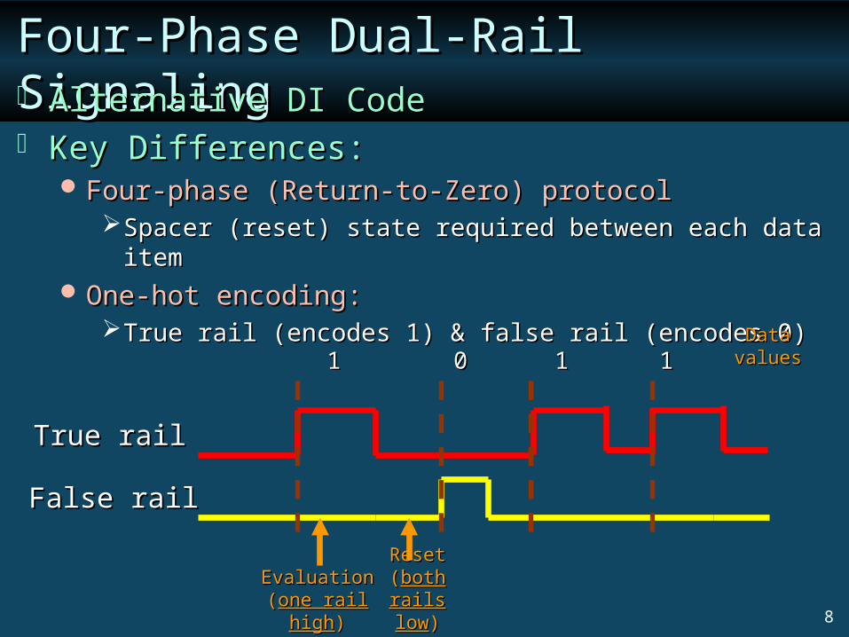
Four-Phase Dual-Rail SignalingFour-Phase Dual-Rail Signaling Alternative DI CodeAlternative DI Code Key Differences:Key Differences:
Four-phase (Return-to-Zero) protocolFour-phase (Return-to-Zero) protocolSpacer (reset) state required between each data itemSpacer (reset) state required between each data item
One-hot encoding: One-hot encoding: True rail (encodes 1) & false rail (encodes 0)True rail (encodes 1) & false rail (encodes 0)
True railTrue rail
False railFalse rail
Evaluation Evaluation ((one rail one rail
highhigh))
Reset Reset ((both rails both rails
lowlow))
11 00 11 11 Data valuesData values

9
Four-Phase Dual-Rail vs. LEDRFour-Phase Dual-Rail vs. LEDR Advantages of four-phase dual-rail: Advantages of four-phase dual-rail:
Delay-insensitive logic using standard gates Delay-insensitive logic using standard gates Implementations are simple and fast: widely usedImplementations are simple and fast: widely usedLEDR: complex & impractical LEDR: complex & impractical
Disadvantages of four-phase dual-rail:Disadvantages of four-phase dual-rail: System-level communication throughput: System-level communication throughput:
Spacer state doubles round-trip communication latencySpacer state doubles round-trip communication latencyLEDR: LEDR: no spacer requiredno spacer required
Power dissipation:Power dissipation:Two transitions/bit (up and down) for each data itemTwo transitions/bit (up and down) for each data itemLEDR: LEDR: only one transition/bitonly one transition/bit
Conclusion:Conclusion: Four-phase dual-rail better for implementing Four-phase dual-rail better for implementing function function
blocksblocks LEDR is better for LEDR is better for global communicationglobal communication

10
Target Asynchronous SOC Target Asynchronous SOC ArchitectureArchitecture
Three major components:Three major components: Global communication network (LEDR)Global communication network (LEDR) Local computation nodes (varied styles)Local computation nodes (varied styles) New requirement: New requirement: protocol convertersprotocol converters at interfaces at interfaces
Allow full separation of computation and communicationAllow full separation of computation and communication
Our goal –Our goal –Protocol converters Protocol converters
to enable this to enable this global LEDR SOCglobal LEDR SOC
4 phase data server
LEDR encode
LEDR decode 4 phase
function block
LEDR encode
LEDR decode
Cross-chip
LEDR channel
Pipeline stage,
arbitrary internal
signaling
LEDR decode
LEDR encode
Pipeline stage,
arbitrary internal
signaling
LEDR decode
LEDR encode
acknowledge
Cross-chip LEDR channel
11
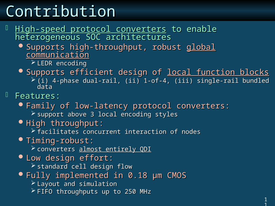
ContributionContribution High-speed protocol convertersHigh-speed protocol converters to enable to enable
heterogeneous SOC architecturesheterogeneous SOC architectures Supports high-throughput, robust Supports high-throughput, robust global global
communicationcommunication LEDR encodingLEDR encoding
Supports efficient design of Supports efficient design of local function blockslocal function blocks (i) 4-phase dual-rail, (ii) 1-of-4, (iii) single-rail bundled data(i) 4-phase dual-rail, (ii) 1-of-4, (iii) single-rail bundled data
Features:Features: Family of low-latency protocol converters: Family of low-latency protocol converters:
support above 3 local encoding stylessupport above 3 local encoding styles High throughput: High throughput:
facilitates concurrent interaction of nodesfacilitates concurrent interaction of nodes Timing-robust: Timing-robust:
converters converters almost entirely QDIalmost entirely QDI Low design effort:Low design effort:
standard cell design flow standard cell design flow Fully implemented in 0.18 Fully implemented in 0.18 μμm m CMOSCMOS
Layout and simulationLayout and simulation FIFO throughputs up to 250 MHz FIFO throughputs up to 250 MHz

12
Two Target SOC TopologiesTwo Target SOC Topologies
Pipeline stage,
arbitrary internal
signaling
LEDR decode
LEDR encode
Pipeline stage,
arbitrary internal
signaling
LEDR decode
LEDR encode
acknowledge
1. “Pipeline-style” topology1. “Pipeline-style” topology
Feed-forward data path: Feed-forward data path: uni-directionaluni-directional token flow token flow
Receiving node returns a single ACK (control signal)Receiving node returns a single ACK (control signal) Supports concurrency between nodesSupports concurrency between nodes
Data Data feeds feeds
forwardforward
Acknowledge Acknowledge sent backsent back

13
Two SOC Topologies (cont.)Two SOC Topologies (cont.)2. “Server-style” topology2. “Server-style” topology
Client passes data token to serverClient passes data token to server Server computes/returns data token to client (result)Server computes/returns data token to client (result)
Explicit ACK unnecessaryExplicit ACK unnecessary
Proposed SOC architecture supports both Proposed SOC architecture supports both topologiestopologies
4 phase data server
LEDR encode
LEDR decode 4 phase
function block
LEDR encode
LEDR decode
Bi-directionalBi-directional data flow: data data flow: data passed back to client on completionpassed back to client on completion
Four-phase Four-phase data clientdata client
Four-Four-phase phase serveserve
rr

14
OutlineOutline Motivation and ContributionMotivation and Contribution
Proposed System ArchitectureProposed System Architecture Architecture OverviewArchitecture Overview System SimulationSystem Simulation Detailed Hardware ImplementationDetailed Hardware Implementation Timing AnalysisTiming Analysis
Experimental ResultsExperimental Results
Extensions: Other Signaling StylesExtensions: Other Signaling Styles
Conclusions and Future WorkConclusions and Future Work
15
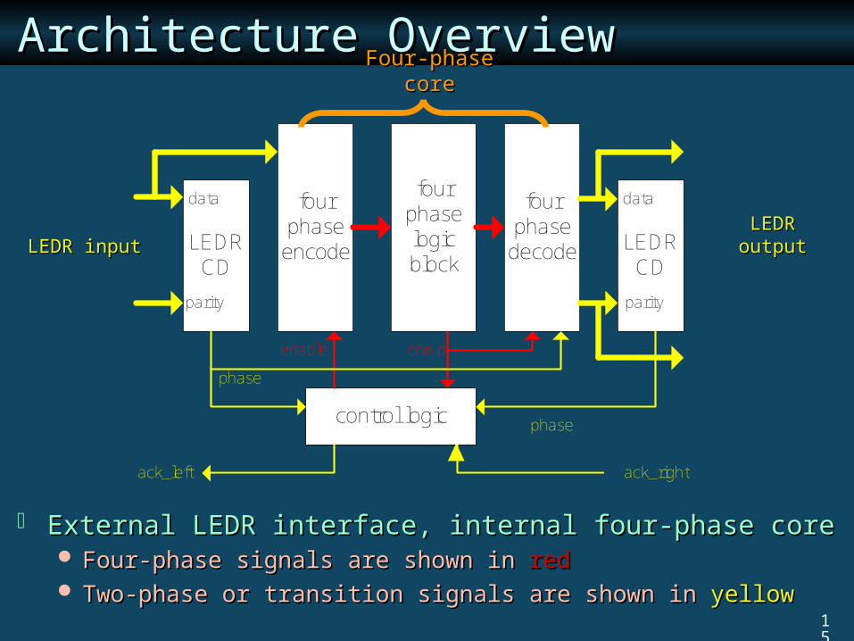
Architecture OverviewArchitecture Overview
External LEDR interface, internal four-phase coreExternal LEDR interface, internal four-phase core Four-phase signals are shown in Four-phase signals are shown in redred Two-phase or transition signals are shown in Two-phase or transition signals are shown in yellowyellow
LEDR CD
four phase
encode
four phase logic block
four phase
decode
control logic
data
parity
LEDR CD
data
parity
phase
phase
enable comp
ack_left ack_right
LEDR inputLEDR inputLEDR LEDR
outputoutput
Four-phase coreFour-phase core

16
Control SignalsControl Signals Two-phase Two-phase control signalscontrol signals
LEDR CD
four phase
encode
four phase logic block
four phase
decode
control logic
data
parity
LEDR CD
data
parity
phase
phase
enable comp
ack_left ack_right
Phase of Phase of LEDR LEDR input input
(request (request from left)from left)
Phase of Phase of LEDR output LEDR output
(forward (forward complete)complete)
AcknowledgAcknowledge to left e to left neighborneighbor
AcknowledgAcknowledge from right e from right
neighborneighbor

17
Control SignalsControl Signals Four-phase Four-phase control signalscontrol signals
LEDR CD
four phase
encode
four phase logic block
four phase
decode
control logic
data
parity
LEDR CD
data
parity
phase
phase
enable comp
ack_left ack_right
Enable four-Enable four-phase phase
evaluate and evaluate and RZRZ
Completion Completion detect four-detect four-
phase phase evaluate evaluate and RZand RZ

18
LEDR CD
four phase encode
four phase logic block
four phase
decode
control logic
data
parity
LEDR CD
data
parity
phase
phase
enable comp
ack_left ack_right
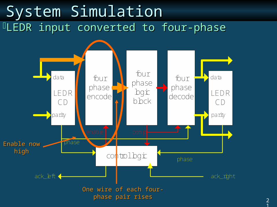
System SimulationSystem Simulation
Completion Completion detectiondetection
LEDR inputs begin arriving at quiescent systemLEDR inputs begin arriving at quiescent system
LEDR inputs LEDR inputs arrivearrive

19
System SimulationSystem Simulation
LEDR CD
four phase encode
four phase logic block
four phase
decode
control logic
data
parity
LEDR CD
data
parity
phase
phase
enable comp
ack_left ack_right
All input All input phases phases matchinmatchin
gg
Transition Transition to new to new phasephase
Input completion detection sent to controlInput completion detection sent to control

20
System SimulationSystem Simulation
LEDR CD
four phase encode
four phase logic block
four phase
decode
control logic
data
parity
LEDR CD
data
parity
phase
phase
enable comp
ack_left ack_right
Enable risesEnable rises
Control enables four-phase Control enables four-phase evaluateevaluate phase phase
21
System SimulationSystem Simulation
LEDR CD
four phase encode
four phase logic block
four phase
decode
control logic
data
parity
LEDR CD
data
parity
phase
phase
enable comp
ack_left ack_right
Enable now Enable now highhigh
LEDR input converted to four-phaseLEDR input converted to four-phase
One wire of each four-phase One wire of each four-phase pair risespair rises
22
LEDR CD
four phase encode
four phase logic block
four phase
decode
control logic
data
parity
LEDR CD
data
parity
phase
phase
enable comp
ack_left ack_right
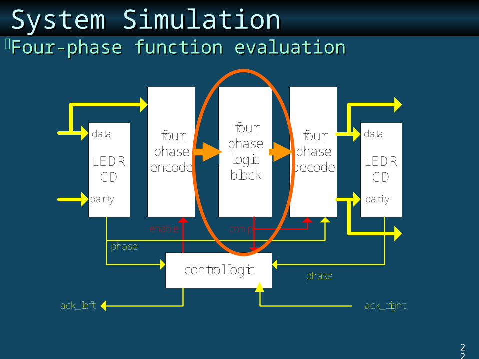
System SimulationSystem SimulationFour-phase function evaluationFour-phase function evaluation

23
LEDR CD
four phase encode
four phase logic block
four phase
decode
control logic
data
parity
LEDR CD
data
parity
phase
phase
enable comp
ack_left ack_right
System SimulationSystem SimulationFour-phase bits decoded to LEDRFour-phase bits decoded to LEDR
Each bit converted as soon as it computesEach bit converted as soon as it computes
Four-phase Four-phase complete not complete not
used in evaluate used in evaluate phasephase
LEDR LEDR outputs to outputs to next node next node generatedgenerated

24
LEDR CD
four phase
encode
four phase logic block
four phase
decode
control logic
data
parity
LEDR CD
data
parity
phase
phase
enable comp
ack_left ack_right
System SimulationSystem SimulationLEDR output completion detectionLEDR output completion detection
ACK from right ACK from right may come any may come any time after all time after all pairs are sentpairs are sent
Output Output pairspairs

25
LEDR CD
four phase
encode
four phase logic block
four phase
decode
control logic
data
parity
LEDR CD
data
parity
phase
phase
enable comp
ack_left ack_right
System SimulationSystem SimulationControl enables four-phase Control enables four-phase resetreset phase phase
Enable fallsEnable falls

26
LEDR CD
four phase encode
four phase logic block
four phase
decode
control logic
data
parity
LEDR CD
data
parity
phase
phase
enable comp
ack_left ack_right
System SimulationSystem Simulation
Enable now Enable now lowlow
Pipeline concurrencyPipeline concurrency: : request new data during reset request new data during reset
phasephase
Function block inputs return-to-zeroFunction block inputs return-to-zeroACK is sent concurrently to leftACK is sent concurrently to left

27
Reset Reset Completion Completion detectiondetection
System SimulationSystem Simulation
LEDR CD
four phase encode
four phase logic block
four phase
decode
control logic
data
parity
LEDR CD
data
parity
phase
phase
enable comp
ack_left ack_right
New data may New data may arrive now arrive now
that ACK has that ACK has been sentbeen sent
Enable remains Enable remains lowlow
Four-phase reset propagates through logic blockFour-phase reset propagates through logic block

28
System SimulationSystem Simulation
LEDR CD
four phase encode
four phase logic block
four phase
decode
control logic
data
parity
LEDR CD
data
parity
phase
phase
enable comp
ack_left ack_right
Four-phase reset completesFour-phase reset completesComplete internal cycle has now been performedComplete internal cycle has now been performed
Complete Complete fallsfalls

29
LEDR CD
four phase encode
four phase logic block
four phase
decode
control logic
data
parity
LEDR CD
data
parity
phase
phase
enable comp
ack_left ack_right
System SimulationSystem Simulation
Complete low Complete low (means reset (means reset
finished)finished)
New New evaluateevaluate phase begins when Enable rises phase begins when Enable rises againagain
Pre-conditions: reset finished, new data REQ, and old Pre-conditions: reset finished, new data REQ, and old data ACKdata ACK Three-way Three-way
synchronizationsynchronization
Input phase Input phase transitions when transitions when new data readynew data ready ACK transitions ACK transitions
when outputs when outputs safe to changesafe to change

30
Detailed Hardware Detailed Hardware ImplementationImplementation
Each block implemented in CMOS standard cellsEach block implemented in CMOS standard cells Design has few non-QDI timing constraintsDesign has few non-QDI timing constraints
LEDR CD
four phase
encode
four phase logic block
four phase
decode
control logic
data
parity
LEDR CD
data
parity
phase
phase
enable comp
ack_left ack_right
LEDR inputLEDR inputLEDR LEDR
outputoutput
Four-phase coreFour-phase core

31
Four-phase Encode (Input Four-phase Encode (Input Converter)Converter) Converts LEDR input to four-phase dual-railConverts LEDR input to four-phase dual-rail
Enable=‘1’: outputs evaluate based on LEDR dataEnable=‘1’: outputs evaluate based on LEDR dataEnable=‘0’: outputs reset (Enable=‘0’: outputs reset (LEDR data blockedLEDR data blocked))
Enable
LEDR data bit
Four-phase true rail
Four-phase false rail
LEDR CD
four phase encode
four phase logic block
four phase decode
control logic
data
parity
LEDR CD
data
parity
phase
phase
enable comp
ack_left ack_right

32
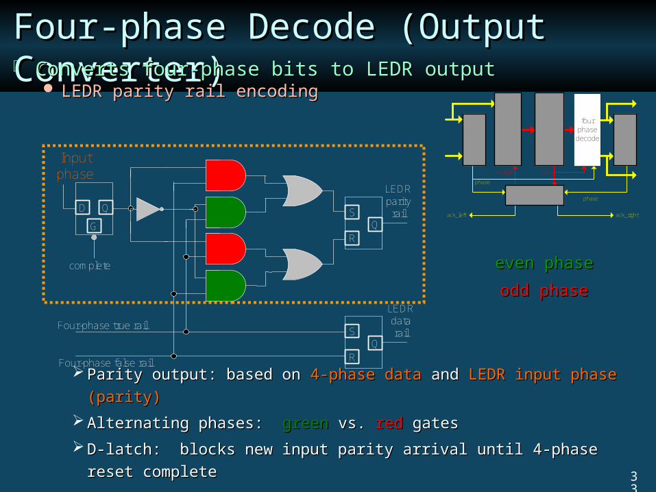
Four-phase Decode (Output Four-phase Decode (Output Converter)Converter) Converts four-phase bits to LEDR outputConverts four-phase bits to LEDR output
LEDR data rail encodingLEDR data rail encoding
Assert either S (1 value) or R (0 value), then return-to-holdAssert either S (1 value) or R (0 value), then return-to-hold
More robust alternative: C-elementMore robust alternative: C-element
D Q
GS
RQ
S
RQ
Input phase
complete
Four-phase true rail
Four-phase false rail
LEDRparity
rail
LEDRdata rail
LEDR CD
four phase encode
four phase logic block
four phase decode
control logic
data
parity
LEDR CD
data
parity
phase
phase
enable comp
ack_left ack_right
33
Four-phase Decode (Output Four-phase Decode (Output Converter)Converter) Converts four-phase bits to LEDR outputConverts four-phase bits to LEDR output
LEDR parity rail encodingLEDR parity rail encoding
Parity output: based on Parity output: based on 4-phase data4-phase data and and LEDR input phase (parity)LEDR input phase (parity)
Alternating phases: Alternating phases: greengreen vs. vs. redred gates gates
D-latch: blocks new input parity arrival until 4-phase reset D-latch: blocks new input parity arrival until 4-phase reset
completecomplete
D Q
GS
RQ
S
RQ
Input phase
complete
Four-phase true rail
Four-phase false rail
LEDRparity
rail
LEDRdata rail
LEDR CD
four phase encode
four phase logic block
four phase decode
control logic
data
parity
LEDR CD
data
parity
phase
phase
enable comp
ack_left ack_right
even phaseeven phase
odd phaseodd phase
34
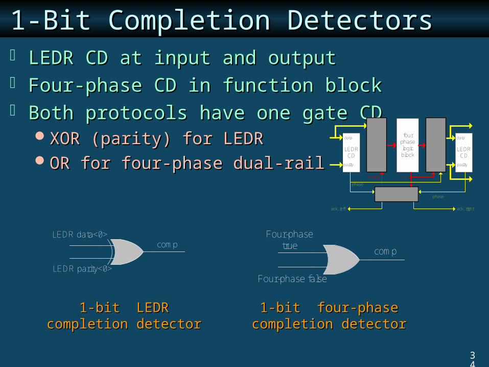
1-Bit Completion Detectors1-Bit Completion Detectors LEDR CD at input and outputLEDR CD at input and output Four-phase CD in function blockFour-phase CD in function block Both protocols have one gate CDBoth protocols have one gate CD
XOR (parity) for LEDRXOR (parity) for LEDROR for four-phase dual-railOR for four-phase dual-rail
LEDR data<0>
LEDR parity<0>
compFour-phase
true
Four-phase false
comp
LEDR CD
four phase encode
four phase logic block
four phase decode
control logic
data
parity
LEDR CD
data
parity
phase
phase
enable comp
ack_left ack_right
1-bit LEDR completion 1-bit LEDR completion detectordetector
1-bit four-phase 1-bit four-phase completion detectorcompletion detector

35
N-Bit Completion Detectors N-Bit Completion Detectors C-element treesC-element trees
Used for both LEDR and four-phaseUsed for both LEDR and four-phase
C-element: standard cell implementation (AOI222 C-element: standard cell implementation (AOI222
w/feedback)w/feedback)
C
C
C
LEDR data<0>
LEDR parity<0>
LEDR parity<1>
LEDR data<1>
LEDR parity<N-1>
LEDR data<N-1>
phase
BY
A
LEDR CD
four phase encode
four phase logic block
four phase decode
control logic
data
parity
LEDR CD
data
parity
phase
phase
enable comp
ack_left ack_right
36
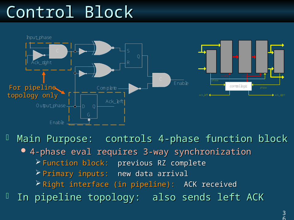
Control Block Control Block
Main Purpose: controls 4-phase function blockMain Purpose: controls 4-phase function block 4-phase eval requires 3-way synchronization4-phase eval requires 3-way synchronization
Function block:Function block: previous RZ complete previous RZ complete Primary inputs:Primary inputs: new data arrival new data arrival Right interface (in pipeline):Right interface (in pipeline): ACK received ACK received
In pipeline topology: also sends left ACK In pipeline topology: also sends left ACK
S
RQ
D Q
G
EnableC
C
Input_phase
Ack_right
Output_phaseAck_left
Complete
Enable
LEDR CD
four phase encode
four phase logic block
four phase decode
control logic
data
parity
LEDR CD
data
parity
phase
phase
enable comp
ack_left ack_right
For pipeline For pipeline topology onlytopology only

37
Control Block Control Block Converts Converts two-phasetwo-phase inputs to inputs to four-phasefour-phase
outputsoutputs
S
RQ
D Q
G
EnableC
C
Input_phase
Ack_right
Output_phase Ack_left
Complete
Enable
Two-phase to Two-phase to four-phase four-phase conversionconversion
38
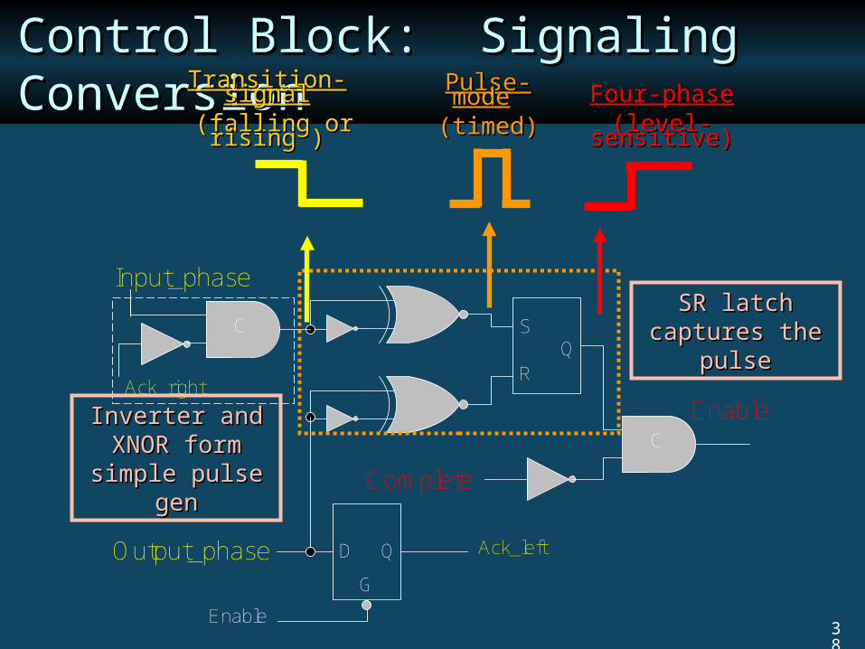
Control Block: Signaling Control Block: Signaling ConversionConversion
S
RQ
D Q
G
EnableC
C
Input_phase
Ack_right
Output_phase Ack_left
Complete
Enable
Transition-signalTransition-signal (falling or rising )(falling or rising )
Pulse-Pulse-modemode (timed)(timed)
Four-phaseFour-phase(level-(level-
sensitive)sensitive)
Inverter and Inverter and XNOR form XNOR form
simple pulse simple pulse gengen
SR latch SR latch captures the captures the
pulsepulse
39
Timing RequirementsTiming Requirements Circuits Circuits almost entirelyalmost entirely QDI QDI Exceptions:Exceptions:
Control block:Control block:Two-sided timing constraint on length of pulseTwo-sided timing constraint on length of pulseSensitive to both gate and wire delaysSensitive to both gate and wire delaysCareful layout requiredCareful layout required
Latches: simple hold time constraints Latches: simple hold time constraints SR latches can be replaced by C-elementsSR latches can be replaced by C-elements
– C-elements also have implementation-specific timing C-elements also have implementation-specific timing constraintsconstraints
– SR latch much faster than our standard cell C-elementSR latch much faster than our standard cell C-elementD latch can be removed at cost of concurrencyD latch can be removed at cost of concurrency

40
OutlineOutline Motivation and ContributionMotivation and Contribution
Proposed System ArchitectureProposed System Architecture
Experimental ResultsExperimental Results Design MethodologyDesign Methodology Datapath SetupDatapath Setup Simulation Results Simulation Results Latency and Throughput AnalysisLatency and Throughput Analysis
Extensions: Other Signaling StylesExtensions: Other Signaling Styles
Conclusions and Future WorkConclusions and Future Work

41
Design Methodology Design Methodology Standard cell design flow with complete layoutStandard cell design flow with complete layout
0.18 0.18 μμm TSMC CMOS processm TSMC CMOS process 4 metal layers of 7 available used in routing4 metal layers of 7 available used in routing
Custom place-and-route usedCustom place-and-route used Only major layout concern: pulse generator circuitOnly major layout concern: pulse generator circuit Design could be automated with constraints on pulseDesign could be automated with constraints on pulse
Analog simulations: based on layout-extracted Analog simulations: based on layout-extracted designdesign Test vectors including limiting fast and slow casesTest vectors including limiting fast and slow cases

42
Datapath Implementation Datapath Implementation Two function blocks implementedTwo function blocks implemented
An 8x8 carry-save multiplierAn 8x8 carry-save multiplier An empty FIFO stageAn empty FIFO stage
FIFO contains four-phase completion detector onlyFIFO contains four-phase completion detector onlyDemonstrates minimum possible node latencyDemonstrates minimum possible node latency
Blocks are QDI in evaluate, but “eager” in Blocks are QDI in evaluate, but “eager” in resetreset Implemented in combinational CMOSImplemented in combinational CMOS ““DIMS”-style logic (with C-elements) could be used DIMS”-style logic (with C-elements) could be used
insteadinsteadQDI in both directionsQDI in both directions Increases both forward and reverse latenciesIncreases both forward and reverse latencies

43
Multiplier Layout Multiplier Layout
Includes dual rail multiplier and all conversion Includes dual rail multiplier and all conversion
circuitscircuitsTotal area of 0.051 mmTotal area of 0.051 mm22
FIFO stage has area of 0.018 mmFIFO stage has area of 0.018 mm22

44
Measured Block Latencies Measured Block Latencies
CategoryCategory Design BlockDesign Block Simulated Simulated LatencyLatency
Function block Function block latencies latencies (includes four-(includes four-phase phase completion completion detection)detection)
Multiplier evaluateMultiplier evaluate 4.2 – 4.9 ns4.2 – 4.9 ns
Multiplier resetMultiplier reset 2.2 ns2.2 ns
FIFO (evaluate or FIFO (evaluate or reset)reset)
0.7 ns0.7 ns
CD latencyCD latency LEDR completion LEDR completion detectordetector
1.3 ns1.3 ns (even) (even)
0.9 ns0.9 ns (odd) (odd)
Overhead of Overhead of convertersconverters
Input ConverterInput Converter 0.2 ns0.2 ns
Output ConverterOutput Converter 0.5 ns0.5 ns
Control block (longest Control block (longest path)path)
1.1 ns1.1 ns

45
Performance ResultsPerformance Results3 Metrics:3 Metrics: Forward Latency: Forward Latency:
input arrival input arrival output data available output data available Average Values: Multiplier:Average Values: Multiplier: 6.8 ns6.8 ns; FIFO:; FIFO: 2.9 ns2.9 ns..
Stabilization Time: Stabilization Time: input arrival input arrival reset complete (circuit reset complete (circuit
quiescent)quiescent) Multiplier:Multiplier: 10.5 ns10.5 ns; FIFO:; FIFO: 6.3 ns6.3 ns..
Pipelined Cycle Time: Pipelined Cycle Time: min processing time/data item (steady-min processing time/data item (steady-
state)state) Multiplier:Multiplier: 8.3 ns8.3 ns; FIFO; FIFO 4.0 ns4.0 ns..

46
Performance Analysis Performance Analysis Forward latency: overheadForward latency: overhead
2.2 ns2.2 ns for both nodes for both nodes Overhead independent of function block sizeOverhead independent of function block size
Includes:Includes: LEDR CD, control unit, input/output convertersLEDR CD, control unit, input/output converters
Throughput: increased by concurrencyThroughput: increased by concurrency Benefit: Benefit: 2.2 ns2.2 ns reduction in cycle time (vs. post-reset ACK) reduction in cycle time (vs. post-reset ACK) Savings achieved even in environment Savings achieved even in environment withoutwithout channel channel
latencylatency ““Core converter” overhead (no CD) extremely lowCore converter” overhead (no CD) extremely low
Only Only 1.1 ns 1.1 ns average latency for converters + controlaverage latency for converters + control Completion detectors: Completion detectors:
Account for half of forward latency overheadAccount for half of forward latency overhead Account for 55% of FIFO cycle timeAccount for 55% of FIFO cycle time
Faster CDs would provide big improvementFaster CDs would provide big improvement

47
OutlineOutline Motivation and ContributionMotivation and Contribution
Proposed System ArchitectureProposed System Architecture
Experimental ResultsExperimental Results
Extensions: Other Signaling StylesExtensions: Other Signaling Styles Converters for 1-of-4 function blocksConverters for 1-of-4 function blocks Converters for bundled data function blockConverters for bundled data function block
Conclusions and Future WorkConclusions and Future Work

48
Extensions to Other Local Extensions to Other Local Protocols Protocols Only small changesOnly small changes to handle to handle 1-of-41-of-4 or or
bundled data bundled data No change to control blockNo change to control block
1-of-4 encoding:1-of-4 encoding: Input/output converters:Input/output converters:
Small changes to logicSmall changes to logic Needs standard 1-of-4 completion detectorNeeds standard 1-of-4 completion detector
Single-rail bundled dataSingle-rail bundled data:: Input converter: not needed – use LEDR data railInput converter: not needed – use LEDR data rail Output converter:Output converter:
New basic circuit required New basic circuit required (see paper for details)(see paper for details) Function block completion detection:Function block completion detection:
Use bundled ‘done’ signalUse bundled ‘done’ signalAsymmetric delay chain (fast reset)Asymmetric delay chain (fast reset)

49
OutlineOutline Background and MotivationBackground and Motivation
ContributionContribution
Proposed System ArchitectureProposed System Architecture
Experimental ResultsExperimental Results
Extensions: Other Signaling StylesExtensions: Other Signaling Styles
Conclusions and Future WorkConclusions and Future Work Summary and ConclusionSummary and Conclusion Future WorkFuture Work

50
Summary and Conclusions Summary and Conclusions Support heterogeneous SOCs using Support heterogeneous SOCs using hybrid hybrid
protocolsprotocols LEDR: low-power, delay-insensitive LEDR: low-power, delay-insensitive communication fabriccommunication fabric Dual rail four-phase: Simple, fast Dual rail four-phase: Simple, fast logic blockslogic blocks
Designed Converters for LEDR/four-phase SOC:Designed Converters for LEDR/four-phase SOC: Low latency, high throughput, timing robust designLow latency, high throughput, timing robust design
Robust concurrency system developedRobust concurrency system developed Exploits four-phase reset to mask communication timeExploits four-phase reset to mask communication time
Simulations with realistic mid-sized function Simulations with realistic mid-sized function nodesnodes Demonstrated low latency overheadDemonstrated low latency overhead Demonstrated low area overheadDemonstrated low area overhead Achieved throughputs up to 250 MHz for FIFO stageAchieved throughputs up to 250 MHz for FIFO stage

51
Future Work Future Work Evaluating system-level benefitsEvaluating system-level benefits
Determine design spaces where converters most Determine design spaces where converters most usefulusefulQuantify benefits over using either protocol exclusivelyQuantify benefits over using either protocol exclusively
Optimal partitioning of converter nodesOptimal partitioning of converter nodes Explore dependence on system topology Explore dependence on system topology
Potential applications: use in async SOCsPotential applications: use in async SOCs Beigne/Vivet – GALS NoC Architectures (Async-06)Beigne/Vivet – GALS NoC Architectures (Async-06) Scott et al. (Intel/Silistix) – PXA27x System (Async-07)Scott et al. (Intel/Silistix) – PXA27x System (Async-07) Dobkin/Ginosar/Kolodny – fast LEDR serial links (Async-Dobkin/Ginosar/Kolodny – fast LEDR serial links (Async-
06/07)06/07)Convert 4-phase dual-rail to LEDR (for parallel load)Convert 4-phase dual-rail to LEDR (for parallel load)