Embed Size (px)
Citation preview

Effects of Quantization on Digital Buck
Converter Switch Mode Power Supply
Mark Lorenze Torregoza1 and Elmer R. Magsino
2
Electronics and Communications Engineering Department, Gokongwei College of Engineering,
De La Salle University-Manila, Taft Avenue, Philippines
Email: [email protected], [email protected]
Jessica C. Cabiles-Magsino Electrical and Electronics Engineering Institute, University of the Philippines–Diliman, Philippines
Abstract—The development of power supplies has evolved
from using linear or series regulator to switch mode power
supplies (SMPS). Nowadays, SMPS have employed the use
of digital controllers such as microcontrollers and digital
signal processors (DSP’s) to provide compensation,
housekeeping, fan control, communication, etc. The main
advantages of using a digital controller are: insensitivity to
environment and component tolerances, repeatability,
predictability, flexibility and size reduction of power supply
units (PSUs). These are very much appealing to the
designer’s viewpoint; however, these come with
disadvantages such as limitation in bandwidth due to
sampling rate, peripheral’s speed and high prototyping cost.
In this paper, we observe one of the existing problems
revolving around the use of digital controllers in SMPS, i.e.
quantization.
Index Terms—quantization effects, buck converter, digital
signal processors
I. INTRODUCTION
The power supply industry is one of the fastest
growing industries in the world. In particular, switch
mode power supplies find its application in nearly all
consumer market such as communications, computers,
instrumentation and industrial control.
Power supplies employ different techniques in their
control methodology. Voltage mode control and current
mode control are the popular methods of controlling
power supplies. Principle of operation, as well as the
advantages and disadvantages of using either one of the
control methods have been discussed in [1]. With the
advantage of the current mode control over the voltage
mode control with regard to the dynamic response, it is
the more widely used practice in the industry. Applications of digital signal controllers in power
supplies have now become widespread. [2] They are used
in VRM’s, power factor correction circuits, inverters and
dc-dc converters. The benefits of using digital signal
controllers have been the subject of most research and
Manuscript received June 29, 2013; revised July 5, 2013
industry studies. [3] [4] [5] Advantages of using digital
control for power supplies include higher room for
efficiency optimization as the operation could be fully
maximized for the desired efficiency, programmability of
the device, thereby reducing the parts count, adaptive
power management, reduced sensitivity to temperature
and process variations and advanced control techniques.
Although the control method is digital, the converter’s
power stage is mostly analog. Therefore there exist
several issues when implementing the digital control for
the power converters. [6] One of these problems is the
effects of quantization.
Due to the fixed-point core of the DSC’s used in power
supply designs, limitations due to its nature of number
representation is also a concern during the design and
conceptualization stage. This study is undertaken to see
the quantization effects in a switched-mode power supply
particularly on these stages: (1) error voltage, (2)
compensation networks and (3) pulse width modulator. It
is also desired that the effects at each stage in
combination with the other stages be studied and quantify
the contribution of each to the overall system.
II. RELATED LITERATURE
Digital control loop defines a finite set of discrete “set
points” resulting from the resolution of the quantizing
elements in the system. The resolution of each block is
given by:
12
minmax
nR
VVV (1)
where VR is the resolution (in volts/step), Vmax/min is the
maximum/minimum input voltage of the block and n is
the number of bits of the quantizer. The smaller this value
is, the better. Quantization is applied on the following
stages of the power supply, namely: (1) error voltage, (2)
compensation network(s) and (3) pulse width modulator
(PWM). [7]
In a digitally-controlled power supply, the first step is
sampling the error voltage (reference voltage minus the
sampled output voltage) and converting it to its digital
154
Journal of Automation and Control Engineering Vol. 2, No. 2, June 2014
doi: 10.12720/joace.2.2.154-159©2014 Engineering and Technology Publishing

value. Ideally, the desired error voltage is zero but this
would always have a small value and must be well-
represented after quantization. The output voltage is
sampled by a zero order hold circuit with a sampling
frequency equal to twice the switching frequency of 100
kHz.
The block diagram of a digitally controlled SMPS is
shown in Fig. 1. Once the error voltage is quantized, it is
then passed to the compensation network. The
compensation network compares the output voltage to a
reference value and properly adjusts the pulse width to
provide voltage regulation. In digital control, phase shifts
are added due to the time delays in processing the data.
Figure 1. Block diagram of quantization scheme
The output of PWM, once quantized, becomes the
Digital Pulse Width Modulator, DPWM. DPWM
produces a discrete and finite set of duty ratio values, thus,
from a steady-state output, only a set of discrete output
voltages is possible.
It is in this sense that the resolution of the error voltage,
compensation network(s) and DPWM be high enough to
avoid a phenomenon known as limit-cycle oscillation and
mimic the analog response. [8]
III. METHODOLOGY
This research work uses MATLAB/Simulink and some
of its toolboxes to perform simulation of the performance
of a digitally controlled buck converter. The desired
system specifications for the simulation of a buck
regulator are given in Table I.
TABLE I. BUCK CONVERTER SPECIFICATIONS
Input Voltage (Vin) 20VDC
Output Voltage (Vout) 12VDC
Max Current Output (Iout) 2.5A
Current Ripple (Iripple) 0.1*Iout A
Voltage Ripple (Vreg) 0.01*Vout V
Phase Margin >45deg
Gain Margin >6dB
Regulation will be done using current-mode control
(CMC) as shown in Fig. 2. The current loop (Ti) is
derived from the model of the switching regulator,
modulator (PWM), the feedback transfer function and Ri,
which is a current to voltage conversion gain. On the
other hand, the voltage loop (Tv) comes from closing the
current loop and adding the compensation network. This
is the voltage-mode control (VMC) part.
Quantization is inserted on the following blocks: (1)
after getting the error voltage between VREF and VO, (2)
inside the compensation FC(s) and H(s) and (3) the
modulator FM. Since digital control heavily relies on its
counterpart, the analog control derivations are omitted.
Type II compensators will be used to achieve the desired
system specifications for the buck converter. It is to be
noted that the zero-pole placement of each compensator
is such that the zero and pole will cancel the effect of the
poles and zero of the buck open loop transfer function
and that the system achieves high gain at DC and lower
frequencies. [10]
Figure 2. Current mode control implementation
IV. RESULTS AND DISCUSSION
The results and analysis of a buck converter simulation
are given below.
A. Analog Control
The values of the inductor, capacitor and parasitic
values for the buck regulator are computed to achieve the
desired system specifications shown on Table I. The
values are: L=49.08uH, ESR=0.04Ω, C=153.4uF,
ESR=0.03Ω and D=0.61.
These values are now inserted into the “Buck
Converter” block, highlighted by a red circle in Fig. 3
while the static and dynamic responses of the closed loop
system are shown in Fig. 4.
The VMC and CMC compensators are achieved using
MATLAB’s Control System Toolbox SISO Design Tool
with stability margins: (for current-mode) GM = 6.3 dB
at 14k rad/sec and PM = 48.1 deg at 11.5k rad/sec and
(for voltage-mode) GM and PM are 6.02dB at 12.2k
rad/sec and 58.3 degrees at 1.76k rad/sec respectively.
The analog compensator for both the VMC and the
CMC is then converted into discrete-time with the use of
Tustin’s method shown in Table II.
TABLE II. ANALOG AND DIGITAL COMPENSATORS FOR THE BUCK
CONVERTER
155
Journal of Automation and Control Engineering Vol. 2, No. 2, June 2014
TABLE II. ANALOG AND DIGITAL COMPENSATORS FOR THE BUCK
CONVERTER
Analog Transfer Function Digital Transfer Function
2
2
0.312 0.0066 0.3054( )
1.872 0.872
z zH z vmc
z z
2
2
0.0037 0.003 0.0034( )
1.429 0.429
z zF z vmc
z z
©2014 Engineering and Technology Publishing

B. Digital Control
Under this section, the effects of quantization on each
part will be shown and discussed.
Figure 3. Closed loop buck converter system
(a)
(b)
Figure 4. Buck converter closed loop output waveforms (a) Static response and (b) Dynamic response (half to full load)
The digital control power supply is modelled in Fig. 5.
It shows the top-level closed loop digital model with the
digitized blocks denoted by the red dotted box. The first
highlighted block connected to the output voltage
emulates the Analog-to-Digital converter (ADC), the
voltage mode compensator and the current mode
compensator. On the other hand, the second highlighted
block connected to the output of the CMC and to the
input of the PWM converter emulates the Digital Pulse
Width Modulator. It is from these two blocks from which
the effects of quantization are observed.
Using a signed bit representation scheme, the number
of bits that is used to mimic the bits in the digital signal
controller is N. This is the main variable in the study and
its corresponding effect is observed. The bits
representation is limited to four, eight, twelve and sixteen
bits. To ensure that the quantization effect is prominent in
a particular block under observation, the remaining
blocks are quantized using a 32-bit representation.
Figure 5. Buck converter digital closed loop Top-Level model
The ADC block is composed of the following
subsystem, namely, the Zero Order Hold (ZOH), the
quantizer block and the saturation block. The quantizer
block is where the number of bits is changed.
The 4-bit representation of the quantizer yields an
output that is in the range of 12.18V to 12.205V.
Although it meets the output voltage of 12 V, it is outside
the regulation of the specified converter which allows ±
1% ripple.
Although, the number of bits used to represent the
ADC gives out the desired output voltage, the problem
that is seen in the 4-bit representation is in the resolution
of the quantizer. The smaller the resolution of the DSP,
the finer the step interval between the signal levels is
present.
An algorithm to demonstrate the quantization in an
IIR filter is developed. Equation 2 below was used to
derive the quantized coefficients of the original
coefficients [11]. The original coefficients are divided by
two to ensure that there are no coefficients greater than
one, and then multiplied by 2n. The floor value is taken
before dividing by 2n.
2
22n
ntcoefficienfloor
qCoeff
(2)
With the sampled error voltage having variations
particularly during loading and transient conditions, the
reference voltage seen at the point of the current mode
control must yield an almost constant value. A voltage
mode compensator, H(z) is used to control the said
variation. However, said compensator can be realized as
an IIR filter that has a finite representation. The
156
Journal of Automation and Control Engineering Vol. 2, No. 2, June 2014
©2014 Engineering and Technology Publishing

coefficients of the said compensator (filter) experiences
quantization errors as well. The unquantized transfer
function of the compensator for the voltage mode control
is given by
(3)
Using a 4-bit signed representation, the corresponding
transfer function becomes
(4)
The output voltage became 8.66V as seen from Figure
11. Computing the percent error, it can be seen that the %
error is:
(5)
An error of 27.8% is unacceptable in any power
supply.
Investigating further, from Fig. 6, it can be seen from
the plot of the duty cycle command that the duty is
roughly around 0.45%. For a buck converter, the input to
output relationship is given by: Vout = Duty*Vin =
0.45*20V = 8.5V.
It can be then said that the number of bits needed to
represent the compensator is higher than that of 4-bits.
Representing it at a lower bit will result in loss of
information.
Figure 6. Duty cycle command
At a higher bit representation, say N = 10, the desired
response was achieved.
The second control network is located at the current
mode control block. It is here where the sampled inductor
current is compared with the output of the voltage mode
control and any variation between the two has to be
compensated by the current mode controller, Fc(z).
As in the VMC compensator, the CMC compensator
can be thought of as an IIR filter with a finite
representation. The unquantized transfer function of the
current mode compensator as converted through bilinear
transformation is given by:
(6)
With a finite representation of a 4-bit signed integer,
the transfer function undergoes quantization with the
resulting equation as:
(7)
Notice that there are no visible zeros in the resulting
quantization. The same case happened even for increased
bits of 6, 8 and 10.
For a 12-bit representation, the power supply almost
approximates the response of the unquantized
compensator. The output voltage for the 12-bit
representation is shown below in Fig. 7.
Figure 7. Output voltage at CMC compensator, N=12
The inductor current undergoes the same process of
sampling and conversion to its digital equivalent. During
this conversion process, quantization also plays a
significant role in the performance of the power supply.
The error voltage between the VMC reference voltage
and the sampled inductor current is being controlled by
the current mode compensator. For a 4-bit representation,
the output voltage equals the specified value of 12.03 V.
Oscillations is present at the output and these oscillations
represent the limit cycle effect.
The digital pulse width modulator’s function is to
control the switching times of the switch network. Its
output is the duty cycle at which the converter would
operate. In its digital implementation, the number of bits
used to represent the PWM poses a limit to the value of
the duty cycle output.
In the case where the number of bits representation is
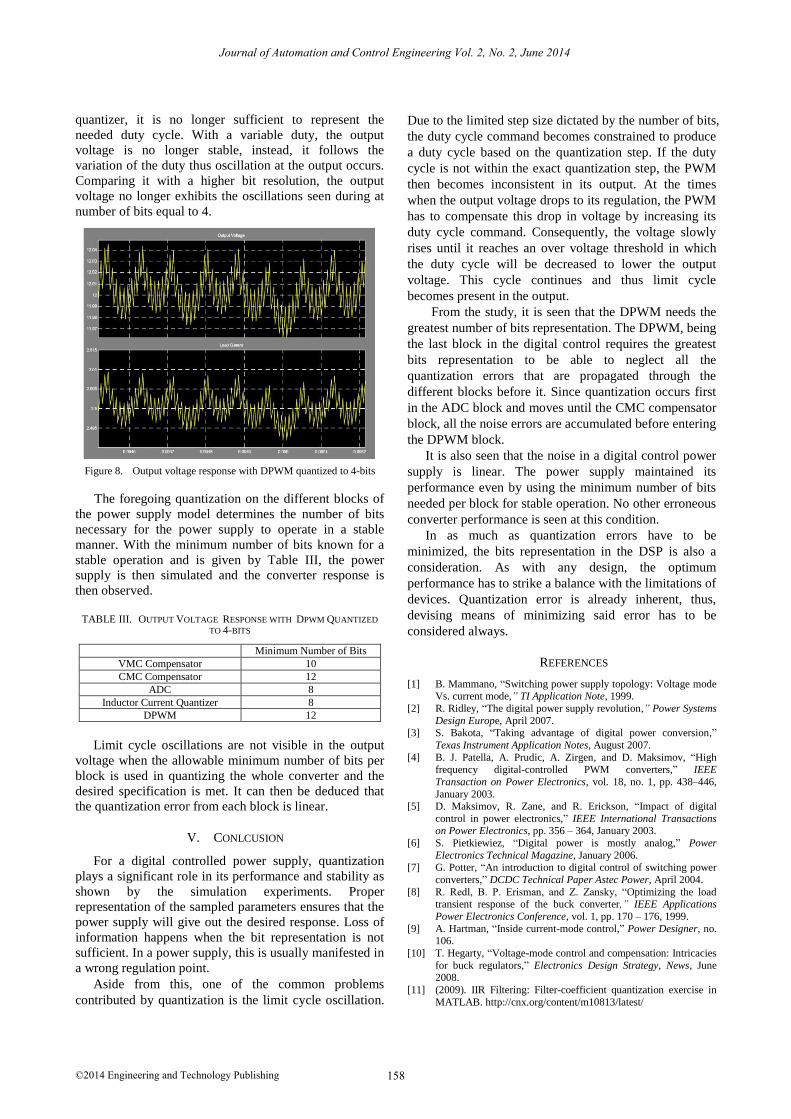
equal to 4, oscillations at the output are visible. The
voltage range of the output varies from 11.98V to 12.04V.
(Fig. 8)
Inspecting closely the output of the duty cycle
command block shows that the duty cycle command is
swinging from the range of 0.5 to 0.63.
The oscillations are attributed to the wide swing of the
duty cycle command. Due to the low resolution of the
157
Journal of Automation and Control Engineering Vol. 2, No. 2, June 2014
©2014 Engineering and Technology Publishing
158
Journal of Automation and Control Engineering Vol. 2, No. 2, June 2014
quantizer, it is no longer sufficient to represent the
needed duty cycle. With a variable duty, the output
voltage is no longer stable, instead, it follows the
variation of the duty thus oscillation at the output occurs.
Comparing it with a higher bit resolution, the output
voltage no longer exhibits the oscillations seen during at
number of bits equal to 4.
Figure 8. Output voltage response with DPWM quantized to 4-bits
The foregoing quantization on the different blocks of
the power supply model determines the number of bits
necessary for the power supply to operate in a stable
manner. With the minimum number of bits known for a
stable operation and is given by Table III, the power
supply is then simulated and the converter response is
then observed.
TABLE III. OUTPUT VOLTAGE RESPONSE WITH DPWM QUANTIZED
TO 4-BITS
Minimum Number of Bits
VMC Compensator 10
CMC Compensator 12
ADC 8
Inductor Current Quantizer 8
DPWM 12
Limit cycle oscillations are not visible in the output
voltage when the allowable minimum number of bits per
block is used in quantizing the whole converter and the
desired specification is met. It can then be deduced that
the quantization error from each block is linear.
V. CONLCUSION
For a digital controlled power supply, quantization
plays a significant role in its performance and stability as
shown by the simulation experiments. Proper
representation of the sampled parameters ensures that the
power supply will give out the desired response. Loss of
information happens when the bit representation is not
sufficient. In a power supply, this is usually manifested in
a wrong regulation point.
Aside from this, one of the common problems
contributed by quantization is the limit cycle oscillation.
Due to the limited step size dictated by the number of bits,
the duty cycle command becomes constrained to produce
a duty cycle based on the quantization step. If the duty
cycle is not within the exact quantization step, the PWM
then becomes inconsistent in its output. At the times
when the output voltage drops to its regulation, the PWM
has to compensate this drop in voltage by increasing its
duty cycle command. Consequently, the voltage slowly
rises until it reaches an over voltage threshold in which
the duty cycle will be decreased to lower the output
voltage. This cycle continues and thus limit cycle
becomes present in the output.
From the study, it is seen that the DPWM needs the
greatest number of bits representation. The DPWM, being
the last block in the digital control requires the greatest
bits representation to be able to neglect all the
quantization errors that are propagated through the
different blocks before it. Since quantization occurs first
in the ADC block and moves until the CMC compensator
block, all the noise errors are accumulated before entering
the DPWM block.
It is also seen that the noise in a digital control power
supply is linear. The power supply maintained its
performance even by using the minimum number of bits
needed per block for stable operation. No other erroneous
converter performance is seen at this condition.
In as much as quantization errors have to be
minimized, the bits representation in the DSP is also a
consideration. As with any design, the optimum
performance has to strike a balance with the limitations of
devices. Quantization error is already inherent, thus,
devising means of minimizing said error has to be
considered always.
REFERENCES
[1] B. Mammano, “Switching power supply topology: Voltage mode Vs. current mode,” TI Application Note, 1999.
[2] R. Ridley, “The digital power supply revolution,” Power Systems
Design Europe, April 2007. [3] S. Bakota, “Taking advantage of digital power conversion,”
Texas Instrument Application Notes, August 2007.
[4] B. J. Patella, A. Prudic, A. Zirgen, and D. Maksimov, “High
frequency digital-controlled PWM converters,” IEEE
Transaction on Power Electronics, vol. 18, no. 1, pp. 438–446,
January 2003. [5] D. Maksimov, R. Zane, and R. Erickson, “Impact of digital
control in power electronics,” IEEE International Transactions on Power Electronics, pp. 356 – 364, January 2003.
[6] S. Pietkiewiez, “Digital power is mostly analog,” Power
Electronics Technical Magazine, January 2006. [7] G. Potter, “An introduction to digital control of switching power
converters,” DCDC Technical Paper Astec Power, April 2004.
[8] R. Redl, B. P. Erisman, and Z. Zansky, “Optimizing the load transient response of the buck converter,” IEEE Applications
Power Electronics Conference, vol. 1, pp. 170 – 176, 1999.
[9] A. Hartman, “Inside current-mode control,” Power Designer, no. 106.
[10] T. Hegarty, “Voltage-mode control and compensation: Intricacies
for buck regulators,” Electronics Design Strategy, News, June 2008.
[11] (2009). IIR Filtering: Filter-coefficient quantization exercise in
MATLAB. http://cnx.org/content/m10813/latest/
©2014 Engineering and Technology Publishing

Elmer R. Magsino earned his Bachelor of Science in Electronics and Communications Engineering and
Master of Science in Electrical Engineering at the
University of the Philippines – Diliman, Philippines in 2002 and 2006 respectively. His research interests
concern linear and non-linear control systems, signal
processing and Mechatronics. He is currently an Assistant Professor at the De La Salle University – Manila Philippines and is currently
pursuing his PhD in Electronics and Communications Engineering. Prof
Magsino is currently a graduate student member of the IEEE and member of the Science and Engineering Institute.
Jessica C. Cabiles–Magsino earned her Bachelor of
Science in Electronics and Communications Engineering
at St. Louis University – Baguio and Master of Science in Electrical Engineering at University of the Philippines
–Diliman, Philippines in 2003 and 2012 respectively.
Her current research interests include power electronics exploring both analog and digital control applications. She is currently a Design
Engineer under the Advanced Engineering department of Emerson
Network Power at Quezon City Philippines focusing on digitally controlled power converters.
Mark Lorenze R. Torregoza finished his Bachelor of Science in Electronics and Communications Engineering
at Polytechnic University of the Philippines – Sta. Mesa
Manila in 2008 and earned Master of Science in the same discipline at De La Salle University – Manila in
2012. His research interest includes electronics engineering, digital communications and artificial intelligence. He is
currently a member of the Electronics Communications Engineering
faculty of De La Salle University-Manila.
159
Journal of Automation and Control Engineering Vol. 2, No. 2, June 2014
©2014 Engineering and Technology Publishing