Embed Size (px)
Citation preview

Effects of Large Scale Interfacial Roughness on Giant
Magnetoresistance in Exchange Biased Spin Valves and Co/Cu
Multilayers
A thesis submitted in partial fulfillment of the requirements
for the degree Bachelors of Science with Honors in
Physics from the college of William and Mary in Virginia,
by
Dimitar M. Vlassarev
Accepted for Honors
_____________________________________
Advisor: Prof. Anne Reilly
_____________________________________
Prof. Christopher Carone
_____________________________________
Prof. William Cooke
_____________________________________
Prof. Brian Holloway
Williamsburg, Virginia
April 2005

1
Contents
List of Figures . . . . . . . . . . . . . . . . . . . . . . . . . . . . . . . 3
Abstract . . . . . . . . . . . . . . . . . . . . . . . . . . . . . . . . . 5
1. Introduction . . . . . . . . . . . . . . . . . . . . . . . . . . . . . . 6
2. Theory . . . . . . . . . . . . . . . . . . . . . . . . . . . . . . . . . 7
2.1 Ferromagnetism . . . . . . . . . . . . . . . . . . . . . . . . . 7
2.2 Anti-Ferromagnetism and Exchange Biasing . . . . . . . . . 11
2.3 Giant Magnetoresistance . . . . . . . . . . . . . . . . . . . . 14
2.4 Magnetic Couplings in Thin Film Multilayers . . . . . . . . . 21
2.5 Anisotropic Magnetoresistance . . . . . . . . . . . . . . . . . 24
2.6 Effects of Roughness . . . . . . . . . . . . . . . . . . . . . . 25
3. Experiment . . . . . . . . . . . . . . . . . . . . . . . . . . . . . . . 27
3.1 Rough Substrates . . . . . . . . . . . . . . . . . . . . . . . . 27
3.2 Giant Magnetoresistive Multilayers . . . . . . . . . . . . . . 28
3.3 Giant Magnetoresistive Measurements. . . . . . . . . . . . . 29
3.4 Roughness Measurements . . . . . . . . . . . . . . . . . . . 35
3.5 A Note on Error Bars . . . . . . . . . . . . . . . . . . . . . . 36
4. Results . . . . . . . . . . . . . . . . . . . . . . . . . . . . . . . . . 36
4.1 Co/Cu Multilayer Data and Analysis . . . . . . . . . . . . . . 36
4.3 EBSV Data . . . . . . . . . . . . . . . . . . . . . . . . . . . 42

2
4.3.1 EBSV Roughness Data . . . . . . . . . . . . . . . . 42
4.3.2 Resistivity Calculations and Magnetic
Properties of EBSV Samples . . . . . . . . . . . . . . 48
4.3.3 Electric Properties of EBSV Samples . . . . . . . . . . 53
4.4 EBSV Data Analysis . . . . . . . . . . . . . . . . . . . . . . 54
5. Conclusions and Future Work . . . . . . . . . . . . . . . . . . . . 63
Bibliography . . . . . . . . . . . . . . . . . . . . . . . . . . . . . . . 65
Acknowledgments . . . . . . . . . . . . . . . . . . . . . . . . . . . . 67
Appendix I – LabView Virtual Instruments’ Snapshots . . . . . . . 68
3
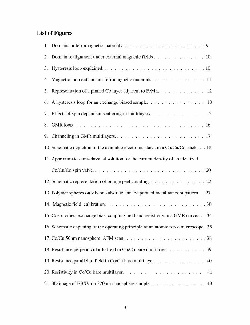
List of Figures
1. Domains in ferromagnetic materials. . . . . . . . . . . . . . . . . . . . . . . 9
2. Domain realignment under external magnetic fields . . . . . . . . . . . . . . 10
3. Hysteresis loop explained. . . . . . . . . . . . . . . . . . . . . . . . . . . . . 10
4. Magnetic moments in anti-ferromagnetic materials. . . . . . . . . . . . . . . 11
5. Representation of a pinned Co layer adjacent to FeMn. . . . . . . . . . . . . 12
6. A hysteresis loop for an exchange biased sample. . . . . . . . . . . . . . . . 13
7. Effects of spin dependent scattering in multilayers. . . . . . . . . . . . . . . 15
8. GMR loop. . . . . . . . . . . . . . . . . . . . . . . . . . . . . . . . . . . . 16
9. Channeling in GMR multilayers. . . . . . . . . . . . . . . . . . . . . . . . . 17
10. Schematic depiction of the available electronic states in a Co/Cu/Co stack. . . 18
11. Approximate semi-classical solution for the current density of an idealized
Co/Cu/Co spin valve. . . . . . . . . . . . . . . . . . . . . . . . . . . . . . . 20
12. Schematic representation of orange peel coupling. . . . . . . . . . . . . . . . 22
13. Polymer spheres on silicon substrate and evaporated metal nanodot pattern. . 27
14. Magnetic field calibration. . . . . . . . . . . . . . . . . . . . . . . . . . . . 30
15. Coercivities, exchange bias, coupling field and resistivity in a GMR curve. . . 34
16. Schematic depicting of the operating principle of an atomic force microscope. 35
17. Co/Cu 50nm nanosphere, AFM scan. . . . . . . . . . . . . . . . . . . . . . . 38
18. Resistance perpendicular to field in Co/Cu bare multilayer. . . . . . . . . . . 39
19. Resistance parallel to field in Co/Cu bare multilayer. . . . . . . . . . . . . . 40
20. Resistivity in Co/Cu bare multilayer. . . . . . . . . . . . . . . . . . . . . . 41
21. 3D image of EBSV on 320nm nanosphere sample. . . . . . . . . . . . . . . 43

4
22. Sectional AFM scan of EBSV on 320nm nanosphere sample. . . . . . . . . 44
23. 3D image of EBSV on 560nm nanosphere sample. . . . . . . . . . . . . . . 45
24. Sectional AFM scan of EBSV on 560nm nanosphere sample. . . . . . . . . 46
25. Resistance perpendicular to field in a bare EBSV sample. . . . . . . . . . . 49
26. Resistance parallel to field in a bare EBSV sample. . . . . . . . . . . . . . . 50
27. Resistivity in a bare EBSV. . . . . . . . . . . . . . . . . . . . . . . . . . . 51
28. A plot of the GMR% vs. minimum resistivity in EBSV samples. . . . . . . . 54
29. Maximum resistivity vs. minimum resistivity in EBSV samples. . . . . . . . 55
30. Minimum resistivity and GMR% vs roughness in EBSV samples. . . . . . . 57
31. Orange peel modeling magnetic coupling in EBSV samples. . . . . . . . . 59
32. Coupling field in the EBSV samples versus RMS roughness. . . . . . . . . 61
33. Orange peel fit to the coupling field with an offset. . . . . . . . . . . . . . 62

5
Abstract
This thesis explores the relationship between substrate roughness and the giant
magnetoresistive properties of exchange biased spin valves and Co/Cu multilayers. For
this purpose controlled roughness is introduced onto Si substrates and the appropriate thin
film structure is sputtered. Giant magnetoresistance is measured and correlated with
atomic force microscopy roughness measurements. Substrate roughness leads to
interfacial roughness which is related to giant magnetoresistance through its effects on
electron scattering and magnetic ordering through oscillatory interlayer exchange,
“orange peel” and pinhole couplings. Results suggest that the dominant effect on giant
magnetoresistance is a decrease due to increasing total film resistivity with higher
roughness. While an increase in magnetic coupling was also observed it seemed to have
no significant effect on giant magnetoresistance in exchange biased spin valves.

6
1 Introduction
“Spintronics” has the potential to revolutionize electronics. The basic idea behind
spintronics is to use the spin of the electron in addition to its charge to regulate currents.
One spin-based effect seen in magnetic thin film multilayers is giant magnetoresistance
(GMR). GMR is a relatively large change in resistance experienced by a multilayer under
the influence of an applied magnetic field. This phenomenon has many important
practical applications.
Sensors based on GMR have allowed an unprecedented increase in hard disk
drive capacity [1]. Significantly better sensitivity of GMR sensors, compared to inductive
sensors, allows for much higher data densities. Another important application is Magnetic
Random Access Memory (MRAM). Such devices may end up revolutionizing
nonvolatile flash storage [2]. Radiation-hardened MRAM also has potential applications
in military and aerospace systems [3].
This thesis explores the effects of interfacial roughness on current in plane GMR.
Past studies of roughness effects have focused on small-scale interfacial roughness
introduced by growth conditions, such as vacuum chamber pressure. There is very little
work done exploring the effect of large scale substrate roughness on interfacial roughness
and GMR. It is important to be able to predict the behavior of GMR structures on novel
substrates with inherent roughness. This will allow for GMR multilayers to be deposited
on a wide variety of materials other than the common silicon wafer. While the main focus
of the project is an exchange biased spin valve, effects of substrate roughness on Co/Cu
mutilayers are also considered.

7
Various magnetic couplings are responsible for GMR in both structures. It is
important to consider the effects of interfacial roughness on these couplings in order to
understand how GMR will be affected. There are also other more subtle consequences of
interfacial roughness on GMR that must be considered. It is important to understand the
individual contributions of these effects on GMR in order to obtain a better
comprehension of the effects of large scale interfacial roughness on GMR.
2 Theory
2.1 Ferromagnetism
Ferromagnetic materials are the basis of GMR. In exchange biased spin valves it
is also important to understand the anti-ferromagnetic properties of materials such as
FeMn. Generally, magnetization in ferromagnetic solids results from the spin orientation
of the electrons in the material. Angular momentum has a much smaller contribution
[11].
Ferromagnetism is a purely quantum mechanical effect resulting from electron-
electron interactions. The total wave function of two electrons in the electron cloud has to
be anti-symmetric due to the Pauli exclusion principle. For a spin triplet state the spatial
wave function will be anti-symmetric providing separation between the electrons and
minimizing the Coulomb repulsion. On the other hand, a spin singlet state will have a
higher energy due to a stronger Coulomb interaction.

8
A simple representation of the interaction energy has the following form,
21int SSE ⋅−= α (1)
where � can be calculated from the Coulomb term in the Hamiltonian and 1S and 2S are
the spins of the two electrons. Note that in ferromagnetic materials � is positive.
Rewriting equation (1) in combined spin basis,
)43
2( 2
2
int �+−= SE α (2)
where S is the total spin of the two electrons. It is clear from equation (2) that it would
be energetically beneficial for the electrons to maximize their total spin by aligning
themselves in the same direction.
Thermal energy of the electrons counteracts to an extent this tendency of spin
alignments. Above a critical temperature the long term order established by the
interaction in (2) is lost. This temperature is referred to as the Curie temperature and for
Co it is 1404K [12]. It is clear that at room temperature we can expect Co electrons to
align.
Aligning all electron spins in the same direction does not provide the lowest
energy configuration in the absence of an external field. Domains, which are sections of
the ferromagnetic material with homogeneous magnetization, form to minimize the total
energy. If we had a single domain magnetostatic energy due to the resulting field would
offset the benefits of minimizing exchange energy. Magnetostatic energy thus favors the

9
presence of more domains that tend to cancel out their magnetic fields. Crystalline
structure also dictates that magnetizing a sample along different direction requires
different external fields. This leads to a preference in the magnetization direction of the
domains. Mangetostrictive energy is the result of changes in the dimensions of the sample
depending on the magnetization. Balancing all the energies mentioned above produces a
complex domain pattern with average domain size of about 10µm [13].
An external field simplifies the situation a bit. Domains that are aligned with the
external field tend to grow at the expense of other domains and eventually the material
obtains a homogeneous magnetization in the same direction as the external field [13].
Figures 1 and 2 illustrate this process.
Figure 1. Domains tend to align with external fields in order to minimize the energy of the system.
(picture obtained from http://hyperphysics.phy-astr.gsu.edu/hbase/solids/ferro.html)
10
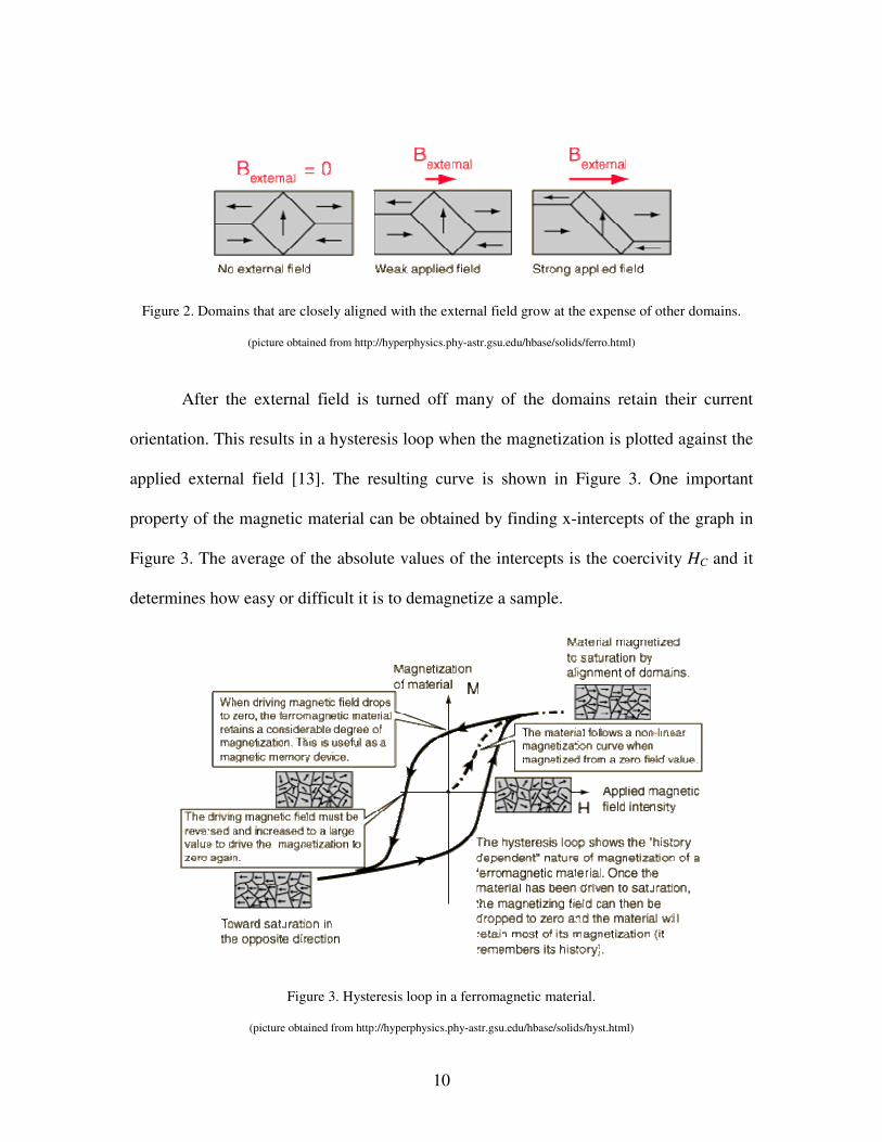
Figure 2. Domains that are closely aligned with the external field grow at the expense of other domains.
(picture obtained from http://hyperphysics.phy-astr.gsu.edu/hbase/solids/ferro.html)
After the external field is turned off many of the domains retain their current
orientation. This results in a hysteresis loop when the magnetization is plotted against the
applied external field [13]. The resulting curve is shown in Figure 3. One important
property of the magnetic material can be obtained by finding x-intercepts of the graph in
Figure 3. The average of the absolute values of the intercepts is the coercivity HC and it
determines how easy or difficult it is to demagnetize a sample.
Figure 3. Hysteresis loop in a ferromagnetic material.
(picture obtained from http://hyperphysics.phy-astr.gsu.edu/hbase/solids/hyst.html)

11
2.2 Anti-Ferromagnetism and Exchange Biasing
Some GMR multilayers use anti-ferromagnetic materials. In anti-ferromagnetic
materials � as introduced in equation (2) is negative resulting in a preference for the spin
singlet electronic state. Just like ferromagnetic materials there exists a critical
temperature beyond which this order is lost. This temperature is called the Neel
temperature and for FeMn it is about 500K [14]. The Fermi structure dictates the anti-
ferromagnetic arrangement schematically shown in Figure 4 [13].
Figure 4. Schematic representation of magnetic moment distribution in an anti-ferromagnetic material.
Anti-ferromagnetic (AFM) materials such as FeMn can be used to “pin” adjacent
ferromagnetic (FM) layers such as Co in GMR multilayers. Pinning is caused by the
exchange bias interactions across the AFM/FM interface. This is achieved by heating the
multilayer close to the Neel temperature of the anti-ferromangetic material but well
bellow the Curie temperature of the ferromagnetic layer and then cooling down the
structure in a uniform magnetic field. The FM layer will align itself with the external
field. This will align the AFM layer magnetic moments, at the AFM/FM interface, with
12
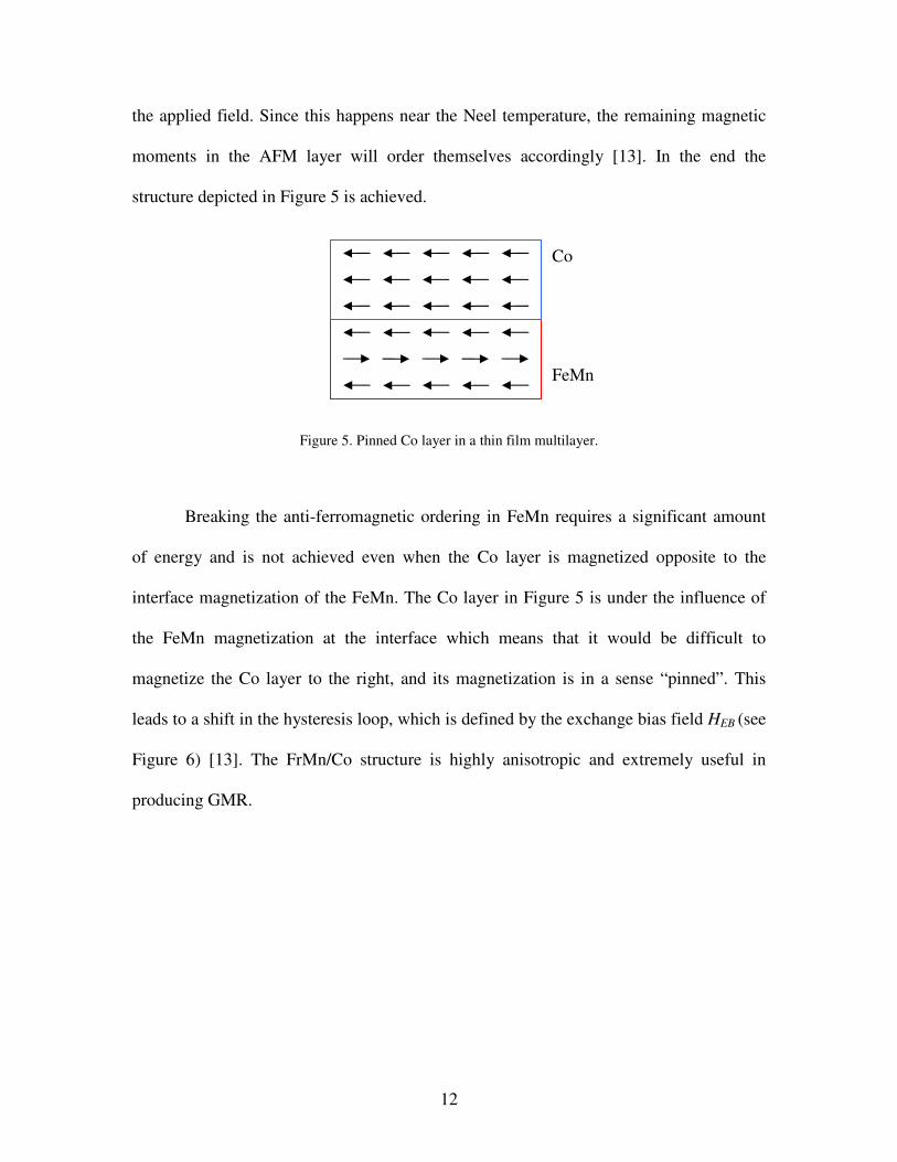
the applied field. Since this happens near the Neel temperature, the remaining magnetic
moments in the AFM layer will order themselves accordingly [13]. In the end the
structure depicted in Figure 5 is achieved.
Figure 5. Pinned Co layer in a thin film multilayer.
Breaking the anti-ferromagnetic ordering in FeMn requires a significant amount
of energy and is not achieved even when the Co layer is magnetized opposite to the
interface magnetization of the FeMn. The Co layer in Figure 5 is under the influence of
the FeMn magnetization at the interface which means that it would be difficult to
magnetize the Co layer to the right, and its magnetization is in a sense “pinned”. This
leads to a shift in the hysteresis loop, which is defined by the exchange bias field HEB (see
Figure 6) [13]. The FrMn/Co structure is highly anisotropic and extremely useful in
producing GMR.
FeMn
Co

13
Figure 6. A hysteresis loop for an exchange biased sample. Coercivity and exchange biased fields
are shown.
HEB
HC HC
H
M

14
2.3 Giant Magnetoresistance
Giant magnetoresistance was first observed in 1988 in Fe/Cr layered structures
[4,5] and has since been seen in a large variety of thin film multilayers. GMR is defined
as a large change in resistance measured in an applied magnetic field. The external field
orientates the magnetizations of the ferromagnetic layers in the multilayers to achieve
parallel and anti-parallel alignment, as shown in Figure 7. The basic process giving rise
to GMR is spin-dependent electron scattering. Current flows through a ferromagnetic (F)
layer with certain magnetization, and depending on the magnetization of the next
ferromagnetic layer, different degrees of electron scattering will occur [6]. See Figure 8
for a sample GMR curve and the magnetization alignments in the different states.
The Camley Barnas theory (CB), which is outlined below, describes the basic
behavior. Let’s consider the simplified multilayer structure of a ferromagnetic material,
conducting (C) spacer layer and another ferromagnetic material. We consider two cases
of alignment of the magnetic moments of the ferromagnetic layers: parallel and anti-
parallel. Assuming all electrons with spin opposite to that of the next layer scatter at the
interfaces we get the following estimate. Electrons with spin that is aligned with the
ferromagnetic moment have a mean free path of roughly 3t (no scattering), where t is the
thickness of each layer. On the other hand, electrons that are anti-aligned with the
magnetic moment of the ferromagnetic layers have a mean free path of t (scatter at both
interfaces). This gives us an average mean free path of 2t when the two ferromagnetic

15
layers are aligned. In the case of the two ferromagnetic layers having opposite magnetic
moments, electrons aligned with either ferromagnetic layer scatter once resulting in a
mean free path of 1.5t. The decrease in mean free path results in an increase in resistivity
for the anti-parallel alignment. This model assumes that the mean free path of the
electron λ in either the spacer or the ferromagnetic material is larger then t which is
indeed the case in the structures considered here.
Figure 7. When the two ferromagnetic layers are aligned spin up electrons have mean free path of 3t and
spin down 1t. This gives us average mean free path of 2t. When the two ferromagnetic layers have opposite
alignment both spin up and spin down electrons have mean free paths of 1.5t and the average mean free
path goes down to 1.5t.
F F F F

16
Figure 8. GMR loop. Plotted is resistivity versus applied field. Depicted are also the schematic
alignments of the ferromagnetic layers.

17
Hood and Falicov describe a different mechanism that enhances the GMR effect
[7]. Consider the case for both ferromagnetic layers aligned with the spin of an electron
in the spacer layer. This electron will be “channeled” through a series of specular
reflections at the interfaces between the spacer layer and the ferromagnetic layers because
the spin bands in the ferromagnetic layers are filled. If the electron spin is anti-aligned
with the magnetic moment of the ferromagnetic layer then it may enter into the more
resistive ferromagnetic material. In the case of the two ferromagnetic materials having
opposing magnetic moments (anti-parallel alignment), little or no “channeling” will occur
(see Figure 9). Thus if the interfaces are smooth and the spacer material has significantly
better conductance then the ferromagnetic material, “channeling” can play an important
role.
Figure 9. Spin up electrons in the spacer layer will travel their normal mean free path as they would be
unable to enter the already filled spin band in the ferromagnetic material (left). This is not the case for the
anti-parallel alignment of the ferromagnetic layers (right) where neither spin up nor spin down electrons, on
average, experience specluar reflection more then once.

18
Let us examine the band structure of Co in order to better understand the
scattering, reflection and transmissions at the interfaces. The density of electron states in
Co that have spins aligned with an external magnetic field is much higher. As the energy
of the states that are anti-aligned with the applied field increases some of these states end
up well above the Fermi energy and are thus practically inaccessible. Thus an incident
electron that has a spin that is anti-aligned with the magnetization of the ferromagnetic
layer it is trying to penetrate is likely to scatter or reflect depending on the exact
incidence angle and energy. Figure 10 shows schematically how this happens.
Figure 10. Schematic depiction of the available electronic states in a Co/Cu/Co stack. Note that
there are very few available spin up electronic states available in the rightmost layer and scattering or
reflection of spin up electrons at the interface is likely.
M
Energy
State Density
Fermi
Energy
M
Energy
State Density
Fermi
Energy
Energy
State Density
Fermi
Energy
Co Co Cu
I

19
A complete theory of GMR involves solving the Boltzmann transport equation.
An exact analytical solution for the current in plane geometry is unavailable. Current
densities for an idealized Co/Cu/Co spin valve are shown in Figure 11. These are
obtained from [15] and are based on a bulk resistivity of 3µ�cm for copper and 15µ�cm
for Co. Among other things, these values suggest that channeling may indeed play an
important role in GMR for near perfect interfaces. Unfortunately this solutions is not very
helpful in realistic spin-valves especially when we factor in the roughness. Still it
provides a good idea of what the current flow roughly is.

20
Figure 11. Approximate semi-classical solution for the current density of an idealized Co/Cu/Co
spin valve. P is the conductivity for the parallel alignment and AP for the anti-parallel. GMC is the
difference responsible for GMR. uu and dd are up and down spin channel conductivity respectively and ud
and du are the conductivities for the AP alignment of the spin up and spin down channels [15].

21
2.4 Magnetic Couplings in Thin Film Multilayers
Maximum GMR effect is achieved when the magnetizations of the ferromagnetic
layers can be aligned in true parallel and anti-parallel configurations. Magnetic coupling
between the ferromagnetic layers thus plays a critical role in GMR. Orange peel coupling
represents an interaction between magnetic poles forming on rough interfaces. Neel’s
model first described this form of coupling [9]. The interlayer coupling energy J is given
by,
λπ
λµπ Cut
pfop e
MMhJ
220
22
2
−= (3)
where h is the peak-peak amplitude of the roughness and λ is the wavelength, Mf and Mp
are the saturation magnetizations of the free and pinned layers respectively and tCu is the
thickness of the Cu spacer layer between the two Co layers experiencing coupling. This
results in a coupling field of:
λπ
λπ
µ
Cut
f
p
ff
opop e
t
Mh
Mt
JH
2222
0 2
−== (4)
where tf is the thickness of the free layer [9]. It is important to notice that equation (4)
tells us that the coupling can be either increasing or decreasing with λ. Figure 12 shows
schematically the interaction responsible for orange peel coupling.

22
Figure 12. Schematic representation of orange peel coupling. Magnetic poles form and couple
with poles in the adjacent ferromagnetic layer through the resulting magnetic fields. A thin spacer layer is
also depicted.
The largest contribution to the oscillatory interlayer exchange coupling comes
from RKKY coupling, named after Ruderman, Kittel, Kasuya and Yosida [8]. Oscillatory
interlayer exchange coupling is responsible for the anti-ferromagnetic coupling which
leads to GMR in Co/Cu superlattice multilayers. In RKKY coupling, spins in one
ferromagnetic layer couple by a local exchange interaction to a conduction electron in the
spacer layer which then transfers to a distant spin in another layer via another local
exchange interaction. The interaction energy is
)/sinh(/
)2
sin()( 0
02
0
00
TTTTt
tkE
J Cu
Cuex ψπµ
+Λ
= (5)
23
where E0 is coupling energy, k0 is wave number � is the wavelength of the coupling
repeating pattern, � is a phase factor, T is the temperature and T0 is a characteristic
temperature [8]. The form of T0 is,
CuB
F
tkπν
2T0
�= (6)
where �F is the Fermi velocity of the relevant electrons in the Cu layer [8]. Consider the
temperature dependant term in (5) with (6) in mind,
0)/sinh(
/lim
0
0
0=
∂∂
→ TTTT
TCut (7).
So for very thin Cu layers the entire temperature dependence term can be treated as a
constant. It is important that the interaction energy in (5) can be negative which results in
an anti-ferromagnetic coupling. The RKKY coupling field is [8],
)/sinh(
/)
2sin(
)( 0
02
0
0
0 TTTTt
tkMtE
MtJ
H Cu
Cuffff
exex ψπ
µ+
Λ== (8).
RKKY coupling amplitude decreases substantially with interfacial roughness in
Co/Cu/Co systems [16].
Pinhole coupling can also be important when interfacial roughness is considered.
Difficult to model, pinhole coupling consists of “ bridges” across the spacer layer that

24
allow for direct coupling between the two ferromagnetic layers. This kind of coupling is
relevant when the spacer layer is thin and the amplitude of the roughness is large. It has a
detrimental effect on GMR since the ferromagnetic layers can not switch independently
and achieve an anti-parallel configuration.
Ignoring pinhole coupling the total coupling field between two ferromagnetic
layers separated by a non-magnetic layer is [8],
opexcoup HHH += (9).
Magnetic couplings are important in understanding the effects of interfacial roughness on
GMR.
2.5 Anisotropic Magnetoresistance
It is important to separate effects of anisotropic magnetoresistance (AMR) from
those of giant magnetoresistance. AMR is observed in single ferromagnetic layers and is
unrelated to the multilayer structure necessary for GMR. If the current is flowing parallel
to the magnetic field applied an increase in resistance is observed with increasing
magnetic field.

25
Measurements indicate that AMR can be described by the following equation,
)1( HeA αρ −−≅∆ (10)
where A and � are parameters. With the magnetic field parallel to the current the
deformed electron clouds offer more resistance to the current carrying electrons. There is
a saturation level as the A parameter in (10) suggests.
The situation is different in the case of the current going perpendicular to the
applied magnetic field. We have:
)1( HeA ⊥−⊥⊥ −≅∆ αρ (11).
In both cases the effect is rather small compared to GMR. The respective parameters in
(10) and (11) have similar values and the sum of (10) and (11) is approximately zero
which is confirmed by experimental data presented bellow.
2.6 Effects of Roughness
Roughness in GMR multilayers can have an effect on GMR through multiple
channels. First of all, roughness can affect the magnetic properties of the ferromagnetic
layers and the couplings between them as discussed previously.
Roughness can also have an effect on GMR through producing more scattering
sites. If these sites produce more spin-dependant scattering, GMR will be enhanced.

26
However if the additional scattering leads to spin flipping it may decrease further spin
dependent scattering and channeling resulting in a decrease in GMR.
Finally roughness can increase spin independent scattering which will lower the
relative strength of the GMR effect. This will be observed as an increase of the overall
resistivity of the sample. Additional spin independent scattering can decrease the mean
free paths significantly resulting in higher resistivity. Intermixing of the multilayers as a
result of roughness can further increase the overall resistivity of the samples. While this
will not affect the difference in resistivity between the anti-parallel and the parallel states
it will change its relative magnitude as compared to the overall resistivity of the sample.

27
3 Experiment
3.1 Rough Substrates
In order to introduce uniform roughness onto smooth substrates, we spin coat
nanospheres, which are basically latex balls, of varying diameters onto standard 2”
silicone wafers. Ideally this results in a single layer of nanospheres attached to the
silicone substrate (see Figure 13). We used nonspheres with diameter
50,99,160,190,250,320,460 and 560nm. Two nanosphere sizes, 50nm and 460nm, are
used for Co/Cu stacks and three samples are prepared for each nanosphere size listed
above with the exchange biased spin valve structure.
Figure 13. a) Polymer spheres on silicon substrate, b) Evaporated metal nanodot pattern. (Obtained from Dr. Jianjun Wang, AS William and Mary)

28
After spin coating the nanospheres, 15nm of Au is evaporated onto the sample.
Au impinges on the substrate through the gaps remaining between the nanospheres. Then
the substrate is placed in a difloromethane sonic bath for 10-15 minutes. This washes the
nanospheres away and leaves Au “ triangles” on the surface of the Si (Figure 13).
3.2 Giant Magnetoresistive Multilayers
Two different structures were used in this experiment, an exchange biased spin
valve (ESBV) and a superlattice (many period) multilayer. The EBSV has the following
structure: Nb3nm/Cu5nm/Co4nm/Cu4nm/Co4nm/FeMn10nm/Cu3nm/Nb2nm.
Niobium is used to facilitate crystalline growth on the substrate and to prevent oxidation.
Notice that the FeMn, which is an anti-ferromagnetic material, is grown on the top of the
structure. This is done in order to avoid unwanted effects of the substrate roughness on
the pinning of the adjacent Co. Due to the anisotropic behavior of the pinned Co layer we
can obtain both parallel and anti-parallel alignment of the two Co layers depending on the
external magnetic field. The second structure which is studied in much less detail is a
Co/Cu multilayer.
The multilayers have the following structure:
Nb3nm/[Cu5nm/Co4nm]x10/Cu10nm/Nb2nm. Niobium serves the same purpose as in
the EBSV. RKKY coupling is responsible for GMR in this structure. Recall that (5)
suggests that the Co layers can be coupled antiferromagnetically. This is the case with the
Co/Cu multilayer. As the external field increases some of the Co layers switch and align
themselves with the external field as their neighboring anti-ferromagnetically coupled Co

29
layers remain magnetized opposite to the field resulting in high resistance. As the field
increases further the anti-ferromagnetic coupling is overcome and all the layers align with
the magnetic field resulting in lower resistance.
The ½ x ½” films grown for this experiment were produced by sputtering in a
vacuum chamber at Michigan State University. The vacuum chamber was initially
evacuated to a pressure of about 1 x 10⁻⁹ Torr and then the polycrystalline films were
grown at room temperature in argon gas at a pressure of roughly 1 mTorr. The EBSV
samples were pinned by heating them to 180°C and then cooling them in a uniform
magnetic field.
3.3 Giant Magnetoresistive Measurements
For the GMR measurements, the samples are placed in a holder between the poles
of an electromagnet (GMW 3470 Electromagnet, driven by Kepco BOP 50-4D 4886
bipolar power supply) which provides the applied magnetic field.

30
-30
-20
-10
0
10
20
30
-0.6 -0.4 -0.2 0 0.2 0.4 0.6
Magnet Calibration
y = -0.61329 + 59.008x R= 0.99983 M
agne
tic F
ield
[mT]
Current [A] Figure 14. Magnetic Field as a function of applied field.
Let us first consider magnet calibration. Figure 14 shows the measured field as a
function of the applied current. As expected the fit is linear but there is a slight offset at
zero field due to coercivity of the magnet and Earth’s magnetic field.
A custom built 4-point probe sample holder is used, for resistance measurements,
which eliminates the need for solder joints. The sample stage supplies four connections
with the circumference of the sample through Pogo-25B-6 gold plated contacts. The

31
resistance is measured by applying a constant current along one edge of the sample and
measuring the voltage drop across the other parallel edge. A Keithley 4ZA4 Sourcemeter
provides the current (10 mA) through the sample via two of the four contacts. A
HP3401A multimeter measures the voltage drop along the other two contacts. We use a
computer running LabView to drive the experiment and record the data. Two
measurements are made for each sample so that we can compute resistivity with the van
der Pauw method. Maximum field is held for 5 seconds to ensure proper initial
magnetization and then is cycled down to a minimal value and back. Each of the three
EBSV samples for each nanosphere sizes is measured separately.
We used the van der Pauw method for measuring and calculating resistivity [10].
There are some conditions that must be satisfied for this approach to work: contacts must
be at the circumference of the sample; contacts must be sufficiently small; sample must
be homogeneous in thickness; and surface of the sample must be singly connected.
When these conditions are satisfied, the following equation gives the resistivity,
)/(2)2ln( ,,
,,DABCCDAB
DABCCDAB RRfRRd +
= πρ (12).
In equation (12) ρ is the resistivity, d is the thickness of the sample, RAB,CD is the voltage
drop along AB divided by the current flowing through CD and RBC,DA is the voltage drop
along BC divided by the current flowing through DA. A, B, C and D are the points of
contact along the circumference of the sample. Note that in (12) we are taking an average
of the resistance measured parallel and perpendicular to the field which will average out
the AMR in the final resistivity value.

32
The function f is determined by
fe
arRR
RR f
DABCCDAB
DABCCDAB
���
�
�
���
�
�
=+−
2cosh
2ln
,,
,, (13).
Unfortunately this transcendental equation is not very useful. A good approximation
when RAB,CD ≅ RBC,DA is
���
����
�−�
�
�
�
��
�
�
+−
−��
�
�
��
�
�
+−
−≅12
)2(ln2
)2(ln22ln
132
4
,,
,,
2
,,
,,
DABCCDAB
DABCCDAB
DABCCDAB
DABCCDAB
RR
RR
RR
RRf (14).
The error in the power series expansion in (14) does not exceed
���
����
�−�
�
�
�
��
�
�
+−
12)2(ln
2)2(ln 32
4
,,
,,
DABCCDAB
DABCCDAB
RR
RR (15).
So with the above equations in mind we can obtain the resistivity of a sample from two
perpendicular resistance measurements.

33
The following paragraphs briefly discuss how data is extracted from the GMR
plots. We can measure coercivity of the free (HCF) and pinned layers (HCP), maximum
(�max) and minimum resistivity (�min) of the sample, exchange biasing (HEB) of the pinned
layer and coupling between the ferromagnetic layers (HCOUP). While some of the
quantities are apparent from the graph some require an explanation. The pinned layer will
switch away from zero field due to its exchange bias, while the free layer switches near
zero field. Any offset of the switching of the free layer is the effect of coupling between
the two ferromagnetic layers. Maximum and minimum resitivities are easily obtained
from the curve and GMR% is calculated by
min
minmax% ρ
ρρ −=GMR (16).
We can obtain the coercivities, exchange bias and coupling field as shown in Figure 15.
The measurements of all the magnetic properties are made at 2
minmax ρρ +.
GMR plots of exchange biased spin valves (EBSV) contain sections that look like
parts of hysteresis loops. In an EBSV one Co layer is pinned with the help of FeMn and
the other is left “ free” to rotate magnetization which allows for the desired anti-parallel
alignment. The fields at which the pinned and free layers switch are different depending
on their previous magnetization. Going through Figure 15, we start on the right, with both
layers magnetized to the right. As the field decreases, the pinned layer under the
influence of the adjacent anti-ferromagnetic switches magnetization to the left. This
happens at HEB – HCP. This results in the anti-parallel alignment and a sharp increase in

34
GMR as the switch occurs. Then as the field further decreases the free layer also switches
to the left at HCOUP - HCF resulting in parallel alignment and decrease in GMR. On the
way back as the field increases, the free layer switches to the right, this time at HCOUP +
HCF, resulting in anti-parallel alignment and again increase in GMR. At HEB + HCP the
pinned layer switches again to the right resulting in a decrease in GMR. So without any
explicit hysteresis loop measurements we can obtain most important magnetic properties
of both layers. Unfortunately we can not obtain anything more than the resistivity from
the Co/Cu stacks used in a part of this experiment.
1.06 10-6
1.065 10-6
1.07 10-6
1.075 10-6
1.08 10-6
1.085 10-6
1.09 10-6
1.095 10-6
1.1 10-6
-600 -400 -200 0 200 400 600
EBSV on 250nm Nanosphere Substrate
Res
istiv
iy [O
hm m
]
Magnetic Field [Gauss]
Figure 15. Reading off coercivities, exchange bias, coupling field and resistivity from an EBSV curve.
2HCP 2HCF
HEB
HCOUP
Pinned Layer Switches
Free Layer Switches
35
3.4 Roughness Measurements
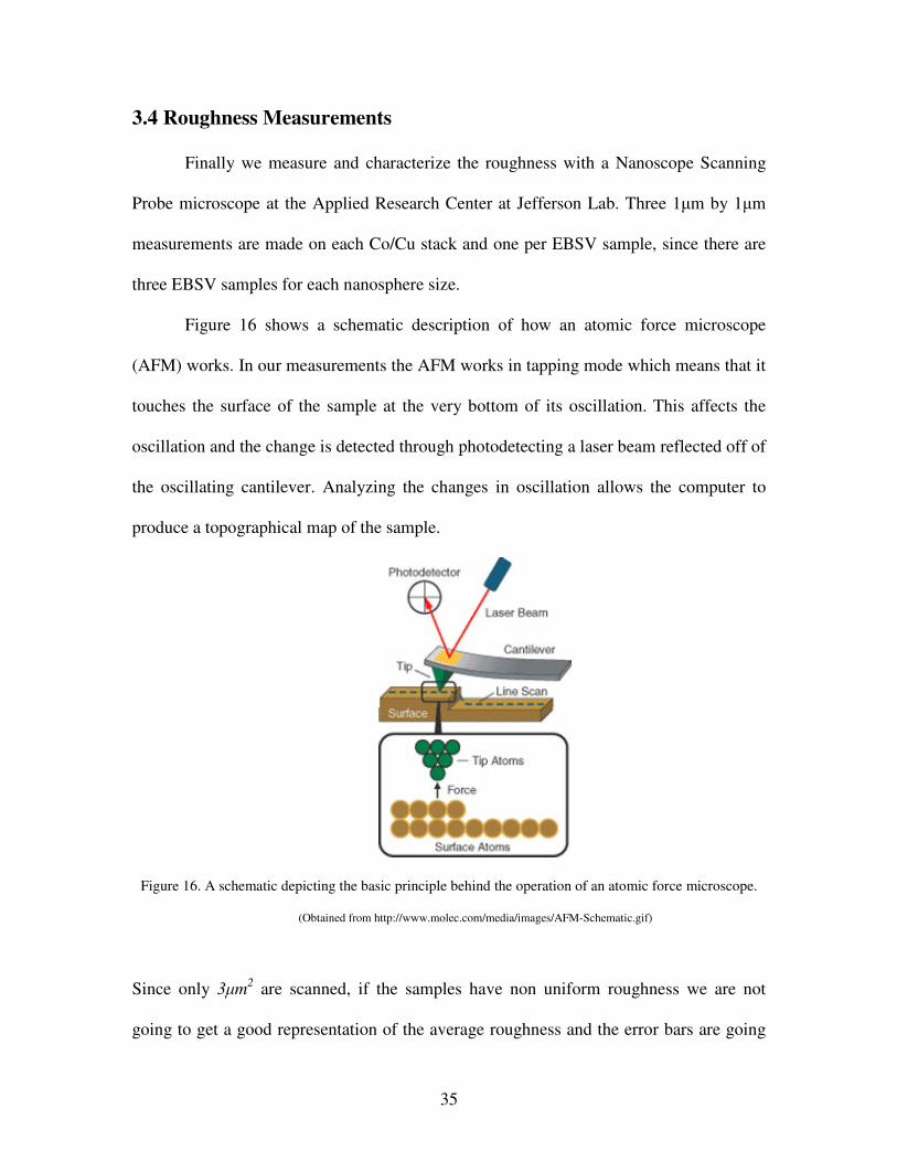
Finally we measure and characterize the roughness with a Nanoscope Scanning
Probe microscope at the Applied Research Center at Jefferson Lab. Three 1�m by 1�m
measurements are made on each Co/Cu stack and one per EBSV sample, since there are
three EBSV samples for each nanosphere size.
Figure 16 shows a schematic description of how an atomic force microscope
(AFM) works. In our measurements the AFM works in tapping mode which means that it
touches the surface of the sample at the very bottom of its oscillation. This affects the
oscillation and the change is detected through photodetecting a laser beam reflected off of
the oscillating cantilever. Analyzing the changes in oscillation allows the computer to
produce a topographical map of the sample.
Figure 16. A schematic depicting the basic principle behind the operation of an atomic force microscope.
(Obtained from http://www.molec.com/media/images/AFM-Schematic.gif)
Since only 3�m2 are scanned, if the samples have non uniform roughness we are not
going to get a good representation of the average roughness and the error bars are going

36
to be high. This would not be a problem if we get the anticipated uniform nanodot
pattern.
3.5 A Note on Error Bars
All measurement errors and error bars presented in this thesis are standard errors
in the mean. The relationship between the standard error in the mean and a standard
deviation is,
NSEM
σ= (17)
where SEM is the standard error in the mean, � is the standard deviation and N is the
number of measurements. SEM propagates in the same manner as �. SEM gives us 95%
confidence that the actual mean is within an SEM from the measured mean.
4 Results
4.1 Co/Cu Multilayer Data and Analysis
Co/Cu multilayers were studied to see the effects of substrate roughness on a
system with multiple interfaces. Table 1 summarizes the measurements. Unfortunately
the desired nanodot pattern was not observed in any of the Co/Cu samples due to
difficulties with spin coating a single layer of nanospheres onto the Si. Figure 17 shows
the second AFM scan for the 50nm nanospheres. The other scans look similar. Some of

37
the scans also suggest that the nanospheres were not completely removed by the
difloromethane. While the desired structure is not present some Au still found its way
onto the Si and non-uniform roughness is observed as the data in Table 1 suggests.
Unfortunately this also means large error bars since the roughness is non-uniform.
Structure RMS Roughness
[nm]
Standard Error
in Roughness
[nm]
ρmin
[Ohm m]
ρmax
[Ohm m]
GMR
[%]
Reference 2.8407 0.5286 9.721e-8 1.0623e-7 9.2836
50nm 4.6590 0.665617 1.3012e-7 1.3745e-7 5.6309
460nm 10.602 3.189747 1.2977e-7 1.3625e-7 4.9919
Table 1. Summary of Co/Cu multilayer data. GMR % decreases with roughness.

38
Figure 17. Co/Cu 50nm nanosphere, AFM scan. No nanodots unfortunately which suggests more
then one layer of nanospheres was spin coated.
Errors associated with the resistivity calculations are listed in Table 2. These are minor
and have no significant effect on the data. The ferr comes directly from equation (15) and
is a consequence of the difference of resistance along and perpendicular to the applied
field. Bdiff is the difference in actual field between any two points used for computing the
resistivity. While the current set points are the same in both plots the actual current
measured and resulting field varies somewhat between measurements. Both Bdiff and ferr
are the maximum values of all the plot points. Figures 18, 19 and 20 show the original
resistance plots and the calculated resistivity plot for Co/Cu bare substrate respectively.

39
Structure ferr [%] Bdiff [G]
Reference .024 .73
50nm .014 1.1
460nm .003 .37
Table 2. Summary of errors in ρ calculations. Both numbers are maximums from the calculations of all
points (about 400 per plot).
0.25
0.255
0.26
0.265
0.27
0.275
0.28
-800 -600 -400 -200 0 200 400 600 800
Bare Co/Co Resistance GMR Plot
Res
ista
nce
[Ohm
]
Field [Gauss]
Figure 18. Voltage drop divided by applied current measured perpendicular to the field.
40
0.16
0.165
0.17
0.175
0.18
-800 -600 -400 -200 0 200 400 600 800
Bare Co/Cu Transverse Resistance GMR PlotR
esis
tanc
e [O
hm]
Field [Gauss]
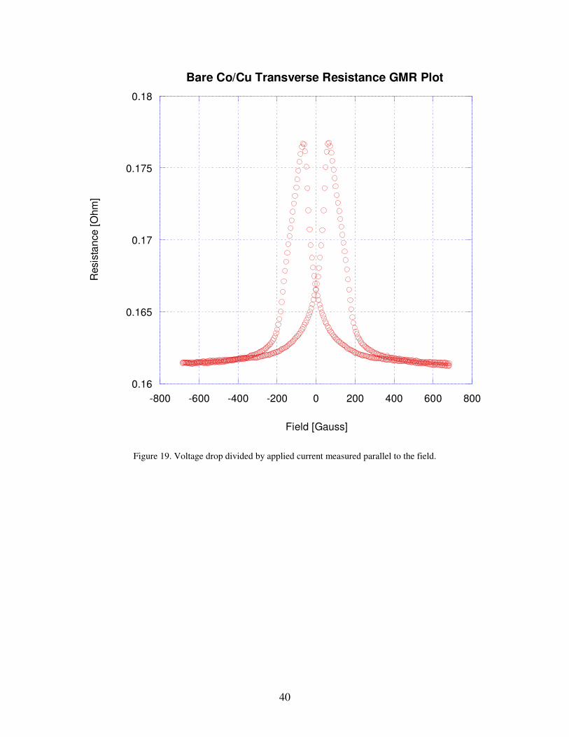
Figure 19. Voltage drop divided by applied current measured parallel to the field.

41
9.6 10-8
9.8 10-8
1 10-7
1.02 10-7
1.04 10-7
1.06 10-7
1.08 10-7
-800 -600 -400 -200 0 200 400 600 800
Bare Co/Cu Resistivity GMR PlotR
esis
tivity
[Ohm
m]
Field [Gauss]
Figure 20. Calculated resistivity for Co/Cu stack on a bare substrate.
Note the slight effects of AMR on the GMR plots in Figures 18 and 19 near zero field.
These do not affect the measurements in Table 1 and are not even noticeable when
averaged out in Figure 20.
Table 1 suggests most of the decrease in GMR comes from the increased sample
resistivity with increasing roughness. The difference between maximum and minimum
resistivity is on average about .076 10-8 �m. A contributing factor to that decrease in
GMR is also the slight decrease in the difference between maximum and minimum

42
resistivity coming most likely from orange peel magnetic coupling between the layers
and decreasing RKKY antiferromagnetic coupling. In a Co/Cu multilayer the antiparallel
alignment is heavily dependent on the magnetic couplings and their effect on GMR is
noticeable. Unfortunately there is no way to obtain these magnetic properties from the
GMR plots.
4.3 EBSV Data
EBSV were used because in this structure a true anti-parallel state can be
achieved. The majority of data for this experiment came from the EBSVs for two reasons.
There are 27 EBSV samples with 8 different nanosphere sizes used compared to 3 Co/Cu
samples with 2 nanosphere sizes used. Second there are a number of magnetic properties
that we can obtain from the GMR plots of EBSV that are unavailable in Co/Cu GMR
plots. Let us start by analyzing the roughness data.
4.3.1 EBSV Roughness Data
Unfortunately out of 27 EBSV structures only 2 showed the desired nanodot
structure. Data from the third 320nm nanosphere EBSV sample is shown in Figures 21
and 22.

43
Figure 21. 3D image of the EBSV deposited on top of the nanodot pattern obtained from a 320nm
nanospheres.

44
Figure 22. Sectional analysis of the EBSV deposited on top of the nanodot pattern obtained from a 320nm
nanospheres. Horizontal spacing is slightly larger then expected at 359.38nm but not unreasonable.
Data from the 560nm nanospheres AFM scans is shown in Figures 23 and 24.

45
Figure 23. 3D image of the EBSV deposited on top of the nanodot pattern obtained from a 560nm
nanospheres.

46
Figure 24. Sectional analysis of the EBSV deposited on top of the nanodot pattern obtained from a 560nm
nanospheres. Horizontal spacing is slightly smaller then expected at 553.09 nm.
The cross sections show that we are indeed looking at the nanodots. Data from the other
samples is used but is highly non-uniform resulting in large error bars. Table 3 shows the
AFM results from all EBSV samples.

47
Structure RMS Roughness [nm] Standard Error [nm]
Reference 4.4887 1.2602
50nm 4.6590 0.66562
99nm 7.3997 0.75684
160nm 10.981 4.9574
190nm 6.8183 2.4014
250nm 12.026 4.8637
320nm 17.064 9.1586
460nm 9.5060 2.3420
560nm 20.341 7.2914
Table 3. RMS Roughness of the EBSV samples.
Notice that the lower the roughness the lower the error in Table 3. This is to be expected
as the low RMS roughness suggests that little Au made its way onto the substrate and
therefore the surface is relatively uniform.

48
4.3.2 Resistivity Calculations and Magnetic Properties of EBSV Samples
Table 4 lists the errors associated with the resistivity calculations. These are again
minor and average out in the calculation of the standard error in the mean for each of the
quantities.
Structure ferr [%] Bdiff [G]
Reference 0.049517 0.654485
50nm 0.059088 0.695945
99nm 0.109344 0.450143
160nm 0.039454 0.530103
190nm 0.306787 0.245802
250nm 0.151169 0.571564
320nm 0.154781 0.571564
460nm 0.206782 0.530103
560nm 0.060368 0.533065
Table 4. Errors associated with the resistivity calculation. The error in f is due to an approximation in the
van der Pauw method and the difference in field comes from the measurements.
Figures 25, 26 and 27 show the resistance, transverse resistance and resistivty curves for
the 560nm nanosphere EBSV sample.

49
0.94
0.95
0.96
0.97
0.98
0.99
1
1.01
-600 -400 -200 0 200 400 600
Resistance Perpendicular to Field Bare EBSVR
esis
tanc
e [O
hm]
Field [Gauss]
Figure 25. Resistance perpendicular to field for reference EBSV sample. Notice that the peak around zero
is higher then the other one due to AMR.

50
1.58
1.6
1.62
1.64
1.66
1.68
1.7
-600 -400 -200 0 200 400 600
Res
ista
nce
[Ohm
]
Field [Gauss]
Resistance Parallel to Field Bare EBSV
Figure 26. Resistance parallel to field for reference EBSV sample. Notice that the peak around zero is
lower then the other one due to AMR.

51
5.8 10-7
5.9 10-7
6 10-7
6.1 10-7
6.2 10-7
6.3 10-7
-600 -400 -200 0 200 400 600
Res
istiv
ity [O
hm m
]
Field [Gauss]
Resistivity Bare EBSV
Figure 27. Calculated resistivity plot for reference EBSV sample. Notice that the peak around zero the
same height as the other peak.
One important thing is apparent from Figures 25, 26 and 27, AMR indeed cancels out as
expected. The peak around zero is about the same height as the other one in the resistivity
plot which is not the case in the resistance plots.

52
One advantage of the EBSV is that we can extract a multitude of data on the
magnetic properties of the structure from the GMR plot. Table 5 lists these.
Structure HCF
[G]
HCFError
[G]
HPF
[G]
HPFError
[G]
HEB
[G]
HEBError
[G]
HCoup
[G]
HCoupError
[G]
Reference 54.604 4.1903 49.707 3.0270 197.05 5.2107 1.2180 0.84141
50nm 32.053 1.5165 49.447 1.8420 197.63 3.2108 25.313 1.0488
99nm 38.793 3.5542 60.162 5.9052 181.47 3.7360 49.797 3.8542
160nm 39.538 2.7561 58.581 4.7944 189.34 12.578 49.589 4.2674
190nm 36.012 2.0703 60.781 1.9994 199.32 5.4356 51.427 2.9318
250nm 33.988 1.9521 54.955 2.6710 194.07 5.6153 32.233 1.8601
320nm 58.805 5.9739 89.112 3.8419 191.70 0.92626 24.742 5.2832
460nm 30.367 1.7135 42.067 3.0050 192.30 3.3697 18.588 1.9877
560nm 32.784 1.0188 47.773 5.1539 209.22 4.1477 20.590 3.4919
Table 5. Magnetic properties of the EBSV samples and their respective errors.
The data in Table 5 confirms that the exchange bias is for all intensive purposes
unaffected by the roughness. This was the idea behind depositing the FeMn on top of the
structure. Coercivities of the free and pinned layers vary significantly due to domain
structure changes and couplings associated with the roughness. Coupling field varies
quite a bit as well due to orange peel, RKKY and pinhole couplings. Data is obtained
through linear interpolation and errors are the standard errors in the mean based on the
three samples for each nanosphere size. Further analysis of the data follows bellow.

53
4.3.3 Electric Properties of EBSV Samples
Data on the electric properties of the EBSV samples is presented in this section.
Table 6 contains all the relevant quantities and their errors.
Structure �min
[��cm]
�minError
[��cm]
�max
[��cm]
�maxError
[��cm]
�
[��cm]
�Error
[��cm]
GMR
[%]
GMRError
[%]
Reference 5.9850 .046403 6.3448 .046666 .35976 .0018016 6.0116 0.045983
50nm 13.864 .79370 14.184 .78942 .32017 .032410 2.3295 0.21522
99nm 16.714 1.3092 17.096 1.3523 .38259 .079673 2.2773 0.11704
160nm 19.270 .63144 19.682 .64321 .41178 .061476 2.1381 0.17649
190nm 14.318 .33040 14.579 .32004 .26079 .071718 1.8277 0.31095
250nm 9.8973 .37090 10.234 .38222 .33716 .020550 3.4077 0.040402
320nm 18.150 .70702 18.362 .70535 .21283 .025995 1.1771 0.097875
460nm 7.7223 .29600 8.0561 .29622 .33376 .0058756 4.3341 0.16360
560nm 8.3776 .40108 8.7504 .39783 .37278 .025223 4.4752 0.30948
Table 6. Electric properties of EBSV samples and associated errors.
The decrease in GMR is proportional to the increase in overall resistivity and no
significant changes are observed in �. The resistivity values are very reasonable
compared to the resistivity of Co 15��cm and Co 3 ��cm for the bulk materials.

54
4.4 EBSV Data Analysis
Let us look at some plots of the data listed above and explore the relationships
between the quantities. First let us look at a plot of the GMR% versus minimum
resistivity (Figure 28). GMR% is by definition,
minmin
minmax%ρ
ρρ
ρρ ∆≡−
≡GMR (18).
1
2
3
4
5
6
7
5 10-7 1 10-6 1.5 10-6 2 10-6
GMR% vs Minimum Resistivity in EBSV Samples
GM
R
Minimum Res
y = m1/m0ErrorValue
1.3372e-073.4473e-06m1 NA1.2664ChisqNA0.96698R
Figure 28. A plot of the GMR% vs. minimum resistivity.

55
So assuming constant � we would have a 1/�min relationship. This seems to be the case
in Figure 28 with � = .3447±.0134 ��cm. This is in excellent agreement with the data
in Table 6 suggesting that the effects on GMR are indeed dominated by the effects of
roughness on overall resistivity. To further confirm this point let us look at the plot of the
maximum resistivity vs. minimum resistivity in Figure 29.
6 10-7
8 10-7
1 10-6
1.2 10-6
1.4 10-6
1.6 10-6
1.8 10-6
2 10-6
5 10-7 1 10-6 1.5 10-6 2 10-6
Maximum vs Minimum Resistivity in EBSV
Max
imum
Res
isiti
viy
[Ohm
m]
Minimum Resistivity [Ohm m]
y = m1 + m2 * M0
ErrorValue6.4149e-093.6186e-08m1 0.00475080.99767m2
NA2.9917e-16ChisqNA0.99992R
Figure 29. Maximum resistivity vs. minimum resistivity in EBSV samples.
The slope is, within the error, equal to 1. This is exactly what we would expect if overall
resistivity was solely responsible for the changes in GMR. The y-intercept is simply � =
56
.3619±.0641 ��cm in excellent agreement with the value obtained in Figure 28 and the
data in Table 6.
With this in mind let us look at the effects of roughness on resistivity and GMR.
Figure 30 suggests a weak oscillatory relation between roughness and resistivity. It would
be difficult to model this with confidence due to the large errors in the roughness
measurements. It is safe to say that the first drop in GMR% is most likely the result of
decreased channeling. With roughness at the interfaces we do not expect any significant
channeling to occur in the Cu layer which results in a sharp increase in the resistivity and
decrease in GMR.

57
1
2
3
4
5
6
7
5 10-7
1 10-6
1.5 10-6
2 10-6
0 5 10 15 20 25
GMR% and Minimum Resistivity vs Roughness
GMR Minimum ResistivityG
MR
[%]
Minim
um R
esistivity [Ohm
m]
RMS Roughness [nm]
Figure 30. Minimum resistivity and GMR vs roughness in EBSV samples. Error bars are omitted to
declutter the plot and line are a guide to the eye.
Next let us examine the magnetic coupling between the layers. We do not expect
any major contribution of the coupling to the GMR as the data above shows. Strong
coupling fields could lower GMR but obviously at the current scales this is a minor
effect, requiring a higher precision experiment.
Exploring the relationship between the roughness and coupling is intriguing in itself and
could provide predictions in cases when its effects on GMR are not negligible. Let us

58
model the coupling field using the orange peel theory alone first. This is not unreasonable
since the thickness of the spacer layer varies very little if at all with the roughness. Any
variation in that thickness would be the result of sputtering Cu on a rough surface. Figure
31 shows two curve fits to the data. Surprisingly the curve that assumes constant vertical
roughness is a better fit. There are two possible explanations for that. The first one is that
the error in the RMS roughness is so high that using it to model coupling is not possible.
The second possibility is that neglecting the RKKY contribution to the coupling is not
appropriate. Before we explore the second option let us see if the fit parameters make
sense. Saturation magnetization Mp for the pinned Co layer is roughly going to be the
saturation magnetization for bulk Co which is 18000 Gauss. The thickness of the free
layer tf is 4nm. Examining the m2 parameter in the smooth curve fit in Figure 31
suggests that the observed wavelength is .3127±.0343 times the nanosphere size. From
pure geometrical consideration in an ideal nanodot pattern we would expect that value to
be ½ and this does not seem unreasonable. With this in mind and using equation (4) again
we obtain that the average vertical RMS roughness is 0.135±.010nm. This seems low and
suggests that we either need the residual RKKY and potentially pinhole coupling
contributions included or that the roughness is lower than the measurements suggest.
Although precautions were taken to prevent that from happening, measurements can be

59
affected from dust on the surface and impurities introduced through sputtering.
0
10
20
30
40
50
60
-100 0 100 200 300 400 500 600
Orange Peel Coupling ModelC
oupl
ing
[Gau
ss]
Nanosphere Size [nm]
y = h^ 2*m1/M0*exp(-m2/M0)
ErrorValue3.61288.5649m1 57.954141.13m2
NA1188.9ChisqNA0.70064R
y = m1/M0*exp(-m2/M0)ErrorValue154714628m1
12.437113.67m2 NA254.7ChisqNA0.94389R
Figure 31. Orange peel modeling of the coupling. The smooth curve assumes constant vertical roughness
(as a fit parameter) and is represented be the table on the left. The piecewise smooth curve takes into
account measured vertical roughness and is described by the table on the right.

60
The piecewise smooth fit in the table on the right of Figure 31 is not analyzed as it
fits the data poorly. While the plot in Figure 32 suggests that there might be an oscillatory
relationship between the vertical RMS roughness and the coupling, one look at the
uncertainties tells us that it would be difficult to obtain a curve fit with any confidence. It
actually proved very difficult to obtain a fit with the RKKY theory added. Even when a
fit was obtained it was much worse then the one for orange peel effect alone. This is in
agreement with theory and RKKY effects are indeed not substantial when roughness is
introduced [16]. One last improvement to Figure 31 can be made. Introducing an offset to
the curve fit improves it. This offset is in a sense an average RKKY, pinhole coupling for
all the samples. Figure 33 shows this curve fit. If the offset is indeed negative as the
parameter m3 suggests then it must be predominately the result of anti-ferromagnetic
RKKY coupling. The error in m3 is large so the only thing that we can conclude with
certainty is that there is no significant, if any, pinhole coupling. This curve fit gives us a
wavelength to nanosphere size ratio of 0.311±.031 and an average RMS roughness of
0.142±.014. The slight increase in roughness is encouraging as the offset factor can now
account for what appears to be a weak anti-ferromagnetic coupling which allows a higher
orange peel coupling resulting from higher roughness.

61
0
10
20
30
40
50
60
70
80
4 8 12 16 20 24 28
Cou
plin
g [G
auss
]
RMS Roughness [nm]
Coupling Field vs RMS Roughness in EBSV Samples
Figure 32. Coupling field in the EBSV samples versus RMS roughness. The error bars are too large to
obtain a meaningful curve fit. Lines are a guide to the eye.

62
0
10
20
30
40
50
60
-100 0 100 200 300 400 500 600
Orange Peel Coupling Model with OffsetC
oupl
ing
[Gau
ss]
Nanosphere Size [nm]
y = m1/M0*exp(-m2/M0)+m3ErrorValue265916347m1 11.57114.41m2
5.1067-4.1508m3 NA229.42ChisqNA0.94961R
Figure 33. Orange peel fit to the coupling field with an offset.

63
5 Conclusions and Future Work
We have produced a series of Co/Cu EBSV and multilayers on a variety of rough
substrate surfaces. Data for both Co/Cu stacks and EBSV suggests that the entire
decrease in GMR% is the result of increasing resistivity. Unfortunately if there is a
corresponding increase in interfacial, spin dependent scattering it is beyond the precision
of the current experiment.
Producing a uniform controlled roughness proved more difficult then anticipated.
As a result it is difficult to make direct models of the relationships between sample
resistivity and vertical roughness. The case was similar for coupling field and vertical
roughness. It is however reasonable to expect that roughness will increase the resistivity
and decrease GMR in the samples.
While the coupling fields had small if any effects on GMR better understanding
their behavior in rough samples is also of significant importance. In an EBSV significant
ferromagnetic coupling can occur between the layers before GMR is affected. This is a
direct consequence of the about 200 Gauss exchange bias and layer coercivities of about
30-60 Gauss. In Co/Cu multilayer we observed a small decrease in � which is to be
expected as a consequence of the decrease in RKKY and increase in orange peel
couplings. The anti-parallel state is not fully achieved and GMR suffers. In general it
appears that EBSV are more robust and would work better on novel, rough, substrates
then Co/Cu stacks.
Orange peel effect seemed to account well for the coupling measured in EBSV
samples. It suggested a very reasonable value for the wavelength to nanosphere size ratio
64
and a somewhat low value for the average RMS vertical roughness. As the desired
nanodot pattern was not achieved we can only conclude that while the roughness may be
periodic in nature it is very non-uniform in height and when averaged out over the entire
sample not as large as anticipated. Since we only measure a cross section of about 3�m2
this is possible.
In the end the experiment would have been much more successful with the
nanodot structure but even in this form the data suggests some interesting conclusions. In
the future it would be great to be able to study the effects of roughness on coupling and
sample resistivity with more precision in order to be able to model them and through
them to model GMR. One conclusion that will likely remain the same is that the
dominant effect of interfacial roughness is an increase in overall resistivity which leads to
a decrease in GMR and that the orange peel effect is the major contribution to magnetic
coupling between the ferromagnetic layers.

65
Bibliography
[1] IBM Research, “ The Giant Magnetoresistive Head: A giant leap for IBM
Research” , http://www.research.ibm.com/research/gmr.html
[2] J. Robert Lineback, “ Motorola reaches 4-Mbit milestone in development of
nanocrystal memory as flash replacement” , The Semiconductor Reporter (2003)
http://www.semireporter.com/public/2840.cfm
[3] “ Honeywell licenses Motorola's MRAM for SOI-based radiation-hard ICs” (2003)
http://www.semireporter.com/public/4704.cfm
[4] M. N. Baibich et al., Phys. Rev. Lett. 61, 2472 (1988).
[5] G Binasch et al., Phys. Rev. B 39, 2428 (1989).
[6] R. E. Camley and J. Barnas, Phys. Rev. Lett. 63, 664 (1989).
[7] R. Q. Hood and L. M. Falicov, Phys. Rev. B 49, 368 (1994).
[8] C-L. Lee et al., J. Appl. Phys. 91, 7113 (2002)
[9] L. Neel, Comptes. Rendus 255, 1676 (1962).
[10] L. J. van der Pauw, Philips Res. Reports 13, 1-9 (1958).
[11] M.N. Rudden and J. Wilson, Elements of Solid State Physics (Wiley, New York,
1993), Second Ed., p. 98.
[12] J.R. Hook, and H.E. Hall, Solid State Physics, (John Wiley and Sons, New York,
1991), Second Ed., p. 220.
[13] Nicola Spaldin, Magnetic Materials, (Cambridge University Press, Cambridge,
2003), p. 75-106.
[14] F. Canet et al., Europhys. Lett., 52 (5), 594-600 (2000).

66
[15] W.H. Butler, X.-G. Zhang, and J.M. MacLaren, Journal of Superconductivity:
Incorporating Novel Magnetism, Vol. 13, No. 2, 2000, p. 221-238.
[16] J. Kudrnovsky et al., J. Phys.: Condens, Matter 13, 8539 (2001)

67
Acknowledgments
First of all I would like to thank my advisor Dr. Reilly for all her help with the
project. She gave me many opportunities over the last few years to get a head start on my
thesis and guided me through the many frustrations of experimental research.
I would like to thank graduate student Shannon Watson for all her help with the
project. She did most of the spin coating, and multilayer deposition for the samples used
in this thesis. Our many discussions on the project and the theory were also invaluable.
I would like to also thank Olga Trofimova at the Applied Research Center at
Jefferson Lab for guiding me through the AFM measurements and all her help. Last but
not least I would like to thank the committee members for taking the time to evaluate this
project.

68
Appendix I – LabView Virtual Instruments’ Snapshots
Main data collection VI. Includes three sub-programs, four step sequence structure and communicates with
the power supply and voltmeter.
Resistivity VI. Takes two GMR plots obtained with the previous VI and outputs a single resistivity file.
Based on the van der Pauw method. Includes one sub-program.


![1 Interfacial Rheology System. 2 Background of Interfacial Rheology Interfacial Shear Stress Interfacial Shear Viscosity = [ ]](https://img.dokumen.tips/doc/110x75/56649d1f5503460f949f3d29/1-interfacial-rheology-system-2-background-of-interfacial-rheology-interfacial.jpg)