Embed Size (px)
Citation preview
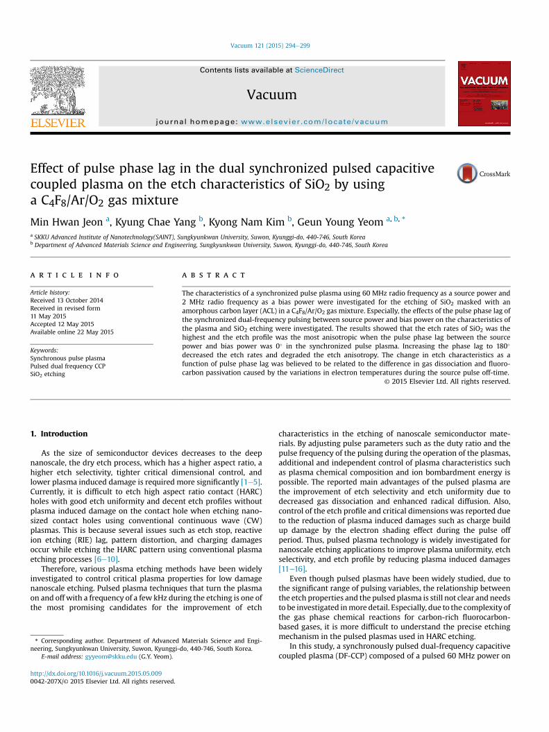
lable at ScienceDirect
Vacuum 121 (2015) 294e299
Contents lists avai
Vacuum
journal homepage: www.elsevier .com/locate/vacuum
Effect of pulse phase lag in the dual synchronized pulsed capacitivecoupled plasma on the etch characteristics of SiO2 by usinga C4F8/Ar/O2 gas mixture
Min Hwan Jeon a, Kyung Chae Yang b, Kyong Nam Kim b, Geun Young Yeom a, b, *
a SKKU Advanced Institute of Nanotechnology(SAINT), Sungkyunkwan University, Suwon, Kyunggi-do, 440-746, South Koreab Department of Advanced Materials Science and Engineering, Sungkyunkwan University, Suwon, Kyunggi-do, 440-746, South Korea
a r t i c l e i n f o
Article history:Received 13 October 2014Received in revised form11 May 2015Accepted 12 May 2015Available online 22 May 2015
Keywords:Synchronous pulse plasmaPulsed dual frequency CCPSiO2 etching
* Corresponding author. Department of Advancedneering, Sungkyunkwan University, Suwon, Kyunggi-
E-mail address: [email protected] (G.Y. Yeom).
http://dx.doi.org/10.1016/j.vacuum.2015.05.0090042-207X/© 2015 Elsevier Ltd. All rights reserved.
a b s t r a c t
The characteristics of a synchronized pulse plasma using 60 MHz radio frequency as a source power and2 MHz radio frequency as a bias power were investigated for the etching of SiO2 masked with anamorphous carbon layer (ACL) in a C4F8/Ar/O2 gas mixture. Especially, the effects of the pulse phase lag ofthe synchronized dual-frequency pulsing between source power and bias power on the characteristics ofthe plasma and SiO2 etching were investigated. The results showed that the etch rates of SiO2 was thehighest and the etch profile was the most anisotropic when the pulse phase lag between the sourcepower and bias power was 0� in the synchronized pulse plasma. Increasing the phase lag to 180�
decreased the etch rates and degraded the etch anisotropy. The change in etch characteristics as afunction of pulse phase lag was believed to be related to the difference in gas dissociation and fluoro-carbon passivation caused by the variations in electron temperatures during the source pulse off-time.
© 2015 Elsevier Ltd. All rights reserved.
1. Introduction
As the size of semiconductor devices decreases to the deepnanoscale, the dry etch process, which has a higher aspect ratio, ahigher etch selectivity, tighter critical dimensional control, andlower plasma induced damage is required more significantly [1e5].Currently, it is difficult to etch high aspect ratio contact (HARC)holes with good etch uniformity and decent etch profiles withoutplasma induced damage on the contact hole when etching nano-sized contact holes using conventional continuous wave (CW)plasmas. This is because several issues such as etch stop, reactiveion etching (RIE) lag, pattern distortion, and charging damagesoccur while etching the HARC pattern using conventional plasmaetching processes [6e10].
Therefore, various plasma etching methods have been widelyinvestigated to control critical plasma properties for low damagenanoscale etching. Pulsed plasma techniques that turn the plasmaon and off with a frequency of a few kHz during the etching is one ofthe most promising candidates for the improvement of etch
Materials Science and Engi-do, 440-746, South Korea.
characteristics in the etching of nanoscale semiconductor mate-rials. By adjusting pulse parameters such as the duty ratio and thepulse frequency of the pulsing during the operation of the plasmas,additional and independent control of plasma characteristics suchas plasma chemical composition and ion bombardment energy ispossible. The reported main advantages of the pulsed plasma arethe improvement of etch selectivity and etch uniformity due todecreased gas dissociation and enhanced radical diffusion. Also,control of the etch profile and critical dimensions was reported dueto the reduction of plasma induced damages such as charge buildup damage by the electron shading effect during the pulse offperiod. Thus, pulsed plasma technology is widely investigated fornanoscale etching applications to improve plasma uniformity, etchselectivity, and etch profile by reducing plasma induced damages[11e16].
Even though pulsed plasmas have been widely studied, due tothe significant range of pulsing variables, the relationship betweenthe etch properties and the pulsed plasma is still not clear and needsto be investigated inmore detail. Especially, due to the complexity ofthe gas phase chemical reactions for carbon-rich fluorocarbon-based gases, it is more difficult to understand the precise etchingmechanism in the pulsed plasmas used in HARC etching.
In this study, a synchronously pulsed dual-frequency capacitivecoupled plasma (DF-CCP) composed of a pulsed 60 MHz power on

M.H. Jeon et al. / Vacuum 121 (2015) 294e299 295
the top electrode as the source power and a pulsed 2MHz power onthe bottom electrode as the bias power to the substrate was usedwith a C4F8/Ar/O2 gas mixture for the highly anisotropic etching ofnanoscale SiO2 contact. Especially, the effect of the pulse phase lagbetween the source power and the bias power on the plasmacharacteristics and the etching characteristics was investigated tostudy the effect of synchronized pulsing using a dual pulsed plasmaon the etch characteristics of HARC.
2. Experiment
The experimental setup for the synchronized pulse DF-CCPsystem used in this study is shown in Fig. 1. The rf discharge wasmaintained between two parallel plate electrodes separated by30 mm. The top electrode was covered with a perforated siliconplate to flow gases uniformly and was connected to a 60 MHz rfpower (high frequency; HF) source which could be pulsed to con-trol the plasma characteristics and to control the pulse signal delayof the 2 MHz (low frequency; LF) pulsed rf power applied to thesubstrate. The synchronization of 2 MHz rf power to 60 MHz rfpower was achieved by connecting the 60 MHz pulse signal to thedigital delay generator (DDG 645, SRS), to the signal generator(8657B, HP), and to the rf power amplifier (A1000, ENI) in series.Therefore, the source power pulse served as a master and the biaspower pulse served as a slave by receiving the source pulse signalfrom the DDG. The reactor was evacuated by turbo molecularpumps (3200 l/s) backed by a dry pump. The gas was equallydistributed through a baffle system from the top electrode. Thepulse signal generated from the 60 MHz was also used to controlthe time-resolved optical emission spectrometer (OES) installed inthe process chamber.
The 2 mm thick SiO2 deposited on silicon wafers was maskedwith a 600 nm thick amorphous carbon layer (ACL). The ACL wasused as the hardmask for SiO2 HARC etching to maintain the criticaldimension (CD) of the contact hole. The SiO2 layer was etchedfor various pulse parameters during synchronized pulsing with aC4F8/Ar/O2 gas mixture (60 MHz HF power/2 MHz biasvoltage ¼ 300 W/- 900 V, C4F8/Ar/O2 ¼ 40/155/5 sccm, and a pro-cess pressure of 26.6 mbar) while keeping the substrate tempera-ture at room temperature.
Etch characteristic such as the etch rate of SiO2 HARC layer/ACLand the etch profiles using the C4F8/Ar/O2 gas mixture were
Fig. 1. Schematic diagram of the synchronized pulse dual-frequency CCP. A Pulsed60 MHz source pulse power was applied to the top electrode to control the plasmacharacteristics and a pulsed 2 MHz bias power was applied to the bottom electrode tocontrol the ion energy to the substrate.
estimated by field emission scanning electron microscopy (FE-SEM,Hitachi S-4700). The radicals that dominantly affected the etchingwere observed using time-resolved OES. The time-resolved OES(Andor istar 734) was performed with a spectrometer composed ofa grating monochromator and an intensified charge coupled device(ICCD). For the time-resolved data collection, the OES data werecollectedwith the interval of 100 ms in 1 kHz of pulse period and thedata were averaged after 10 collections. The instant change in theelectron temperature for the synchronized pulse conditions of 60/2 MHz DF-CCP was calculated using a home-made emissive probe.Also, the chemical binding characteristics of the etched SiO2 surfacefor the differently synchronized pulse conditions were observedusing X-ray photoelectron spectroscopy (XPS, ESCA2000, VGMicrotech Inc.).
3. Results and discussion
While pulsing with only the 60 MHz source power without the2 MHz bias power in the C4F8/Ar/O2 gas mixture, the plasma den-sity decreased exponentially when the rf power was turned offduring the pulse-off time, due to the lack of rf power to the plasma.The gas molecules and atoms dissociated in the plasma during thepulse on-time, as CFx and F tend to recombine. In our study, inaddition to the 60MHz source power, the 2MHz bias power appliedto the substrate was synchronously pulsed with the source powerand the effect of the pulse phase lag between the source rf powerpulsing and the 2 MHz bias power pulsing on the plasma charac-teristics was investigated. Fig. 2 shows a cartoon figure of thesynchronized pulse waveform for the pulse phase lags between thesource power pulsing and the bias power pulsing during the syn-chronously pulsed 60/2 MHz CCP. As shown in the figure, the phaselag of the bias power pulse to the source power pulse was variedfrom 0� to 180�.
Fig. 3 shows the time-resolved optical emission intensity ratiosfor F/Ar, CF2/Ar, CF3/Ar, and CF2/Ar measured as a function of pulse
Fig. 2. Schematic diagram of pulse waveform between the source power pulsing andthe bias power pulsing for various pulse phase lags in the synchronized pulse 60/2 MHz CCP.

M.H. Jeon et al. / Vacuum 121 (2015) 294e299296
phase lag from 0� to 180� for the DF-CCP using a C4F8/Ar/O2 gasmixture. As the optical emission peak intensities, the peak in-tensities observed at 703 nm, 245e265 nm, 265e285 nm, and751 nm were used for F, CF2, CF3, and Ar, respectively. The opticalemission intensity ratios of the dissociated radicals to Ar were usedto estimate the radical concentration in the plasma. For the time-resolved OES, 300 W of 60 MHz rf power and �900 V of 2 MHz rfvoltage were used with the gas flow rates of C4F8/Ar/O2 ¼ 50/145/5sccm and at 26.6 mbar of operating pressure. The pulse duty ratioand the pulse frequency were kept at 50% and 1 kHz, respectively.The OES data for the CW power condition of both the source powerand the bias power (that is, 60 MHz CW source power/2 MHz CWbias power) is also included as references in Fig. 3(a). As shown inFig. 3(a), when the source power and the bias power were notpulsed, the radical concentrations of CFx(x ¼ 2, 3) and F remained
Fig. 3. Optical emission intensity ratios of CFx(x ¼ 2,3)/F, F/Ar, and CFx (x ¼ 2,3)/F in the synchof pulse phase lags using a time-resolved OES. 300 W of 60 MHz rf power and �900 V of 2 M26.6 mbar of operating pressure. The pulse duty ratio and the pulse frequency were kept at 5the source power and the bias power were pulsed together with (b) the pulse phase lag ofsource power/2 MHz CW bias power.
similar without variations in the time. However, when both thesource and bias power were pulsed together with the pulse phaselag of 0� as shown in Fig. 3(b), the radical densities and the ratios ofCFx (x¼ 2, 3)/F during the pulse on-time (0e500 ms) for both powersources were similar to those observed when both powers wereturned on in Fig. 3 (a). However, during the initial source power off-time (500e600 ms), F radicals decreased more rapidly than otherradicals such as CF2 and CF3. Therefore, the ratios of CFx (x ¼ 2,3)/Fincreased during the initial source power pulse off-time, indicatingenhanced recombination of the dissociated gas mixtures. The ratioremained similar during the rest of the pulse-off time(600e1000 ms).
When the source power and the bias power were pulsed withthe pulse phase lag of 90� during the initial source power on-timeof 0e250 ms, only 60 MHz rf power was applied to the source,
ronously pulsed plasmas. The intensities of CF2, CF3, and F were measured as a functionHz rf voltage were used with the gas flow rates of C4F8/Ar/O2 ¼ 50/145/5 sccm and at
0% and 1 kHz, respectively. (a) 60 MHz CW source power/2 MHz CW source power. Both0� , (c) pulse phase lag of 90� , and (d) pulse phase lag of 180� . (e) is for 60 MHz pulsed

Fig. 4. Instant variation in electron temperature estimated as a function of time for theCW plasma and synchronized pulse phase lag of 0� , 90� , and 180� at the pulse dutypercentage of 50% and pulse frequency of 1 kHz. 155sccm of Ar was used as the gas andthe other conditions are the same as those in Fig. 3.
M.H. Jeon et al. / Vacuum 121 (2015) 294e299 297
without the 2 MHz bias power to the substrate. As shown inFig. 3(c), possibly due to the low frequency of the 2 MHz bias powerwhich tends to give more power to the incident ions than to theplasma, no significant change in F and CFx (x ¼ 2,3) (or only slightincreases in F and slight decreases in CFx) were observed during the0e250 ms compared to the rest of the source power/bias power on-time (250e500 ms). However, as shown in Fig. 3(c), because the2 MHz bias power was still on during the 500e750 ms, a slowerdecrease in F density was observed after the initial source power-off. Therefore, the ratios of CFx(x ¼ 2, 3)/F were lower during thesource pulse off-time (500e1000 ms) compared to during thesource pulse off-time in Fig. 3(b). When the source power and thebias power were pulsed with the pulse phase lag of 180� as shownin Fig. 3(d), the radicals and ratios of CFx(x¼ 2, 3)/F observed duringthe source power on-time were similar to those observed for thesource power on-time (0e500 ms) shown in Fig. 3 (a) and (b).However, when the source power was off (500e1000 ms), thereduction in F density during the source power off-time was thesmallest because the 2 MHz bias power was active during thesource power off-time. Therefore, the ratio of CFx(x ¼ 2,3)/F duringthe source power off-time was also the lowest. As a reference, theradical concentrations of CFx(x¼ 2, 3), F, and the ratios of CFx(x¼ 2,3)/F were measured for the condition with only the source powerpulsing without the bias power (that is, 60 MHz pulsed sourcepower/2 MHz CW bias power) and the results are shown inFig. 3(e). As shown, the radical concentrations of CFx (x¼ 2, 3) and Fand the ratios of CFx(x ¼ 2, 3)/F were similar to those observed forthe condition with the pulse phase lag of 180� shown in Fig. 3(d).These results were observed not only for the source power off-timebut also for the source power on-time (or only slight increases in Fduring the source pulse on-time) possibly due to the low contri-bution of the 2 MHz bias power to the gas dissociation mentionedabove. Therefore, the ratios of CFx(x ¼ 2, 3)/F measured during thesource power off-time was decreased with the increase in pulsephase lag from 0� to 180�.
To understand the gas dissociation characteristics observed inFig. 3 for the conditions with/without pulsing of the source and biaspowers and for the conditions with the different pulse phase lags,the variation of instant electron temperature for the differentpulsing conditions was investigated with an emissive probe. Tomeasure the electron temperature with the emissive probe, only Arwas used as the process gas. Except for that, the conditions weresimilar to the conditions for Fig. 3: that is, 300 W of 60 MHz rfpower to the source, -900 V of 2 MHz rf power to the substrate,26.6 mbar of operating pressure, and 155sccm Arwere used. For thepulsing, 50% of the pulse duty ratio and 1 kHz of pulse frequencywere used. In the emissive probe, time varying plasma potentials(Vp) and floating potentials (Vf) were measured and the instantelectron temperature (Te) was calculated from the followingequation:
Vp � Vf ¼kTe2e
ln�2Mpm
�
where, k is Boltzmann constant, Te is the electron temperature,m isthe electron mass, and M is the Ar atomic mass. The measuredresults for different pulse phase lag conditions in Fig. 3 are shown inFig. 4. The results for the CW power conditions for both the sourcepower and the bias power (that is, 60MHz CW source power/2MHzCW bias power) were also included. As shown in the figure, whenboth the source power and the bias power are in the CW condition,the electron temperature remained at about 7.2 eV. However, whenthe source power and the bias powerwere pulsed together with thepulse phase lag of 0�, the exponential decrease of instant electrontemperature from 7 eV to about 1 eV after 500 ms was observed due
to the lack of power application to the source after 500 ms. Whenthe pulse phase lag was 90�, the instant electron temperaturedecreased from about 7 eV to only about 5 eV until 750 ms. After750 ms, due to the lack of power application to the source, theinstant electron temperature decreased further with time until1000 ms. When the pulse phase lag was 180�, the instant electrontemperature during the source power off-time remained at about5 eV.
The above results show that, when the source power was on(0e500 ms), the instant electron temperature did not changesignificantly whether the bias power was on or not due to thehigher power input to the plasma by the 60 MHz source powercompared to that by the 2 MHz bias power. However, when thesource power was turned off (500e1000 ms), the instant electrontemperature was significantly dependent on whether the bias po-wer was on or off. The higher the electron temperature, the higherthe gas dissociation; therefore, the higher ratios for CFx(x ¼ 2, 3)/Fobtained in Fig. 3 for the decreased pulse phase lag (180� / 0�)appear to be related to the decreased gas dissociation due toreduced bias power to the plasma during the source power pulseoff-time (500e1000 ms).
Using the different pulse phase lag conditions investigated inFig. 3, SiO2 masked with a 600 nm thick amorphous carbon layer(ACL) was etched and the etch profiles observed by FE-SEM areshown in Fig. 5. The etching conditions are the same as those inFig. 3. The etch depth of SiO2 was kept similar at about 1 mm. Theetch rates for SiO2 decreased with increased pulse phase lag,therefore, more etch time was required to etch 1 mm deep SiO2. Inaddition, as shown in the figure, as the pulse phase lag becamesmaller (180� / 0�), the remaining ACL on the SiO2 becamethicker and the SiO2 etch profile became more anisotropic. Theincreased anisotropic SiO2 etch profile, shown in Fig. 5 with thesmaller pulse phase lag, appears to be related to the higher fluo-rocarbon polymer passivation of the sidewall during the sourcepower off-time (500e1000 ms) while etching the SiO2 with moredirectional reactive ions during the source power on-time(0e500 ms). During SiO2 etching masked with ACL, insufficientfluorocarbon polymer passivation results in an increase in the CDof the ACLmask and the ACLmask profile is more sloped due to theincreased ACL etching. The increased ACL mask opening increasesthe top opening CD of SiO2 etch profile and decreases the bottomopening CD of SiO2 etch profile, possibly due to themore scattering

Fig. 5. Etch profiles of ACL masked SiO2 contact hole pattern observed by FE-SEM afterthe etching as a function of synchronous pulse phase lag of 0�/180� with pulse dutypercentage of 50% and pulse frequency of 1 kHz. The etch profile for the source powerpulsing/CW bias power is also shown. The etch time of SiO2 contact hole was varied toobtain about 1 mm of etch depth. The process conditions are the same as those in Fig. 3.
Fig. 6. XPS narrow scan data of C 1s during the depth profiling of the etched SiO2
surface with the pulse phase lag of 0� and 180� and the source power pulsing/CW biaspower pulsing. SiO2 samples were etched to 1 mm of etch depth in the 60/2 MHz CCP.The process conditions are the same as those in Fig. 3.
M.H. Jeon et al. / Vacuum 121 (2015) 294e299298
of the reactive ions entering the SiO2 contact hole during theetching. As the pulse phase lag decreased, as shown in Fig. 3, theCFx(x ¼ 2, 3)/F increased during the source power off-time.Therefore, more fluorocarbon polymer passivation could be ob-tained during the source power off-time. Consequently, the mostanisotropic etch profile was obtained with the pulse phase lag of0�. In Fig. 5, the SiO2 etch profile for the source power pulsing/CWbias power is also shown as a reference. As shown in the figure, theremaining ACL thickness was the lowest and the SiO2 etch profilewas the least anisotropic with a sloped bottom area. This may be aresult of having the lowest CFx(x ¼ 2, 3)/F and the lowest fluoro-carbon polymer passivation during the source power off-time asshown in Fig. 3(b).
The thickness of the fluorocarbon passivation during the etchingfor different pulse phase lags was estimated by XPS depth profilingof the etched SiO2 surface and by measuring the narrow scan dataof C1s. The etch conditions are the same as those in Fig. 5. XPSdepth profiling data were collected four times (total 120s) aftersputtering the etched SiO2 surface for 30s with an Arþ ion gun (3 kVenergy and 2 mA ion current). The results are shown in Fig. 6 for thepulse phase lag of 0 and 180�. As a reference, the XPS depthprofiling data of C1s for the SiO2 etching with the source powerpulsing/CW bias power are also included. As shown, a thickerfluorocarbon passivation layer was observed for the pulse phase lagof 0� compared to the pulse phase lag of 180�. Also, the SiO2 surfaceetched with the pulse source power pulsing/CW bias power, whichhad the worst SiO2 etch profile in Fig. 5, had the thinnest fluoro-carbon passivation layer. Therefore, the improved SiO2 etch profileobtained with the lower pulse phase lag (180�/ 0�) is believed tobe related to the increased fluorocarbon polymer passivation dur-ing the source power pulse off-time.
4. Conclusions
The effect of pulse phase lag between the 60 MHz source powerapplied to the top electrode and the 2 MHz bias power applied tothe bottom substrate during synchronized dual pulsing with 60/2 MHz CCP on the plasma characteristics and the etch character-istics of SiO2 was investigated using a C4F8/Ar/O2 gas mixture. Theconcentrations of dissociated radicals such as CFx (x ¼ 2, 3) and Fwere related to the source power pulsing rather than the bias
M.H. Jeon et al. / Vacuum 121 (2015) 294e299 299
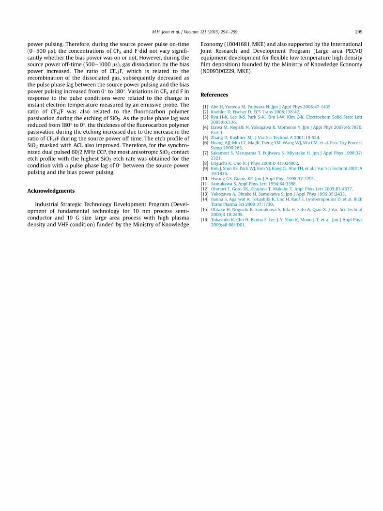
power pulsing. Therefore, during the source power pulse on-time(0e500 ms), the concentrations of CFx and F did not vary signifi-cantly whether the bias power was on or not. However, during thesource power off-time (500e1000 ms), gas dissociation by the biaspower increased. The ratio of CFx/F, which is related to therecombination of the dissociated gas, subsequently decreased asthe pulse phase lag between the source power pulsing and the biaspower pulsing increased from 0� to 180�. Variations in CFx and F inresponse to the pulse conditions were related to the change ininstant electron temperature measured by an emissive probe. Theratio of CFx/F was also related to the fluorocarbon polymerpassivation during the etching of SiO2. As the pulse phase lag wasreduced from 180� to 0�, the thickness of the fluorocarbon polymerpassivation during the etching increased due to the increase in theratio of CFx/F during the source power off time. The etch profile ofSiO2 masked with ACL also improved. Therefore, for the synchro-nized dual pulsed 60/2 MHz CCP, the most anisotropic SiO2 contactetch profile with the highest SiO2 etch rate was obtained for thecondition with a pulse phase lag of 0� between the source powerpulsing and the bias power pulsing.
Acknowledgments
Industrial Strategic Technology Development Program (Devel-opment of fundamental technology for 10 nm process semi-conductor and 10 G size large area process with high plasmadensity and VHF condition) funded by the Ministry of Knowledge
Economy (10041681, MKE) and also supported by the InternationalJoint Research and Development Program (Large area PECVDequipment development for flexible low temperature high densityfilm deposition) founded by the Ministry of Knowledge Economy(N009300229, MKE).
References
[1] Abe H, Yoneda M, Fujiwara N. Jpn J Appl Phys 2008;47:1435.[2] Koehler D, Fischer D. ECS Trans 2008;138:47.[3] Ryu H-K, Lee B-S, Park S-K, Kim I-W, Kim C-K. Electrochem Solid State Lett
2003;6:C126.[4] Izawa M, Negishi N, Yokogawa K, Momonoi Y. Jpn J Appl Phys 2007;46:7870.
Part 1.[5] Zhang D, Kushner MJ. J Vac Sci Technol A 2001;19:524.[6] Huang AJJ, Min CC, Ma JK, Tseng YM, Wang WJ, Wu CM, et al. Proc Dry Process
Symp 2006:263.[7] Sakamori S, Maruyama T, Fujiwara N, Miyatake H. Jpn J Appl Phys 1998;37:
2321.[8] Eriguchi K, Ono K. J Phys 2008;D 41:024002.[9] Kim J, Shin KS, Park WJ, Kim YJ, Kang CJ, Ahn TH, et al. J Vac Sci Technol 2001;A
19:1835.[10] Hwang GS, Giapis KP. Jpn J Appl Phys 1998;37:2291.[11] Samukawa S. Appl Phys Lett 1994;64:3398.[12] Ohmori T, Goto TK, Kitajima T, Makabe T. Appl Phys Lett 2003;83:4637.[13] Yokozawa A, Ohtake H, Samukawa S. Jpn J Appl Phys 1996;35:2433.[14] Banna S, Agarwal A, Tokashiki K, Cho H, Rauf S, Lymberopoulos D, et al. IEEE
Trans Plasma Sci 2009;37:1730.[15] Ohtake H, Noguchi K, Samukawa S, Iida H, Sato A, Qian X. J Vac Sci Technol
2000;B 18:2495.[16] Tokashiki K, Cho H, Banna S, Lee J-Y, Shin K, Moon J-T, et al. Jpn J Appl Phys
2009;48:08HD01.