Embed Size (px)
Citation preview
ELSEVIER Journal of Non-Crystalline Solids 220 (1997) 63-68
J O U R N A L OF
Effect of heat treatment on the optical properties of amorphous S b z S 3 film: the possibility of optical storage
P. Arun, A.G. Vedeshwar * Department of Physics and Astrophysics, University of Delhi, Delhi 110 007, India
Received 6 August 1996; revised 29 April 1997
Abstract
The optical absorbance, refractive index and absorption edge of vapour deposited amorphous Sb2S 3 films are studied systematically as a function of annealing temperature in the range 160°C > T > 23°C. As deposited films continuously loose sulphur above 60°C as determined by ESCA and this loss affects their measured optical properties. Modification of optical properties upon heating to T = 160°C opens the possibility of a WORM (write once read many times) kind of optical storage as demonstrated in laser irradiation experiment. © 1997 Elsevier Science B.V.
1. Introduction 2. Experimental
Amorphous chalcogenide thin-films have a poten- tial for optical storage applications [1]. Such films can be prepared by vapour deposit ion onto cold substrates. Chalcogenides can be reversibly cycled between the amorphous and crystall ine states [1,2] by laser irradiation. The molecular structure manifesta- tions of photo-induced or thermally induced transfor- mations of amorphous chalcogenide thin-films are of general interest. The effect of heat treatment may promote chemical ordering, alter the molecular struc- ture by a local rearrangement of atoms or change the number of defects in films [3]. In the present work we have examined the effect of heat treatment on vapour deposited amorphous Sb2S 3 films to explore the potential of the material for photo-thermal optical storage applications.
* Corresponding author. E-mail: [email protected].
The Sb2S 3 films were grown on thin (0.1 mm) glass substrates at room temperature by vacuum ( < 10 -5 Torr) evaporation using crystalline SbzS 3 as a starting material in a molybdenum boat. As grown films were amorphous as revealed by X-ray diffraction studies (Philips PWI840) . Most of the as grown films were stoichiometric. However, some films were found to be slightly antimony rich, i.e., Sbl00 xSx with x = 59, as established by ESCA (electron spectroscopy for chemical analysis ) analy- sis (Shimadzu, MgK~x). Thin film samples of 4 × 4 mm area were heat treated in air at temperatures T, in the range 23°C < T < 160°C for about 2 0 - 3 0 s at each temperature using a copper block. ESCA analy- sis with depth profile was carried out for all fi lms to determine their composit ion as a function of anneal- ing temperatures. Films of 300 nm thickness were used throughout this study. ESCA depth profiles of such films revealed uniform composition. The opti-
0022-3093/97/$17.00 © 1997 Elsevier Science B.V. All rights reserved. PII S0022-3093(97)00229-9
64 P. Arun, A. G. Vedeshwar / Journal of Non-Crystalline Solids 220 (1997) 63-68
533 eV
,°3/2 ( \ s s~2 ev Sb / ,, 1 164 ev
I I Ix,41 I I
550 533eV 528 170 160 Binding Energy (eV)
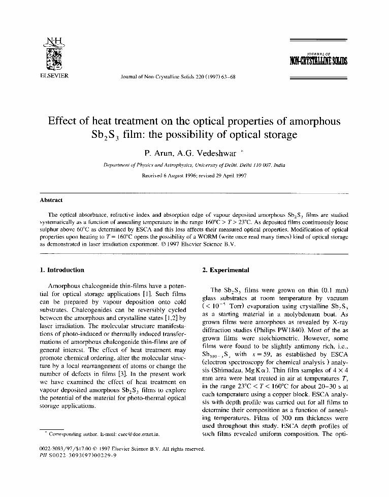
Fig. 1. X-ray photo-electron spectra of 3000 A thick Sbl00_xS x films at (i) room temperature (as grown), (ii) annealed at 80°C and (iii) 100°C. The thickness of the film is the same throughout this study.
cal absorption (or transmission) of the films in the visible and near IR region was measured using a spectrophotometer (Shimadzu 260). The substrate's absorption was corrected (by the instruments com- puter interface) by taking measurements with refer- ence to another similar glass slide. We have used a continuous Argon ion laser (Coherent's Innova 70-4) to irradiate the as grown films. The primary aim of the present study was to examine changes in optical properties of such films with temperature and to explore possible applications for optical storage. Compositional and structural studies were carried out to understand their role on optical properties.
3. Results
3.1. Compositional analysis
Fig. l shows selective photo-electron spectra of amorphous Sbl00_xS x films taken as a function of annealing temperature. Chemical composition x of the amorphous films could be determined using the integrated area under the sulphur 2p~/2 and anti- mony 3d5/2 peaks normalized to their scattering cross sections. Although the films were treated in air, our ESCA results show no evidence of oxygen, in films heat treated up to 160°C. Specifically the O ls peak close to Sb 3d5/2 peak was not detected [4]. In
Fig. 2 we plot the sulphur content of the films with annealing temperature.
3.2. Atomic scale structure
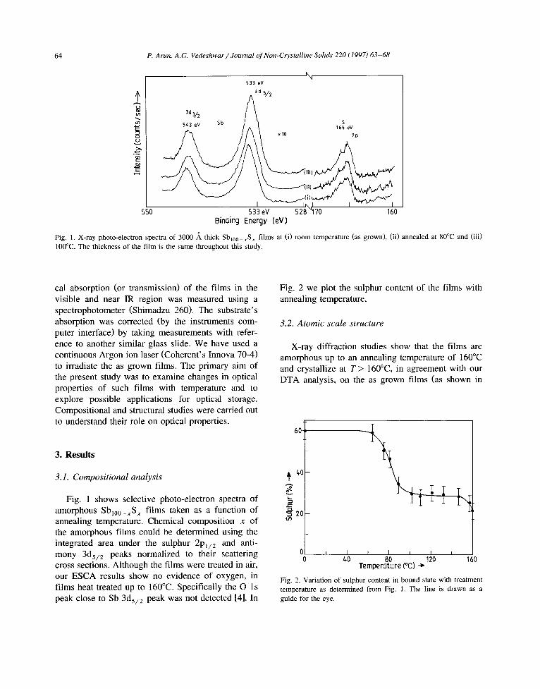
X-ray diffraction studies show that the films are amorphous up to an annealing temperature of 160°C and crystallize at T > 160°C, in agreement with our DTA analysis, on the as grown films (as shown in
60,
4C
-~ 2 0 U3
t I I [ i I i ~0 80 120 160
Temper0ture (°C) -~
Fig. 2. Variation of sulphur content in bound state with treatment temperature as determined from Fig. 1. The line is drawn as a guide for the eye.
P. Arun, A. G. Vedeshwar / Journal of Non-C~stalline Solids 220 (1997) 63-68 65
i i i i
v 0 100 200 TEMPERATURE ( °C) > >-
Z ~ ~ ~ ~
lo* 60* 2 0 - - ' -
Fig. 3. X-ray diffractogram of Sb2S 3 film annealed at 162°C along with DTA of as grown Sb2S 3 film given in inset.
2t,01 . , <
N 1601
r-~ 801
(d)
(c}
(b)
Fig. 3 along with X-ray diffractogram of Sb2S 3 film heat-treated at 162°C). Calculated radial electron density distribution (REDD) for few samples are displayed in Fig. 4. The REDD was calculated fol- lowing the standard method as described in Refs. [5,6]. Similar calculations for Sb2S 3 can be found in the literature for powders [7-9] and films [10-12]. The REDD of as grown film shown at the bottom of the figure is similar to those in the literature [12,9] except for a small first peak at 0.255 nm (shown by arrow). The first peak at 0.255 nm is the shortest distance between S b - S atoms suggesting that trigo- nal pyramidal SbS 3 units represent the basic building block of the network structure [9,12]. However, the small first peak in our case shows that the trigonal pyramids in amorphous films are disordered com- pared to powder [9], which is due to the fact that the structure of amorphous films depend on the tech- nique of preparation [1]. It should be noted that our films were grown at room temperature while those of Dalba et al. [ 12] were grown at a higher temperature
(a)
0 2 / 4 6 8 r ( A )
Fig. 4. Radial electron density distribution (REDD) for (a) as grown and heat-treated Sb2S 3 films at (b) 98°C, (c) 134°C and (d) 160°C. The first weak peak at r = 0.255 nm in (a) is shown by the
a l T O W .
(300°C) and this feature is responsible for the pro- nounced first peak observed by Dalba et al. We also observed growth of the first peak after heating the films as shown in Fig. 4. This effect supports the view that trigonal pyramid units are the elements of local structure, particularly when films are heated to 60°C or above. We have compared the position of the main peaks of our REDD with the available data
Table 1 REDD analysis of amorphous Sb 2 S 3 films. Comparison between the present work and the experimental results in the literature
Sample Position of main peaks in REDD (A) Ref.
R I R 2 R 3
Amorphous film 2.5 3.9 [ 10] Amorphous film 2.6 4.0 [11] Amorphous film 2.45 3.75 5.72 [12] As grown film 2.55 3.95 5.3 present work Treated at 98°C 2.25 3.8 5.4 present work Treated at 160°C 2.3 3.8 5.35 present work
66 P. Arun, A.G. Vedeshwar / Journal of Non-C~stalline Solids 220 (1997) 63-68
0 500
v
._~ 50
E
I--
3.0
X
'O c
"~2.5
700 900 w~velength (nm) --~
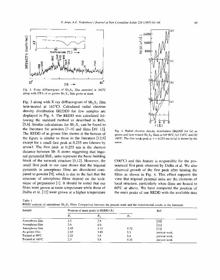
Fig. 5. Optical transmission in the visible region for (a) as grown and heat-treated Sb2S 3 films at (b) 134°C and (c) 147°C.
1.0- t ,-600 nm
z
~ 0 . 5 - o t~ m
I [ I 0 20 t~0 60
Sulphur (%)
Fig. 7. Variation of optical absorbance (at two wavelengths) of heat-treated Sb2S 3 film with sulphur content of the film. The line is drawn as a guide for the eye.
on thin films in Table 1. The radii of the first and second coordination shell, R~ and R 2, are reduced after heating at 70°C and remain unchanged at higher temperatures. Therefore, some chemical ordering is promoted at about 70°C and thereafter the structure remains the same to 162°C when crystallization oc- curs (Fig. 3).
3.3. Optical properties
Optical transmission in the visible and near IR range for three different films is displayed in Fig. 5.
2.0 I I I I I 20 t,O 60
Sulphur (%)
Fig. 6. Variation of refractive index (at 800 nm) with sulphur content of heat-treated Sb2S 3 film as determined from Fig. 5. The line is drawn as a guide for the eye.
The refractive index (n) was determined as a func- tion of wavelength by drawing a continuous curve on maxima and minima of the interference fringe pat-
100
1000
5 E BOO
~ 6 0 0
~,00
// s(%)
~-71 , /
~oO 1 I I
1.8 2.1 2./, h.V (eV)
200 I 1.5 2.7 3.0
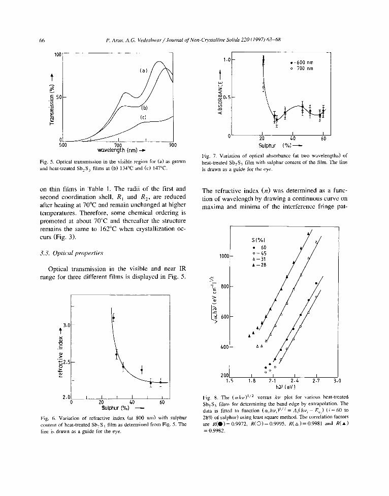
Fig. 8. The (o~hu) I/2 versus hu plot for various heat-treated Sb2S 3 films for determining the band edge by extrapolation. The data is fitted to f u n c t i o n ( o l i h P i ) 1 / 2 = Ai(hv i - Eo) (i = 60 to 28% of sulphur) using least square method. The correlation factors are R ( O ) = 0.9972, R ( O ) = 0.9995, R(z~)= 0.9981 and R(A) = 0.9982.
P. Arun, A.G. Vedeshwar / Journal of Non-Crystalline Solids 220 (1997) 63-68 67
tern of the spectra as described in Ref. [13]. We could determine n for samples annealed at tempera- tures < 135°C, since the fringe pattern decreases in amplitude at higher temperatures as illustrated in spectra (c). Fig. 6 displays n determined at 800 nm as a function of sulphur content of the films.
The variation of absorbance at two wavelengths (determined from recorded absorbance spectra) with sulphur content is shown in Fig. 7. The absorption coefficient, c~, was calculated as a function of inci- dent photon energy (hv ) , for all samples using the recorded absorbance spectra following the procedure employed in case of semiconductors near the band edge [14]. The absorption edge for amorphous mate- rials can then be determined from the relation be- tween c~ and hu given by Refs. [15,16]:
ozhv= A( h v - Eo) 2,
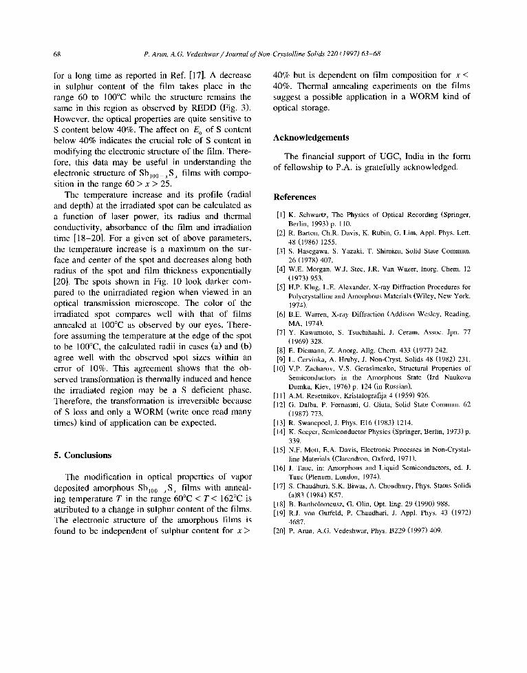
where E o is the optical energy gap or absorption edge of the material and A is a constant. Eo was determined by extrapolating the linear region of the plot between (cehv) 1/2 and hv as shown in Fig. 8.
The variation of E o with sulphur concentration of the film is shown in Fig. 9. The Eo is affected by sulphur content only for a content < 40%.
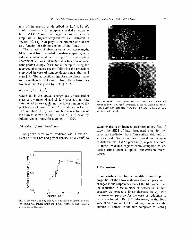
Fig. 10. SEM of laser (continuous Ar + with A= 514 nm and power density 40 W/cm 2) irradiated as grown amorphous Sb2S 3 film. Laser was irradiated from the film side in (a) and from substrate side in (b).
3.4. Effect o f laser irradiation
As grown films were irradiated with a cw Ar + laser (A = 514 nm and power density 40 W / c m 2) to
2.C >~
J
8
uJ
C)
1.0 I I I 2 0 ~0 60 Sulphur ( % ) ~
Fig. 9. The optical energy gap E o as a function of sulphur content for various heat-treated amorphous SbzS 3 films. The line is drawn as a guide for the eye.
examine the laser induced transformations. Fig. l0 shows the SEM of laser irradiated spots for two cases (a) irradiation from film surface side and (b) substrate side. We can see transformed circular spots of different radii (a) 55 Ixm and (b) 6 p~m. The color of these irradiated regions were compared to an- nealed films under a optical transmission micro- scope.
4. Discussion
We attribute the observed modifications of optical properties of the films with annealing temperature to changes in the sulphur content of the film rather than the reduction in the number of defects in the film because we expect a linear decrease in Eo with treatment temperature for the case of reduction of defects as found in Ref. [17]. Moreover, heating for a very short duration ( < 1 rain) may not reduce the number of defects in the film compared to heating
68 P. Arun, A. G. Vedeshwar / Journal of Non-Crystalline Solids 220 (1997) 63-68
for a long time as reported in Ref. [17]. A decrease in sulphur content of the film takes place in the range 60 to 100°C while the structure remains the same in this region as observed by REDD (Fig. 3). However, the optical properties are quite sensitive to S content below 40%. The affect on E o of S content below 40% indicates the crucial role of S content in modifying the electronic structure of the film. There- fore, this data may be useful in understanding the electronic structure of Sb~00_xS x films with compo- sition in the range 60 > x > 25.
The temperature increase and its profile (radial and depth) at the irradiated spot can be calculated as a function of laser power, its radius and thermal conductivity, absorbance of the film and irradiation time [18-20]. For a given set of above parameters, the temperature increase is a maximum on the sur- face and center of the spot and decreases along both radius of the spot and film thickness exponentially [20]. The spots shown in Fig. 10 look darker com- pared to the unirradiated region when viewed in an optical transmission microscope. The color of the irradiated spot compares well with that of films annealed at 100°C as observed by our eyes. There- fore assuming the temperature at the edge of the spot to be 100°C, the calculated radii in cases (a) and (b) agree well with the observed spot sizes within an error of 10%. This agreement shows that the ob- served transformation is thermally induced and hence the irradiated region may be a S deficient phase. Therefore, the transformation is irreversible because of S loss and only a WORM (write once read many times) kind of application can be expected.
5. Conclusions
The modification in optical properties of vapor deposited amorphous Sb~00 xSx films with anneal- ing temperature T in the range 60°C < T < 162°C is attributed to a change in sulphur content of the films. The electronic structure of the amorphous films is found to be independent of sulphur content for x >
40% but is dependent on film composition for x < 40%. Thermal annealing experiments on the films suggest a possible application in a WORM kind of optical storage.
Acknowledgements
The financial support of UGC, India in the form of fellowship to P.A. is gratefully acknowledged.
References
[1] K. Schwartz, The Physics of Optical Recording (Springer, Berlin, 1993)p. 110.
[2] R. Barton, Ch.R. Davis, K. Rubin, G. Lim, Appl. Phys. Lett. 48 (1986) 1255.
[3] S. Hasegawa, S. Yazaki, T. Shimizu, Solid State Commun. 26 (1978) 407.
[4] W.E. Morgan, W.J. Stec, J.R. Van Wazer, Inorg. Chem. 12 (1973) 953.
[5] H.P. Klug, L.E. Alexander, X-ray Diffraction Procedures for Polycrystalline and Amorphous Materials (Wiley, New York, 1974).
[6] B.E. Warren, X-ray Diffraction (Addison Wesley, Reading, MA, 1974).
[7] Y. Kawamoto, S. Tsuchihashi, J. Ceram. Assoc. Jpn. 77 (1969) 328.
[8] E. Diemann, Z. Anorg. Allg. Chem. 433 (1977) 242. [9] L. Cervinka, A. Hruby, J. Non-Cryst. Solids 48 (1982) 231.
[10] V.P. Zacharov, V.S. Gerasimenko, Structural Properties of Semiconductors in the Amorphous State (Izd Naukova Dumka, Kiev, 1976) p. 124 (in Russian).
[11] A.M. Resetnikov, Kristalografija 4 (1959) 926. [12] G. Dalba, P. Fornasini, G. Giuta, Solid State Commun. 62
(1987) 773. [13] R. Swanepoel, J. Phys. El6 (1983) 1214. [14] K. Seeger, Semiconductor Physics (Springer, Berlin, 1973) p.
339. [15] N.F. Mott, E.A. Davis, Electronic Processes in Non-Crystal-
line Materials (Clarendron, Oxford, 1971). [16] J. Tauc, in: Amorphous and Liquid Semiconductors, ed. J.
Tauc (Plenum, London, 1974). [17] S. Chaudhuri, S.K. Biwas, A. Choudhury, Phys. Status Solidi
(a)83 (1984) K57. [18] B. Bartholomeusz, G. Olin, Opt. Eng. 29 (1990) 988. [19] R.J. von Gutfeld, P. Chaudhari, J. Appl. Phys. 43 (1972)
4687. [20] P. Arun, A.G. Vedeshwar, Phys. B229 (1997) 409.