Embed Size (px)
Citation preview

E / EEPRE / EEPROMsOMs
We may be approaching the time when it’s appropriate to say “stand back, here
comes FLASH.” We saw two 32Mbit devices and both include examples of very
up-to-date technology, including the 0.25 micron gates on the Toshiba device.
Also, the two-bit per cell capability seems to be getting very near! There just
seems to be no way this product type can be excluded from any new technology
developments. Almost everything developed for any other class of products
should be useable by FLASH. Even the UVEPROMs are at the 0.5 micron gate
length stage now.
Integrated Circuit Engineering Corporation
3-1

Die size
Min. M1 width/space
Min contact (Met. to Si)
Min. Poly 3
Min. Poly 2
Min. Poly 1
Min. gate-(N)†
Min. gate-(P)†
Cell pitch
Cell area
AMDAM27C010-200DC1Mb (x8) UVEPROM 9634
3.7 x 4.3mm(15.9mm2)
1.2µm/1.1µm
1.0µm+
NA
0.7µm*
0.7µm
0.7µm
0.8µm
2.3µm x 2.4µm
5.5µm2
SGS-THOMSONM27C1001-15F1 1Mb (x8) UVEPROM 9514
3.4 x 3.4mm(11.5mm2)
1.3µm/1.0µm
0.7µm+
NA
0.5µm*
0.5µm
0.5µm
0.5µm
1.8µm x 1.95µm
3.5µm2
SANDISK34MbFlash EEPROM1996
9.1 x 13.3mm(121mm2)
0.75µm/0.9µm
0.8µm+
1.0µm
0.35µm
0.6µm
1.0µm
1.0µm
1.1µm x 1.6µm
1.8µm2
TOSHIBATC5832FT 32Mb (x8)NAND EEPROM 9528
14.7 x 7mm(103mm2)
0.7µm/0.6µm
1.0µm
0.5µm*
0.25µm
0.25µm
0.25µm
0.6µm
0.85µm x 1.5µm
1.3µm2
HORIZONTAL DIMENSIONS (DESIGN RULES)
* Polycide † Physical gate length� + Plugs
E/EEPROMs
Table 3-1
Integrated Circuit E
ngineering Corporation

Final passivation
Metal 1
Pre-metal dielectric
Poly 3
Poly 2
Poly 1
Recessed oxide
N-well
P-well
Epi
* Polycide� ❶ Could not delineate� ❷ Non-recessed
VERTICAL DIMENSIONS
0.6µm
1.0µm
0.6µm
NA
0.3µm*
0.15µm
0.4µm
4.5µm
?❶
None
AMDAM27C010-200DC1Mb (x8) UVEPROM 9634
0.75µm
0.75µm
0.5µm
NA
0.5µm*
0.15µm
0.45µm
4.5µm
?❶
None
SGS-THOMSONM27C1001-15F1 1Mb (x8) UVEPROM 9514
0.45µm
0.8µm
0.5µm
0.2µm
0.3µm
0.25µm
0.45µm❷
3µm
?❶
8µm
SANDISK34MbFlash EEPROM1996
1µm
0.9µm
1.1µm
0.3µm*
0.2µm
0.15µm
0.4µm
3.0µm
10µm
None
TOSHIBATC5832FT 32Mb (x8)NAND EEPROM 9528
E/EEPROMs
Table 3-2
Integrated Circuit E
ngineering Corporation

Final passivation
Metal 1
Plugs
Reflow glass
Polycide metal
DIE MATERIALS
glass
Titanium-NitrideAluminumTitanium
Tungsten
BPSG
Tungsten
AMDAM27C010-200DC1Mb (x8) UVEPROM 9634
glass
Titanium-NitrideAluminumTitanium-NitrideTitanium
Tungsten
BPSG
Tungsten
SGS-THOMSONM27C1001-15F1 1Mb (x8) UVEPROM 9514
Nitride
Titanium-NitrideAluminum
Tungsten
BPSG
NA
SANDISK34MbFlash EEPROM1996
undoped glass
Titanium-NitrideAluminum
NA
BPSG + TEOS(?)
Tungsten
TOSHIBATC5832FT 32Mb (x8)NAND EEPROM 9528
E/EEPROMs
Table 3-3
Integrated Circuit E
ngineering Corporation

TECHNOLOGY DESCRIPTIONTECHNOLOGY DESCRIPTION
SANDISK34Mbit CMOS FLASH EEPROM
Intr oduction Ref. report SCA 9611-471
These dice were obtained from a 15 CF (“COMPACTFLASH”) Flash card. One 15Mbyte and
one 10Mbyte FLASHCARD was received for the analysis. The dice analyzed were 34Mbit
devices. No information on speed, organization or power requirements was available. It is
believed that dice were fabbed early in 1996.
See tables for specific dimensions and materials identification and see figures for examples of
physical structures.
Impor tant/Unique Featur es
– Non-recessed field oxide isolation.
– Tungsten plugs used at all contacts.
– Three poly unique Flash EEPROM cell design.
Quality
Quality of the process implementation was good. We found no items of serious concern.
In the area of layer patterning, etch definition and control were both good.
Alignment and registration were also good.
Technology
These devices were manufactured by a non-recessed field oxide, CMOS (possibly twin-well)
process in a P-epi on a P substrate. One level of metal and three levels of poly were present.
Passivation consisted of a thick layer of nitride and was not planarized.
Integrated Circuit Engineering CorporationSanDisk
3-2

The single level of metal was defined by a standard dry-etch technique. Metal consisted of alu-
minum with a titanium-nitride cap (no barrier was visible).
Tungsten plugs were used for all vertical interconnect. Plugs appeared to be lined (underneath
only) with titanium-nitride liners.
Pre-metal dielectric was a single layer of reflow glass (BPSG) over various densified oxides.
This layer was reflowed prior to contact cuts,and provided the only planarization. No SOG
was used anywhere in the process.
Three layers of poly (no silicide) were used in the cell array. It is probable that poly 3 is also
used to form all standard gates on the die; however, it was impossible to positively identify the
gate poly as poly 3, and it is possible that gates are made with a fourth level of poly.
Oxide sidewall spacers were present and were left in place, but an LDD process was not used
(according to Sandisk). Apparently, standard source/drain diffusions were implanted in periph-
eral circuits,but a separate non-self-aligned diffusion formed the sources/drains in the memory
cells.
Direct poly to diffusion (buried) contacts were not used.
Field oxide isolation consisted of a non-recessed (deposited and densified) oxide that was well
implemented. A step in this oxide was present at well boundaries but no sign of the presence of
twin-wells was found. An epi layer was present.
Redundancy fuses were not present.
Memory Cell Structures
The Flash cell design employed three levels of poly, a non self-aligned bit line diffusion,and no
nitrides for the thin dielectrics. It was noted that the thick non-recessed field oxide provides for
minimum spacing between the poly 1 elements. It should be mentioned that although peripher-
al gates measured only 1 micron in length (not very aggressive), the memory array uses 0.35
micron wide poly 2 lines and 0.6 x 0.9 micron poly 1 pads with 0.4 micron spacing. The EEP-
ROM cell size was 1.8 microns2.
Overall minimum feature size measured anywhere on these dice was the 0.35 micron (poly 2 in
cell).
Integrated Circuit Engineering CorporationSanDisk
3-3

Packaging/Assembly
As mentioned, these EEPROM dice were obtained from a 15 CF (“COMPACTFLASH”) Flash
card.
The 15Mbyte FLASHCARD employed five dice (one controller die and four 34Mbit Flash
EEPROM dice) mounted on printed circuit boards along with various surface mount devices.
All EEPROM dice were embedded in an epoxy encapsulant. The controller die was packaged
in a standard 100-pin Plastic Quad Flat Pack (PQFP) and mounted on the PC board.
The standard thermosonic wirebonds on the die were made to pads on the die that had a pitch of
250 microns with 140 micron spacing and all placed along one edge of the die. Pads were 110
microns wide with a 100 micron windows.
No die coat was present.
Integrated Circuit Engineering CorporationSanDisk
3-4

Integrated Circuit Engineering CorporationSanDisk
Optical photographs of the SanDisk 15M Compactflash Flash Card.
ADAPTER
FLASH CARD
DAUGHTERBOARD
1144
4422
4444
3311
4444
2244
4433
MOTHERBOARD
CONTROLLER
4 MEG EEPROM
Mag. 1x
Mag. 2.2x
Mag. 2.2x

Integrated Circuit Engineering CorporationSanDisk
Whole die photograph of the SanDisk 505032A 34Mbit EEPROM. Mag. 17x.

Mag. 5000x,60°
Mag. 10,000x
SEM section views of general construction.
Integrated Circuit Engineering CorporationSanDisk
METAL
FIELD OXIDE
WPLUG
POLY GATE
N+ S/D
DIFFUSION
POLY GATE
POLY ON FIELD OXIDE

Mag. 20,000x,45°
parallel to bit line,Mag. 13,000x
perpendicular to bit line,Mag. 13,000x
Integrated Circuit Engineering CorporationSanDisk
Perspective and section views of the Flash EEPROM cells.
METAL BIT LINE
POLY 3
POLY 2
POLY 1
WPLUG
DIFFUSED BIT LINE
POLY 3 POLY 2
POLY 1
POLY 3 CONTROL LINE
POLY 2 WORD LINE
POLY 1 FLOATING GATE
DIFFUSED BIT LINES

TECHNOLOGY DESCRIPTIONTECHNOLOGY DESCRIPTION
TOSHIBA TC5832FT32Mbit CMOS NAND EEPROM
Intr oduction Ref. report SCA9604-458
These parts were packaged in 44-pin format (40 pin) plastic Thin Small Outline Packages
(TSOPs). They were engineering samples (marked ES). They are organized in a 528 x 8K x 8
array (528 byte page),offer a 10nsec. maximum access time and operate from a single 5V
power source. They were date coded 9528 (week 28 of 1995).
See tables for specific dimensions and materials identification and see figures for examples of
physical structures.
Impor tant/Unique Featur es
– Single metal,three poly, twin/nested well CMOS process.
– Shallow extended source/drains.
– Use of at least three different gate oxides plus the interpoly dielectric.
– Smallest cell size seen in 1996!
Quality
Quality of the process implementation was good, except at metal contacts where aluminum
thinning greater than 95 percent was noted. These devices would really benefit from a tungsten
plug addition.
In the area of layer patterning, etch definition and control were both good.
Alignment and registration were also good.
Technology
The devices were manufactured by a twin (multiple)-well, selective oxidation CMOS process
employing an N-substrate (no epi), one level of metal,and three levels of poly.
Integrated Circuit Engineering CorporationToshiba TC5832
3-5

Passivation consisted of two layers of undoped glass,which varied greatly in thickness due to
the large metal steps.
They incorporated a single level of metal defined by a standard dry-etch technique. Metal con-
sisted of aluminum with a titanium-nitride barrier (no cap was visible). It should be noted that
poly 3 (tungsten polycide) functioned as a metal interconnect also.
Standard contacts were employed throughout (no plugs),and represent a feature hopefully elim-
inated in the full production devices.
Pre-metal dielectric 2 (between metal and poly 3) appeared to be a layer of BPSG reflow glass
used for planarization. A first thick layer of BPSG reflow glass (pre-metal dielectric 1) was
used for planarization under poly 3. No spin-on-glass (SOG) was used anywhere.
Three levels of polysilicon were used. Polycide 3 (poly and tungsten silicide) was used as a
metal substitute in both the array and peripheral circuit areas. Poly 2 formed all gates for the
peripheral circuits and the word (control) lines in the cell array. Poly 1 was employed only in
the cell array (for all floating gates). A separate (third) gate oxide was used under all poly 2
gates in the periphery.
Sidewall spacers had been used throughout and removed.
Implanted source/drain diffusions included shallow LLD extensions plus deep diffusions at
metal contacts. Diffusions were not silicided.
Direct poly to diffusion contacts (buried contacts) were used only in the cell array for the poly-
cide (poly 3) bit line contacts.
Standard recessed field oxide isolation (LOCOS) was used and was well implemented. A step
was present at the top of the LOCOS only.
Redundancy fuses were not present.
Memory Cell Structures
The EEPROM array used the standard dual gate stacked cell implemented in a NAND configu-
ration. Separate program lines were present at the edge of each end of the 16-bit string (for
“Flash” programming?). These program gates used a continuous poly 1 line under the poly 2, a
different gate oxide under the poly 1, the same ONO between poly 1 and 2,and wider poly 1
Integrated Circuit Engineering CorporationToshiba TC5832
3-6

and 2 (gate length) than the memory gates. Polycide (poly 3) was used for all bit lines. The
memory cell gates themselves are arranged in strings of 16 cells,use a different gate oxide than
either the control cells or the peripheral circuit gates,use an ONO between poly 1 and poly 2
and are the shortest gates anywhere on the dice. The EEPROM cell size was 1.3 micron2, by
far the smallest cell size we’ve ever seen. However, this dimension does not include the over-
head due to the special control lines,etc. But, if the array is measured and divided by the num-
ber of memory bits, the cell size is 1.68 micron2 - still the smallest cell size seen in 1996!
Overall minimum feature size measured anywhere on these dice was the 0.25 micron poly 1 and
2 (gates in cell).
Packaging/Assembly
As mentioned, these parts were packaged in 44-pin format (40 pin) plastic Thin Small Outline
Packages (TSOPs) date coded 9528. They used a hollow center leadframe paddle, silver epoxy
die attach, and standard thermosonic wirebonding employing gold wire.
Wirebond pads on the die had a minimum pitch of 665 microns with 550 micron spacing. Pads
were 115 microns wide with a 105 micron windows.
No die coat was present.
Integrated Circuit Engineering CorporationToshiba TC5832
3-7
Integrated Circuit Engineering CorporationToshiba TC5832
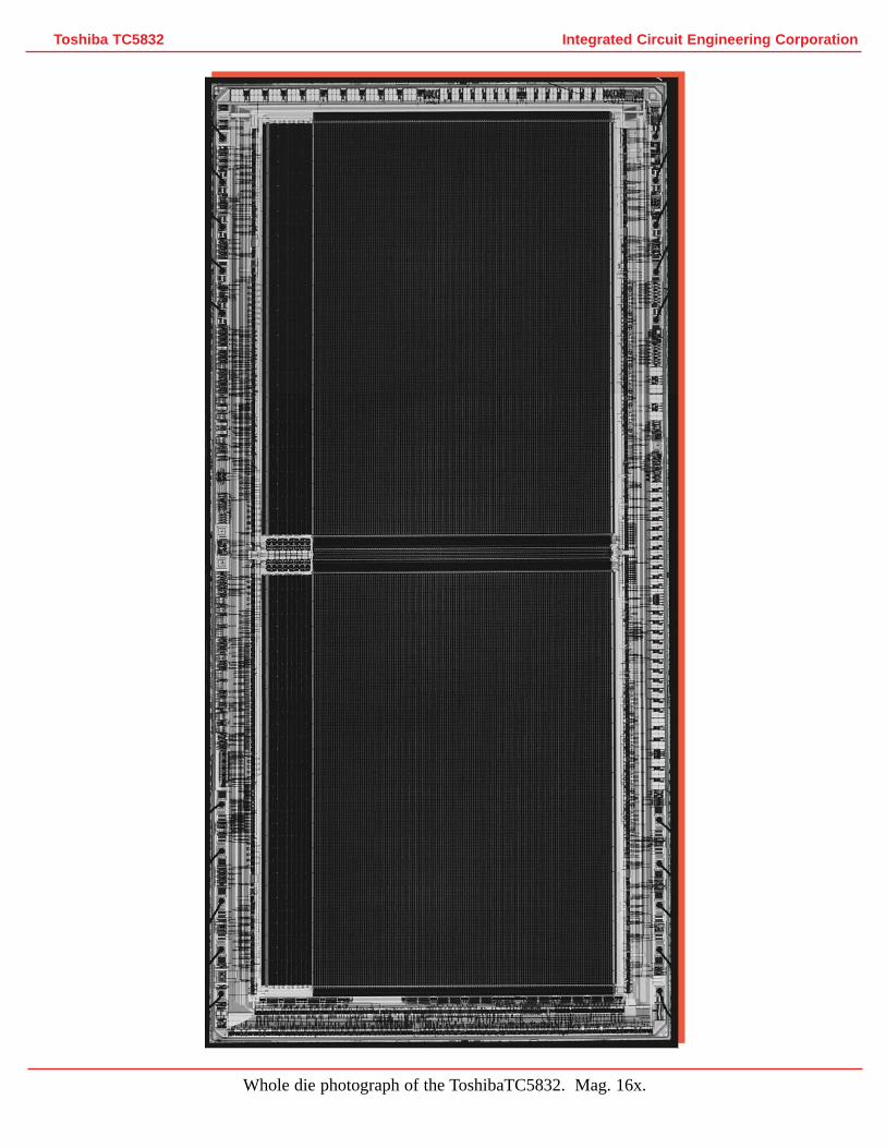
Whole die photograph of the ToshibaTC5832. Mag. 16x.

Mag. 8400x
Mag. 4000x,60°
Mag. 35,000x
Integrated Circuit Engineering CorporationToshiba TC5832
SEM views of the general die structures.
METAL
POLY 3
POLY 2 GATE
N+ DIFFUSION
POLY 2GATE
N+
POLY 3
POLYOXIDE

SEM views of memory cells in section.
Mag. 31,000x
Mag. 11,000x
Integrated Circuit E
ngineering Corporation
Toshiba TC
5832
METALPOLY 3
POLY 2
EMBEDDINGCOMPOUND
EDGE CELLS POLY 1
POLY 3
EDGE CELL
POLY 2
POLY 1
N+
N+
DIFFERENTGATE OXIDE
EDGE CELLS

TECHNOLOGY DESCRIPTIONTECHNOLOGY DESCRIPTION
SGS-THOMSON M17C1001-15F1 1Mbit CMOS UVEPROM
Intr oduction Ref. report SCA 9612-518
The parts were packaged in 32-pin Ceramic Dual In-Line Packages (CERDIPs) with a quartz
window. These were fully functional production devices organized in a 128K x 8 design. They
offer a fast access time of 45 nsec., a low power standby mode, electronic signature, operate
from a 5V power source but require a 12.75V programming voltage. They were date coded
9514 (week 14 of 1995).
See tables for specific dimensions and materials identification and see figures for examples of
physical structures.
Impor tant/Unique Featur es
– Unusual metal interconnect.
– Aggressive design rules (0.5 micron gates).
Quality
Quality of the process implementation was very good. We found no areas of concern.
In the area of layer patterning, etch definition and control were both good.
Alignment and registration were also good.
Technology
These devices were manufactured by a twin-well, selective oxidation CMOS process on a P
substrate (no epi). A single level of metal and two levels of poly were used.
Passivation consisted of two layers of silicon-dioxide and was not planarized.
Integrated Circuit Engineering CorporationSGS M27C1001
3-8

They incorporated a single level of metal defined by standard dry-etch techniques. Metal con-
sisted of aluminum with a titanium-nitride cap and titanium over titanium-nitride on titanium
barrier. The presence of the titanium layer over the titanium-nitride barrier is unique. This
layer is deposited after plug formation thus covering the tops of the plugs which normally is
done with a titanium-nitride.
Tungsten plugs were used at all contacts,and were lined underneath with titanium-nitride.
Pre-metal dielectric was a single layer of reflow glass (BPSG) over densified oxides. This layer
was reflowed prior to contact cuts,and it provides the only planarization as no SOG was used
anywhere in this process.
Two levels of polysilicon were used. Poly 2 (tungsten silicide) was used to form all gates on
the die and the select/word lines in the EPROM cell array. All gates in the periphery used oxide
sidewall spaces that were left in place. Poly 1 (no silicide) was used exclusively in the memory
cells to form the floating gates.
Standard implanted source/drain diffusions were used in the peripheral circuits and they includ-
ed an LDD process. Salicide was not used. Other implants were present in the memory array
(see below).
The process appears to use three different thin oxide dielectrics. One for gate oxide in peripher-
al circuits,one for gate oxide in the memory array and one for the interpoly in the array.
Interpoly or buried contacts were not used, nor was any other special interconnect such as a
local interconnect.
Standard LOCOS isolation was employed and well implemented. A step was present confirm-
ing the presence of twin-wells.
Redundancy fuses were not present.
Memory Cell Structures
Memory cells consisted of a standard dual gate stacked poly EPROM design. Metal was used
for the bit lines. Poly 2 was used to form the word/select lines,and poly 1 was used exclusively
to form the floating gates. As mentioned, oxide was used as the interpoly dielectric. The gates
used for the memory cells were very small,measuring 0.5 micron long and only 0.4 micron
wide. The EPROM cell size was 3.5 microns2, which is the smallest cell size we’ve seen for a
Integrated Circuit Engineering CorporationSGS M27C1001
3-9
UVEPROM cell. Sidewall spacers were left only on the bit contact side of the memory cell
gates where they appear to have provided the masking for the deep contact diffusions.
Overall minimum feature size measured anywhere on these dice was the 0.5 micron gates in the
cell array.
Packaging/Assembly
As mentioned, the parts were packaged in 32-pin Ceramic Dual In-Line Packages (CERDIPs)
with quartz windows. Aluminum ultrasonic wirebonds were employed.
The die was mounted to the cavity f loor with silver-filled glass die attach. Wirebond pads on
the die had a pitch of 170 microns with 30 micron spacing. Pads were 140 microns wide with
130 micron windows.
Integrated Circuit Engineering CorporationSGS M27C1001
3-10

Integrated Circuit Engineering CorporationSGS M27C1001
Whole die photograph of the SGS M27C1001. Mag. 50x.
PIN 1

Mag. 10,000x
Mag. 2800x,60°
Mag. 40,000x
Integrated Circuit Engineering CorporationSGS M27C1001
SEM section and perspective views of general structure.
PASSIVATION
METAL
N+ DIFFUSION P+ S/D P+ S/D
PRE-METALDIELECTRIC
POLY 2
POLY 2
PRE-METAL DIELECTRIC
SILICIDE
POLY 2
GATE OXIDE
N+ S/DN+ S/D

SEM section views of the memory cell array. Mag. 13,000x.
Integrated Circuit Engineering CorporationSGS M27C1001
PASSIVATION
METAL BIT LINE
WPLUG
N+ S/D
POLY 1 FLOATING GATE
POLY 2 WORD/SELECT
PASSIVATION
METALPOLY 2 WORD/SELECT
POLY 1 FLOATING GATE

TECHNOLOGY DESCRIPTIONTECHNOLOGY DESCRIPTION
AMD AM27C0101Mbit CMOS UVEPROM
Intr oduction Ref. report SCA 9612-517
The parts were packaged in 32-pin Ceramic Dual In-Line Packages (CERDIPs) with quartz
windows. These were fully functional production devices organized in a 128K x 8 design.
They offer a fast access time (55 nsec),a static standby mode and operate from a 5V power
source but require a 12.75V programming voltage. They were coded 9634 (week 34 of 1996).
See tables for specific dimensions and materials identification and see figures for examples of
physical structures.
Unusual/Unique Featur es
– Twin-well CMOS with tungsten plugs.
– Sub-micron gate lengths (0.7 micron).
– ONO dielectric used in array cells.
Quality
Quality of the process implementation was very good. We found no areas of concern.
In the area of layer patterning, etch definition and control were both good.
Alignment and registration were also good.
Technology
These devices were manufactured by a twin-well, selective oxidation CMOS process on a P
substrate (no epi). A single level of metal was used and two levels of poly.
Passivation consisted of two layers of silicon-dioxide and was not planarized (a method AMD
has used on some products of this type).
Integrated Circuit Engineering CorporationAMD AM27C010
3-11

They incorporated a single level of metal defined by a standard dry-etch technique. The metal
consisted of aluminum with a titanium-nitride barrier. A thin titanium adhesion layer was used
under the barrier.
Tungsten plugs were used for all vertical interconnect and they were lined with titanium-nitride
liners underneath only (i.e., titanium-nitride deposition before tungsten deposition only).
Pre-metal dielectric was a single layer of reflow glass (BPSG) over densified oxides. This layer
was reflowed (prior to contact cuts) to provide the only planarization present. No SOG was
used anywhere in this process.
Two levels of polysilicon were used. Poly 2 (tungsten silicide) was used to form all gates on the
die and the select/word lines in the EPROM cell array. All gates in the peripheral circuitry used
oxide sidewall spacers that were left in place. Poly 1 (no silicide) was used exclusively in the
memory cells to form the floating gates.
Standard implanted source/drain diffusions were used in the peripheral circuits and they includ-
ed oxide sidewall spacers that were left in place, and an LDD process. Salicide was not used.
Interpoly or buried contacts were not used, nor was any special contact layers such as a local
interconnect.
At least three thin oxide dielectrics were used. One under poly 1 in the memory array, one
under all gates in the peripheral circuits,and the interpoly (ONO) layer in the array.
Standard LOCOS isolation was employed and well implemented. A step was present,confirm-
ing the presence of twin-wells.
Redundancy fuses were not present.
Memory Cell Structures
Memory cells consisted of a standard dual gate stacked EPROM design. Metal was used for the
bit lines. Poly 2 was used to form the word/select lines,and poly 1 was used
exclusively to form the floating gates. An oxide-nitride-oxide (ONO) was used as the interpoly
dielectric. The EPROM cell size was 5.5 microns2. This is surprisingly large for a mid-1996
timeframe technology.
Integrated Circuit Engineering CorporationAMD AM27C010
3-12

Overall minimum feature size measured anywhere on these dice was the 0.7 micron poly 1 and
poly 2 (memory cell gates).
Packaging/Assembly
As mentioned, the parts were packaged in 32-pin Ceramic Dual In-Line Packages
(CERDIPs) with quartz windows. Aluminum ultrasonic wirebonds were employed.
The die was mounted to the cavity f loor with silver-filled glass die attach. Wirebond pads on
the die had a pitch of 230 microns with 90 micron spacing. Pads were 140 microns wide with
120 micron windows.
Integrated Circuit Engineering CorporationAMD AM27C010
3-13

Integrated Circuit Engineering CorporationAMD AM27C010
Whole die photograph of the AMD AM27C010. Mag. 40x.
PIN 1

Mag. 10,000x
Mag. 4600x
Mag. 52,000x
Integrated Circuit Engineering CorporationAMD AM27C010
SEM views of general structures.
PRE-METALDIELECTRIC
POLY 2METAL
PASSIVATION
N+ S/D
POLY 2
DIFFUSION
PRE-METAL DIELECTRIC
SILICIDE
POLY 2
N+ S/D N+ S/DGATE OXIDE

Mag. 52,000x,60°
Mag. 13,000x
Mag. 52,000x,60°
Integrated Circuit Engineering CorporationAMD AM27C010
Perspective and section SEM views of the EPROM cells.
METAL BIT LINE
POLY 2
POLY 1W PLUG
N+ S/D
POLY 2 WORD/SELECT LINE
ONO DIELECTRIC
POLY 1 FLOATING GATE
NITRIDEW SILICIDE
POLY 2
POLY 1