Embed Size (px)
Citation preview
Cloud FPGA
EENG 428ENAS 968
bit.ly/cloudfpga

Share:bit.ly/cloudfpga
EENG 428 / ENAS 968 – Cloud FPGA© Jakub Szefer, Fall 2019 2
Lecture: Verilog – A Tutorial Introduction
Prof. Jakub SzeferDept. of Electrical Engineering, Yale University
EENG 428 / ENAS 968Cloud FPGA

Share:bit.ly/cloudfpga
Verilog – A Tutorial Introduction
This lecture is mostly based on contents of Chapter 1, from “The Verilog Hardware Description Language” book [1], 5th edition. Example figures and(modified) code are from the textbook unless otherwise specified.
Topics covered:• Very short history of Verilog• Structural and behavioral description• Combinatorial circuit description• Sequential circuit description• Module hierarchy• Seven segment module and testbench examples • Very short intro to iverilog and gtkwave open-source tools• Running iverilog and gtkwave in virtual machine
EENG 428 / ENAS 968 – Cloud FPGA© Jakub Szefer, Fall 2019 3

Share:bit.ly/cloudfpga
Verilog History
Verilog is a hardware description language (HDL) used to describe and model electronic systems built using digital logic
• Can be used to do some analog and mixed-signal designs• Originally developed only for description and simulation of circuits• Latter features were added to allow synthesis of the design into hardware
Verilog standards:• IEEE Standard 1364-1995 – initial Verilog• IEEE Standard 1364-2001 – standard used in the textbook• IEEE Standard 1364-2005 – minor updatesSystemVerilog standards:• IEEE Standard 1800-2005 – initial SystemVerilog• IEEE Standard 1800-2009 – merge SystemVerilog and Verilog into one standard• IEEE Standard 1800-2012 – minor updates• IEEE Standard 1800-2017 – current SystemVerilog
• Verilog is now subset of SystemVerilog
EENG 428 / ENAS 968 – Cloud FPGA© Jakub Szefer, Fall 2019 4

Share:bit.ly/cloudfpga
EENG 428 / ENAS 968 – Cloud FPGA© Jakub Szefer, Fall 2019 5
Verilog – A Tutorial Introduction

Share:bit.ly/cloudfpga
Structural Description of a Module
In Verilog modules are described using the module keyword and include description of inputs and outputs (not shown in this example), wires, registers, sub-modules, and any combinatorial or sequential logic
EENG 428 / ENAS 968 – Cloud FPGA© Jakub Szefer, Fall 2019 6
Module definition
Nets (wires) and registers in the module
Sub-module, instance of
built-in NAND gate
Output, and inputs to a gate
End of module definition
Specify delay of this gate

Share:bit.ly/cloudfpga
Verilog Built-In Primitive Gates and Operators
Operators:• Verilog-2001 standard supports many logical
and arithmetic operators• E.g. unary operators: +, -, !, ~, &, ~&, |, ~|, ^, ~^, ^~ • E.g binary operators: +, -, *, /, %, ==, !=, ===, !==, and more
Primitive gates:• Verilog-2001 standard supports a number of primitive gates
(these do not need to be built from logic operators):• E.g. n-input gates: and, nand, or, nor, xor, xnor
IP (Intellectual Property) cores:• Most tools and vendors provide IP cores which realize many common types of operations
• PCIe controller, DRAM controller, AXI bus controller, FIFOs, memories, etc.• Depend on the tools, vendor, and may be specific to one FPGA chip or board type• Can be used to more quickly build a design• Can create your own IP core
EENG 428 / ENAS 968 – Cloud FPGA© Jakub Szefer, Fall 2019 7
See Appendix G of the textbook for full formal
specification of the language, built-in gates, and operators
Structural description is built using the primitive gates, operators, and modules or submodules made of these
Share:bit.ly/cloudfpga
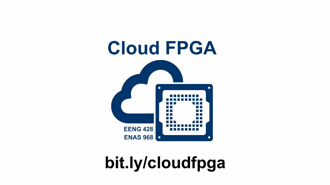
Simulating a Module
Operation of a module can be examined by creating a simulation that• Provides stimuli to the module being tested• Can capture the outputs (or any changes in the
internal state)
Simulation using a dedicated module:• Can create a Verilog module that provides stimuli to
the design under test• Use initial statements to assign
values to registers• Use $monitor statement to print
outputs (values of registers or wires)
EENG 428 / ENAS 968 – Cloud FPGA© Jakub Szefer, Fall 2019 8
Print output when any of the monitored
variables changes
Update values of registers after
specified time delay
Explicitly finish simulation, otherwise runs until no more
signals change
DUT would typically be an instance of a
module

Share:bit.ly/cloudfpga
Simulation Output and Waveforms
Simulation will typically have two types of output:• Text printed to terminal• A waveform which shows how the digital signals change in time
• Actually a waveform file, which can be viewed using a waveform viewer program
Terminal output:• Use $monitor statements
to generate output
Waveform output:• Use $dumpfile statements
to write signal values to dump file
EENG 428 / ENAS 968 – Cloud FPGA© Jakub Szefer, Fall 2019 9
Current time in simulation
Text and values to print when there is
signal change
Values to monitor for signal change
File where to dump data
Module for which to dump signals (includes any sub-
modules

Share:bit.ly/cloudfpga
Simulation Output and Waveforms
Testbench output is simply statements printed to the terminal• Example output for the seven segment decoder
Waveforms are the time-changing values of the signals• Example waveform for the seven segment decoder
EENG 428 / ENAS 968 – Cloud FPGA© Jakub Szefer, Fall 2019 10
Share:bit.ly/cloudfpga
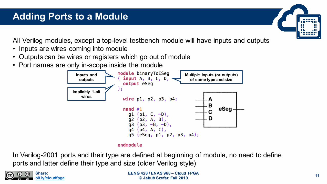
Adding Ports to a Module
All Verilog modules, except a top-level testbench module will have inputs and outputs• Inputs are wires coming into module• Outputs can be wires or registers which go out of module• Port names are only in-scope inside the module
In Verilog-2001 ports and their type are defined at beginning of module, no need to define ports and latter define their type and size (older Verilog style)
EENG 428 / ENAS 968 – Cloud FPGA© Jakub Szefer, Fall 2019 11
Inputs and outputs
Implicitly 1-bit wires
Multiple inputs (or outputs) of same type and size

Share:bit.ly/cloudfpga
Creating a Testbench for a Module
Simulation of a module (or multiple modules) can be organized using a testbench• Testbench is a top-level module• Drive inputs to design under test (DUT)
submodule or submodules• Capture output of the submodule
• Can also monitor internal submodule state
Testbench approach separates the testing from the module being tested• Goal is to test module that will be synthesized into hardware (FPGA or ASIC)• Don’t modify design under test module• Only give inputs and observer the outputs
EENG 428 / ENAS 968 – Cloud FPGA© Jakub Szefer, Fall 2019 12

Share:bit.ly/cloudfpga
Creating a Testbench for a Module
Example testbench for seven segment driver
• To-level module is the testbench• It has no inputs or outputs• Connects DUT to the tester• Tester module also outputs
print statements to terminal
EENG 428 / ENAS 968 – Cloud FPGA© Jakub Szefer, Fall 2019 13

Share:bit.ly/cloudfpga
Behavioral Modeling of Combinatorial Circuits
In a combinatorial circuit there is no “memory” as output depends on• Output only depends on current inputs• No “memory” in the circuit
Rules for combinatorialcircuits code• Make sure all inputs are in the
sensitivity list @(…)• Can use @(*) as short hand
• Make sure all possible executionsof the always block assigna value to the output
EENG 428 / ENAS 968 – Cloud FPGA© Jakub Szefer, Fall 2019 14
Module definition
Always block with sensitivity
list
“Default” assignment of
signal
Update signal value if any of the conditions
are true
eSeg is defined as regbecause it is used on the left-hand-side in always
block; but it is still combinatorial logic
Behavioral description can be synthesized to
hardware, usually

Share:bit.ly/cloudfpga
Behavioral Modeling of Sequential Circuits
Sequential circuits have “memory” and output depends on:• Current inputs• And state of the circuit
• State is stored in flip-flops• Represented by reg in Verilog• Typically D flip-flops
EENG 428 / ENAS 968 – Cloud FPGA© Jakub Szefer, Fall 2019 15
Combinatorial logic, also called next-state logic
Flip-flops storing the state of the circuit Behavioral
model of the fsm

Share:bit.ly/cloudfpga
Behavioral Modeling of Sequential Circuits
Rules for sequential code for always blocks implementing the state registers• Sensitivity list of always block for updating flip-flops only includes edges of clock, reset,
and set signals• In always block always specify reset and set conditions first
• This will give you asynchronous reset or set, that does not depend on the clock• Clock generator module can itself use reset, so usually want to be independent of the clock
• All signals on the left-hand-side need to be registers• Use non-blocking <= operator to perform all assignments in parallel
• If blocking = is used, latches may be synthesized
• Break up the state machine into the combinatorial logic and sequential logic• Can have combinatorial logic in the always block, but it will be evaluated only on clock edge
EENG 428 / ENAS 968 – Cloud FPGA© Jakub Szefer, Fall 2019 16
Share:bit.ly/cloudfpga
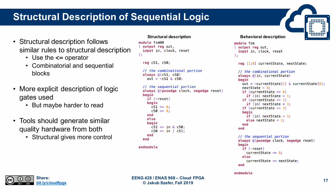
Structural Description of Sequential Logic
• Structural description followssimilar rules to structural description
• Use the <= operator• Combinatorial and sequential
blocks
• More explicit description of logicgates used
• But maybe harder to read
• Tools should generate similarquality hardware from both
• Structural gives more control
EENG 428 / ENAS 968 – Cloud FPGA© Jakub Szefer, Fall 2019 17
Structural description Behavioral description

Share:bit.ly/cloudfpga
Module Hierarchy
All hardware designs are done in hierarchical manner• Develop modules for specific tasks• Interconnect multiple modules together• Can have nesting of modules
Advantages• Easier to organize the design (and code)• Can update one module without having to update
whole design• Assuming interface inputs and outputs stay same• Often use standard interfaces such as AXI for
compatibility with other designs• Treat modules as black-boxes
• E.g. IP cores purchased• Have different versions of each module (for initial simulation vs. final design)
EENG 428 / ENAS 968 – Cloud FPGA© Jakub Szefer, Fall 2019 18
Textbook example of display driverwith clock and counter

Share:bit.ly/cloudfpga
Module Hierarchy Example
EENG 428 / ENAS 968 – Cloud FPGA© Jakub Szefer, Fall 2019 19
Textbook example of display driverwith clock and counter

Share:bit.ly/cloudfpga
EENG 428 / ENAS 968 – Cloud FPGA© Jakub Szefer, Fall 2019 20
Open-Source Verilog Tools

Share:bit.ly/cloudfpga
Icarus Verilog
Icarus Verilog, also called iverilog, is a free and open-source compiler and simulator for Verilog designs
Typical use of Icarus Verilog:• Compile a design, typically a testbench, into an assembly-like language• Run the assembly-like langauge using the vpp command
• Print statements on termain to see progress of simulation, signal values, etc.• Optionally output a waveform, which can be viewed by gtkwave or other
waveform viewer• Can also generate a netlist
• There is null target as well, useful for syntax checking
As of 2019, the latest version is 10.2 • Supports Verilog standards 1364-1995, 1364-2001, and 1364-2005• Some subset of SystemVerilog from 1800-2005, 1800-2009, 1800-2012• Does not seem to support latest 1800-2017
EENG 428 / ENAS 968 – Cloud FPGA© Jakub Szefer, Fall 2019 21
Icarus Verilog logo from:https://en.wikipedia.org/wiki/Icarus_Verilog
Share:bit.ly/cloudfpga
GTKWave
GTKWave, also called gtkwave, is a waveform viewer
• Visualize time-changing digital signals• Support different input file types, including VCD
• Value Change Dump (VCD) is ASCII-based format for dump files generated by electronic design automaton (EDA) tools
Typical use of GKTWave:• Generate a dumpfile using EDA tools
• Usually part of testbench is to dump the waveform files• Run the viewer to observe signal changes in time• Use waveform to help debug the design
• Waveforms are useful for design-time debugging• Reading raw dump files or raw output from testbench is more useful for
automated testingEENG 428 / ENAS 968 – Cloud FPGA
© Jakub Szefer, Fall 2019 22GTKWave logo from:
http://gtkwave.sourceforge.net/

Share:bit.ly/cloudfpga
Textbook Examples with iverilog and gtkwave
Tutorial on Setting Up Linux Virtual Machine using VirtualBox will show you how to setup a Linux VM where you can run various tools
EENG 428 / ENAS 968 – Cloud FPGA© Jakub Szefer, Fall 2019 23
Share:bit.ly/cloudfpga
gEDA Project and Open Circuit Design Project
gEDA project is a set of electronic design automation tools released under the GPL open-source license
• Icarus Verilog - A Verilog simulator• GTKWave - A digital waveform viewer• ngspice - a port of Berkeley SPICE• PCB - PCB layout program• Etc.
Open Circuit Design project is another set of design automation tools,also free or open-source, but focusing more on VLSI and ASIC
• Magic - VLSI layout editor, extraction, and DRC tool• Xcircuit - circuit drawing and schematic capture tool• IRSIM - switch-level digital circuit simulator• Etc.
This list is wholly incomplete, more tools can be found by searching the internet…
EENG 428 / ENAS 968 – Cloud FPGA© Jakub Szefer, Fall 2019 24
Project logos and information from:http://www.geda-project.org/http://opencircuitdesign.com/

Share:bit.ly/cloudfpga
Verilog Introduction Summary
Verilog was developed as simulation tool and language, did not support synthesis at first• Both tool and language developed together• Later Verilog became standardized• Now many tools support the various Verilog standards
Verilog is used to describe an electronic system as a set of modules, each module has• Inputs and outputs of the module• Description of what the module does
Synthesizable subset of Verilog are keywords and syntax which can be synthesized into a netlist that can latter be mapped to a specific hardware (FPGA, ASIC, etc.)
Module description• Behavioral – describe the behavior of the module, more like a program or a function• Structural – describe actual logical gates, how they are connected, etc.
EENG 428 / ENAS 968 – Cloud FPGA© Jakub Szefer, Fall 2019 25

Share:bit.ly/cloudfpga
References
1. Donald E. Thomas and Philip R. Moorby. " The Verilog Hardware Description Language, Fifth Edition.” Springer. 2002
EENG 428 / ENAS 968 – Cloud FPGA© Jakub Szefer, Fall 2019 26


![eeng428 lecture 011 cycle accurate specification · This lecture is mostly based on contents of Chapter 7, from “The Verilog Hardware Description Language” book [1], 5th edition](https://img.dokumen.tips/doc/110x75/601a4680c8ade20b7e50c40e/eeng428-lecture-011-cycle-accurate-specification-this-lecture-is-mostly-based-on.jpg)