Embed Size (px)
Citation preview
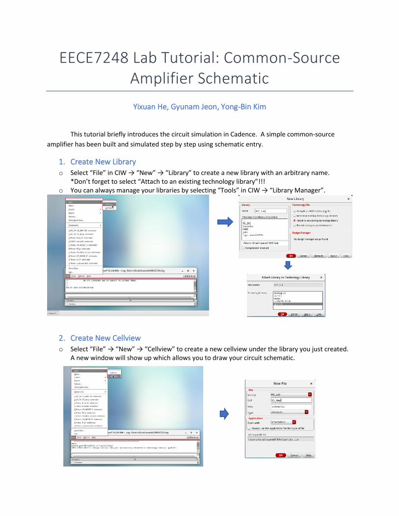
EECE7248 Lab Tutorial: Common-Source Amplifier Schematic
Yixuan He, Gyunam Jeon, Yong-Bin Kim
This tutorial briefly introduces the circuit simulation in Cadence. A simple common-source
amplifier has been built and simulated step by step using schematic entry.
1. Create New Library
o Select “File” in CIW → “New” → “Library” to create a new library with an arbitrary name. *Don’t forget to select “Attach to an existing technology library”!!!
o You can always manage your libraries by selecting “Tools” in CIW → “Library Manager”.
2. Create New Cellview
o Select “File” → “New” → “Cellview” to create a new cellview under the library you just created. A new window will show up which allows you to draw your circuit schematic.
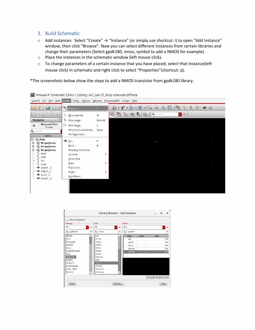
3. Build Schematic
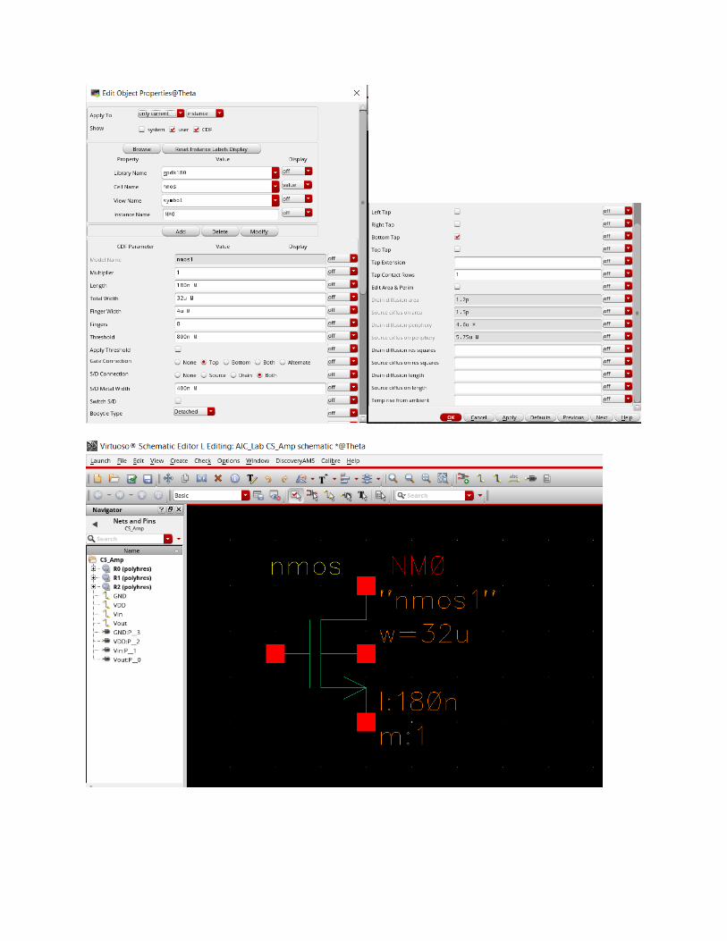
o Add instances: Select “Create” → “Instance” (or simply use shortcut: i) to open “Add Instance” window, then click “Browse”. Now you can select different instances from certain libraries and change their parameters (Select gpdk180, nmos, symbol to add a NMOS for example).
o Place the instances in the schematic window (left mouse click).
o To change parameters of a certain instance that you have placed, select that instance(left
mouse click) in schematic and right click to select “Proporties”(shortcut: q).
*The screenshots below show the steps to add a NMOS transistor from gpdk180 library.
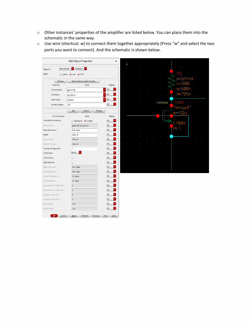
o Other instances’ properties of the amplifier are listed below. You can place them into the schematic in the same way.
o Use wire (shortcut: w) to connect them together appropriately (Press “w” and select the two
ports you want to connect). And the schematic is shown below.
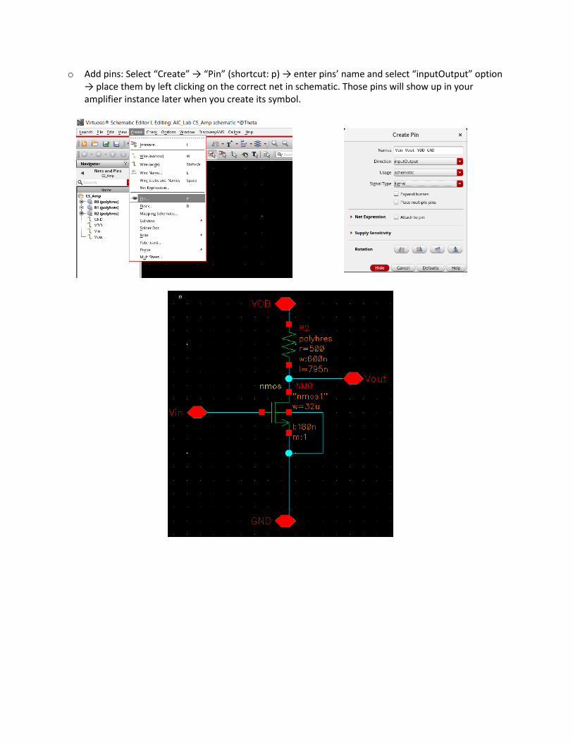
o Add pins: Select “Create” → “Pin” (shortcut: p) → enter pins’ name and select “inputOutput” option → place them by left clicking on the correct net in schematic. Those pins will show up in your amplifier instance later when you create its symbol.
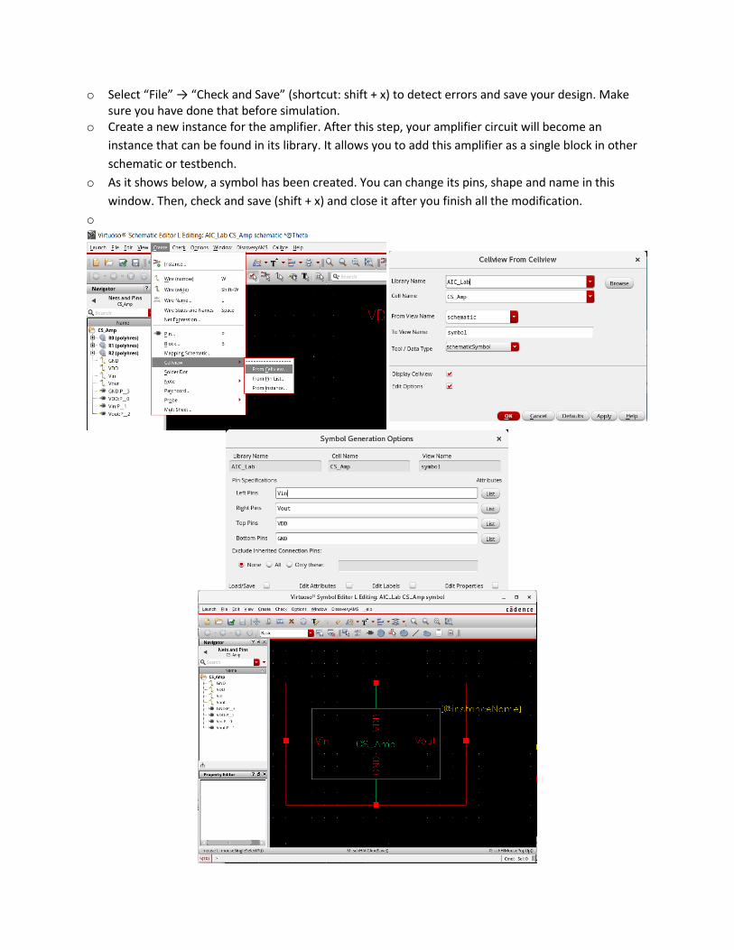
o Select “File” → “Check and Save” (shortcut: shift + x) to detect errors and save your design. Make sure you have done that before simulation.
o Create a new instance for the amplifier. After this step, your amplifier circuit will become an
instance that can be found in its library. It allows you to add this amplifier as a single block in other
schematic or testbench.
o As it shows below, a symbol has been created. You can change its pins, shape and name in this
window. Then, check and save (shift + x) and close it after you finish all the modification.
o
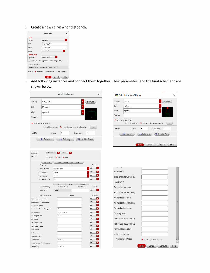
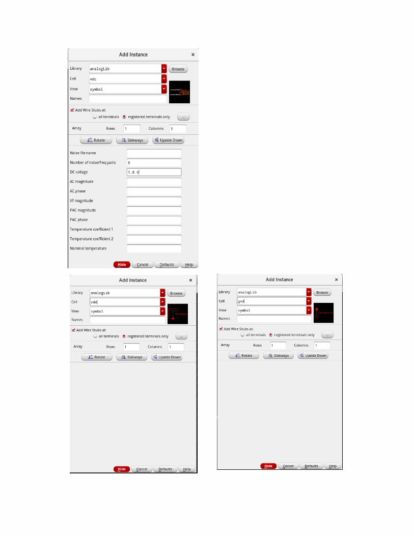
o Create a new cellview for testbench.
o Add following instances and connect them together. Their parameters and the final schematic are
shown below.
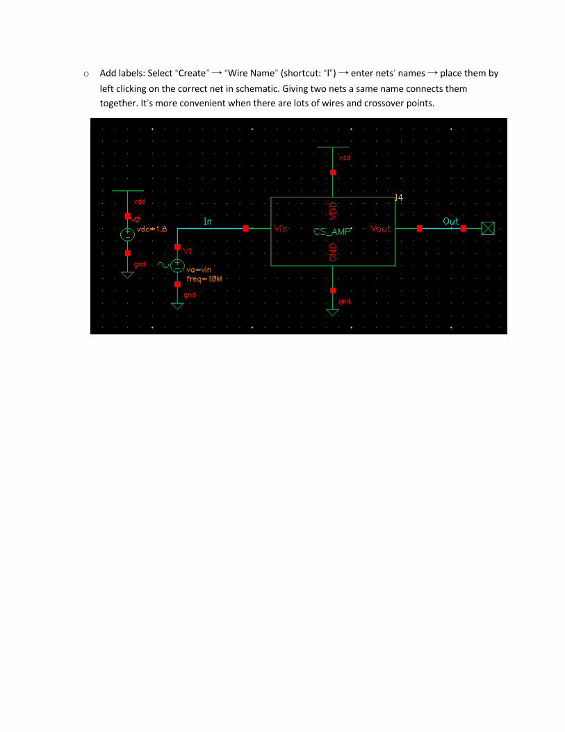
o Add labels: Select “Create” → “Wire Name” (shortcut: “l”) → enter nets’ names → place them by
left clicking on the correct net in schematic. Giving two nets a same name connects them
together. It’s more convenient when there are lots of wires and crossover points.
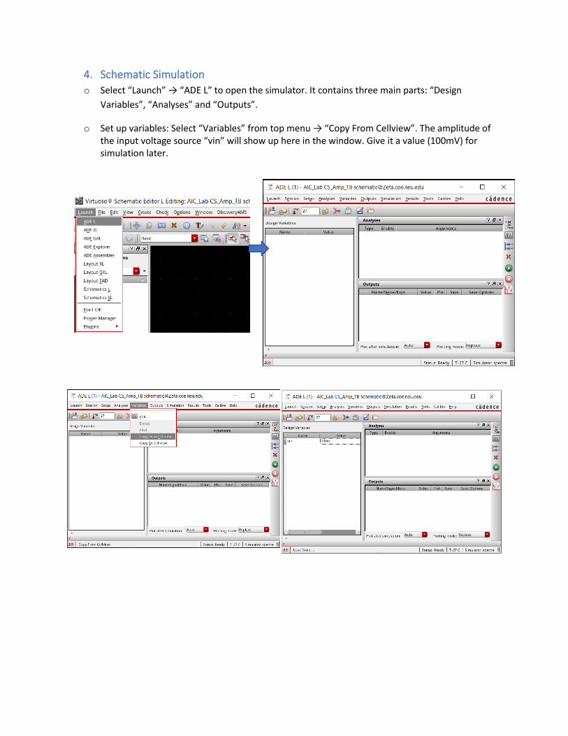
4. Schematic Simulation
o Select “Launch” → “ADE L” to open the simulator. It contains three main parts: “Design
Variables”, “Analyses” and “Outputs”.
o Set up variables: Select “Variables” from top menu → “Copy From Cellview”. The amplitude of the input voltage source “vin” will show up here in the window. Give it a value (100mV) for simulation later.
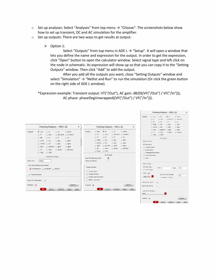
o Set up analyses: Select “Analyses” from top menu → “Choose”. The screenshots below show how to set up transient, DC and AC simulation for the amplifier.
o Set up outputs: There are two ways to get results at output.
➢ Option 1: Select “Outputs” from top menu in ADE L → “Setup”. It will open a window that
lets you define the name and expression for the output. In order to get the expression, click “Open” button to open the calculator window. Select signal type and left click on the node in schematic. Its expression will show up so that you can copy it to the “Setting Outputs” window. Then click “Add” to add the output.
After you add all the outputs you want, close “Setting Outputs” window and select “Simulation” → “Netlist and Run” to run the simulation (Or click the green button on the right side of ADE L window).
*Expression example: Transient output: VT("/Out"), AC gain: dB20((VF("/Out") / VF("/In"))),
AC phase: phaseDegUnwrapped((VF("/Out") / VF("/In"))).
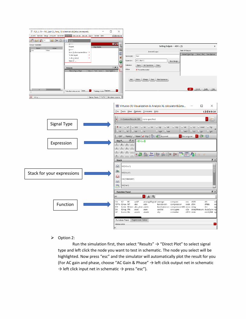
➢ Option 2:
Run the simulation first, then select “Results” → “Direct Plot” to select signal
type and left click the node you want to test in schematic. The node you select will be
highlighted. Now press “esc” and the simulator will automatically plot the result for you
(For AC gain and phase, choose “AC Gain & Phase” → left click output net in schematic
→ left click input net in schematic → press “esc”).
Signal Type
Expression
Stack for your expressions
Function
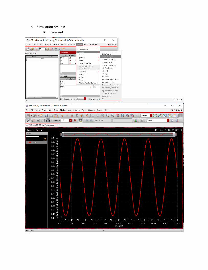
o Simulation results:
➢ Transient:
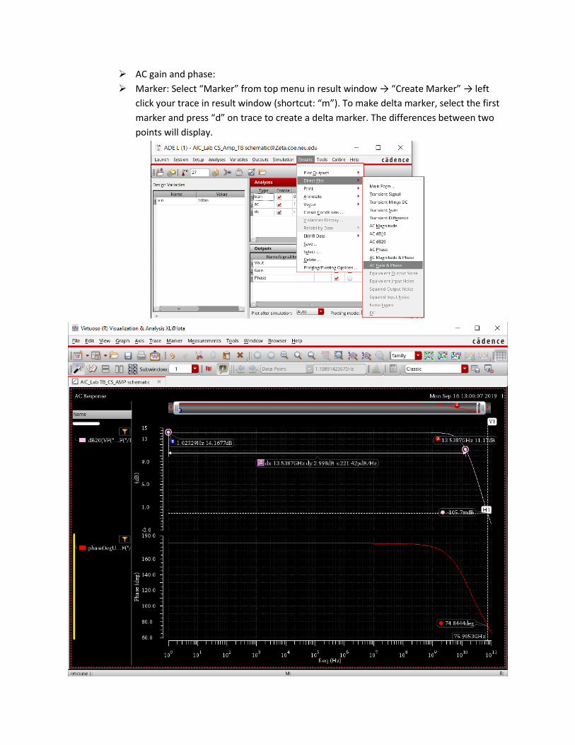
➢ AC gain and phase:
➢ Marker: Select “Marker” from top menu in result window → “Create Marker” → left
click your trace in result window (shortcut: “m”). To make delta marker, select the first
marker and press “d” on trace to create a delta marker. The differences between two
points will display.
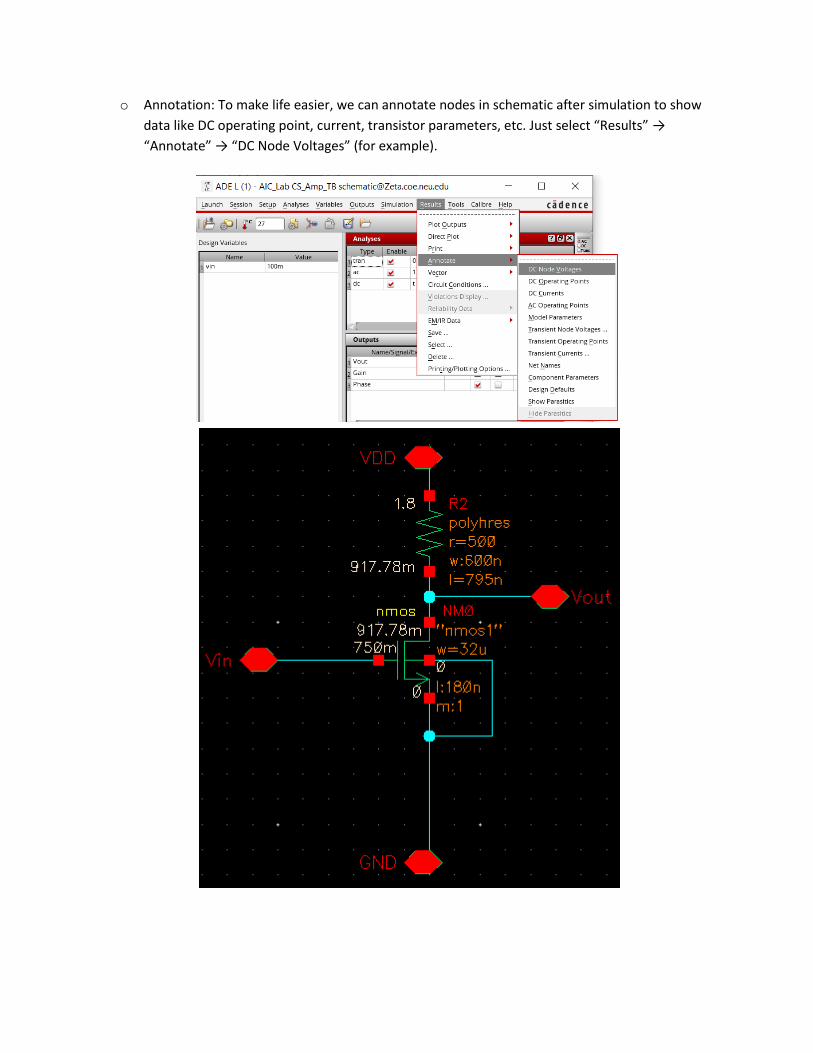
o Annotation: To make life easier, we can annotate nodes in schematic after simulation to show
data like DC operating point, current, transistor parameters, etc. Just select “Results” →
“Annotate” → “DC Node Voltages” (for example).
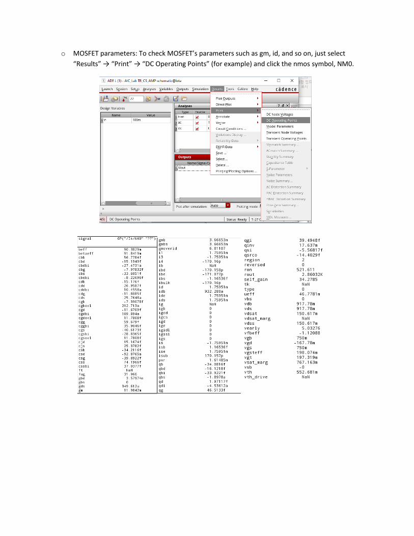
o MOSFET parameters: To check MOSFET’s parameters such as gm, id, and so on, just select
“Results” → “Print” → “DC Operating Points” (for example) and click the nmos symbol, NM0.
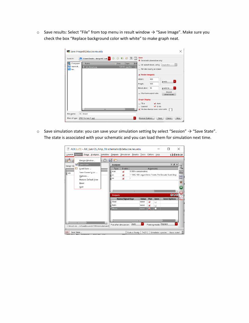
o Save results: Select “File” from top menu in result window → “Save Image”. Make sure you
check the box “Replace background color with white” to make graph neat.
o Save simulation state: you can save your simulation setting by select “Session” → “Save State”.
The state is associated with your schematic and you can load them for simulation next time.