Embed Size (px)
Citation preview

EE382V: System-on-Chip (SoC) Design Lecture 21
© 2014 A. Gerstlauer 1
EE382V:System-on-a-Chip (SoC) Design
Andreas GerstlauerElectrical and Computer Engineering
University of Texas at [email protected]
Lecture 21 – SoC Testing
Sources:Jacob A. Abraham
EE382V: SoC Design, Lecture 21 © 2014 A. Gerstlauer 2
Lecture 21: Outline
• SoC Manufacturing Test
• The testing problem
• SoC testing costs
• Design for Test (DFT)
• SoC Testability Features
• Boundary Scan
• P1500 standard
• Built-In Self Test
• Functional Test Access Mechanism (TAM)

EE382V: System-on-Chip (SoC) Design Lecture 21
© 2014 A. Gerstlauer 2
The Manufacturing Test Problem
EE382V: SoC Design, Lecture 21 © 2014 A. Gerstlauer 3
1982 1985 1988 1991 1994 1997 2000 2003 2006 2009
Co
st :
Cen
ts /
10,
000
Tran
sist
ors
1000.00
100.00
10.00
1.00
0.10
0.01
IC MfgCost
Cost ofTest
Mixed Signal
Digital
© J. A. Abraham
Partitioning for SoC Test
• Partition according to test methodology:• Logic blocks• Memory blocks• Analog blocks
• Provide test access:• Boundary scan• Analog test bus
• Provide test-wrappers for cores
Design for Test (DFT)
EE382V: SoC Design, Lecture 21 © 2014 A. Gerstlauer 4© J. A. Abraham
EE382V: System-on-Chip (SoC) Design Lecture 21
© 2014 A. Gerstlauer 3
DFT Architecture for SOC
EE382V: SoC Design, Lecture 21 © 2014 A. Gerstlauer 5
TR
ST
User defined test access mechanism (TAM)
Module
1Tes
t
wra
pper
Testsource
Testsink
Module
NTes
t
wra
pper
Test access port (TAP)
Functionalinputs
FunctionaloutputsFunc.
inputs
Func.outputs
SOC inputs SOC outputsTD
I
TC
K
TM
S
TD
O
Instruction register control
Serial instruction data
Source: Bushnell and Agrawal
© J. A. Abraham
Scan
• Convert each flip-flop to a scan register
• Only costs one extra multiplexer
• Normal mode: flip-flops behave as usual
• Scan mode: flip-flops behave as shift register
• Contents of flopscan be scannedout and new values scanned in
EE382V: SoC Design, Lecture 21 © 2014 A. Gerstlauer 6
Flo
p
QD
CLK
SI
SCAN
scan out
scan-in
inputs outputs
Flo
pF
lop
Flo
pF
lop
Flo
pF
lop
Flo
pF
lop
Flo
pF
lop
Flo
pF
lop
LogicCloud
LogicCloud
© J. A. Abraham

EE382V: System-on-Chip (SoC) Design Lecture 21
© 2014 A. Gerstlauer 4
Boundary Scan
• Testing boards is also difficult
• Need to verify solder joints are good– Drive a pin to 0, then to 1
– Check that all connected pins get the values
• Through-hold boards used “bed of nails”
• SMT and BGA boards cannot easily contact pins
Build capability of observing and controlling pins into each chip to make board test easier
EE382V: SoC Design, Lecture 21 © 2014 A. Gerstlauer 7© J. A. Abraham
Boundary Scan Example
EE382V: SoC Design, Lecture 21 © 2014 A. Gerstlauer 8
Serial Data In
Serial Data Out
Package Interconnect
IO pad and Boundary ScanCell
CHIP A
CHIP B CHIP C
CHIP D
© J. A. Abraham

EE382V: System-on-Chip (SoC) Design Lecture 21
© 2014 A. Gerstlauer 5
EE382V: SoC Design, Lecture 21 © 2014 A. Gerstlauer 9
Boundary Scan (IEEE 1149.1, JTAG)
© J. A. Abraham
Boundary Scan Interface
• Boundary scan is accessed through five pins
• TCK: test clock
• TMS: test mode select
• TDI: test data in
• TDO: test data out
• TRST*: test reset (optional)
• Chips with internal scan chains can access the chains through boundary scan for unified test strategy.
EE382V: SoC Design, Lecture 21 © 2014 A. Gerstlauer 10© J. A. Abraham

EE382V: System-on-Chip (SoC) Design Lecture 21
© 2014 A. Gerstlauer 6
Additional DFT Components
EE382V: SoC Design, Lecture 21 © 2014 A. Gerstlauer 11
Source: H. Kerkhoff
• Test source: Provides test vectors via on-chip LFSR, counter, ROM, or off-chip ATE.
• Test sink: Provides output verification using on-chip signature analyzer, or off-chip ATE.
• Test access mechanism (TAM): User-defined test data communication structure; carries test signals from source to module, and module to sink; tests module interconnects via test-wrappers; TAM may contain bus, boundary-scan and analog test bus components.
• Test controller: Boundary-scan test access port (TAP); receives control signals from outside; serially loads test instructions in test-wrappers.
© J. A. Abraham
Test Wrapper for a Core
EE382V: SoC Design, Lecture 21 © 2014 A. Gerstlauer 12
Source: H. Kerkhoff
© J. A. Abraham
• Logic added around a core to provide test access to the embedded core
• Test-wrapper provides for each core input terminal
• An external test mode – Wrapper element observes core input terminal for interconnect test
• An internal test mode – Wrapper element controls state of core input terminal for testing the logic inside core
• For each core output terminal
• A normal mode – Host chip driven by core terminal
• An external test mode – Host chip is driven by wrapper element for interconnect test
• An internal test mode – Wrapper element observes core outputs for core test

EE382V: System-on-Chip (SoC) Design Lecture 21
© 2014 A. Gerstlauer 7
A Test-Wrapper
EE382V: SoC Design, Lecture 21 © 2014 A. Gerstlauer 13
Wrappertest
controller
Scan chain
Sca
n ch
ain
Sca
n ch
ain
to/from TAP
from/toExternalTest pins
Wrapperelements
Core
Fun
ctio
nal
core
inpu
ts
Fun
ctio
nal
core
out
puts
Source: H. Kerkhoff
© J. A. Abraham
Goals of IEEE P1500
EE382V: SoC Design, Lecture 21 © 2014 A. Gerstlauer 14
Source: H. Kerkhoff
• Core test interface between embedded core and system chip
• Test reuse for embedded cores
• Testability guarantee for system interconnect and logic
• Improve efficiency of test between core users and core providers
© J. A. Abraham

EE382V: System-on-Chip (SoC) Design Lecture 21
© 2014 A. Gerstlauer 8
Set-up of P1500 Architecture
EE382V: SoC Design, Lecture 21 © 2014 A. Gerstlauer 15
Source: H. Kerkhoff
Core including Wrapper Cells
EE382V: SoC Design, Lecture 21 © 2014 A. Gerstlauer 16
Source: H. Kerkhoff
© J. A. Abraham

EE382V: System-on-Chip (SoC) Design Lecture 21
© 2014 A. Gerstlauer 9
Wrapper Registers for P1500
EE382V: SoC Design, Lecture 21 © 2014 A. Gerstlauer 17
Source: H. Kerkhoff
© J. A. Abraham
EE382V: SoC Design, Lecture 21 © 2014 A. Gerstlauer 18
Lecture 21: Outline
SoC Manufacturing Test
The testing problem
SoC testing costs
Design for test (DFT)
SoC Testability Features
Boundary Scan
P1500 standard
• Built-In Self Test
• Functional Test Access Mechanism (TAM)

EE382V: System-on-Chip (SoC) Design Lecture 21
© 2014 A. Gerstlauer 10
Built-In Self Test (BIST)
• Increasing circuit complexity, tester cost
• Interest in techniques which integrate some tester capabilities on the chip
• Reduce tester costs
• Test circuits at speed (more thoroughly)
• Approach:
• Compress test responses into “signature”
• Pseudo-random (or pseudo-exhaustive) pattern generator (PRG) on the chip
Integrating pattern generation and response evaluation on chip – BIST
EE382V: SoC Design, Lecture 21 © 2014 A. Gerstlauer 19© J. A. Abraham
EE382V: SoC Design, Lecture 21 © 2014 A. Gerstlauer 20
Pseudo-Random Sequences
• Linear Feedback Shift Register
• Shift register with input taken from XOR of state
• Pseudo-Random Sequence Generator
Flo
p
Flo
p
Flo
pQ[0] Q[1] Q[2]
CLK
D D D
111 (repeats)
70116001510040103101211011110QStep
Can also be used to
compress test responses
© J. A. Abraham

EE382V: System-on-Chip (SoC) Design Lecture 21
© 2014 A. Gerstlauer 11
EE382V: SoC Design, Lecture 21 © 2014 A. Gerstlauer 21
Example of BIST
Technique called
STUMPS
(from IBM)
© J. A. Abraham
Why is Conventional Test Successful?
• Two innovations have allowed test to keep up with complex designs
• The stuck-at fault model– The model allows structural test generation, with a number of faults which
is linear in the size of the circuit
• Partitioning the circuit– Partitioning the circuit (with scan latches for example), alleviates the test
problem so that test generation does not have to deal with the entire circuit
Do these two assumptions hold for Deep SubMicron(DSM) circuits?
EE382V: SoC Design, Lecture 21 © 2014 A. Gerstlauer 22© J. A. Abraham

EE382V: System-on-Chip (SoC) Design Lecture 21
© 2014 A. Gerstlauer 12
IC Technology
EE382V: SoC Design, Lecture 21 © 2014 A. Gerstlauer 23© J. A. Abraham
Features Smaller than Wavelengths
EE382V: SoC Design, Lecture 21 © 2014 A. Gerstlauer 24
Source: Raul Camposano, Synopsys
© J. A. Abraham
EE382V: System-on-Chip (SoC) Design Lecture 21
© 2014 A. Gerstlauer 13
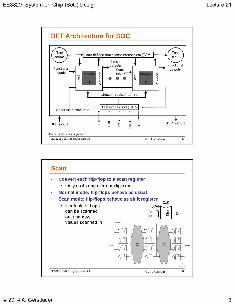
Increased Leakage
EE382V: SoC Design, Lecture 21 © 2014 A. Gerstlauer 25© J. A. Abraham
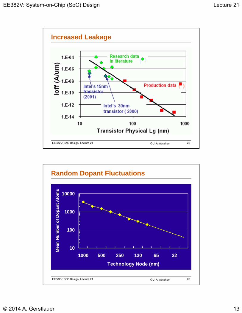
Random Dopant Fluctuations
EE382V: SoC Design, Lecture 21 © 2014 A. Gerstlauer 26
10
100
1000
10000
1000 500 250 130 65 32
Technology Node (nm)
Me
an
Nu
mb
er
of
Do
pa
nt
Ato
ms
© J. A. Abraham

EE382V: System-on-Chip (SoC) Design Lecture 21
© 2014 A. Gerstlauer 14
Defects in DSM Technologies
• Experiments on real chips (e.g., Stanford) • Stuck-at tests do not detect some defects unless they are
applied at speed
• Resistive opens comprise the bulk of test escapes in one production line• Likely in copper interconnect – cause delay faults
• Delay faults identified as the cause of most test escapes on another line• Speed differences of up to a factor of 1.5 can exist
between fast and slow devices - problems with “speed binning”
• Increasing possibility of shorts and crosstalk
EE382V: SoC Design, Lecture 21 © 2014 A. Gerstlauer 27© J. A. Abraham
Effects on Chip?
• Change in delays of paths
• Effects could be distributed across paths
EE382V: SoC Design, Lecture 21 © 2014 A. Gerstlauer 28
Solution:
• At-Speed tests
• Tester Cost?
• Apply “Native Mode”?
• Can use low-cost testersStuck-at Open Short Resistive
OpenLeakage Resistive
Short
At-Speed FunctionalStructural
Source: Gelsinger
At-speed functional tests better for delay defects
© J. A. Abraham

EE382V: System-on-Chip (SoC) Design Lecture 21
© 2014 A. Gerstlauer 15
Native-Mode Built-In Self Test
• Functional capabilities of processors can be used to replace BIST hardware – [UT Austin, ITC’1998]
• Application to self-test of processors at Intel – FRITS method applied to Pentium 4, Itanium [ITC’2002]
EE382V: SoC Design, Lecture 21 © 2014 A. Gerstlauer 29
for each data value Di {
Shift_Right_Through_Carry(S);
if (Carry) S = XOR(S, polynomial);
S = XOR(S, Di);
}
Hardware for MISR Software implementationof MISR
D D D D
Cn Cn-1 Cn-2 C1
D1 . . .
1 2 3 n
Q1 D2 DnQ2 Qn
© J. A. Abraham
Native-Mode Self Test for Processors
• Random instructions can be run from cache and results compressed into a signature
• Implementation in Intel FRITS system showed benefits for real chips (Pentium 4, Itanium)
• Technique can be used for self-test of an embedded processor in a System-on-Chip
Is it possible to now use this processing capability to test other modules (digital, analog/mixed-signal and RF) on the SoC?
• First, can the processor test be improved to detect realistic defects, e.g., small delays?
EE382V: SoC Design, Lecture 21 © 2014 A. Gerstlauer 30© J. A. Abraham

EE382V: System-on-Chip (SoC) Design Lecture 21
© 2014 A. Gerstlauer 16
Are Random Tests Sufficient?
• Intel implementation involved code in the cache which generated random instruction sequences
• Interest in generating instructions targeting faults
• Possible to generate instruction sequences which will test for an internal stuck-at fault in a module [Gurumurthy, Vasudevan and Abraham, ITC 2006]
• In order to deal with defects in DSM technologies, need to target small delay defects
• Recent work: automatically generate instruction sequences which will target small delay defects in an internal module [Gurumurthy, Vemu, Abraham and Saab, European Test Symposium (ETS) 2007]
EE382V: SoC Design, Lecture 21 © 2014 A. Gerstlauer 31© J. A. Abraham
Test Access Mechanisms (TAMs)
• Non-functional access
• Uses a kind of access to core not allowed during the normal functional operation
• Generally based on scan chains or other design for test (DFT) structures
• Can also use the embedded processor as the test source/sink → Needs wrappers around the core under test
• Functional access
• Embedded processor is the test source/sink → No DFT structures or wrappers around the cores
EE382V: SoC Design, Lecture 21 © 2014 A. Gerstlauer 32© J. A. Abraham
EE382V: System-on-Chip (SoC) Design Lecture 21
© 2014 A. Gerstlauer 17
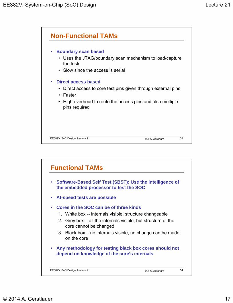
Non-Functional TAMs
• Boundary scan based
• Uses the JTAG/boundary scan mechanism to load/capture the tests
• Slow since the access is serial
• Direct access based
• Direct access to core test pins given through external pins
• Faster
• High overhead to route the access pins and also multiple pins required
EE382V: SoC Design, Lecture 21 © 2014 A. Gerstlauer 33© J. A. Abraham
Functional TAMs
• Software-Based Self Test (SBST): Use the intelligence of the embedded processor to test the SOC
• At-speed tests are possible
• Cores in the SOC can be of three kinds
1. White box -- internals visible, structure changeable
2. Grey box – all the internals visible, but structure of the core cannot be changed
3. Black box – no internals visible, no change can be made on the core
• Any methodology for testing black box cores should not depend on knowledge of the core’s internals
EE382V: SoC Design, Lecture 21 © 2014 A. Gerstlauer 34© J. A. Abraham

EE382V: System-on-Chip (SoC) Design Lecture 21
© 2014 A. Gerstlauer 18
Generatesoftware
Test stimuli
Reverse driver
code
loaded intoSoftware to be
the processor
Data values
[Gurumurthy, Sambamurthy and Abraham, Int'l Test Synthesis Workshop (ITSW) 2008]
Approach to Testing Cores
• Uses functional TAM
• Uses pre-existing vectors
• Generates software to be loaded on to the embedded processor
• Reverse driver that producesgiven test vectors for core
EE382V: SoC Design, Lecture 21 © 2014 A. Gerstlauer 35© J. A. Abraham
Pre-Existing Vectors
• If using a core bought from vendor
• Vectors might also be provided by the vendor
• Reusing a core
• Vectors from the previous use
• Newly designed core
• Validation vectors
• Only constraint: these vectors must be functional test patterns for the core
EE382V: SoC Design, Lecture 21 © 2014 A. Gerstlauer 36© J. A. Abraham

EE382V: System-on-Chip (SoC) Design Lecture 21
© 2014 A. Gerstlauer 19
Reverse Driver
• Parses the vector sequence to generate the data set to be sent to the core being tested
• Is specific to each core – as many as the number of driver programs
• Only overhead involved
• Generates the output in a format readable by the driver program
EE382V: SoC Design, Lecture 21 © 2014 A. Gerstlauer 37© J. A. Abraham
Address Data
0x00 0x07
0x01 0x54
0x02 0xDF
0x03 0x71
0x04 0x78
Reverse
Driver
Send at speed rate 1Data 0x0754DF7178
Reverse Driver Illustration
• Peripheral core communicating with external environment (send/receive 32-bit data)
• Five 8-bit registers addresses 0 – 4
• Register 0 – Control
• Registers 1 to 4 – Data
EE382V: SoC Design, Lecture 21 © 2014 A. Gerstlauer 38© J. A. Abraham

EE382V: System-on-Chip (SoC) Design Lecture 21
© 2014 A. Gerstlauer 20
Software Generation
• Use the driver program associated with each core being tested
• Driver programs
• Software code that actually talks with the non-processor cores
• Know about the bus protocol
• Generally able to take in the data to be sent to the core or read back data from the core
• Developed as part of designing the SOC
EE382V: SoC Design, Lecture 21 © 2014 A. Gerstlauer 39© J. A. Abraham
Coverage Measurement
• Simulate the SOC using the software generated
• Platform used SOC validation can be used
• Monitor the core boundaries to capture the pin data
• Fault simulate the core with the captured data
EE382V: SoC Design, Lecture 21 © 2014 A. Gerstlauer 40© J. A. Abraham
EE382V: System-on-Chip (SoC) Design Lecture 21
© 2014 A. Gerstlauer 21
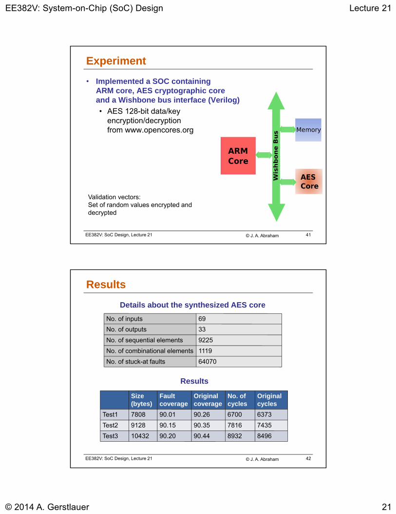
Validation vectors:Set of random values encrypted and decrypted
Experiment
• Implemented a SOC containing ARM core, AES cryptographic core and a Wishbone bus interface (Verilog)
• AES 128-bit data/key encryption/decryption from www.opencores.org
EE382V: SoC Design, Lecture 21 © 2014 A. Gerstlauer 41© J. A. Abraham
No. of inputs 69
No. of outputs 33
No. of sequential elements 9225
No. of combinational elements 1119
No. of stuck-at faults 64070
Details about the synthesized AES core
Size (bytes)
Fault coverage
Original coverage
No. of cycles
Original cycles
Test1 7808 90.01 90.26 6700 6373
Test2 9128 90.15 90.35 7816 7435
Test3 10432 90.20 90.44 8932 8496
Results
Results
EE382V: SoC Design, Lecture 21 © 2014 A. Gerstlauer 42© J. A. Abraham

EE382V: System-on-Chip (SoC) Design Lecture 21
© 2014 A. Gerstlauer 22
Lecture 21: Summary
• SoC Manufacturing Test
• Scan chains
• JTAG Boundary Scan
• Test wrappers for cores
• Built-in self test (BIST)
• Advanced SoC test topics
• Analog/Mixed-Signal (AMS) test
• RF test
• Micro-Electro-Mechanical Systems (MEMS) test
EE382V: SoC Design, Lecture 18 © 2014 A. Gerstlauer 43