Embed Size (px)
Citation preview
Innovation with Integrity
Max Patzschke, Andi Kaeppel
Bruker Nano GmbH
EDS Analysis Using Ultra–Low Beam Currents
• Multiple element SDDs
• XFlash® 5060FQ
• Examples of fast/large area SEM/T-SEM-EDS using the FQ
Presenters
Max Patzschke
Application Scientist,Bruker Nano Analytics, Berlin, Germany
Andi Kaeppel
Product Manager EDS/SEM, Bruker Nano Analytics, Berlin, Germany
2

• Introducing the X-Flash FlatQuad• Chip area vs. take of angle• Examples:• -high speed mapping• -large area maps• - samples without sample preparation• -samples with high topography • -Low kV analysis on sensitive samples and nano particles
Overview
3

• Detector combines high count rate capabilities with high collection efficiency (solid angle)
• Application fields are:
• Particles or structures in nanometer range (low kV, smaller excitation volume)
• Beam sensitive samples (low probe current)
• Samples with high topography (avoids shadowing effects)
• Light element samples (low kV for ideal ionization cross-section)
• Thin (electron transparent) samplee.g. TEM/STEM samples (low x-ray yield)
• Ultra fast spectral mapping
• Large area mapping: mapping of neighboring areas and stitch maps together
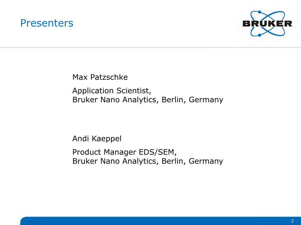
XFlash® 5060FQ
4

Four channel SDD: XFlash® 5060FQ
5
Flat QUAD detector in combination with a conventional XFlashdetector at the Hitachi SU8000 series (Cold-Emission FE-SEM)
XFlash® 5060FQ
• 4x15mm²=60mm²
• capable of output count rates up to 4 x 400,000 cps= 1,600,000 cps
• annular design
• Central aperture for the primary beam
6

Advantage of four elements Count rate capability
Output vs Input count rate, four channel SDD, 400kcps processors
7
1800
1500
1200
900
600
300
0
OC
R /
kcps
0 750 1500 2250 3000 3750 4500ICR / kcps
OCR of up to 4 x 400,000 cps= 1,600,000 cps
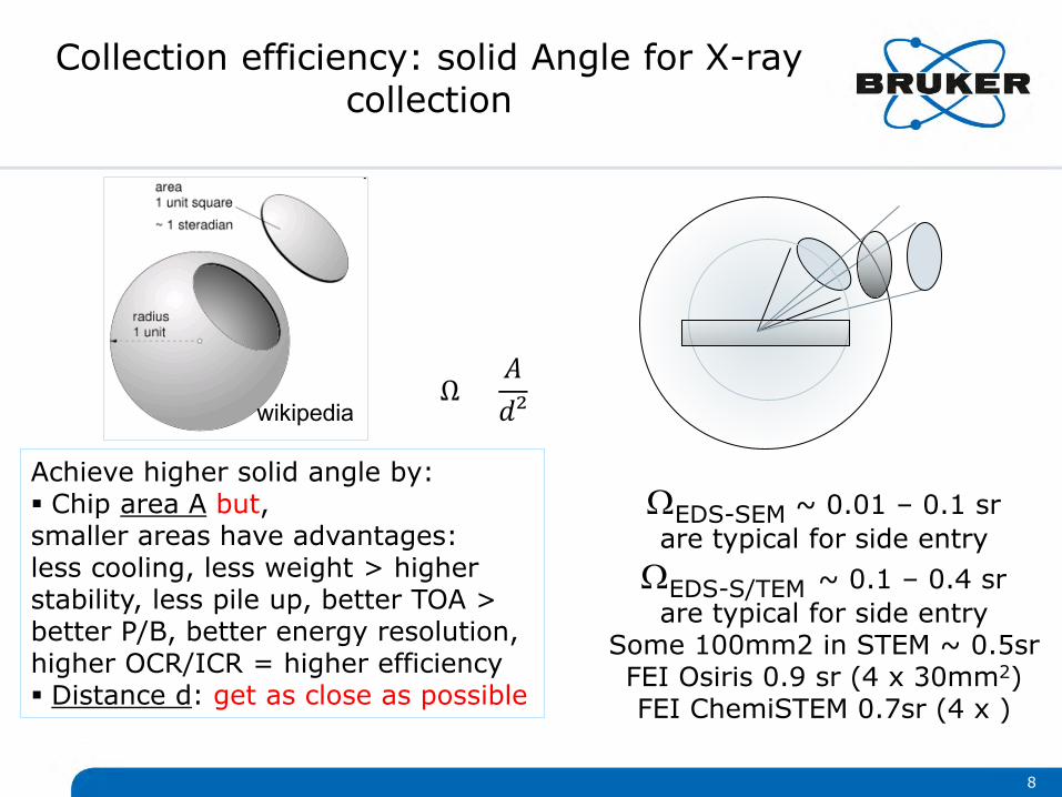
Collection efficiency: solid Angle for X-ray collection
wikipedia
Ω = Asurf / r2 [sr]ΩEDS-SEM ~ 0.01 – 0.1 srare typical for side entry
ΩEDS-S/TEM ~ 0.1 – 0.4 srare typical for side entry
Some 100mm2 in STEM ~ 0.5srFEI Osiris 0.9 sr (4 x 30mm2)FEI ChemiSTEM 0.7sr (4 x )
Achieve higher solid angle by: Chip area A but, smaller areas have advantages:less cooling, less weight > higher stability, less pile up, better TOA >better P/B, better energy resolution, higher OCR/ICR = higher efficiency Distance d: get as close as possible
Ω =𝐴𝐴𝑑𝑑𝑑
8
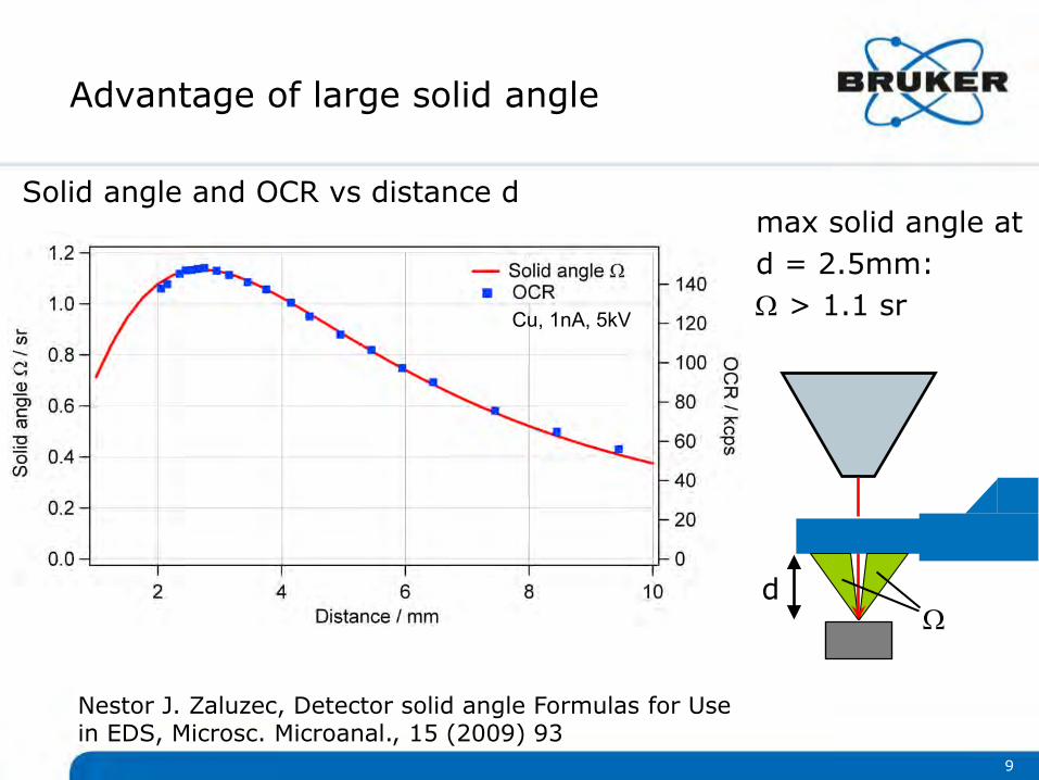
Advantage of large solid angle
max solid angle atd = 2.5mm:Ω > 1.1 sr
dΩ
Solid angle and OCR vs distance d
Nestor J. Zaluzec, Detector solid angle Formulas for Usein EDS, Microsc. Microanal., 15 (2009) 93
Cu, 1nA, 5kV
9
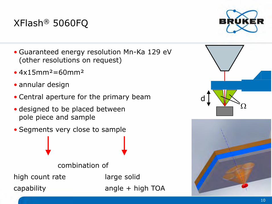
XFlash® 5060FQ
dΩ
• Guaranteed energy resolution Mn-Ka 129 eV (other resolutions on request)
• 4x15mm²=60mm²
• annular design
• Central aperture for the primary beam
• designed to be placed between pole piece and sample
• Segments very close to sample
combination ofhigh count rate large solidcapability angle + high TOA
10
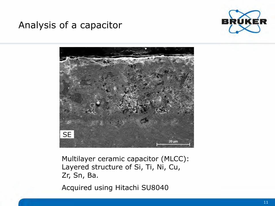
Analysis of a capacitor
11
Multilayer ceramic capacitor (MLCC): Layered structure of Si, Ti, Ni, Cu, Zr, Sn, Ba.
Acquired using Hitachi SU8040
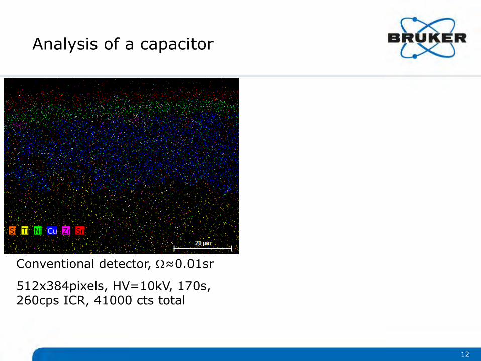
Analysis of a capacitor
12
Conventional detector, Ω≈0.01sr
512x384pixels, HV=10kV, 170s, 260cps ICR, 41000 cts total

Analysis of a capacitor
13
Conventional detector, Ω≈0.01sr
512x384pixels, HV=10kV, 170s, 260cps ICR, 41000 cts total
XFlash® 5060FQ
512x384pixels, HV=10kV, 170s, 28kcps ICR, 4800000 cts total (same beam current)
Ω≈1sr> 100x
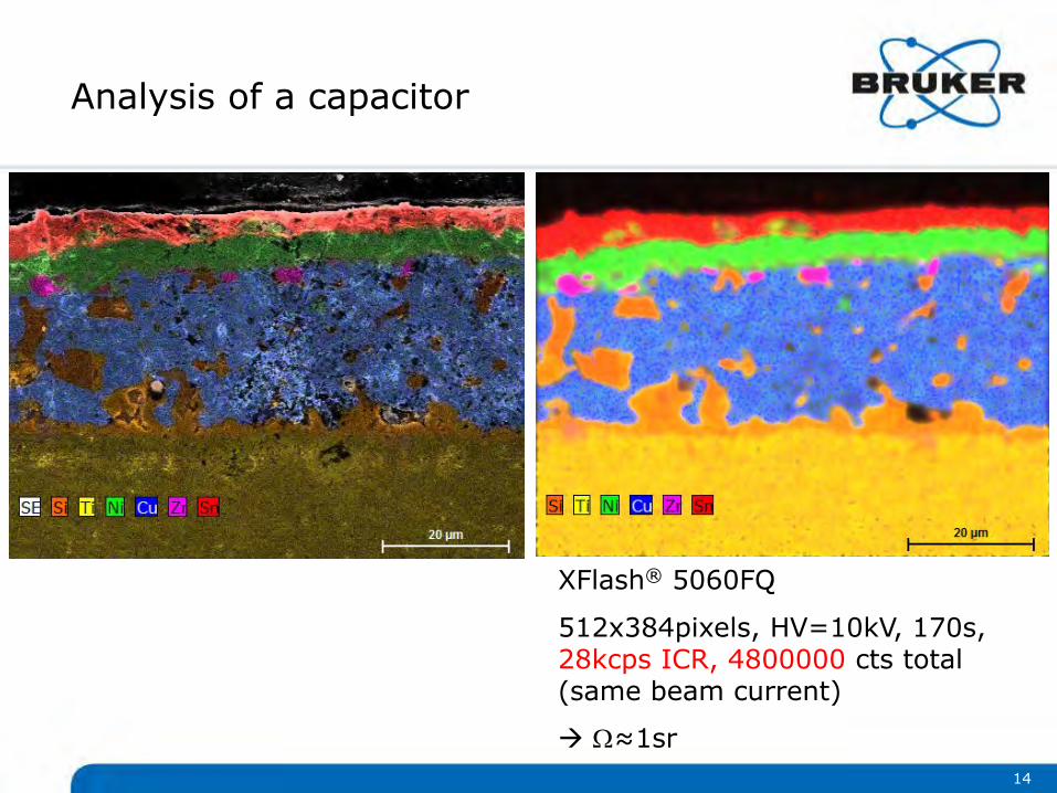
Analysis of a capacitor
14
XFlash® 5060FQ
512x384pixels, HV=10kV, 170s, 28kcps ICR, 4800000 cts total (same beam current)
Ω≈1sr
Analysis of a capacitor
15
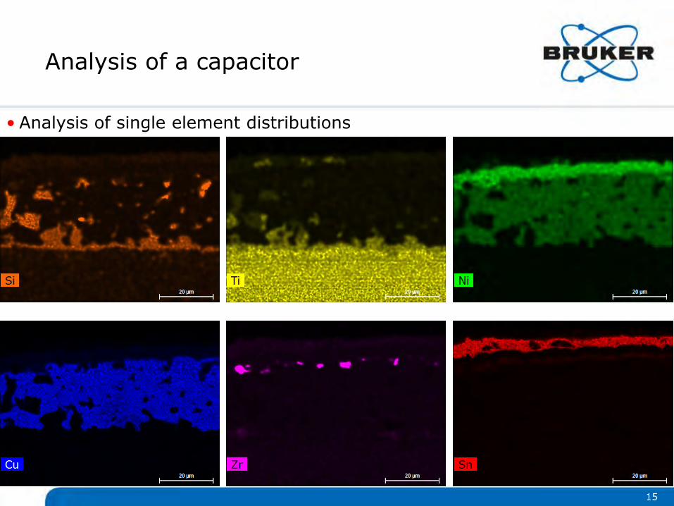
• Analysis of single element distributions
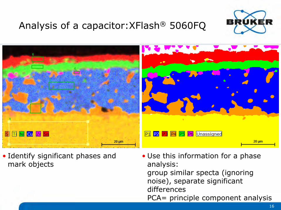
Analysis of a capacitor:XFlash® 5060FQ
16
• Identify significant phases andmark objects
• Use this information for a phaseanalysis: group similar specta (ignoringnoise), separate significantdifferencesPCA= principle component analysis

Analysis of a capacitor
17
• Investigate the sum spectra of the phases

Analysis of a capacitor
18
SnPlating
NiBarrier
CuTermination
BaTiO3dielectric
layer
• A lot of analysis methods can be applied to dataacquired in only 3 minutes!

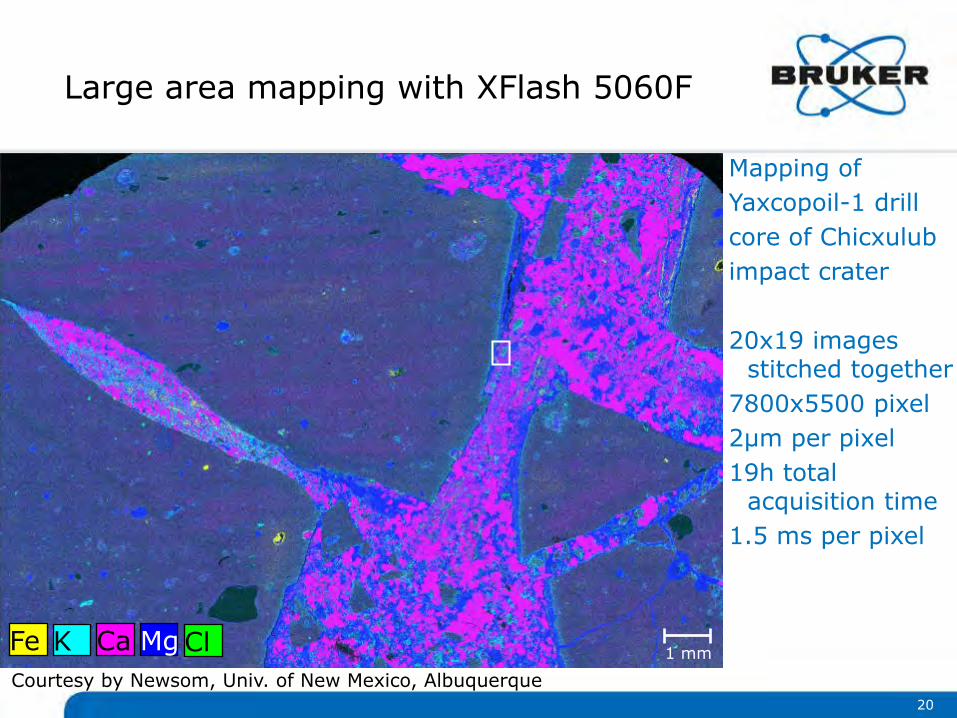
Large area mapping with XFlash 5060F
Courtesy by Newsom, Univ. of New Mexico, Albuquerque
Mapping ofYaxcopoil-1 drillcore of Chicxulubimpact crater
20x19 imagesstitched together
7800x5500 pixel2µm per pixel19h total
acquisition time1.5 ms per pixel
19
Large area mapping with XFlash 5060F
Courtesy by Newsom, Univ. of New Mexico, Albuquerque1 mmFe K Ca Mg Cl
Mapping ofYaxcopoil-1 drillcore of Chicxulubimpact crater
20x19 imagesstitched together
7800x5500 pixel2µm per pixel19h total
acquisition time1.5 ms per pixel
20
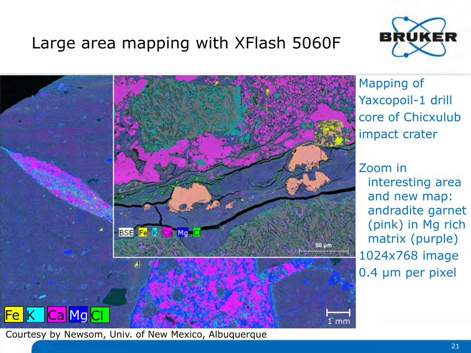
Large area mapping with XFlash 5060F
21Courtesy by Newsom, Univ. of New Mexico, Albuquerque
Mapping ofYaxcopoil-1 drillcore of Chicxulubimpact crater
Zoom in interesting area and new map: andradite garnet (pink) in Mg rich matrix (purple)
1024x768 image0.4 µm per pixel
Fe K Ca Mg Cl 1 mm

φ=30..35°
Take-off angle comparison: XFlash® 5060FQ vs. conventional SDDs:
Advantage of high take-off angle andannular design
22
φ=60..70°
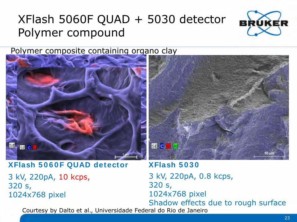
Polymer composite containing organo clay
2 µm
XFlash 5060F QUAD + 5030 detectorPolymer compound
XFlash 5060F QUAD detector XFlash 5030
Courtesy by Dalto et al., Universidade Federal do Rio de Janeiro
3 kV, 220pA, 10 kcps, 320 s,1024x768 pixel
3 kV, 220pA, 0.8 kcps, 320 s,1024x768 pixelShadow effects due to rough surface
23

Analysis of samples with high topography
24
Sample containing C, Si, SiC
• Rough, broken-off surface, showing cracks and recess structures
• Difficult to analyze because of inclined surfaces
• Large absorption effects possible, especially for carbon
• Analyzed with Hitachi SU8040 cold cathode FE-SEM at HV=3kV

Analysis of samples with high topography
25
Mapping of C, Si
512x384pixels, HV=3kV, 170s, 7.5kcps ICR, 1,200,000 cts total
Sample containing Si, SiC, C
• Mapping of carbon and silicon shows C rich (red), Si rich (blue, upper left) and Si-C containing phases

Analysis of samples with high topography
26
Mapping of C, Si
512x384pixels, HV=3kV, 170s, 7.5kcps ICR, 1,200,000 cts total
Sample containing Si, SiC, C
• Application of an automatic phase analysis (combination of similar spectra) reveals more clearly the three different phases
• Almost independent of the topography
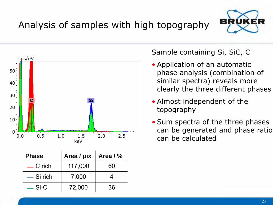
Analysis of samples with high topography
27
Sample containing Si, SiC, C
• Application of an automatic phase analysis (combination of similar spectra) reveals more clearly the three different phases
• Almost independent of the topography
• Sum spectra of the three phases can be generated and phase ratio can be calculated
Phase Area / pix Area / %C rich 117,000 60
Si rich 7,000 4
Si-C 72,000 36

Analysis of samples with high topography
28
Sample containing Si, SiC, C
• Application of an automatic phase analysis (combination of similar spectra) reveals more clearly the three different phases
• Almost independent of the topography
• Sum spectra of the three phases can be generated and phase ratio can be calculated
• Sum spectra can be quantitatively analyzed and indicate a C, Si and SiC phase
• Restrictions: C absorption effects due to inclined facets
Phase C / at.% Si / at.%C rich 98 2
Si rich 15 85
Si-C 45 55

Sample courtesy: L. Ferrière, Naturhistorisches Museum Wien
High vacuum analysis at low beam currentHistoric stony meteorite (“Mocs”)
XFlash® 5060F, Hitachi SU6600, 6 kV, <10 pA, 2 kcps, 47 min
• Fell 3rd February 1882 • Sample preparation
(coating) exluded• Lead contamination
(old polishing)• Pb-M and S-K can be
deconvolved using an online routine
1.80 2.00 2.20 2.40 2.60 2.80keV
0
1
2
3
4
5
6
7 cps/eV
S Pb
Lead deposition in cracks
Iron nickel sulfides
29
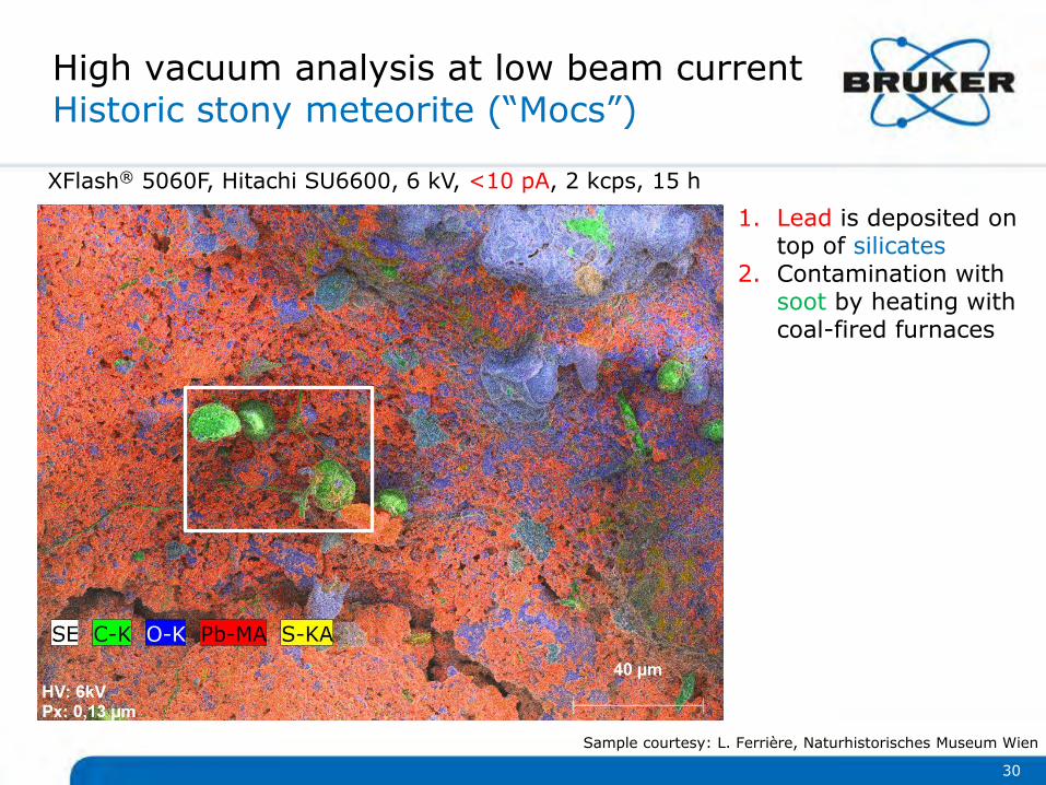
Sample courtesy: L. Ferrière, Naturhistorisches Museum Wien
XFlash® 5060F, Hitachi SU6600, 6 kV, <10 pA, 2 kcps, 15 h
1. Lead is deposited on top of silicates
2. Contamination withsoot by heating withcoal-fired furnaces
High vacuum analysis at low beam currentHistoric stony meteorite (“Mocs”)
30

Sample courtesy: L. Ferrière, Naturhistorisches Museum Wien
High vacuum analysis at low beam currentHistoric stony meteorite (“Mocs”)
<300 nm!
• Cultural heritage samples can be analyzed at the sub-µm scale without any sample preparation
• EDS at high vacuum offers better spatial resolution compared to low vacuum
XFlash® 5060F, Hitachi SU6600, 6 kV, <10 pA, 2 kcps, 15 h
31
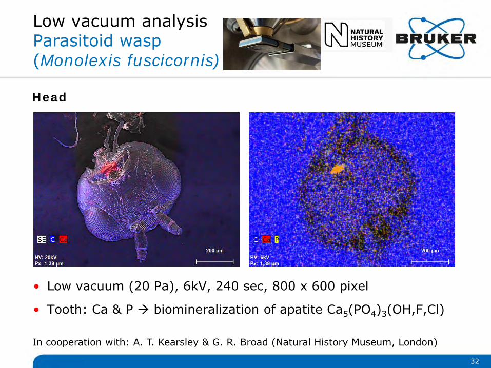
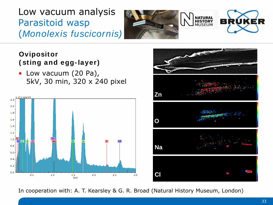
Low vacuum analysisParasitoid wasp (Monolexis fuscicornis)
32
Head
In cooperation with: A. T. Kearsley & G. R. Broad (Natural History Museum, London)
• Low vacuum (20 Pa), 6kV, 240 sec, 800 x 600 pixel
• Tooth: Ca & P biomineralization of apatite Ca5(PO4)3(OH,F,Cl)
Low vacuum analysisParasitoid wasp (Monolexis fuscicornis)
33
In cooperation with: A. T. Kearsley & G. R. Broad (Natural History Museum, London)
• Low vacuum (20 Pa), 5kV, 30 min, 320 x 240 pixel
Ovipositor (sting and egg-layer)
Zn
O
Na
Cl
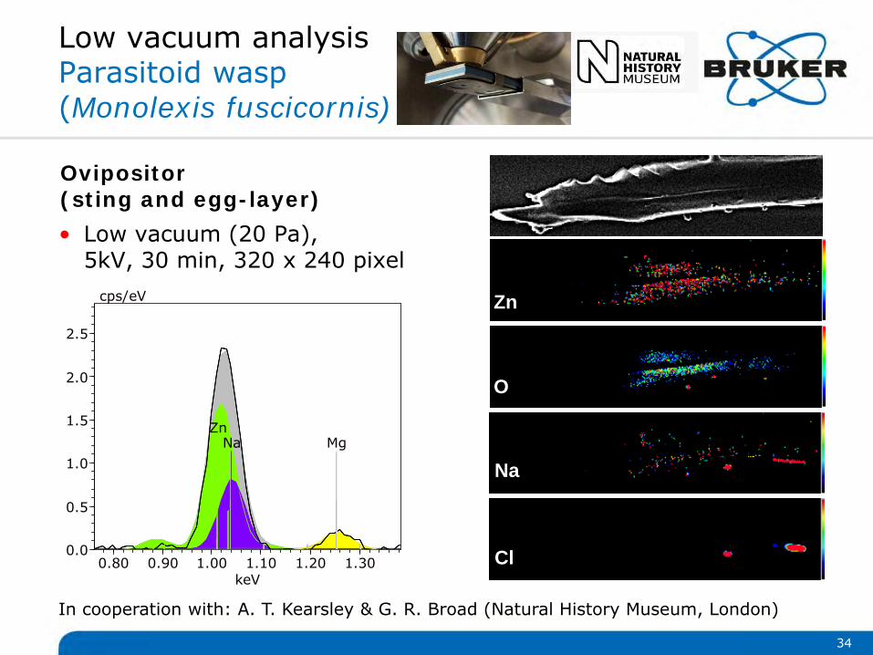
Low vacuum analysisParasitoid wasp (Monolexis fuscicornis)
34
In cooperation with: A. T. Kearsley & G. R. Broad (Natural History Museum, London)
• Low vacuum (20 Pa), 5kV, 30 min, 320 x 240 pixel
Ovipositor (sting and egg-layer)
0.80 0.90 1.00 1.10 1.20 1.30keV
0.0
0.5
1.0
1.5
2.0
2.5
cps/eV
Mg Na
Zn
Zn
O
Na
Cl

NASA Stardust mission: spacecraft collected samples of a comet and returned them to Earth
35
• Test experiments necessary
• Micro crater generated by meteor like projectiles in Al foil
stardust.jpl.nasa.gov

25.07.2016 36
HyperMap: 3600x2700 pixel, 10keV, 1.0 Mcps ICR, 620 s,41 counts/pixel, reduced shadow effects
HyperMap / Spectral image / proof of principle exp.Micro crater generated by meteor like projectiles inAl foil, Hitachi SU6600 Schottky FE-SEM
Kearsley et al. 2011, Salge et al. 2011
25.07.2016 37
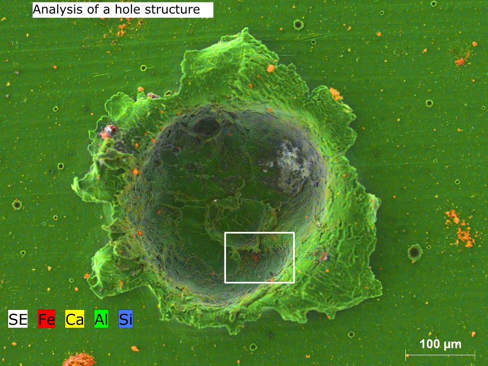
Analysis of a hole structure

25.07.2016 38
Magnified area: 480x360 pixel

TSEM-EDX of NPTypical Overview
39

40
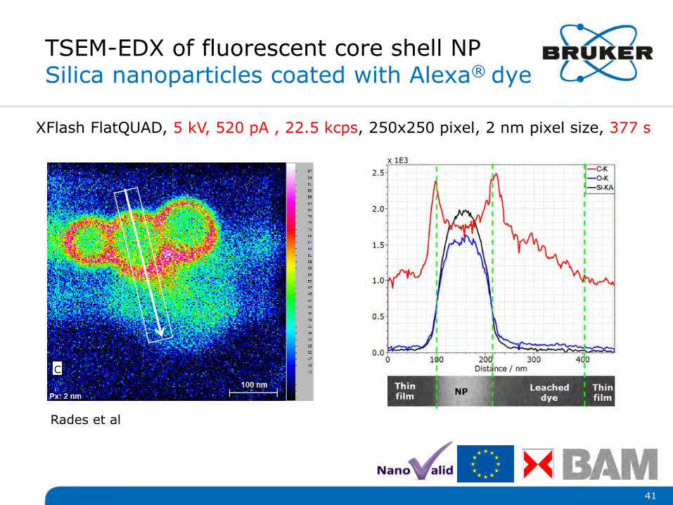
TSEM-EDX of fluorescent core shell NPSilica nanoparticles coated with Alexa® dye
XFlash FlatQUAD, 5 kV, 520 pA , 22.5 kcps, 250x250 pixel, 2 nm pixel size, 377 s
K. Natte, T. Behnke, G. Orts-Gil, C. Würth, J. F. Friedrich, W. Österle and U. Resch-Genger, J Nanopart Res, 2012, 14, 680
41
TSEM-EDX of fluorescent core shell NPSilica nanoparticles coated with Alexa® dye
XFlash FlatQUAD, 5 kV, 520 pA , 22.5 kcps, 250x250 pixel, 2 nm pixel size, 377 s
Rades et al

42
TSEM-EDX of NPClassification
„bulk“ NP „hollow“ NP
Hodoroaba et al
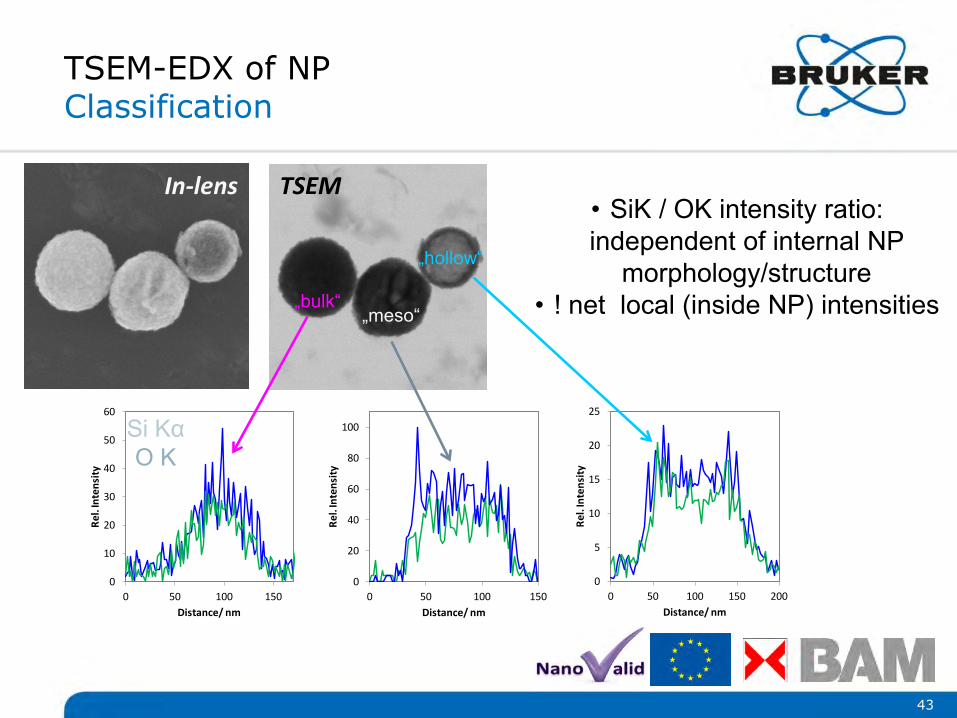
43
TSEM-EDX of NPClassification
0
10
20
30
40
50
60
0 50 100 150
Rel.
Inte
nsity
Distance/ nm
0
20
40
60
80
100
0 50 100 150
Rel.
Inte
nsity
Distance/ nm
0
5
10
15
20
25
0 50 100 150 200Re
l. In
tens
ity
Distance/ nm
„hollow“
„meso“„bulk“
In-lens TSEM
Si KαO K
• SiK / OK intensity ratio: independent of internal NP
morphology/structure• ! net local (inside NP) intensities

44
TSEM-EDX of NPClassification
„bulk“ NP
„hollow“ NP
unclassified NPSDD10 mm2
Flat QUAD
Acq time (s per NP) 120 2
ICR (kcps) 0.3 ≥20
Sol angle (sr) 0.01 1
NP identified 25 127
45
Summary
• The XFlash® 5060FQ offers highest solid angle (1.1sr) + 4 x single throughput (1.600.000 cts) and collection angle of 60°– 70°
• allowing for
- Ultra fast mapping
- Nano particles
- large area mapping
- high topography no shadow effects
- Beam sensitive samples,
- SEM/T-SEM-EDS of
- bulk and
- electron transparent samples,

46
GeozentrumNordbayernP. Schulte
Natural HistoryMuseum London
A. KearsleyG. Broad
Ocean Drilling Program
Federal Institute for Materials Research
and TestingD. Hodoroaba,
European Union
grant agreement n 263147… Risk assessmenst …
Institute of Meteoritics, University ofNew MexicoH. Newsom
Q&A
47
Are There Any Questions?
Please type in the questions you have
in the Q&A box, select Ask: “All panelists” and press Send.

Innovation with Integrity
Copyright © 2016 Bruker Corporation. All rights reserved. www.bruker.com