Embed Size (px)
Citation preview
AXI Interfacing
IP Creation
ECE 699: Lecture 5

Required Reading
• Tutorial 4: IP Creation • Exercise 4A: Creating IP in HDL
The ZYNQ Book Tutorials
• Chapter 19: AXI Interfacing The ZYNQ Book
ARM AMBA AXI Protocol v1.0: Specification • Chapter 1: Introduction • Chapter 2: Signal Descriptions • Chapter 3: Channel Handshake • Chapter 4: Addressing Options • Chapter 9: Data Buses
Recommended Reading
• Chapter 10: On-Chip Buses
P. Schaumont, A Practical Introduction to Hardware/Software Codesign, 2nd Ed.
M.S. Sadri, ZYNQ Training (presentations and videos)
• Lesson 1 : What is AXI? • Lesson 2 : What is an AXI Interconnect? • Lesson 3 : AXI Stream Interface
Source: M.S. Sadri, Zynq Training
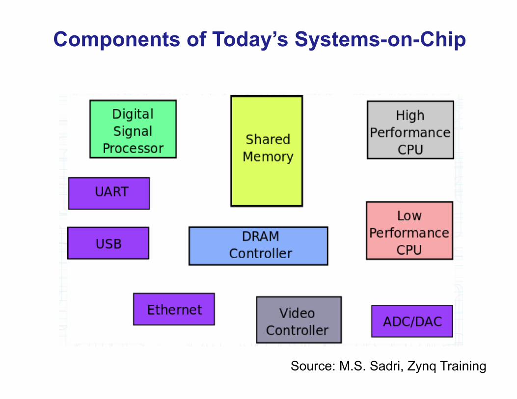
Components of Today’s Systems-on-Chip
Source: M.S. Sadri, Zynq Training
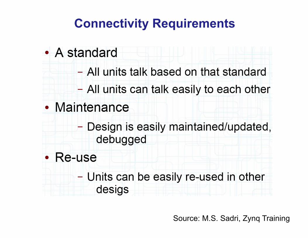
Connectivity Requirements
Source: M.S. Sadri, Zynq Training
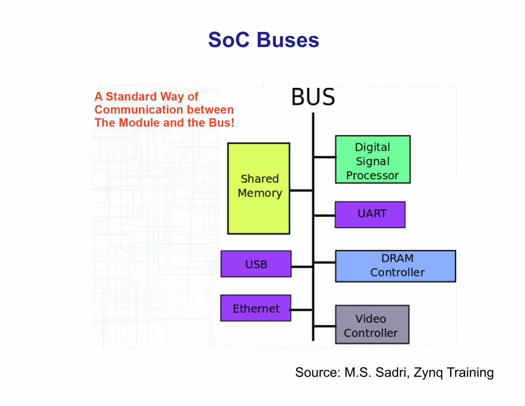
SoC Buses
Source: M.S. Sadri, Zynq Training
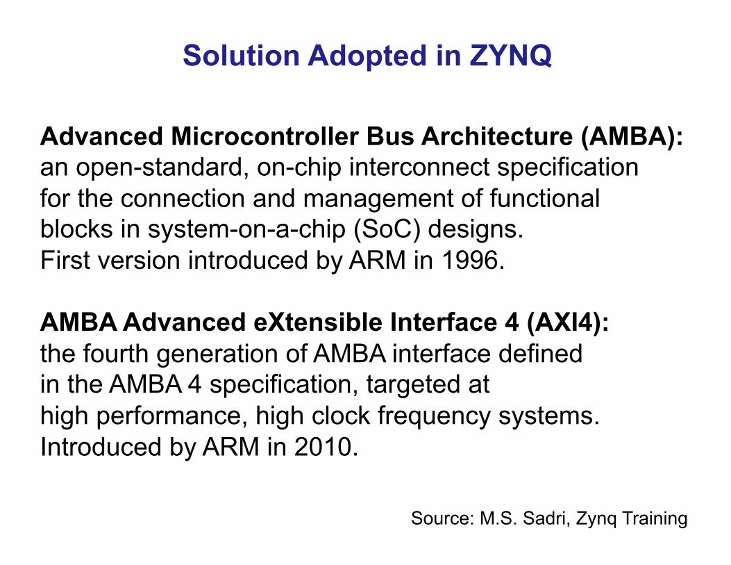
Solution Adopted in ZYNQ
Advanced Microcontroller Bus Architecture (AMBA): an open-standard, on-chip interconnect specification for the connection and management of functional blocks in system-on-a-chip (SoC) designs. First version introduced by ARM in 1996. AMBA Advanced eXtensible Interface 4 (AXI4): the fourth generation of AMBA interface defined in the AMBA 4 specification, targeted at high performance, high clock frequency systems. Introduced by ARM in 2010.
Source: M.S. Sadri, Zynq Training
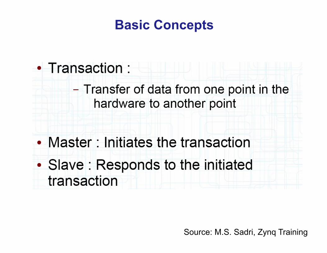
Basic Concepts

Source: M.S. Sadri, Zynq Training
Communication Between AXI Master and AXI Slave

Source: M.S. Sadri, Zynq Training
Additional Information Exchanged Between AXI Master and AXI Slave

Source: M.S. Sadri, Zynq Training
Five Channels of AXI Interface
Source: M.S. Sadri, Zynq Training
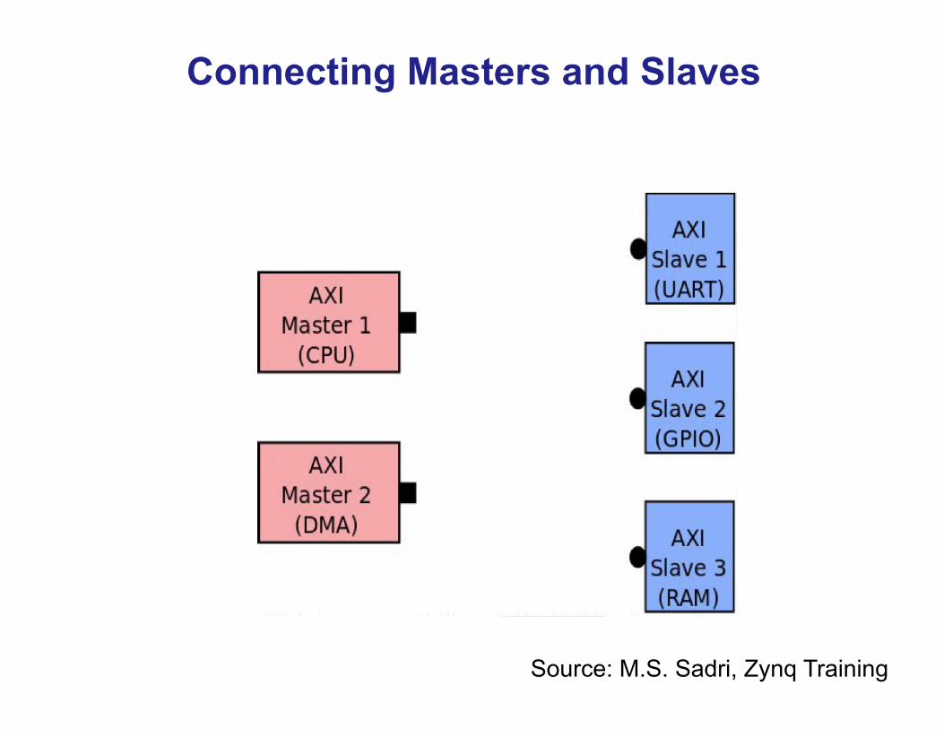
Connecting Masters and Slaves

AXI Interconnect
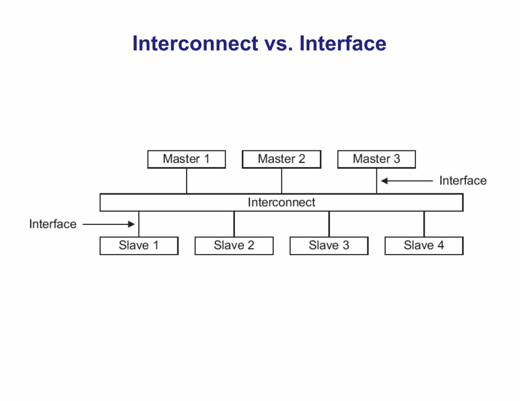
Interconnect vs. Interface

Source: M.S. Sadri, Zynq Training
Addressing of Slaves

Source: M.S. Sadri, Zynq Training
AXI Interconnect Address Decoding

Source: M.S. Sadri, Zynq Training
Clock Domain and Width Conversion
Source: M.S. Sadri, Zynq Training
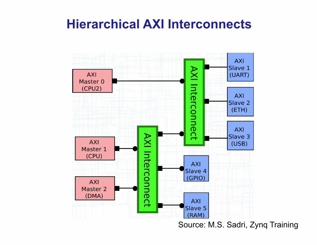
Hierarchical AXI Interconnects

Source: M.S. Sadri, Zynq Training
Simple Address Definition Rules No Overlaps

Simple Address Definition Rules Address Alignment

Source: M.S. Sadri, Zynq Training
Point-to-Point Data Flows
Source: M.S. Sadri, Zynq Training
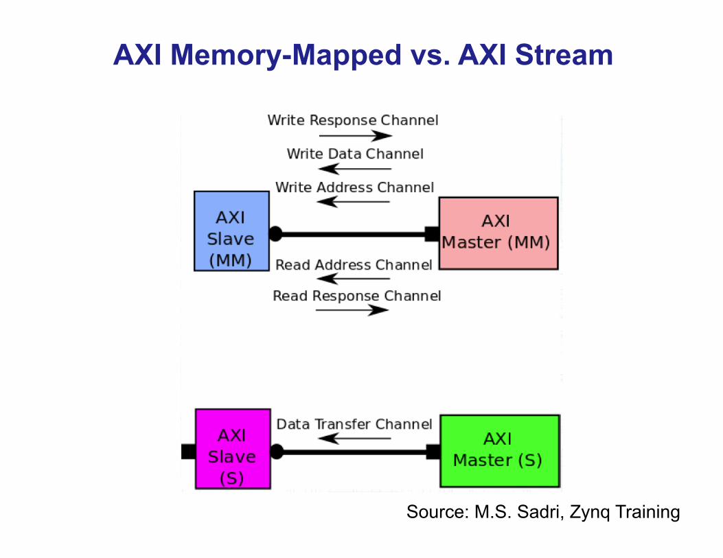
AXI Memory-Mapped vs. AXI Stream

Source: M.S. Sadri, Zynq Training
Selected AXI Stream Ports

Source: M.S. Sadri, Zynq Training
AXI Port Naming Conventions
(Shared Bus)
(Point-to-Point Bus)
(Peripheral)
(High-Performance)
Source: M.S. Sadri, Zynq Training
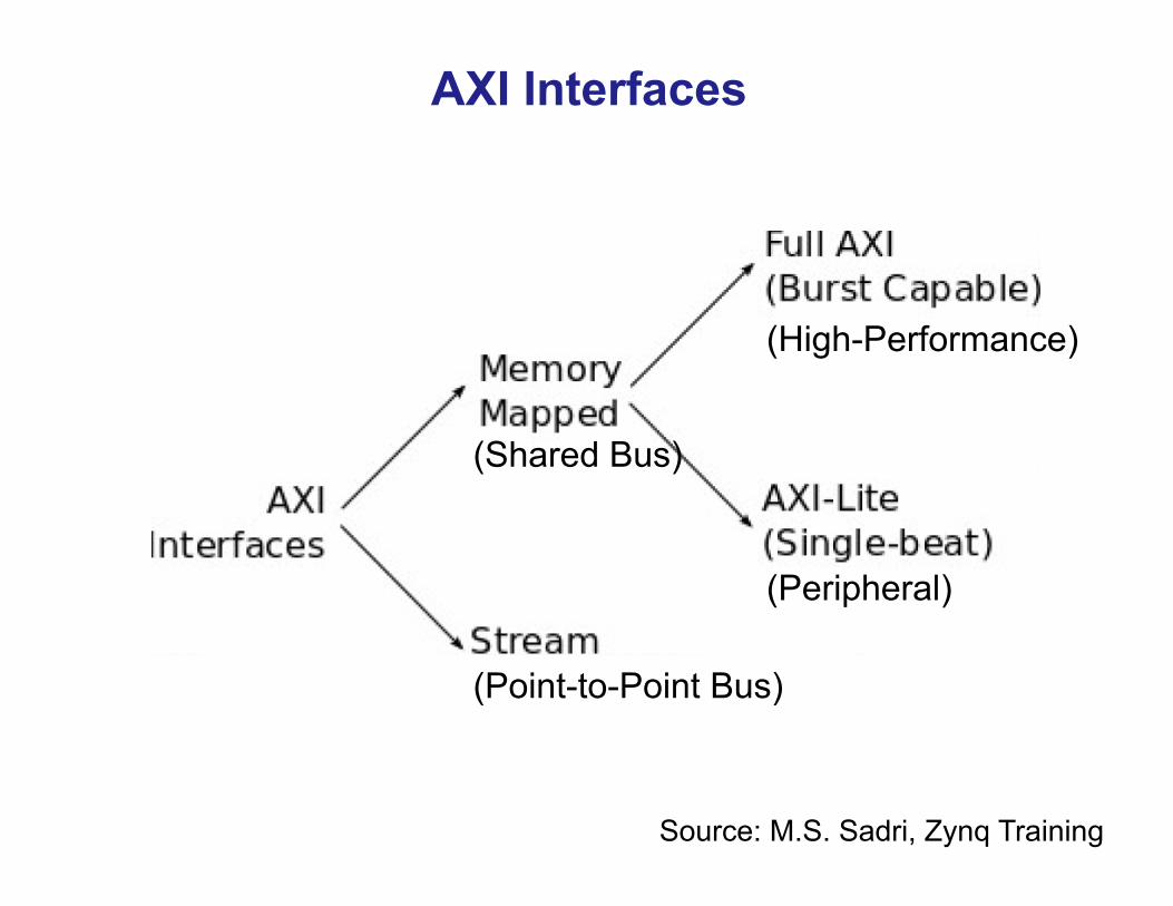
AXI Interfaces
Source: M.S. Sadri, Zynq Training
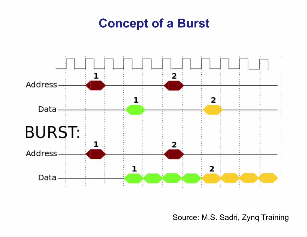
Concept of a Burst

Bus Developed by
High-Performance Shared Bus
Peripheral Shared
Bus
Point-to-Point Bus
AMBA v3 ARM AHB APB AMBA v4 ARM AXI4 AXI4-Lite AXI4-Stream
Coreconnect IBM PLB OPB Wishbone SiliCore
Corp. Crossbar Topology
Shared Topology
Point to Point Topology
Avalon Altera Avalon-MM Avalon-MM Avalon-ST AMBA: Advanced Microcontroller Bus Architecture AXI: Advanced eXtensible Interface AHB: AMBA High-speed Bus APB: AMBA Peripheral Bus PLB: Processor Local Bus OPB: On-chip Peripheral Bus MM: Memory Mapped ST: Streaming
Competing System-on-Chip Bus Standards
Source: A Practical Introduction to Hardware/Software Codesign

AXI4 Write
Source: The Zynq Book
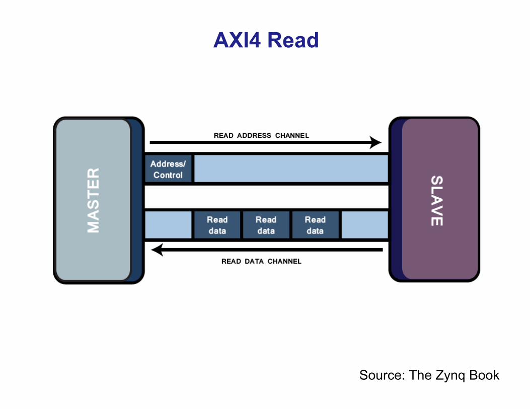
AXI4 Read
Source: The Zynq Book
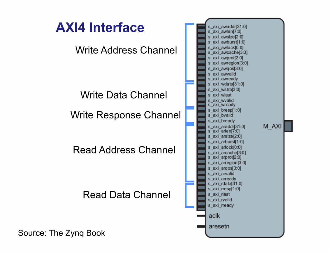
AXI4 Interface Write Address Channel
Write Data Channel
Write Response Channel
Read Address Channel
Read Data Channel
Source: The Zynq Book

Prefixes of Ports from Particular Channels
Source: The Zynq Book
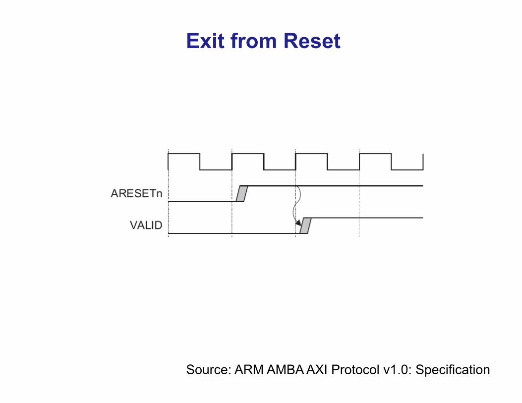
Source: ARM AMBA AXI Protocol v1.0: Specification
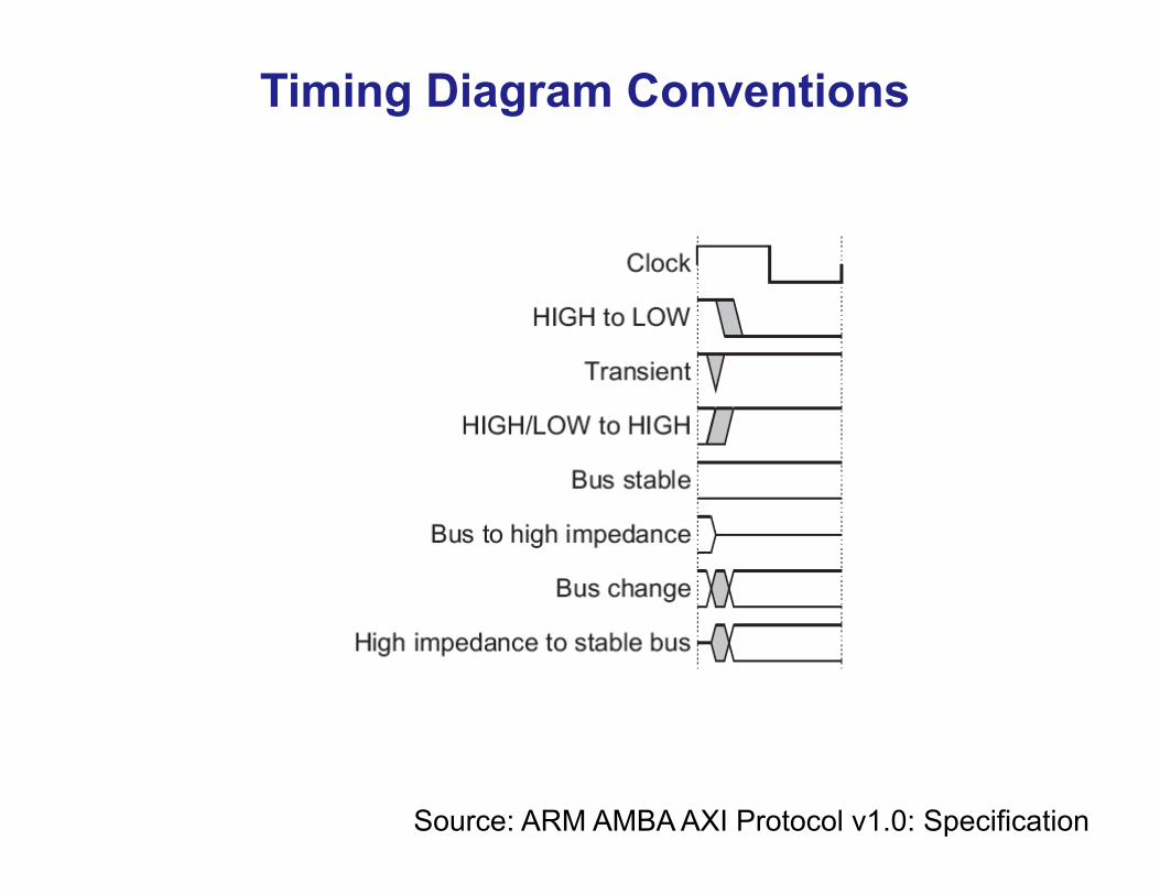
Timing Diagram Conventions

Source: ARM AMBA AXI Protocol v1.0: Specification
VALID before READY Handshake

Source: ARM AMBA AXI Protocol v1.0: Specification
READY before VALID Handshake

Source: ARM AMBA AXI Protocol v1.0: Specification
VALID with READY Handshake
Source: ARM AMBA AXI Protocol v1.0: Specification
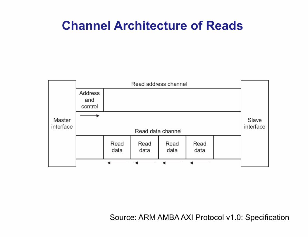
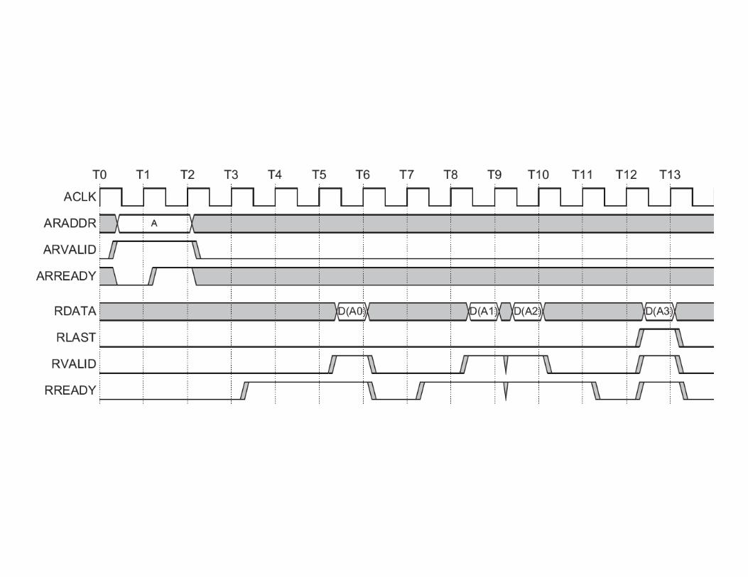
Channel Architecture of Reads

Source: ARM AMBA AXI Protocol v1.0: Specification
Read Burst

Source: ARM AMBA AXI Protocol v1.0: Specification
Overlapping Read Bursts

Read Transaction Handshake Dependencies
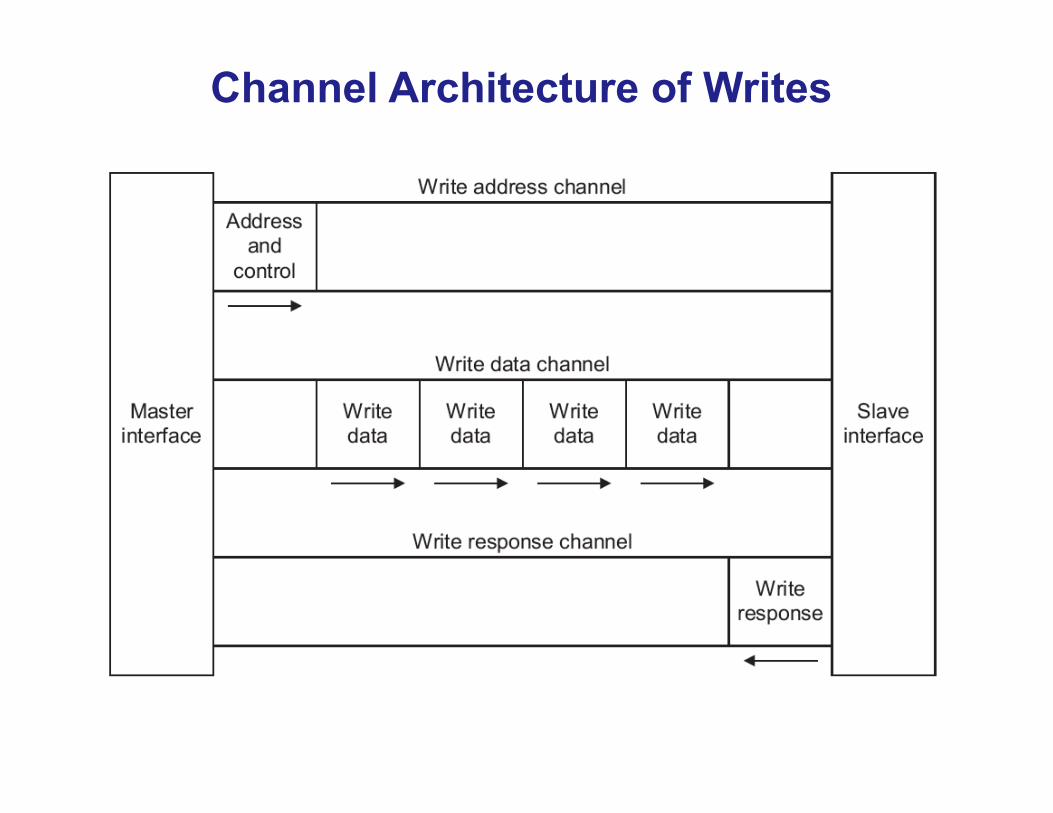
Channel Architecture of Writes
Source: ARM AMBA AXI Protocol v1.0: Specification
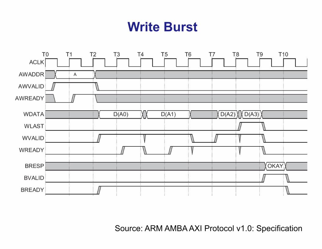
Write Burst

Source: ARM AMBA AXI Protocol v1.0: Specification
Write Transaction Handshake Dependencies

Source: ARM AMBA AXI Protocol v1.0: Specification

Source: ARM AMBA AXI Protocol v1.0: Specification
Role of Write Strobe WSTRB
WSTRB[n] corresponds to WDATA[8*n+7 downto 8*n]

Source: ARM AMBA AXI Protocol v1.0: Specification
Narrow Transfer Example with 8-bit Transfers

Source: ARM AMBA AXI Protocol v1.0: Specification
Narrow Transfer Example with 32-bit Transfers

Source: ARM AMBA AXI Protocol v1.0: Specification
Aligned and Unaligned Word Transfers on a 32-bit Bus
Source: ARM AMBA AXI Protocol v1.0: Specification
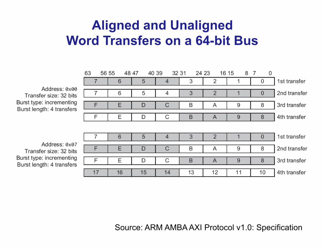
Aligned and Unaligned Word Transfers on a 64-bit Bus

Source: The Zynq Book
Example of IP Core with AXI Interface
Source: ARM AMBA AXI Protocol v1.0: Specification
Exit from Reset

Source: The Zynq Book Tutorials
Custom IP Core Used in Class Exercise

Source: The Zynq Book Tutorials
Custom IP Core Used in Class Exercise

ZYBO Board
Source: ZYBO Reference Manual
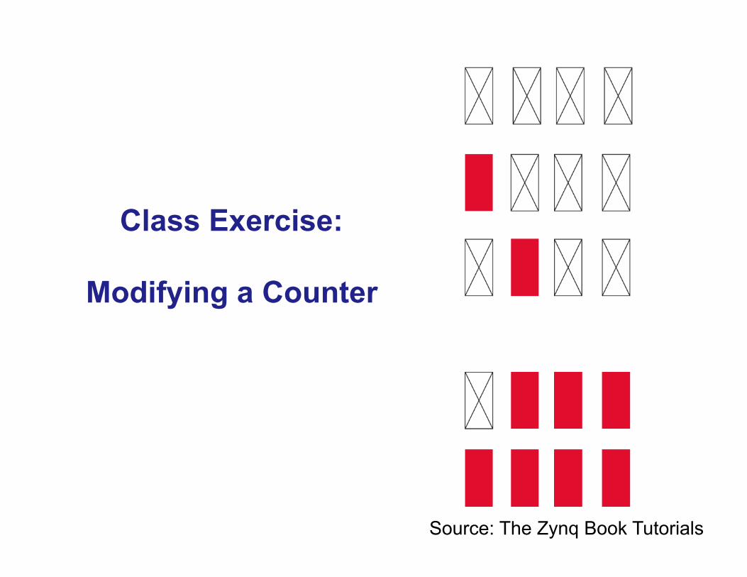
Class Exercise:
Modifying a Counter
Source: The Zynq Book Tutorials
Source: The Zynq Book Tutorials
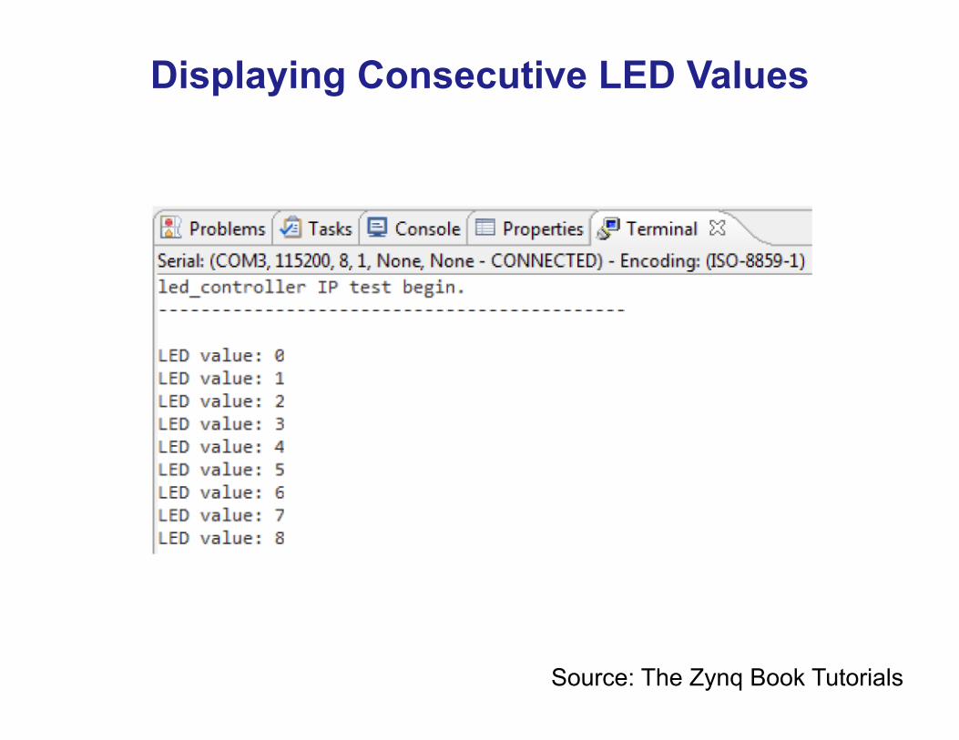
Displaying Consecutive LED Values
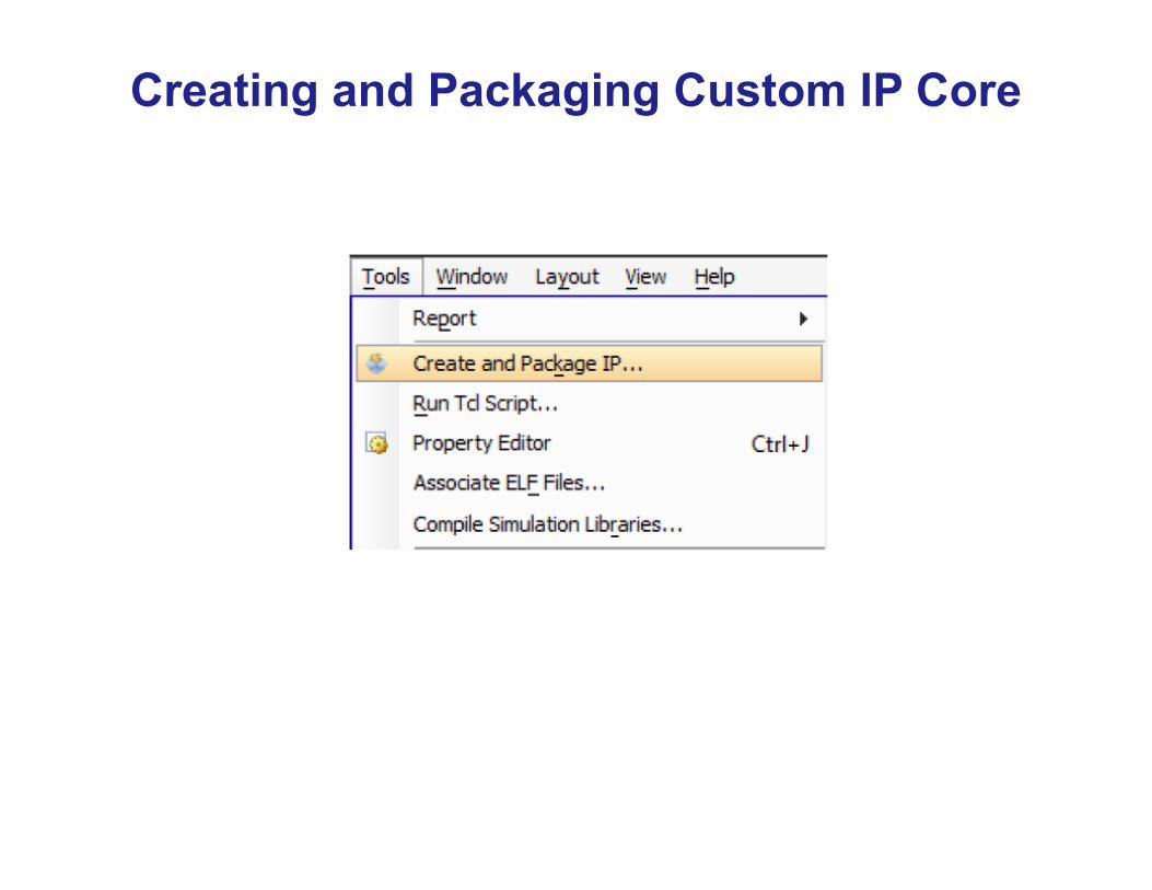
Creating and Packaging Custom IP Core
Source: The Zynq Book Tutorials
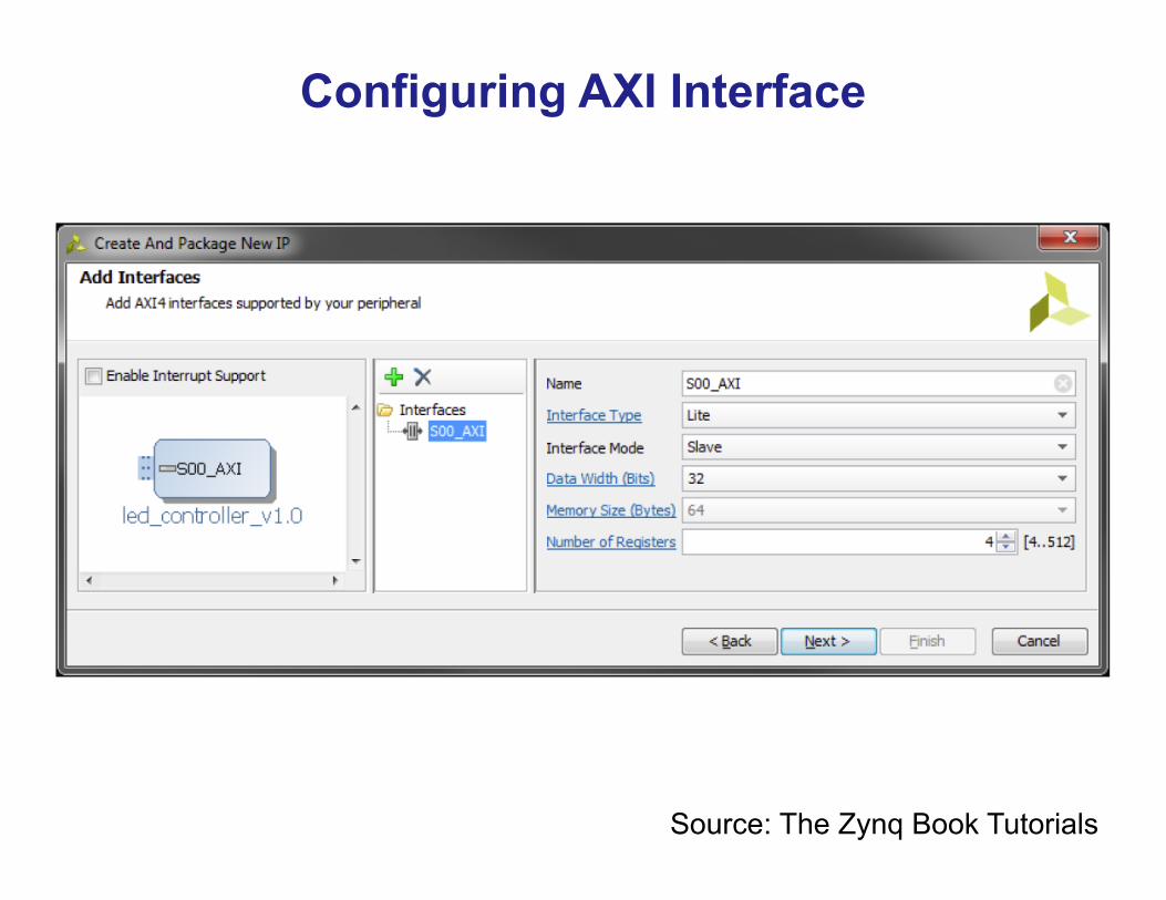
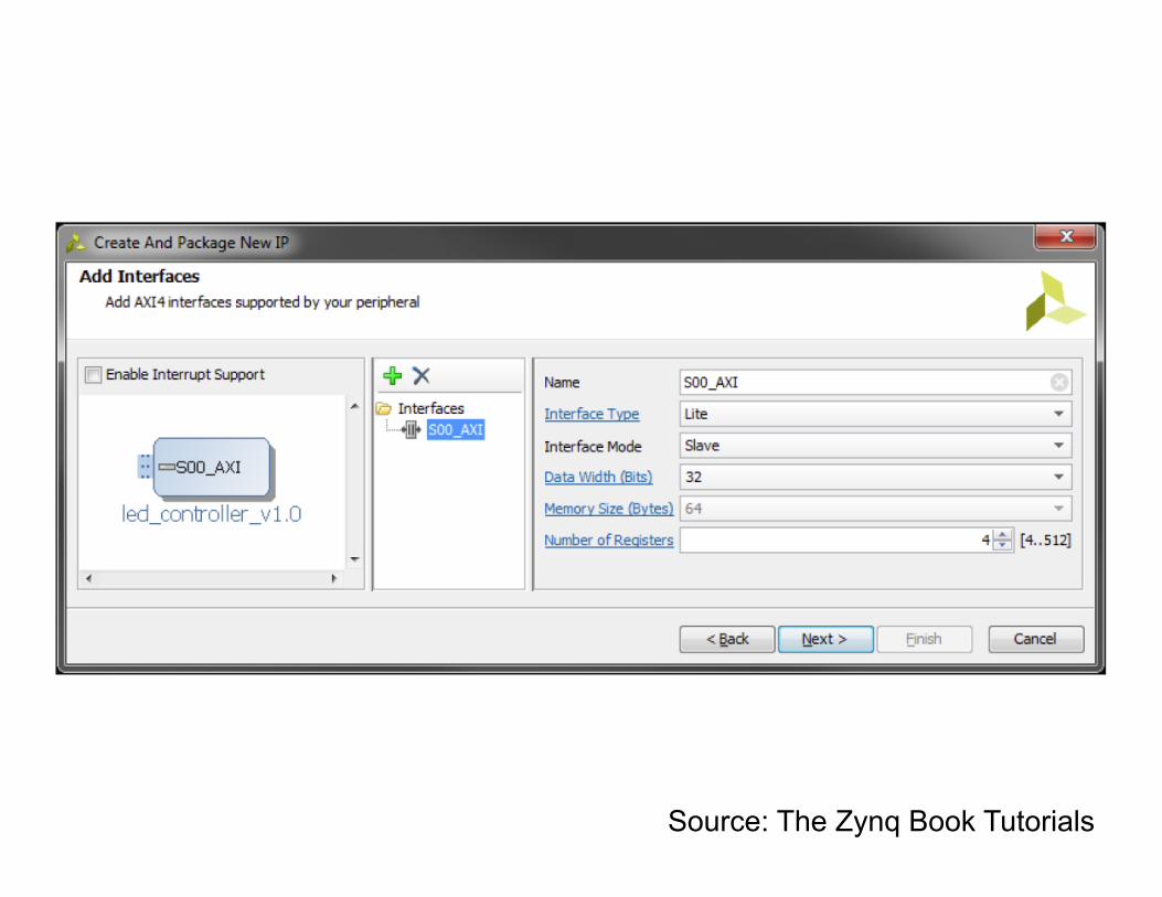
Configuring AXI Interface

Source: The Zynq Book Tutorials
Adding a Software Driver

Mapping of an Embedded SoC Hardware Architecture to Zynq
Source: Xilinx White Paper: Extensible Processing Platform

Block Design for Class Exercise

Constraint File

entity design_int_wrapper is port ( DDR_addr : inout STD_LOGIC_VECTOR ( 14 downto 0 ); DDR_ba : inout STD_LOGIC_VECTOR ( 2 downto 0 ); DDR_cas_n : inout STD_LOGIC; DDR_ck_n : inout STD_LOGIC; DDR_ck_p : inout STD_LOGIC; DDR_cke : inout STD_LOGIC; DDR_cs_n : inout STD_LOGIC; DDR_dm : inout STD_LOGIC_VECTOR ( 3 downto 0 ); DDR_dq : inout STD_LOGIC_VECTOR ( 31 downto 0 ); DDR_dqs_n : inout STD_LOGIC_VECTOR ( 3 downto 0 ); DDR_dqs_p : inout STD_LOGIC_VECTOR ( 3 downto 0 ); DDR_odt : inout STD_LOGIC; DDR_ras_n : inout STD_LOGIC; DDR_reset_n : inout STD_LOGIC; DDR_we_n : inout STD_LOGIC; FIXED_IO_ddr_vrn : inout STD_LOGIC; FIXED_IO_ddr_vrp : inout STD_LOGIC; FIXED_IO_mio : inout STD_LOGIC_VECTOR ( 53 downto 0 ); FIXED_IO_ps_clk : inout STD_LOGIC; FIXED_IO_ps_porb : inout STD_LOGIC; FIXED_IO_ps_srstb : inout STD_LOGIC; LEDs_out : out STD_LOGIC_VECTOR ( 3 downto 0 ); ); end design_int_wrapper;

design_1_i: component design_1 port map ( DDR_addr(14 downto 0) => DDR_addr(14 downto 0), DDR_ba(2 downto 0) => DDR_ba(2 downto 0), DDR_cas_n => DDR_cas_n, DDR_ck_n => DDR_ck_n, DDR_ck_p => DDR_ck_p, DDR_cke => DDR_cke, DDR_cs_n => DDR_cs_n, DDR_dm(3 downto 0) => DDR_dm(3 downto 0), DDR_dq(31 downto 0) => DDR_dq(31 downto 0), DDR_dqs_n(3 downto 0) => DDR_dqs_n(3 downto 0), DDR_dqs_p(3 downto 0) => DDR_dqs_p(3 downto 0), DDR_odt => DDR_odt, DDR_ras_n => DDR_ras_n, DDR_reset_n => DDR_reset_n, DDR_we_n => DDR_we_n, FIXED_IO_ddr_vrn => FIXED_IO_ddr_vrn, FIXED_IO_ddr_vrp => FIXED_IO_ddr_vrp, FIXED_IO_mio(53 downto 0) => FIXED_IO_mio(53 downto 0), FIXED_IO_ps_clk => FIXED_IO_ps_clk, FIXED_IO_ps_porb => FIXED_IO_ps_porb, FIXED_IO_ps_srstb => FIXED_IO_ps_srstb, LEDs_out(3 downto 0) => LEDs_out (3 downto 0) );

ZYBO General Purpose Input Output (GPIO)
Source: ZYBO Reference Manual
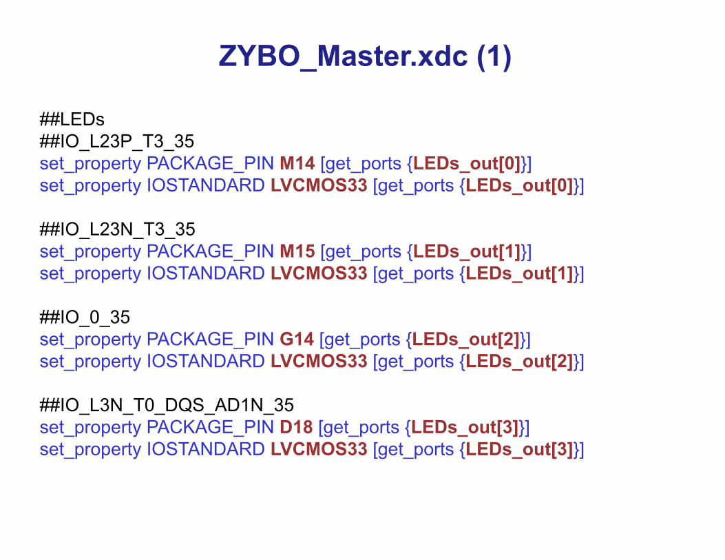
##LEDs ##IO_L23P_T3_35 set_property PACKAGE_PIN M14 [get_ports {LEDs_out[0]}] set_property IOSTANDARD LVCMOS33 [get_ports {LEDs_out[0]}] ##IO_L23N_T3_35 set_property PACKAGE_PIN M15 [get_ports {LEDs_out[1]}] set_property IOSTANDARD LVCMOS33 [get_ports {LEDs_out[1]}] ##IO_0_35 set_property PACKAGE_PIN G14 [get_ports {LEDs_out[2]}] set_property IOSTANDARD LVCMOS33 [get_ports {LEDs_out[2]}] ##IO_L3N_T0_DQS_AD1N_35 set_property PACKAGE_PIN D18 [get_ports {LEDs_out[3]}] set_property IOSTANDARD LVCMOS33 [get_ports {LEDs_out[3]}]
ZYBO_Master.xdc (1)

Main Program

/* Generated driver function for led_controller IP core */ #include "led_controller.h" #include "xparameters.h" // Define maximum LED value (2^4)-1 = 15 #define LED_LIMIT 15 // Define delay length #define DELAY 10000000 /* Define the base memory address of the led_controller IP core */ #define LED_BASE XPAR_LED_CONTROLLER_0_S00_AXI_BASEADDR
Main Program (1)

int main(void) {
/* unsigned 32-bit variables for storing current LED value */ u32 led_val = 0; int i=0;
xil_printf("led_controller IP test begin.\r\n"); xil_printf("--------------------------------------------\r\n\n");
Main Program (2)

/* Loop forever */ while(1) { while(led_val<=LED_LIMIT){ /* Print value to terminal */ xil_printf("LED value: %d\r\n", led_val); /* Write value to led_controller IP core using generated driver function */ LED_CONTROLLER_mWriteReg(LED_BASE, 0, led_val); /* increment LED value */ led_val++; /* run a simple delay to allow changes on LEDs to be visible */ for(i=0;i<DELAY;i++); }
/* Reset LED value to zero */ led_val = 0;
} return 1;
}
Main Program (3)

Device Driver led_controller.h

#include "xil_types.h" #include "xstatus.h" #define LED_CONTROLLER_S00_AXI_SLV_REG0_OFFSET 0 #define LED_CONTROLLER_S00_AXI_SLV_REG1_OFFSET 4 #define LED_CONTROLLER_S00_AXI_SLV_REG2_OFFSET 8 #define LED_CONTROLLER_S00_AXI_SLV_REG3_OFFSET 12
Device Driver (1)

/* Write a value to a LED_CONTROLLER register. A 32 bit write is performed. * If the component is implemented in a smaller width, only the least * significant data is written. * * @param BaseAddress is the base address of the LED_CONTROLLER * device. * @param RegOffset is the register offset from the base to write to. * @param Data is the data written to the register. * * @return None. * * @note C-style signature: * void LED_CONTROLLER_mWriteReg(u32 BaseAddress, * unsigned RegOffset, u32 Data) */ #define LED_CONTROLLER_mWriteReg(BaseAddress, RegOffset, Data) \ Xil_Out32((BaseAddress) + (RegOffset), (u32)(Data))
Device Driver (2)

/* Read a value from a LED_CONTROLLER register. * A 32 bit read is performed. * If the component is implemented in a smaller width, only the least * significant data is read from the register. The most significant data * will be read as 0. * * @param BaseAddress is the base address of the LED_CONTROLLER * device. * @param RegOffset is the register offset from the base to write to. * * @return Data is the data from the register. * * @note C-style signature: * u32 LED_CONTROLLER_mReadReg(u32 BaseAddress, * unsigned RegOffset) */ #define LED_CONTROLLER_mReadReg(BaseAddress, RegOffset) \ Xil_In32((BaseAddress) + (RegOffset))
Device Driver (3)
Standard IO Functions xil_io.c

/* Contains I/O functions for memory-mapped or non-memory-mapped I/O * architectures. These functions encapsulate Cortex A9 architecture-specific * I/O requirements. */
/* Performs an input operation for a 32-bit memory location by reading * from the specified address and returning the Value read from that address. * * @param Addr contains the address to perform the input operation at. * * @return The Value read from the specified input address. */ u32 Xil_In32(u32 Addr) {
return *(volatile u32 *) Addr; }
xil_io.c (1)

/* Performs an output operation for a 32-bit memory location by writing the * specified Value to the the specified address. * * @param OutAddress contains the address to perform the output * operation at. * @param Value contains the Value to be output at the specified address. * * @return None. */ void Xil_Out32(u32 OutAddress, u32 Value) {
*(volatile u32 *) OutAddress = Value; }
xil_io.c (2)

VHDL Code led_controller_v1_0_S00_AXI.vhd

entity led_controller_v1_0_S00_AXI is generic ( -- Users to add parameters here
-- User parameters ends -- Do not modify the parameters beyond this line
-- Width of S_AXI data bus C_S_AXI_DATA_WIDTH : integer := 32; -- Width of S_AXI address bus C_S_AXI_ADDR_WIDTH : integer := 4 );
Entity Declaration (1)
Source: The Zynq Book Tutorials
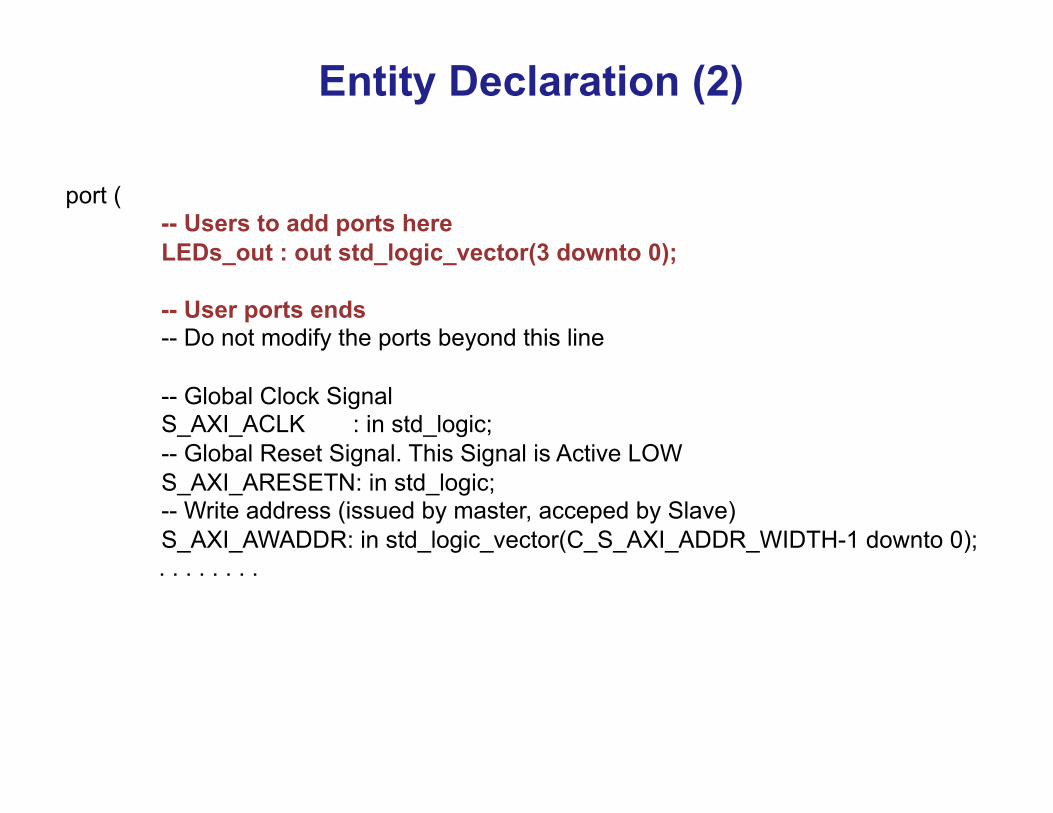
port ( -- Users to add ports here LEDs_out : out std_logic_vector(3 downto 0);
-- User ports ends -- Do not modify the ports beyond this line
-- Global Clock Signal S_AXI_ACLK : in std_logic; -- Global Reset Signal. This Signal is Active LOW S_AXI_ARESETN: in std_logic; -- Write address (issued by master, acceped by Slave) S_AXI_AWADDR: in std_logic_vector(C_S_AXI_ADDR_WIDTH-1 downto 0);
. . . . . . . .
Entity Declaration (2)

. . . . . . . . -- Read address valid. This signal indicates that the channel
-- is signaling valid read address and control information. S_AXI_ARVALID : in std_logic; -- Read address ready. This signal indicates that the slave is
-- ready to accept an address and associated control signals. S_AXI_ARREADY : out std_logic; -- Read data (issued by slave) S_AXI_RDATA : out std_logic_vector(C_S_AXI_DATA_WIDTH-1 downto 0); -- Read response. This signal indicates the status of the
-- read transfer. S_AXI_RRESP : out std_logic_vector(1 downto 0); -- Read valid. This signal indicates that the channel is
-- signaling the required read data. S_AXI_RVALID : out std_logic; -- Read ready. This signal indicates that the master can
-- accept the read data and response information. S_AXI_RREADY : in std_logic );
end led_controller_v1_0_S00_AXI;
Entity Declaration (3)

process (S_AXI_ACLK) begin if rising_edge(S_AXI_ACLK) then if S_AXI_ARESETN = '0' then axi_arready <= '0'; axi_araddr <= (others => '1'); else if (axi_arready = '0' and S_AXI_ARVALID = '1') then -- indicates that the slave has acceped the valid read address axi_arready <= '1'; -- Read Address latching axi_araddr <= S_AXI_ARADDR; else axi_arready <= '0'; end if; end if; end if; end process;
axi_arready generation
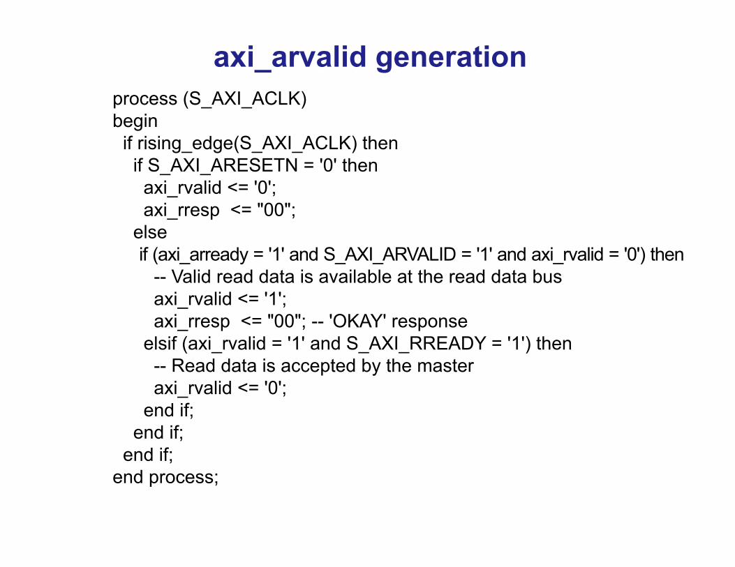
process (S_AXI_ACLK) begin if rising_edge(S_AXI_ACLK) then if S_AXI_ARESETN = '0' then axi_rvalid <= '0'; axi_rresp <= "00"; else if (axi_arready = '1' and S_AXI_ARVALID = '1' and axi_rvalid = '0') then -- Valid read data is available at the read data bus axi_rvalid <= '1'; axi_rresp <= "00"; -- 'OKAY' response elsif (axi_rvalid = '1' and S_AXI_RREADY = '1') then -- Read data is accepted by the master axi_rvalid <= '0'; end if; end if; end if; end process;
axi_arvalid generation

slv_reg_rden <= axi_arready and S_AXI_ARVALID and (not axi_rvalid) ; process (slv_reg0, slv_reg1, slv_reg2, slv_reg3, axi_araddr, S_AXI_ARESETN, slv_reg_rden) variable loc_addr :std_logic_vector(OPT_MEM_ADDR_BITS downto 0); begin -- Address decoding for reading registers loc_addr := axi_araddr(ADDR_LSB + OPT_MEM_ADDR_BITS downto ADDR_LSB); case loc_addr is
when b"00" => reg_data_out <= slv_reg0; when b"01" => reg_data_out <= slv_reg1; when b"10" => reg_data_out <= slv_reg2; when b"11" => reg_data_out <= slv_reg3; when others => reg_data_out <= (others => '0’)
end case; end process;
memory mapped read logic

process( S_AXI_ACLK ) is begin if (rising_edge (S_AXI_ACLK)) then if ( S_AXI_ARESETN = '0' ) then axi_rdata <= (others => '0'); else if (slv_reg_rden = '1') then -- When there is a valid read address (S_AXI_ARVALID) with -- acceptance of read address by the slave (axi_arready), -- output the read data -- Read address mux axi_rdata <= reg_data_out; -- register read data end if; end if; end if; end process;
memory read data

-- Add user logic here LEDs_out <= slv_reg0(3 downto 0);
-- User logic ends
end arch_imp;
User Logic