Embed Size (px)
Citation preview

1
ECE456 Lab Tutorial 3
Virtuoso Layout Editing Introduction
Contents1Introduction ...................................................................................................................................................1 2Virtuoso Layout Editing ................................................................................................................................2
2.1Setting Up the Environment .......................................................................................................................3 2.2Layer Selection Window (LSW) ................................................................................................................5 2.3Creating Shapes and Objects ......................................................................................................................6 2.4Selecting Objects for Edit...........................................................................................................................8
2.4.1Selection modes.......................................................................................................................................8 2.4.2Selecting objects ......................................................................................................................................8
2.5Editing Objects ...........................................................................................................................................8 2.5.1Moving Objects .......................................................................................................................................9 2.5.2Copying Objects ......................................................................................................................................9 2.5.3Deleting Objects ....................................................................................................................................10 2.5.4Stretching Objects..................................................................................................................................10 2.5.5Merging Objects ....................................................................................................................................11
2.6Saving the Design.....................................................................................................................................11 3 Inverter Layout : Design rule & Mask layers .............................................................................................11
3.1Design Rules.............................................................................................................................................13 3.2Mask Layers .............................................................................................................................................14
3.2.1Diffusion areas for source, drain, and substrate contacts.......................................................................14 3.2.2N-well regions .......................................................................................................................................16 3.2.3Contacts .................................................................................................................................................17 3.2.4Metal power ground and signal routing layers ......................................................................................17
4 Layout Verification ....................................................................................................................................18 4.1Design Rule Check (DRC) .......................................................................................................................18 4.2Connectivity Extraction............................................................................................................................19 4.3Layout Versus Schematic (LVS) Software...............................................................................................21
4.3.1Running LVS.........................................................................................................................................21 4.3.2Displaying the Errors.............................................................................................................................23 4.3.3Probing the Schematic and Layout ........................................................................................................24
5Layout Simulation .......................................................................................................................................25 6Hierarchal Layout Editing ...........................................................................................................................25 1 Introduction
The purpose of this lab tutorial is to guide you through the design process in creating a custom IC layout for your CMOS inverter design. The layout represents masks used in wafer fabs to fabricate a die on a silicon wafer, which then eventually are packaged to become integrated circuit chips.
Upon completion of this tutorial, you should be able to:
- Create a mask layout of the CMOS inverter that you have designed earlier - Check that your layout satisfies the design rules of a 0.25 micron process
technology - Check that your layout passes the automatic verification against that inverter
schematic created earlier

2
- Extract a netlist including parasitic resistances and capacitances from the layout - Simulate the netlist using HSPICE or Nanosim, and compare results to schematic
simulations done earlier
• The format of this tutorial is not providing step by step instruction to complete the layout design and verification but it contains enough explanations to help you to finish the basic design work.
• More information about the layout tool can be found in the online documentation
under the Layout Editor (cdsdoc command). • For the evaluation, you need to generate DRC/LVS error free layout of
inverter and InverterTest design and do the layout simulation successfully. When you do the layout simulation, use the input signal pattern that you used in the schematic simulation.
2 Virtuoso Layout Editing
• To start up the Virtuoso Layout Editor, enter grid layoutPlus in a UNIX window prompt (note the uppercase “P”). You can also use icfb instead of layoutPlus. The Main difference is that layoutPlus doesn’t provide the simulation functionality.
• When the CIW appears, select File -› New -› Cellview. Similarly, you can use
the Library Manager to create new cellviews. In the new window that appears, set Library Name to tutorial and type in inverter as the Cell Name. In the View Name field, type in layout and press the tab key. The Tool field should change to Virtuoso. Click OK to continue.
• Two windows will appear. One is called the Layer Selection Window (LSW). The LSW allows you to choose the layer on which you create objects, set which layers are selectable and set layer visibility. Note that the technology file that you entered in the first tutorial (NCSU_TechLib_tsmc03) defines the layers and colors that will be available to you in the LSW.
• The other window is the layout window (Virtuoso Layout Editing) where you
perform the place and route of the inverter layout.

3
2.1 Setting Up the Environment
Before you start doing your layout, you need to setup the grid size of the cellview so that each grid will correspond to a dimension that will make the layout process easier and allow for a more compact design. • To set up the display environment, select Options -› Display. The Display
Option window will appear. In the window, change Minor Spacing to 0.05 and Major Spacing to 0.50. Change both X Snap Spacing and Y Snap Spacing to 0.075.
• Leave other settings at their default setting. However, take note that those options will allow you to change the display of the cellview if need arises. Please refer to the online documentation if you need further information.

4
• The settings can be saved and loaded back using the Save To and Load From buttons at the bottom of the window. You can choose to save or load settings to either the cellview, library of the cellview, technology of the cellview, or a specified file. If you are saving to a file, the settings from both the Layout Editor Options and Display Options windows will be saved. Click OK when done.
• Back in the layout window, select Options -› Layout Editor. The Layout
Editor Option window will appear. Options here allow you to change the editing commands of the editor and change how the cursor behaves.
• In the Layout Editor Option window, uncheck the Gravity On box. This will
prevent the cursor from being “attracted” to other objects already drawn in the cellview. Experiment on your own. If you feel that you are comfortable with this function or find it useful in certain situations, you can turn it on. Click OK when done.
2.2 Layer Selection Window (LSW)
The Layer Selection Window (LSW) lets you to choose the layer on which you create objects (called the entry layer). It also controls which layers are selectable or visible. • To change the LSW to make layers selectable or visible, move the cursor over the
layer and click using the middle button. It will toggle layer visibility and also automatically sets invisible layers to be unselectable. The text layer color disappears to show the layer is invisible. The layer name turns gray to show the layer is not selectable.
• Every time after you have selected the layer, select Window -› Redraw to see the
effect of any LSW changes that you have made. This will allow you to make several changes in the LSW before taking time to redraw the cellview, especially in complex designs.
5
• To make the layers visible, click on the AV (All Visible) button. The colored squares showing the layer color reappear, and the shading on the layer name disappears.
• Use the left mouse button to select layers for entry in the LSW. The abbreviation
dg after each layer name means drawing (pn means pin). 2.3 Creating Shapes and Objects
Most of the layers that you will draw will be rectangles or polygons that are rectilinear in shape. The sizes of the objects depend on the design and the design rules. Creating rectangles • To create rectangles, select a layer (for example, metal1/ drw) from the LSW,
then select Create -› Rectangle or click the Rectangle icon on the left. In the new window that appears, type the net name you want the rectangle to be associated with. You can choose to leave it blank and name the net later. Shortkey for creating rectangles is ‘r’
• Note that assigning names to the nets aid in the future layout verification
processes. However, ensure that the net names on the layout matches the ones in the schematic, otherwise the LVS program (refer to section 4.3) will fail to match the nets.
• Point and click on the first corner of the rectangle, then point to the opposite
corner of the rectangle (follow the prompt in the layout window and CIW).
Creating polygons • Another way of creating objects is to create polygons. Select a layer from the
LSW, then select Create -› Polygon or click the Polygon icon on the left. In the new window that appears, type the net name you want the polygon to be associated with. You can choose to leave it blank and name the net later. Set Snap Mode to orthogonal. The snap mode controls the way segments snap to the drawing grid as you create the polygon by placing its vertices.
• Point and click on the first point of the polygon. The CIW will prompt for the
second point of the polygon. Move the cursor to click on a second point. The layout editor will create a solid line parallel to either the Y-axis or the X-axis. Continue to click on a third point that is orthogonal to the solid line. The layout editor will create two solid lines at right angles to each other between the points you entered. You will also see two dashed lines at right angles to each other attached to the two points you entered. The dashed lines show how the layout editor would finish the polygon if you click twice on this point you entered.

6
• If you made a mistake in one of the points while creating the polygon, you can
hit the Backspace key to undo them in order.
Creating Pins • In order to perform layout verification after the layout is completed (refer to
section 4.0), pins must be created to match the schematic. • To create pins, select Create -› Pin. In the window that appears, change the
Mode to shape pin. A new window named Create Shape Pin will replace the previous window.
• Enter the pin net name in the Terminal Names field. Make sure that the names
exactly match the schematic (case sensitive). If you are not sure about the names of the pin nets, open the schematic and check the net properties.
• Turn on the Display Pin Name option if you would like the pin names to be
displayed on the layout cellview. Click the Display Pin Name Option button to change the display properties of the pin names (size, font, direction etc.).
• Select the I/O Type accordingly. For power and ground pins, select
inputOutput.
• Select the layer in the LSW (use the layer that has the net abbreviation) and draw the pin in the cellview by clicking on one corner of the pin, followed by the second corner.
• If you have chosen to display the pin name in the cellview, after you have
placed the second corner of the pin, the pin name will appear next to cursor. Move the cursor to where you want the pin name placed and click.
2.4 Selecting Objects for Edit
2.4.1 Selection modes
To edit an object, first you need to select it. There are two selection modes: full and partial. Press the F4 key to toggle between selection modes and the mode is displayed in the status banner of the layout window (top). • In full selection mode (default), you select the entire object when it is clicked.
When in full mode, the status banner will display:
(F) Select: 0

7
• In partial selection mode, you can select the entire object or just edge or corner of an object. When in partial mode, the status banner will display:
(P) Select: 0
2.4.2 Selecting objects • To select an object, set the selection mode and click the object. • To deselect all objects, click in an empty part of the design.
• To select one or several objects at a time, press the Shift key while
selecting.
• To deselect one or several objects after they have been selected, press the Ctrl key and select.
2.5 Editing Objects
There are several functions that are commonly used to edit objects. They include: move, copy, delete, stretch and merge. Should you require more advanced editing methods, please refer to the Editing Objects section in the Virtuoso Layout Editor User Guide.
2.5.1 Moving Objects • To move an object, change to full selection mode and select the object(s). Notice
that when you move the cursor within the selected object, the pointer changes to four arrows. This indicates that the object(s) can be moved by clicking and dragging.
• Alternatively, you can choose to select Edit -› Move from the drop down menu or
use the Move icon on the left. The Move window appears. After you have selected the object(s), the CIW will prompt you for a reference point (start point) for the move. Click on the reference point for the move, and drag the pointer to the destination point. The object will be moved with respect to the reference point.
• Note that in the Move window, there is a Change To Layer option. This will allow
you to move and change the object from one layer to another without having to redraw the object. Check the box to enable the Change To Layer function and move the object as usual.
8
• You can rotate or flip the object (sideways or upside down) by clicking the Rotate, Sideways and Upside Down buttons in the Move window before placing the object. You can also do the same by using the right click on the mouse after you have selected the reference point for the move. Shortkey for move function is ‘m’.
2.5.2 Copying Objects • To copy an object, select Edit -› Copy or use the Copy icon after you have
selected the object(s). After the copy window appears, select the object(s) to be copied. The CIW will prompt you for a reference point (start point) for the copy. Click on the reference point for the copy, and drag the pointer to the destination point. The object will be copied with respect to the reference point. Shortkey for copy function is ‘c’.
• To copy and paste multiple copies of the object, type in the number of copies in
either the Rows or Columns fields and place the objects in the cellview as usual.
• To copy and paste an array of copied objects, enter both rows and columns. The CIW will prompt you to place the first object of the array. After you have placed the first object, continue to place the second column of the array. The distance between the first object and the second will determine the spacing and orientation between the rest of the columns. After you have placed the columns, click to place the rows of the array and complete the array. Similarly, the distance between the first and second rows will determine the spacing and orientation between the rest of the rows.
• Note that in the Copy window, there is a Change To Layer option. This will allow
you to copy and change the object from one layer to another without having to redraw the object. Check the box to enable the Change To Layer function and copy the object as usual.
• You can rotate or flip the object (sideways or upside down) by clicking the
Rotate, Sideways and Upside Down buttons in the Copy window before placing the object. You can also do the same by using the right click on the mouse after you have selected the reference point for the move
2.5.3 Deleting Objects
• To delete an object, change to full selection mode and select the object(s). Select Edit -› Delete or press the Delete key.

9
2.5.4 Stretching Objects • To stretch an object, switch to partial selection mode and select the object(s) at its
corners and edges. Notice that when you move the cursor within the selected object, the pointer changes to an arrow pointing to a line. This indicates that the object(s) can be stretched at the corners or edges by clicking and dragging.
• Alternatively, you can choose to select Edit -› Stretch from the drop down menu
or use the Stretch icon on the left. The Stretch window appears. Leave the Lock Angles option on unless you need to form nonorthogonal shapes. After you have selected the edge(s) to be stretched, the CIW will prompt you for a reference point (start point) for the stretch. Click on the reference point for the stretch, and drag the pointer to the destination point. The object will be stretched with respect to the reference point. Shortkey for stretch function is ‘s’.
2.5.5 Merging Objects • You can use the merge function to merge two objects of the same layer. To merge
objects, select the objects to be merged, then select Edit -› Merge.
2.6 Saving the Design • To save the design, select Design -› Save or click the Save icon on the left.
3 Inverter Layout : Design rule & Mask layers
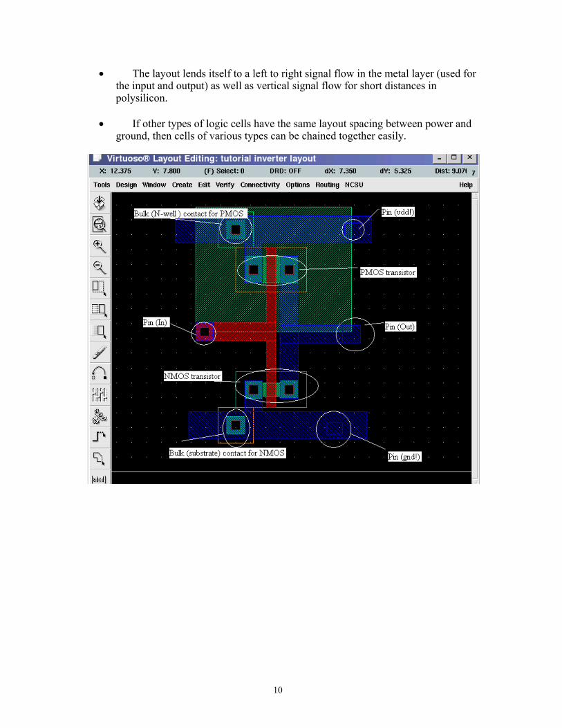
The pictures in this section present an inverter layout very similar to the one you are about to create. The only significant difference should be the transistor widths. The inverter you create should have transistor widths matching the values you determined in tutorial 1.
This layout is in the style of standard cells used for automated placement and routing of random logic. This does not, however, mean that this style of layout is bad for custom layout. It has some very useful features. In particular,
• It is designed so that multiple instances of the cell can be connected together
by abutment (i.e., placed immediately to the left and right of each other). The power, ground, input, and output connections line up and will be connected. Of course, you may wish to have the input and output not line up so that you can have the power and ground connections connect up without necessarily connecting the input and output together.
10
• The layout lends itself to a left to right signal flow in the metal layer (used for the input and output) as well as vertical signal flow for short distances in polysilicon.
• If other types of logic cells have the same layout spacing between power and
ground, then cells of various types can be chained together easily.

11
3.1 Design Rules
• Design rules are a set of rules (usually supplied by the manufacturer) that specify a minimum size or spacing requirements between layers of the same type or of different types. This provides a safety margin for various process variations, to ensure that your design will still have reasonable performance after your circuit is fabricated.
• Note that the technology file you specified in the first tutorial defines the
design rules that will be used to check your design. It also defines how the drawing layers are translated into masks for the IC. The design rule file used is divaDRC.rul.
• The following section will discuss about the more common design rules. For
other design rules, they can be found in the T-025-MM-DR-002.pdf file in the /package/eda/cells/tsmc025 directory.
12
3.2 Mask Layers
The mask layers are the various layers shown in the above diagram and are used to define the location and size of the devices and nets. Each layer can be treated as an individual layer meaning that two different layers have no electrical connection between them even though they happen to overlap. The layers are typically in different colors and shading (displayed in the Layer Selection Window – refer to section 3.2) and are defined by the display.drf file.
3.2.1 Diffusion areas for source, drain, and substrate contacts
• Rectangles on the active layer are used to define the region where doping is to be applied (except under the polysilicon gate) to form the source and drain of each transistor. For an NMOS transistor, the doping will be n+. For a PMOS transistor, this doping will be p+. It will be shown later how the type of doping is actually specified.
• Rectangles on the poly layer are used to define the strips of polysilicon used
to form the gate of each transistor and to provide short distance connections between transistors in the inverter.
• The intersection of an active and poly region defines the channel of a
transistor. Since the minimum size of active is 0.45µ and poly is 0.30µ, this means that the minimum transistor width must be 0.45µ and the minimum length must be 0.30µ.
• Note that in some cases, it may not be possible to draw an active area as a
simple rectangle. The area may have to be one width at the source and drain to accommodate the required clearance around source and drain contacts. It then may need to be notched to obtain the necessary transistor width for the intersection with poly.
• The active layer is also used to define regions that must be doped to allow a bulk (substrate or well) contact. In p- substrate, the doping must be p+ type. In an N-well (where PMOS transistors are placed), the doping must be n+ type. Note that there are square active layers in the above inverter layout example to form the bulk contacts.
• Rectangles on the n-select and p-select layers are used to control the type of dopant applied to each diffusion area. Note that these areas must extend past the diffusion area (active) by at least 0.26µ.

13
Figure 3.3. NMOS and PMOS transistors

14
Figure 3.4. N-well contact for PMOS
Figure 3.5. P-substrate contact for NMOS
3.2.2 N-well regions
• PMOS transistors must be located in substrate with N type doping. The substrate for the PMOS transistors is formed by diffusing N type dopant into regions of the normally p- type substrate. Rectangles in the nwell layer define these regions in which PMOS transistors can be placed.

15
3.2.3 Contacts
• 0.30µ x 0.30µ squares drawn on the contact (cc) layer will cause metal plugs to be placed into contact with the diffusion areas to form source, drain, and substrate or well contacts.
• 0.30µ x 0.30µ squares drawn on the contact layer will cause metal plugs to be
placed into contact with the poly areas to form poly contacts.
• Metal placed on layer metal1 will connect with these contacts.
3.2.4 Metal power ground and signal routing layers
• Rectangles on the metal1 layer define regions of aluminum to be placed in the first metal layer. In this case metal1 is used for all inputs and outputs to the inverter.
• A 0.30µ x 0.30µ square on contact provides a metal plug to connect routing
on layer metal1 to polysilicon routing below on the poly layer.
• In the 0.24µ TSMC process, there are several other metal layers available (metal2, metal3 and so on). We are not going to use it in this layout since it is not needed. However, in larger more complex layouts, both layers will be needed. Often it is a wise practice to route all signals horizontally on one layer and vertically on another layer.
• To connect the metal1 layer to the metal2 layer, a square on via12 is used.
• You can connect other metal layers together using the appropriate via layers.
For example, to connect the metal2 layer to the metal3 layer, a square on via23 is used.
4 Layout Verification
After you have completed the layout, you need to perform several verification procedures to ensure that the layout does not violate any design rules and does actually correspond with the schematic design that you have made earlier.
4.1 Design Rule Check (DRC)
DRC checks your layout against physical design rules defined in the divaDRC.rul file. It will display error information if it finds any part in the layout that violates the design rules. Note that this is only a physical design check and does not verify the actual performance or functionality of the layout design.

16
• To run DRC, select Verify -› DRC from the drop down menu. Check that the
Rules file and the Rules library fields are correct in the DRC window. Click OK to start.
• If there are any errors, it will be reported in the CIW. A blinking polygon, called
an error marker, appears in the cellview at the location of the error.
• To view the errors and get a brief description of the error, select Verify-> Markers -› Explain and click on any error marker. The marker will be highlighted in yellow to indicate that it is selected. A window named marker text will appear that contains information about the cellview that contains the error and the rule that was violated.
• To quit the Explain command, press the Esc key.
• To remove the markers, select Verify -› Markers -› Delete All. The Delete All
Markers window appears. Click OK to remove the markers.
• If any errors are reported, make changes to the layout and re-run DRC until all errors have been fixed.
• For large complex designs, it is possible to run an incremental DRC. This means
that the system will keep track of any changes you made since the last DRC and it will check only the changes made. This will make DRC run faster as it does not have to re-check every part of the design.
• To turn on incremental DRC, set the Checking Limit to incremental in the DRC
window.
• It is also possible to run a DRC on a specific area. To do this, set the Checking Limit to area in the DRC window, and click on the Sel by Cursor button. Select the area on the cellview that you want a DRC to be performed on by clicking on

17
the first point of the rectangle followed by the second point. The coordinates of the points will be entered.
4.2 Connectivity Extraction
Before performing a Layout Versus Schematic (LVS) check, you need to extract the connectivity form the layout cellview by running the Extract program. The Extract program uses rules defined in the technology file to recognize devices and establish electrical connections or nets. It will create an extracted cellview that shows the nets. • To run the Extract program, select Verify -› Extract. • In the Extractor window, select flat as the Extract Method. A flat extract method
is used because parasitic capacitance values can vary between different instances of the same cell, thus each cell must be extracted.
• Turn on Join Nets With Same Name. This will merge nets with the same names
while suppressing warning messages about different nets that have the same name.
• To select the types of parasitics that are to be extracted, click the Set Switches
button in the Extractor window. In the Set Switches window that appears, select the type of parasitics that are to be extracted (typically parasitic capacitances). Click OK when done selecting.
• Click OK or Apply in the Extractor window to create the extracted views.
• The extraction rules appear in the CIW as the extract program executes. When the
extraction is complete, a message saying that the extracted cellview is saved will be shown.
• To view the extracted cellview, select File -› Open from the CIW. It should be
under the same library and cell name. Select the extracted view name and click OK.
• The extracted cellview appears on top of the layout cellview. Notice that the
extracted cellview is similar to the layout, but the gates now have symbols at one end. Displayed next to the symbols are the gate width and length.

18
• To display the electrical connections, open the Display Options window and select Nets. Click Apply when done.
4.3 Layout Versus Schematic (LVS) Software
As its name implies, the LVS program performs a comparison of the schematic to the physical layout. It will use both the extracted view and the schematic view of the layout. If you did not create an extracted view, LVS will not work.
4.3.1 Running LVS • To run LVS, select Verify -› LVS. • If a LVS Form Contents Different window appears, click OK to continue. • In the LVS window, fill in the schematic and extracted fields either with the
Browse or Sel by Cursor button. If you choose to use the Sel by Cursor button, click on the button, then simply click in any area of the schematic or extracted cellview window.
• Note that if both the schematic and extracted cellview are opened before the LVS
window, the fields should already be filled automatically. Check to ensure that they are correct.

19
• Make sure that the specified Rules File is divaLVS.rul and the Rules Library is NCSU_TechLib_tsmc03.
• Turn off the Correspondence File option. The purpose of the correspondence file
is to allow the user to identify schematic/layout nodes that should be mapped to each other. Mainly you would do this if LVS has trouble matching the schematic and layout on its own.
• Click Run to start LVS. When the Save Cellview window appears, click OK to
save. The LVS job runs in the background and might take a couple of minutes to complete, depending on the complexity of the design. When the job is finished, a dialog box named Analysis Job Succeeded will appear. Note that this only means that the LVS program was executed successfully and does not mean that the layout matches the schematic.
• To view the LVS results, click Output in the LVS window. A text window listing
the output from the LVS run appears. Scroll down until the section that compares the layout and schematic is displayed. In that section, it will report whether the two designs match and provide a list of the numbers of instances and nets.
If LVS verifies that the layout matches the schematic, it will report: The net-lists match Otherwise, it would report: The net-lists failed to match
• If the layout fails to match the schematic, the errors on the layout must be
corrected.

20
4.3.2 Displaying the Errors • Make sure that the extracted cellview is opened before you continue. • To display the errors, click the Error Display button at the bottom of the LVS
window. • In the LVS Error Display window that appears, click the First button in the
Display field. The error message will be displayed below the Display field. In addition, the geometries in the extracted layout that do not match anything in the schematic will be highlighted in a color specified in the Error Color field.
• You can check the Auto Zoom option to zoom to the error. To clear the markers, click on the Clear Display button in the LVS Error Display window.
• If the layout matches the schematic, a netlist can be extracted from the layout to
examine the performance of the design. Otherwise, errors on the layout must be corrected, followed by a DRC run on the corrected layout, a re-extraction of the layout and a LVS run. Repeat until the final layout matches the schematic.
4.3.3 Probing the Schematic and Layout
If the layout fails to match the schematic, probing can be used to aid in finding the error. Note that this is just a tool to aid in the troubleshooting process and does not automatically locate or fix the errors. • To probe a design, click the Probe Form button in the LVS Error Display
window. • Make sure that the schematic cellview is opened before you continue (for cross
probing). • In the Probing window that appears, change Probing Method to cross probe and
click on the Add Device button.

21
• Point to a device in either the extracted or schematic cellview. The corresponding device or net that LVS has compared with will be highlighted in the other cellview.
• A single probe can be performed in a similar fashion by selecting the Probing
Method to single probe. This is useful in locating the errors when given a device or net name by LVS.
• To remove the markers, click on the Remove All button in the Probing window.
5 Layout Simulation
After you have verified that the layout matches the schematic, simulations can be performed on the extracted layout similar to the previous tutorial to determine its performance. The main difference between a schematic simulation and a layout simulation is that in a layout simulation, parasitic capacitances are extracted from the layout based on the physical dimensions and are used in the simulation. Therefore it will provide a more realistic simulation. • To perform a simulation on the extracted layout, open up the Affirma Analog
Circuit Design Environment window by selecting Tools -› Analog Environment. • The extracted layout can be simulated using HSPICE by setting up the simulator
type, type of simulation, simulation environment, input stimulus and output display, similar to simulating the schematic. Refer to the previous tutorial for more information.
• A netlist can be extracted from the extracted layout for Nanosim simulations or
HSPICE simulations, similar to simulating the schematic. Refer to the previous tutorial for more information.
6 Hierarchal Layout Editing
Circuit designs typically consist of multiple instances of the same cell. An example would be the InverterTest design that you have created in the previous tutorial. Instead of having to redraw the same layout cellview multiple times in a higher level cellview, you can place completed layout instances in the design, similar to schematic editing. Since it is ensured that each of the cells function correctly by means of LVS,

22
DRC verification and HSPICE or Nanosim simulation, placing layout instances not only saves time in drawing the cells, it means that the only errors that occur should result from connection errors. • In the Virtuoso Layout Editing window, select Create -› Instance. • In the Create Instance window that appears, enter the library and cell names in
the corresponding fields.
• Move the cursor into the cellview window. Outline of the shapes of the instance follows the cursor. Place the instance where needed.
• You can rotate or flip the instance (sideways or upside down) by clicking the
Rotate, Sideways and Upside Down buttons in the Create Instance window before placing the instance.
• Press the Esc key to quit placing more instances.
• Add layers to connect the cells together.
• Note that the layout editor does not allow you to edit the cell. However, if you
edit one of the cells at the lower level, the other cells of the same instance in the higher level will be changed.