Embed Size (px)
Citation preview

ECE145C:RF CMOS Communication
Circuits and Systems
Prof. James Buckwalter
© James Buckwalter 1

Organization
• email: [email protected]
• Lecture: Girvetz Hall 1112 8-9:15
• Faq: Piazza access code: ece145c (Gauchospace?)
• Please allow 24-48 hour turnaround
• Computing Lab: E1
• TAs– Di Li
• Office Hours: T/Th 12-1, TBD
• OH Location: ESB-2205C
© James Buckwalter 2

Scope: ECE 145C should
• refine fundamental understanding of RF circuits and systems to analyze modern wireless technology.
• present a comprehensive understanding from devices to systems.
• teach applications of RF CMOS as well as III-V
• analyze RF transmitter/receiver architectures.
© James Buckwalter 3
Modern cellular and RF technologies are a mash-up of communication theory and devices. One needs to understand device limitations to understand communication system limits and vice versa.

Topics for our class
• Propagation, Noise and Distortion Budgeting
• Basics of Modulation / Cellular Standards
• Receiver Filtering, Mixing, and Architectures
• Power Amplifiers (Linear and Nonlinear): Output power and Efficiency
• High-efficiency transmitters
• RF Architectures (Putting it all together)
© James Buckwalter 4

Lecture Topic Lecture Topic
1 (3/31) System Perspective: Link Budget
2 (4/2) System Perspective: Interference
3 (4/7) System Perspective: EVM 4 (4/9) System Perspective: Reciprocal Mixing
5 (4/14) Mixers (1) 6 (4/16) Mixers(2)
7 (4/21) Tunable Filters (I) 8 (4/23) Midterm
9 (4/28) Tunable Filters (II) 10 (4/30) RX Architectures: Mixer First
11 (5/5) RX Architectures: Direct Sampling
12 (5/7) Power Amplifiers: Classes
13 (5/12) Power Amplifiers: Classes 14 (5/14) Power Amplifiers: Spectral Regrowth
15 (5/19) OutphasingModulators…Transmitters
16 (5/21) Outphasing Modulators
17 (5/26) Doherty Transmitters 18 (5/28) Doherty Transmitters
19 (6/1) Envelope Tracking Transmitters
20 (6/3) Midterm

Reference Material
• Razavi…for now.
• These notes.
• Thomas Lee, Design of RF CMOS Integrated Circuits
• H. Darabi and A. Mirzaei, Integration of Passive RF Front End Components in SoCs
• Steve Cripps, RF Power Amplifiers for Wireless Communication

Grading
• In-class midterms 60%
• 4-5 homeworks, laboratory 25%
• Final project 15%
© James Buckwalter 7

Collaboration Policy
• Limited collaboration among students on the homework problems is encouraged. Such collaboration may include verbal discussion of problems, and the use of scratch paper or writing boards to discuss concepts and approaches to solving specific problems. It is also OK for students to verbally compare the final answers obtained for a given problem as a method of checking their work. The following academic honesty rules should be considered in force at all times:
1) Never show any draft of a homework solution to another student in the class until after the homework due date and after that person has handed in his/her own solution set.
2) Never look at any draft of another person's homework solution until after the homework due date and after you have handed in your solution set.
3) Never use another person's simulation files or supply your simulation files to another person until after the due date and after you have both handed in your solution sets.
• If any of the above academic honesty rules are violated by any student in the course, the student will receive a failing grade for the course and the incident will be reported to the dean of the student's college, in the case of an undergraduate student, or to the assistant dean of graduate studies, in the case of a graduate student, for further administrative action.

RF Wireless Systems• Communicate information reliably as quickly as possible
with as little power consumption as possible.
• Today RF systems are about coexistence Transmitter Receiver
Coding: Try to encode error correctionDAC: Digital to analog convertorMixer: Translate signal to RF carrierLO: Local OscillatorPA: Power Amplifier
PA: Power AmplifierLNA: Low Noise AmplifierADC: Analog to digital convertorCoding: Look for errors and correct data
© James Buckwalter

Shannon capacity
• Foundation of communication theory (Shannon, 1948).
• Information can be transmitted reliably at rate C.
• BW is bandwidth of the RF channel. This is typically fixed by regulations/standards.
• SNR is the signal-to-noise. This is where circuits play the most important role. Typically, we want high SNR with low power consumption.
log 1C BW SNR
© James Buckwalter 10

Bands and Channels
• We refer to RF bands and RF channels.
• Bands refers to a collection of RF frequency spectrum that is set aside for licensed or unlicensed communication.
• Channels are allocations of frequency spectrum within the band for users.
– TDD/FDD multiple access of channel
– E.g. Use one channel within band at a time.
© James Buckwalter 11

Example: LTE-A Frequency Bands (US)
© James Buckwalter 12
• Channels can be 1.4, 3, 5, 10, 15, or 20 MHz.How many channels exist in each band?

Available Bandwidth
• RF spectrum is valuable. Verizon paid $5B for 22 MHz between 746-757 and 776-787 nationwide.
• Spectral efficiency quantifies how many bits are packed into 1 Hz of bandwidth
• In reality, the modulation “spreads” over more than one hertz and degrades this ideal value without signal processing.
© James Buckwalter
SE =
C
BW= log
21+ SNR( )
13

Digital Modulation
• BPSK– mI(t) = {-1, 1}
• QPSK– mI(t) = {-1, 1}
– mQ(t) = {-1, 1}
• QAM– E.g. 16-QAM
– mI(t) = {-3, -1, 1, 3}
– mQ(t) = {-3, -1, 1, 3}
© James Buckwalter 14

Transmission of Modulated Signal
© James Buckwalter
Modulation means that large power variations can occur in the output waveform!
15
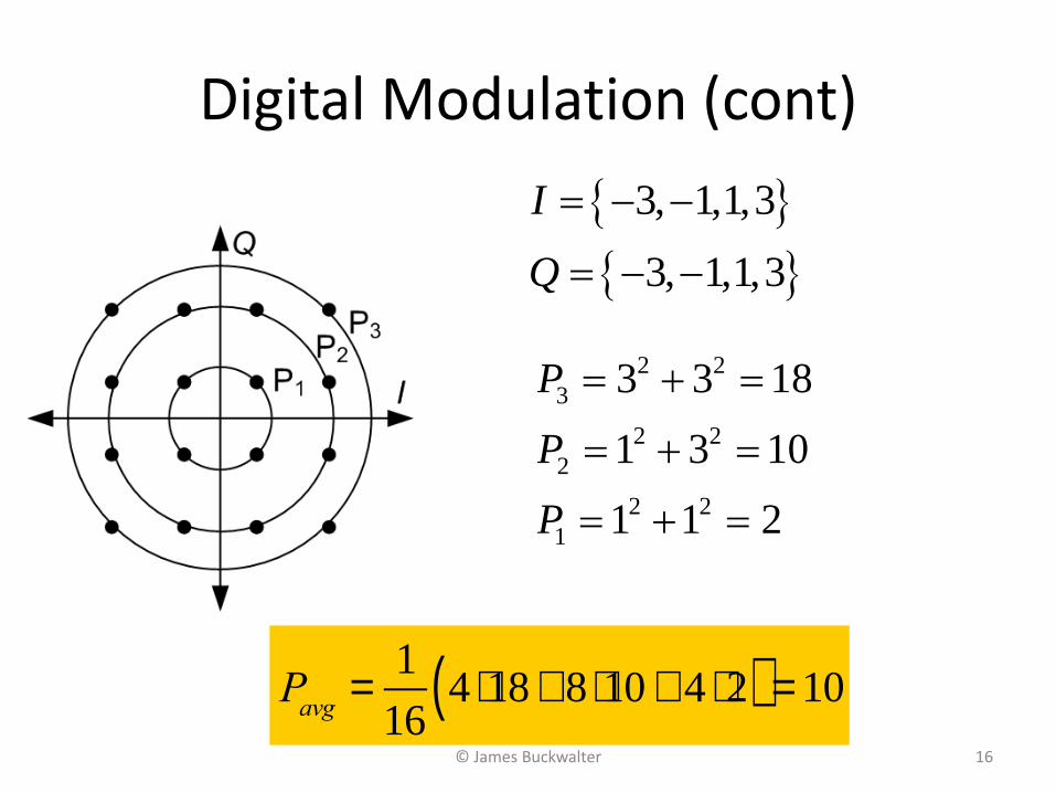
Digital Modulation (cont)
© James Buckwalter
3, 1,1,3
3, 1,1,3
I
Q
2 2
3
2 2
2
2 2
1
3 3 18
1 3 10
1 1 2
P
P
P
P
avg=
1
164 ×18 + 8 ×10 + 4 ×2( ) = 10
16

Peak-to-Average Power Ratio
• PAR or PAPR: Ratio of the peak power for the waveform relative to the average power.
• For 16-QAM
• PAPR increases for “filtered” signals.
• Big PAPR is a problem for energy-efficient circuits.
© James Buckwalter
182.5
10
peak
avg
PPAPR dB
P
17

PAPR and Dynamic Range
© James Buckwalter
• Unfiltered Modulation
• PAPR increases (dramatically for filtered signals)
Modulation Number of Symbol Power Levels
PAPR Dynamic Range % data at highest power
% data above averagepower
16-QAM 3 1.8 2.5 dB 9 9.5 dB 25% 25%
32-QAM 5 1.7 2.3 dB 17 12.3 dB 25% 50%
64-QAM 9 2.3 3.7 dB 49 16.9 dB 6.3% 50%
256-QAM 32 2.7 4.2 dB 225 23.4 dB 4.6% 45%
18

Signal-to-Noise Ratio
© James Buckwalter
d = 2E
s
oN
b
bno
o
ESNR E
N
• QPSK Illustration
• Energy-per-bit
• Noise
E
s= m
I
2 t( ) + mQ
2 t( )
19 E
b=
Es
M More on this next lecture

Signal-to-Noise, SNR
• Ebno - Energy per bit directly effects bit error rate
• 10-6 is generally acceptable for wireless
• 10-12 is generally acceptable for wireline
Pe=
1
2pe
-x2
2No
Eb
¥
ò dx = QE
b
No
æ
è
çç
ö
ø
÷÷= Q SNR( )
© James Buckwalter 20
Q x( ) =1
2pe
-t2
2
x
¥
ò dt

Spectral Efficiency and Distortion
© James Buckwalter
• Wideband signals passing through a nonlinear circuit cause spectral energy to “spill” outside of bandwidth.
• Signal processing can eliminate the energy leakage into neighboring bands but greatly increases the peak to average ratio.
21
BW

Distortion Contributions
© James Buckwalter 22
BW
In-band distortion: AM-AM (gain) compression, AM-PM compression
Out-of-band distortion
BW

Adjacent Channel Leakage Ratio
© James Buckwalter
• Compare the power of the signal in-band against the power leaking into adjacent bands.
ACLR =P fo + BW( )
P fo( )23

Tradeoffs
• Modulation– Higher-order QAM, higher capacity.
• Peak-to-average ratio (PAPR)– Higher PAPR, more distortion (in band and out of band)
• SNR– Higher SNR, higher capacity
• We want circuit solutions that offer the highest SNR, the lowest distortion, and the lowest power consumption possible.

Summary of Digital Communication
• We want to transmit as many bits per second as possible.
• I/Q are two orthogonal spaces to transmit information.
• As more bits are transmitted per second, more SNR is required to achieve the same BER.
• We guarantee circuit performance in terms of EVM. This is the ultimate measurement.
© James Buckwalter 25

PROPAGATION AND LINK BUDGETS

Propagation
• How much of the transmit power reaches the receiver?
• Power density, p(r)
• Received power
• Gt is the transmit antenna gain, Ar is the receiver area
© James Buckwalter
p r( ) =
GtP
t
4pr 2
Pt
r
P
r= G
t
Pt
4pr2A
r
27

Friis Transmission Equation
• Gr is the receive gain and λ is the wavelength of the RF signal. This gain basically depends on the size of the antenna (geometry) and type of antenna
• Remember
• The path loss is
© James Buckwalter
2
4r t t rP PG G
r
L =4pr
l
æ
èçö
ø÷
2
l =c
f
28

Path Loss
• Gt and Gr are the antenna gains. If the antennas are isotropic radiators, Gt = Gr = 1.
• Higher frequencies have inherently more loss
• A popular way to express the FriisTransmission Equation is
© James Buckwalter
Pr= P
t+ G
t+G
r+ 20log
10
l
4pr
æ
èçö
ø÷
L =4pr
l
æ
èçö
ø÷
2
29

Example Path Loss
• What is the wavelength at – 800 MHz? 2.4 GHz? 60 GHz
37.5 cm, 12.5 cm, 5mm
• What is the path loss over 1m at – 800 MHz? 2.4 GHz? 60 GHz
-30 dB, -40 dB, -68 dB
• Now, what is the path loss over 1km at– 800 MHz? 2.4 GHz? 60 GHz
-90 dB, -100 dB, -128 dB
© James Buckwalter 30

Antenna Gain
• Gain is the product of radiation efficiency and the directivity of the antenna
Gant =hant D
D = 4pUmax
Prad
æ
èç
ö
ø÷
Umax = Bo
Prad = U q ,f( )sinq dq df0
p
ò0
2p
ò
© James Buckwalter 31
Radiation Pattern in Azimuth/Elevation

Example: Lossless Antenna Gain
• Short dipole: 1.76dB
• Half-wave dipole: 2.15dB
• Horn: 10-20dB
• Parabolic: 40-50dB
© James Buckwalter 32

Antenna Model
• Antenna converts incident power to a voltage source with impedance, Zs.
• This impedance comprises– Radiation resistance Rr
– Resistive losses Rl
– Reactance Xs
REF: Antenna Theory, Balanis
© James Buckwalter 33

Example: Radiation Resistance of Half-wave Dipole (I)
• Current distribution on antenna
• Find E and H field generated by current
• Find average Poyntingvector
© James Buckwalter
2coso
zI I
l
/ 2
cos
/2
sin , ,4
ljkrjkz
l
keE j I x y z e dz
r
EH
2
2
2 2
cos cos cos1 2 2
ˆ ˆ ˆa a a2 sin8
o
av r
kl kl
IW E H
r
image: Wikipedia
34

Example: Radiation Resistance of Half-wave Dipole (II)
• Determine the radiated power
• Caveat: If maximum current does not occur at input terminals, we need to consider the input resistance rather than the radiation resistance.
©James Buckwalter
2
280rad
lR
Shorter antennas have lower radiation resistance!
2
2 0.60973rad
rad
o
PR
I
2
2
0 0
2
sin
2.4358
rad av av
o
rad
P W ds W r d d
IP
35

Example: Radiation Resistance of Half-wave Dipole (III)
• What about reactance of antenna?
→ Poynting vector does not capture transverse fields representing imaginary power
• For half-wave dipole, tangent in denominator should be very large so reactance should be small!
©James Buckwalter
log 12
120
tan2
m
l
aX
kl
Note that a corresponds to dipole wire width.
36

Here is the problem…
• We don’t have ideal voltage and current sources.
• The source resistance and load resistance create the need to “match” the source and load impedances.
• RF wavelengths are relatively short
• We need to treat RF signals as “WAVES”
• We will spend much of today understanding how we study microwave circuits.
©James Buckwalter
0.3 @ 1c
m GHzf
37

Loss and Frequency
• RF energy can interact with the atmosphere and make the situation worse
© James Buckwalter
• At low frequencies, atmospheric effects are low.
• Atmosphere is decomposed into O2 and H20 components
• Depending on conditions (raining or not) the attenuation is exacerbated at higher frequency.
38

Other Propagation Challenges
• Multipath
• Propagation consists of line of sight (LOS) and non-line of sight (NLOS) components.
© James Buckwalter 39

Multipath Fading
• Slow fading -coherence time of the channel is large relative to the delay constraint of the channel. – The amplitude and phase change imposed by the channel can
be considered roughly constant over the period of use.– Slow fading can be caused by events such as shadowing, where
a large obstruction such as a hill or large building obscures the main signal path between the transmitter and the receiver.
– The amplitude change caused by shadowing is often modeled using a log-normal distribution with a standard deviation according to the log-distance path loss model.
• Fast fading - coherence time of the channel is small relative to the delay constraint of the channel. – The amplitude and phase change imposed by the channel varies
considerably over the period of use.
© James Buckwalter 40

Multipath Fading
• Signals rarely propagate from point-to-point in a straight line
• When going through multiple reflections losses behave as 1/r4 .
• Rayleigh Fading model.
• Fading is time varying.
• Rule of thumb: Fading can add an additional 10 dB of additional loss.
© James Buckwalter
2 2exp / 4
2
r r mp r
m
41

Fading Profile Pr/Pt
d

Dealing with Multipath
• In flat fading, the coherence bandwidth of the channel is larger than the bandwidth of the signal. – All frequency components of the signal will experience the
same magnitude of fading.
– Use single carrier
• In frequency-selective fading, the coherence bandwidth of the channel is smaller than the bandwidth of the signal.– Different frequency components of the signal therefore
experience decorrelated fading.
– Use multiple carriers (OFDM)
© James Buckwalter 43

Single Carrier vs. Multi-Carrier
• Most standards use OFDM
Orthogonal Frequency Division Multiplexing
• Break bandwidth into N subcarriers
• Separate data is transmitted on separate subcarriers
• Each subcarrier is “orthogonal” © James Buckwalter 44

What does OFDM fix?
Single Carrier Multi-Carrier
Fading Selective Fading Flat Fading on subcarrier
Symbol period Short pulse (1/BW) Long Pulse (N/BW)
Equalization Large number of taps (high ISI) Short number of taps (little ISI)
Spectral efficiency Poor High
Guard bands Moderate None
© James Buckwalter 45
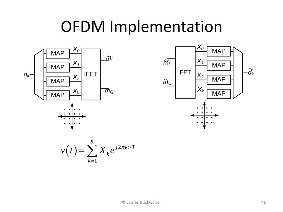
OFDM Implementation
© James Buckwalter
2 /
1
Kj kt T
k
k
v t X e
46

Peak-to-Average Power Ratio
• Multi-carrier systems impact the circuit design requirements.
• More linearity is required.
• For 16-QAM
© James Buckwalter
~ 10PAPR dB
47

Propagation Summary
• Free space path loss
• Atmospheric absorption
• Multipath fading
© James Buckwalter 48

Exercise: GPS Path Loss
• A geosynchronous satellite is located 21,000km from earth.
• The GPS band is at 1.57 GHz
• How much path loss (in dB) exists between the satellite and earth?
© James Buckwalter 49

Exercise Solution
• A geosynchronous satellite is located 21,000km from earth.
• The GPS band is at 1.57 GHz
• How much path loss exists in dB between the satellite and earth?
© James Buckwalter
L =c
f 4pr
æ
èçö
ø÷
2
=3´108 m
s4p ×1.57GHz ×21,000,000m
æ
è
ççç
ö
ø
÷÷÷
2
= -182dB
50

GPS
• If you have -182 dB of path loss, how much signal power is required to keep the receive above the minimum detectable power level?
•
© James Buckwalter 51

System Specification: Link Budget
Transmitter
Receiver
© James Buckwalter 52
How much power gets from thetransmitter to the receiver?
Or given receiver performance, how far can I reliably communicate? At what EVM? With what modulation? A link budget helps put this together

Link Budget
• We need to define a specification for our circuits.
• This can be done by figuring out how much power will travel over the RF communication link.
• The link budget is a means to put a HUGE number of parameters together and figure out the specification for the transmitter and the receiver.
© James Buckwalter 53

Link Budget Parameters
• RF Frequency: 2.4 GHz
• Data Rate: 10Mb/s
• Modulation: 16-QAM
• BER: 10-3
• Link distance: 100m
© James Buckwalter 54

Putting together a Link Budget (i)
• The following is an example.
• Start with a minimum bit error rate: 10-3
and a modulation format: 16-QAM
• Determine the minimum SNR: 12 dB
© James Buckwalter 55
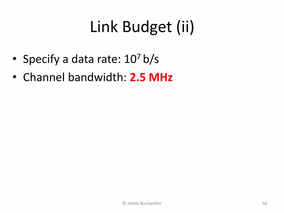
Link Budget (ii)
• Specify a data rate: 107 b/s
• Channel bandwidth: 2.5 MHz
© James Buckwalter 56

Link Budget (iii)
• Now we can assess the noise floor of our receiver.• Background noise: kT
– k is Boltzmann’s constant: 1.38x10⁻²³ J/K– T is the background temperature
• kT is -174 dBm per 1 Hz• Noise figure (NF) is a ratio that describes how
much worse than the receiver is than this fundamental background noise limit in dB. More on this later.
© James Buckwalter 57
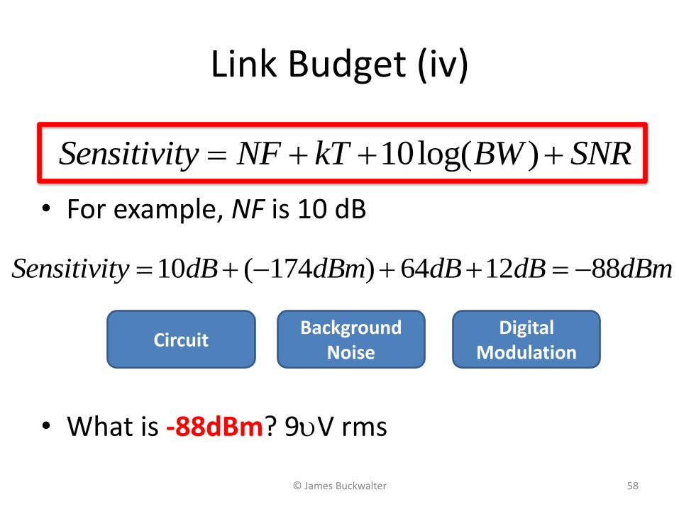
Link Budget (iv)
• For example, NF is 10 dB
• What is -88dBm? 9uV rms
© James Buckwalter
10log( )Sensitivity NF kT BW SNR
10 ( 174 ) 64 12 88Sensitivity dB dBm dB dB dBm
CircuitBackground
NoiseDigital
Modulation
58

Link Budget (v)
• We know the minimum power at the receiver.
• How much power must be transmitted?
• Start with the desired distance of transmission and the RF frequency: 1km at 2.4 GHz.
• Friis Path Loss: 100 dB
© James Buckwalter
L =4pr
l
æ
èçö
ø÷
2
L = 4p1km
0.125m
æ
èç
ö
ø÷
2
=100dB
59

Link Budget (vi)
• Other channel effects?
– Multipath fading: 10 dB
– Atmospheric absorption: 0dB
• Total propagation loss is
© James Buckwalter
Lprop
= Lpath
+ Lmultipath
Lprop
=100dB+10dB =110dB
60

Link Budget (vii)
• Now we can find the average transmit power
• The peak power can now be found.
• 24.5 dBm peak power is challenging for CMOS
• We will talk about why later.© James Buckwalter
PTX ,avg
= Sensitivity + Lprop
PTX ,avg
= -88dBm+110dB = 22dBm
PTX ,pk
= PTX ,avg
+ PAPR
PTX ,pk
= 22dBm+ 2.5dB = 24.5dBm
61

Link Budget (viii)
• Would it be better to use more bandwidth and a less dense modulation format?
• QPSK needs 8 dB to achieve the same BER
• Okay – we saved 1 dB but we have wasted twice as much bandwidth. The same performance could be sold to twice as many users.
© James Buckwalter
10log( )
10 ( 174 ) 67 8 89
Sensitivity NF kT BW SNR
Sensitivity dB dBm dB dB dBm
62

Link Budget (ix)
• What if we have more power or a different bandwidth?
• Rework the problem with the circuit specifications to determine for instance the range of transmission (next slide)
© James Buckwalter 63

Link Budget (Summary)1 element TX and RX
Transmitter
Max Pout, i.e. near OP1dB dBm 20
Backoff, i.e. ~PAPR dB 5.5
Pout on-chip dBm 14.5
Antenna
Element directivity dB 6.0
Antenna Efficiency, dB dB -3
Antenna gain dB 3
Link Budget
Effective Isotropic Radiated Power (EIRP) dBm 17.5
Bandwidth MHz 5
kTB dBm -107
Receiver NF dBm 10
Receiver noise floor dBm -97
Required AWGN SNR dB 12
Receiver sensitivity dBm -85
Receiver antenna gain dBm 3
System gain dB 105.5
Free space loss exponent, nPL 2
Free space path loss at 400 meters dB 92
© James Buckwalter
, ,TX out TX avgP P PAPR
ant ant antG D E
EIRP = Gant ,TX
+ Pout
Psens
= NF +10log10
kTB( ) + SNRmin
Gsystem
= EIRP +GANT ,RX
- Psens
Lpath
= 10 ×nPL
log10
l
4pr
æ
èçö
ø÷
The following equationsare expressed in dB
64

Equation Cheat Sheet
© James Buckwalter
10log( )Sensitivity NF kT BW SNR
1020log4
pathLr
Pr
= Pt+ G
t+ G
r+ 20log
10
l
4pr
æ
èçö
ø÷
log 1C BW SNR
N = 2MMfs = fb
, ,TX out TX avgP P PAPR
65
MDS = NF + kT +10log(BW )